EP0136183B1 - Control store arrangement for enhanced cpu pipeline performance - Google Patents
Control store arrangement for enhanced cpu pipeline performance Download PDFInfo
- Publication number
- EP0136183B1 EP0136183B1 EP84306610A EP84306610A EP0136183B1 EP 0136183 B1 EP0136183 B1 EP 0136183B1 EP 84306610 A EP84306610 A EP 84306610A EP 84306610 A EP84306610 A EP 84306610A EP 0136183 B1 EP0136183 B1 EP 0136183B1
- Authority
- EP
- European Patent Office
- Prior art keywords
- control store
- microcode
- macroinstruction
- clock period
- output lines
- Prior art date
- Legal status (The legal status is an assumption and is not a legal conclusion. Google has not performed a legal analysis and makes no representation as to the accuracy of the status listed.)
- Expired - Lifetime
Links
Images

Classifications
-
- G—PHYSICS
- G06—COMPUTING; CALCULATING OR COUNTING
- G06F—ELECTRIC DIGITAL DATA PROCESSING
- G06F9/00—Arrangements for program control, e.g. control units
- G06F9/06—Arrangements for program control, e.g. control units using stored programs, i.e. using an internal store of processing equipment to receive or retain programs
- G06F9/22—Microcontrol or microprogram arrangements
- G06F9/26—Address formation of the next micro-instruction ; Microprogram storage or retrieval arrangements
- G06F9/261—Microinstruction address formation
-
- G—PHYSICS
- G06—COMPUTING; CALCULATING OR COUNTING
- G06F—ELECTRIC DIGITAL DATA PROCESSING
- G06F9/00—Arrangements for program control, e.g. control units
- G06F9/06—Arrangements for program control, e.g. control units using stored programs, i.e. using an internal store of processing equipment to receive or retain programs
- G06F9/22—Microcontrol or microprogram arrangements
- G06F9/26—Address formation of the next micro-instruction ; Microprogram storage or retrieval arrangements
- G06F9/262—Arrangements for next microinstruction selection
- G06F9/264—Microinstruction selection based on results of processing
- G06F9/267—Microinstruction selection based on results of processing by instruction selection on output of storage
Definitions
- the present invention relates to data processors and central processing units found in data processors. More particularly, the present invention relates to control store architecture for use in implementing macroinstructions using a series of microinstructions in pipelined microinstruction execution schemes.
- CPU's Central processing units which execute macroinstructions by using a series of microinstructions in a form of pipelined manner are known in the art. Pipelining microinstruction execution generally allows a faster instruction execution throughput since while one later phase or rank of a first instruction is being executed an earlier rank of a second instruction may begin to be executed.
- Prior art pipelined control stores are usually sourced by an entry point table which decodes the macroinstruction to generate a pointer to the first microinstruction. That pointer is placed in a holding register from which it is used to access the control store. Subsequent microinstructions are addressed by either incrementing the value held in the holding register at each clock cycle or by using a field in the microcode of the first microinstruction to address the next and succeeding microinstructions.
- the process by which a macroinstruction is used to fetch a microinstruction is usually a three clock cycle event in a two rank microcode scheme.
- a first clock cycle places the entry point table value in the holding register, a second clock cycle places the rank one microcode field in a register, and a third clock cycle places the rank two microcode field in a register.
- the registered values are then used to execute the microcode functions to actually execute the instruction. Any portion of microcode that is implemented after successive clock cycles, such as rank three or higher is similarly executed.
- a control store arrangement is already known from U.S. 3 800 293 which comprises two control stores, one of which is accessed and utilized only on the first cycle of a microprogram sequence used to execute an information handling system instruction.
- a portion of the operation code of the system instruction is used to address the first- cycle control store to provide access to a microinstruction having fewer binary bits than normal microinstructions, and is effective to direct access to the remainder of the microprogram sequence contained in the other control store.
- a control store arrangement for a central processing unit having apparatus for executing macroinstructions emulated by microinstructions having a plurality of lines of microcode
- the control store arrangement includes an entry point table, addressed by said macroinstructions, for providing a pointer related to each of said microinstructions, the first control store being responsive to each of said pointers for providing on output lines connected thereto the second and subsequent lines of said microcode for each of said macroinstructions, the auxiliary control store being in the form of an entry control store connected directly to receive a pointer, included in the microinstruction, to said first line of microcode without the need for decoding by said entry point table, said entry control store containing the first line of microcode for each macroinstruction addressed by said macroinstructions, and having output lines, and selection means, responsive to microcode indicia in each of said macroinstructions which indicates that execution of the next of said macroinstructions should be started, for selectively connecting said output
- FIG. 1 a block diagram of a typical prior art control store arrangement is shown.
- a next instruction register 10 holds an instruction which is decoded by an entry point table 12 which generates an address pointing to the first line of microcode of the instruction.
- the output of entry point table 12 is placed in control store address register 14 on the clock pulse from system clock 16 which follows the availability of the valid contents of next instruction register 10.
- the first line of encoded microcode is available as a pointer to the microcode contained in control store 18.
- This line of microcode is shown diagrammatically as a bit field 20.
- Register 14 may be configured to increment the value it holds on each clock cycle to access subsequent lines of microcode for the macroinstruction or other methods may provide additional sources for addressing the control store 18.
- control store 18 may be driven by a multiplexer sourced by control store address register 14, a return stack and bit fields from the microcode to control branching as is known in the art.
- one or more registers may be interposed between control store 18 and bit field 20, and, particularly if a pipelined system is employed, at least two registers, one for rank one and one for rank two will be employed. Thus, it will take a minimum of three clock cycles before rank two information is available at the output of rank two register.
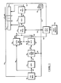
- FIG. 2 a block diagram of a control store according to the present invention is depicted.
- Next instruction register 40 contains an instruction which is decoded by entry point table 42. Specifically, the contents of next instruction register 40 address entry point table 42 via lines 46. Unlike the prior art, however, entry point table 42 does not contain a pointer to the first line of microcode for the macroinstruction being executed. Instead, it contains a pointer to the second line of microcode for the macroinstruction being executed. Entry point table 42 may be configured from read only memory, random access memory, or programmable logic arrays as is known in the art.
- the first line of microcode for each macroinstruction is contained in entry control store 48, which has access to the contents of next instruction register 40 via line 46 as does entry point table 42. Otherwise the system of Fig. 2 may operate in accordance with the control store described and claimed in our concurrently filed co-pending European application Publication No. 136182, based on United States Serial No. 537,429.
- the output of entry point table 42 is clocked into control store address register 50 via lines 52 and clock line 54 from system clock 56, on a first clock cycle. After the necessary access time has passed, this output, which is a pointer to an address in vertical control store 58, is placed into vertical control store 58 via lines 60. Subsequent microinstructions are obtained either by incrementing the value stored in control store address register 50 using clock pulses from system clock 56 or by driving line 60 from a multiplexer (not shown) whose inputs include the output of control store address register 50 as well as a return stack and bit fields from microcode to control branching in a manner known in the art. After the necessary access time, the output of vertical control store 58 is placed on control store output lines 62 via lines 64 where it is clocked into the rank one register 66 on a second clock cycle by a clock pulse from system clock 56.
- Part of the bit field in the output of rank one register 66 may be partially or fully decoded microcode forming the rank one microcode field 68 portion of microcode bit field 70.
- another portion of the output of rank one register 66 may be used as a pointer to address horizontal control store 72 via lines 74, although those skilled in the art will appreciate that this is not necessary for the invention to function properly.
- the output of horizontal control store 72 is available to the input of rank two register 76 via lines 77.
- the output of horizontal control store 72 is placed into rank two register 76, and is available as rank two portion 78 of microcode bit field 70.
- this third clock cycle it is the second line of microcode being executed in rank two rather than the rank two information of the first line.
- a selected bit field 80 which may be one or more bits within the rank one bit field 68 in microcode field 70 is used in conjunction with entry control store 48 to execute the first line of microcode.
- the state of this field, decoded if necessary, is placed via line 82 into entry control store enable register 84 on each clock cycle from system clock 56.
- the output of entry control store enable register 84, via line 86, is presented to the enable inputs of entry control store 48 and vertical control store 58.
- Input EN 88 of entry control store 48 is logic low active and input EN 90 of vertical control store 58 is logic high active. Since both entry control store 48 and vertical control store 58 share control store output bus 62, their EN and EN inputs assure that only one has control of the bus at any given time.
- Another selected bit field 91 via line 93 acts to inhibit the clock pulse to next instruction register 40 except during the cycle the next instruction is to be loaded. This will happen one or more clock pulses before bit field 80 enables the entry control store 48. As the timing is instruction dependent, those skilled in the art will recognize when this has to take place with respect to a given instruction sequence.
- entry control store register 84 may be inhibited in order to continue execution of microinstructions out of vertical control store 58.
- the result of a test which is used to make the microbranching decision shown diagrammatically at 92, may be used to inhibit entry control store register 84 from selecting entry control store 48.
- macroinstructions having two lines of microcode may be executed without the need to insert a NOP (no operation) space filler to in essence halt the system while the first pointer to the first line of microcode propagates through control store address register 50 in order to perform the instruction decode in vertical control store 58.
- NOP no operation
- the branch target In performing a macrobranch, the branch target is loaded into the next instruction register 40, but execution of the target macroinstruction cannot begin until the rank one portion of its first line of microcode is available on the control store output lines 62. With the present invention, this requires only a single clock for the access of the entry control store 48. Otherwise, two clocks would be required in order to first access an entry point table 42 followed the next cycle by the access of the vertical control store 58.
Landscapes
- Engineering & Computer Science (AREA)
- Software Systems (AREA)
- Theoretical Computer Science (AREA)
- Physics & Mathematics (AREA)
- General Engineering & Computer Science (AREA)
- General Physics & Mathematics (AREA)
- Advance Control (AREA)
- Executing Machine-Instructions (AREA)
- Control Of Non-Positive-Displacement Pumps (AREA)
- Combined Controls Of Internal Combustion Engines (AREA)
- Memory System Of A Hierarchy Structure (AREA)
- Electrical Discharge Machining, Electrochemical Machining, And Combined Machining (AREA)
- Hardware Redundancy (AREA)
- Communication Control (AREA)
Abstract
Description
- The present invention relates to data processors and central processing units found in data processors. More particularly, the present invention relates to control store architecture for use in implementing macroinstructions using a series of microinstructions in pipelined microinstruction execution schemes.
- Central processing units (CPU's) which execute macroinstructions by using a series of microinstructions in a form of pipelined manner are known in the art. Pipelining microinstruction execution generally allows a faster instruction execution throughput since while one later phase or rank of a first instruction is being executed an earlier rank of a second instruction may begin to be executed.
- Prior art pipelined control stores are usually sourced by an entry point table which decodes the macroinstruction to generate a pointer to the first microinstruction. That pointer is placed in a holding register from which it is used to access the control store. Subsequent microinstructions are addressed by either incrementing the value held in the holding register at each clock cycle or by using a field in the microcode of the first microinstruction to address the next and succeeding microinstructions.
- The process by which a macroinstruction is used to fetch a microinstruction is usually a three clock cycle event in a two rank microcode scheme. A first clock cycle places the entry point table value in the holding register, a second clock cycle places the rank one microcode field in a register, and a third clock cycle places the rank two microcode field in a register. The registered values are then used to execute the microcode functions to actually execute the instruction. Any portion of microcode that is implemented after successive clock cycles, such as rank three or higher is similarly executed.
- Because of the nature of pipelined systems, multiple clock cycles for the execution of a single line of microcode are required. This fact of instruction execution is one of the factors which determines instruction throughput in data processing systems. Since throughput and speed are important considerations in data processing systems any improvement in the instruction execution portion of a data processing system will result in increased system performance.
- A control store arrangement is already known from U.S. 3 800 293 which comprises two control stores, one of which is accessed and utilized only on the first cycle of a microprogram sequence used to execute an information handling system instruction. A portion of the operation code of the system instruction is used to address the first- cycle control store to provide access to a microinstruction having fewer binary bits than normal microinstructions, and is effective to direct access to the remainder of the microprogram sequence contained in the other control store.
- It is an object of the present invention to modify the known arrangement so as to provide a control store which enables the execution of the first line of microcode of a macroinstruction in a pipelined CPU in fewer clock cycles than is possible in currently known systems.
- In accordance with the present invention, there is provided a control store arrangement for a central processing unit having apparatus for executing macroinstructions emulated by microinstructions having a plurality of lines of microcode, wherein the control store arrangement includes an entry point table, addressed by said macroinstructions, for providing a pointer related to each of said microinstructions, the first control store being responsive to each of said pointers for providing on output lines connected thereto the second and subsequent lines of said microcode for each of said macroinstructions, the auxiliary control store being in the form of an entry control store connected directly to receive a pointer, included in the microinstruction, to said first line of microcode without the need for decoding by said entry point table, said entry control store containing the first line of microcode for each macroinstruction addressed by said macroinstructions, and having output lines, and selection means, responsive to microcode indicia in each of said macroinstructions which indicates that execution of the next of said macroinstructions should be started, for selectively connecting said output lines of said first control store or said output lines of said entry control store to said bus, and further including inhibit means in said selection means, responsive to a test result signal, for inhibiting the connection of said output lines of said entry control store to said bus.
- The invention is described further hereinafter, by way of example only, with reference to the accompanying drawings, in which:
- Fig. 1 is a block diagram of a typical prior art control store arrangement; and
- Fig. 2 is a block diagram of a control store configured according to the present invention.
- Referring first to Fig. 1, a block diagram of a typical prior art control store arrangement is shown. A next instruction register 10 holds an instruction which is decoded by an entry point table 12 which generates an address pointing to the first line of microcode of the instruction. The output of entry point table 12 is placed in control
store address register 14 on the clock pulse from system clock 16 which follows the availability of the valid contents of next instruction register 10. After the clock pulse, the first line of encoded microcode is available as a pointer to the microcode contained incontrol store 18. This line of microcode is shown diagrammatically as abit field 20.Register 14 may be configured to increment the value it holds on each clock cycle to access subsequent lines of microcode for the macroinstruction or other methods may provide additional sources for addressing thecontrol store 18. For instance,control store 18 may be driven by a multiplexer sourced by controlstore address register 14, a return stack and bit fields from the microcode to control branching as is known in the art. - As is also known in the art, one or more registers (not shown) may be interposed between
control store 18 andbit field 20, and, particularly if a pipelined system is employed, at least two registers, one for rank one and one for rank two will be employed. Thus, it will take a minimum of three clock cycles before rank two information is available at the output of rank two register. - Referring now to Fig. 2, a block diagram of a control store according to the present invention is depicted.
-
Next instruction register 40 contains an instruction which is decoded by entry point table 42. Specifically, the contents ofnext instruction register 40 address entry point table 42 vialines 46. Unlike the prior art, however, entry point table 42 does not contain a pointer to the first line of microcode for the macroinstruction being executed. Instead, it contains a pointer to the second line of microcode for the macroinstruction being executed. Entry point table 42 may be configured from read only memory, random access memory, or programmable logic arrays as is known in the art. - The first line of microcode for each macroinstruction is contained in
entry control store 48, which has access to the contents ofnext instruction register 40 vialine 46 as does entry point table 42. Otherwise the system of Fig. 2 may operate in accordance with the control store described and claimed in our concurrently filed co-pending European application Publication No. 136182, based on United States Serial No. 537,429. - The execution of the second and any following lines of microcode will be disclosed, followed by a disclosure of the manner in which the first line of microcode is placed into the pipeline at a point in time earlier than is possible using prior art configurations.
- The output of entry point table 42 is clocked into control store address register 50 via
lines 52 andclock line 54 fromsystem clock 56, on a first clock cycle. After the necessary access time has passed, this output, which is a pointer to an address invertical control store 58, is placed intovertical control store 58 via lines 60. Subsequent microinstructions are obtained either by incrementing the value stored in controlstore address register 50 using clock pulses fromsystem clock 56 or by driving line 60 from a multiplexer (not shown) whose inputs include the output of controlstore address register 50 as well as a return stack and bit fields from microcode to control branching in a manner known in the art. After the necessary access time, the output ofvertical control store 58 is placed on controlstore output lines 62 vialines 64 where it is clocked into the rank oneregister 66 on a second clock cycle by a clock pulse fromsystem clock 56. - Part of the bit field in the output of rank one
register 66 may be partially or fully decoded microcode forming the rank onemicrocode field 68 portion ofmicrocode bit field 70. In a preferred embodiment, another portion of the output of rank oneregister 66 may be used as a pointer to addresshorizontal control store 72 vialines 74, although those skilled in the art will appreciate that this is not necessary for the invention to function properly. After the necessary access time, the output ofhorizontal control store 72 is available to the input of rank two register 76 vialines 77. On a third clock cycle fromsystem clock 56 vialine 54 the output ofhorizontal control store 72 is placed into rank two register 76, and is available as rank twoportion 78 ofmicrocode bit field 70. However, those skilled in the art will realize that on this third clock cycle it is the second line of microcode being executed in rank two rather than the rank two information of the first line. - A
selected bit field 80, which may be one or more bits within the rank onebit field 68 inmicrocode field 70 is used in conjunction withentry control store 48 to execute the first line of microcode. The state of this field, decoded if necessary, is placed vialine 82 into entry control store enable register 84 on each clock cycle fromsystem clock 56. The output of entry control store enable register 84, vialine 86, is presented to the enable inputs ofentry control store 48 andvertical control store 58. Input EN 88 ofentry control store 48 is logic low active and input EN 90 ofvertical control store 58 is logic high active. Since bothentry control store 48 andvertical control store 58 share controlstore output bus 62, their EN and EN inputs assure that only one has control of the bus at any given time. This may be accomplished, as is known in the art, by multiplexing them both on tobus 62, or by selectively disabling the output drivers of one or the other ofvertical control store 58 andentry control store 48. Most of the time,vertical control store 58 has control of the bus, which meansfield 80 will cause ECS register 84 to contain a logic high level (a "one"). However, when the next macroinstruction has been loaded intonext instruction register 40, typically during execution of the next to last microinstruction of the macroinstruction currently being executed,entry control store 48 takes control of controlstore output bus 62 and places the first line of microcode for that next macroinstruction on controlstore output bus 62. This process occurs a clock cycle earlier then it could be placed there if it entered the pipeline at the output of entry point table 42. In such case the instruction would need to be decoded in entry point table 41 and the pointer would have to wait for the next clock pulse to be placed in controlstore address register 50. The pointer would then access microcode fromvertical control store 58 which would then be placed on controlstore output lines 62, before it could be clocked into in rank oneregister 66. - Another
selected bit field 91 vialine 93 acts to inhibit the clock pulse tonext instruction register 40 except during the cycle the next instruction is to be loaded. This will happen one or more clock pulses beforebit field 80 enables theentry control store 48. As the timing is instruction dependent, those skilled in the art will recognize when this has to take place with respect to a given instruction sequence. - To facilitate microbranching, the action of entry control store register 84 may be inhibited in order to continue execution of microinstructions out of
vertical control store 58. In a preferred embodiment, the result of a test which is used to make the microbranching decision, shown diagrammatically at 92, may be used to inhibit entry control store register 84 from selectingentry control store 48. - This feature is most significant for execution of macroinstructions which contain fewer than three lines of microinstructions. If the number of microinstructions is three or greater, system microcoders could improve pipelining by placing the directive to fetch the next macroinstruction and place it in next instruction register one microinstruction line sooner. This, of course, cannot be done with instructions having fewer than three lines.
- With the present invention, macroinstructions having two lines of microcode may be executed without the need to insert a NOP (no operation) space filler to in essence halt the system while the first pointer to the first line of microcode propagates through control
store address register 50 in order to perform the instruction decode invertical control store 58. - Those skilled in the art will recognize that the same mechanism which reduces the minimum macroinstruction execution time, also reduces the time required to execute macroinstruction branches.
- In performing a macrobranch, the branch target is loaded into the
next instruction register 40, but execution of the target macroinstruction cannot begin until the rank one portion of its first line of microcode is available on the control store output lines 62. With the present invention, this requires only a single clock for the access of theentry control store 48. Otherwise, two clocks would be required in order to first access an entry point table 42 followed the next cycle by the access of thevertical control store 58.
Claims (2)
Priority Applications (1)
| Application Number | Priority Date | Filing Date | Title |
|---|---|---|---|
| AT84306610T ATE54212T1 (en) | 1983-09-29 | 1984-09-28 | CONTROL MEMORY ARRANGEMENT FOR IMPLEMENTING A CPU PIPELINE. |
Applications Claiming Priority (2)
| Application Number | Priority Date | Filing Date | Title |
|---|---|---|---|
| US06/537,038 US4574344A (en) | 1983-09-29 | 1983-09-29 | Entry control store for enhanced CPU pipeline performance |
| US537038 | 1990-06-12 |
Publications (3)
| Publication Number | Publication Date |
|---|---|
| EP0136183A2 EP0136183A2 (en) | 1985-04-03 |
| EP0136183A3 EP0136183A3 (en) | 1986-02-26 |
| EP0136183B1 true EP0136183B1 (en) | 1990-06-27 |
Family
ID=24140919
Family Applications (1)
| Application Number | Title | Priority Date | Filing Date |
|---|---|---|---|
| EP84306610A Expired - Lifetime EP0136183B1 (en) | 1983-09-29 | 1984-09-28 | Control store arrangement for enhanced cpu pipeline performance |
Country Status (8)
| Country | Link |
|---|---|
| US (1) | US4574344A (en) |
| EP (1) | EP0136183B1 (en) |
| JP (1) | JPH071479B2 (en) |
| AT (1) | ATE54212T1 (en) |
| AU (1) | AU571010B2 (en) |
| CA (1) | CA1227578A (en) |
| DE (1) | DE3482607D1 (en) |
| NO (1) | NO843893L (en) |
Families Citing this family (22)
| Publication number | Priority date | Publication date | Assignee | Title |
|---|---|---|---|---|
| US4800486A (en) * | 1983-09-29 | 1989-01-24 | Tandem Computers Incorporated | Multiple data patch CPU architecture |
| US4812972A (en) * | 1984-06-20 | 1989-03-14 | Convex Computer Corporation | Microcode computer having dispatch and main control stores for storing the first and the remaining microinstructions of machine instructions |
| US4794527A (en) * | 1986-01-29 | 1988-12-27 | Digital Equipment Corporation | Microprogrammed data processing system using latch circuits to access different control stores with the same instruction at different times |
| US4890218A (en) * | 1986-07-02 | 1989-12-26 | Raytheon Company | Variable length instruction decoding apparatus having cross coupled first and second microengines |
| US5235686A (en) * | 1987-02-24 | 1993-08-10 | Texas Instruments Incorporated | Computer system having mixed macrocode and microcode |
| US5101341A (en) * | 1988-08-25 | 1992-03-31 | Edgcore Technology, Inc. | Pipelined system for reducing instruction access time by accumulating predecoded instruction bits a FIFO |
| JPH0769791B2 (en) * | 1988-12-21 | 1995-07-31 | 三菱電機株式会社 | Microprocessor |
| US5333287A (en) * | 1988-12-21 | 1994-07-26 | International Business Machines Corporation | System for executing microinstruction routines by using hardware to calculate initialization parameters required therefore based upon processor status and control parameters |
| EP0388735A3 (en) * | 1989-03-10 | 1993-01-13 | Nec Corporation | Microprogram controller having fixed-instruction generator and microprogram memory |
| US5293592A (en) * | 1989-04-07 | 1994-03-08 | Intel Corporatino | Decoder for pipelined system having portion indicating type of address generation and other portion controlling address generation within pipeline |
| GB2230116B (en) * | 1989-04-07 | 1993-02-17 | Intel Corp | An improvement for pipelined decoding of instructions in a pipelined processor |
| CA2030404A1 (en) * | 1989-11-27 | 1991-05-28 | Robert W. Horst | Microinstruction sequencer |
| US5377335A (en) * | 1991-08-30 | 1994-12-27 | Unisys Corporation | Multiple alternate path pipelined microsequencer and method for controlling a computer |
| JP3497516B2 (en) * | 1992-02-20 | 2004-02-16 | 株式会社ルネサステクノロジ | Data processor |
| US5471626A (en) * | 1992-05-06 | 1995-11-28 | International Business Machines Corporation | Variable stage entry/exit instruction pipeline |
| EP0661877B1 (en) * | 1993-12-28 | 2000-02-23 | Sony Corporation | Information signal transmission devices |
| US5790825A (en) * | 1995-11-08 | 1998-08-04 | Apple Computer, Inc. | Method for emulating guest instructions on a host computer through dynamic recompilation of host instructions |
| US5860025A (en) * | 1996-07-09 | 1999-01-12 | Roberts; David G. | Precharging an output peripheral for a direct memory access operation |
| US7334115B1 (en) * | 2000-06-30 | 2008-02-19 | Intel Corporation | Detection, recovery and prevention of bogus branches |
| JP4851418B2 (en) * | 2007-10-25 | 2012-01-11 | 古河電気工業株式会社 | Optical fiber cutting device |
| EP2099014B1 (en) * | 2008-03-07 | 2014-06-18 | Barco NV | A method and device to enhance image quality in digital video processing systems using dithering |
| US11052579B2 (en) | 2015-12-08 | 2021-07-06 | Whirlpool Corporation | Method for preparing a densified insulation material for use in appliance insulated structure |
Family Cites Families (5)
| Publication number | Priority date | Publication date | Assignee | Title |
|---|---|---|---|---|
| US3800293A (en) * | 1972-12-26 | 1974-03-26 | Ibm | Microprogram control subsystem |
| US4173041A (en) * | 1976-05-24 | 1979-10-30 | International Business Machines Corporation | Auxiliary microcontrol mechanism for increasing the number of different control actions in a microprogrammed digital data processor having microwords of fixed length |
| JPS55110347A (en) * | 1979-02-16 | 1980-08-25 | Toshiba Corp | Microprogram control system |
| JPS57209542A (en) * | 1981-06-19 | 1982-12-22 | Toshiba Corp | Microprogram controlling system |
| US4685080A (en) * | 1982-02-22 | 1987-08-04 | International Business Machines Corp. | Microword generation mechanism utilizing separate programmable logic arrays for first and second microwords |
-
1983
- 1983-09-29 US US06/537,038 patent/US4574344A/en not_active Expired - Lifetime
-
1984
- 1984-09-27 AU AU33594/84A patent/AU571010B2/en not_active Ceased
- 1984-09-28 EP EP84306610A patent/EP0136183B1/en not_active Expired - Lifetime
- 1984-09-28 CA CA000464265A patent/CA1227578A/en not_active Expired
- 1984-09-28 NO NO843893A patent/NO843893L/en unknown
- 1984-09-28 AT AT84306610T patent/ATE54212T1/en not_active IP Right Cessation
- 1984-09-28 DE DE8484306610T patent/DE3482607D1/en not_active Expired - Fee Related
- 1984-09-28 JP JP59203896A patent/JPH071479B2/en not_active Expired - Lifetime
Also Published As
| Publication number | Publication date |
|---|---|
| AU3359484A (en) | 1985-04-04 |
| EP0136183A3 (en) | 1986-02-26 |
| JPH071479B2 (en) | 1995-01-11 |
| NO843893L (en) | 1985-04-01 |
| ATE54212T1 (en) | 1990-07-15 |
| CA1227578A (en) | 1987-09-29 |
| AU571010B2 (en) | 1988-03-31 |
| DE3482607D1 (en) | 1990-08-02 |
| EP0136183A2 (en) | 1985-04-03 |
| US4574344A (en) | 1986-03-04 |
| JPS60167034A (en) | 1985-08-30 |
Similar Documents
| Publication | Publication Date | Title |
|---|---|---|
| EP0136183B1 (en) | Control store arrangement for enhanced cpu pipeline performance | |
| US5235686A (en) | Computer system having mixed macrocode and microcode | |
| US5283873A (en) | Next line prediction apparatus for a pipelined computed system | |
| EP0124597B1 (en) | Multiple control stores in a pipelined microcontroller for handling jump and return subroutines | |
| KR860001274B1 (en) | Data processing system for parrel processing | |
| EP0057788B1 (en) | Data processing system with external microcode control unit | |
| EP0096575A2 (en) | Concurrent processing elements for using dependency free code | |
| EP0096576A2 (en) | Mechanism for creating dependency free code for multiple processing elements | |
| EP0025087B1 (en) | Pipeline control apparatus for generating instructions in a digital computer | |
| KR880001170B1 (en) | Microprocessor | |
| US6611909B1 (en) | Method and apparatus for dynamically translating program instructions to microcode instructions | |
| US5628018A (en) | Data processing apparatus handling plural divided interruption | |
| EP0126125B1 (en) | Multiple control stores for a pipelined microcontroller | |
| US4370729A (en) | Microprogram sequencer | |
| US4251862A (en) | Control store organization in a microprogrammed data processing system | |
| EP0378415A2 (en) | Multiple instruction dispatch mechanism | |
| EP0126124B1 (en) | Multiple control stores in a pipelined microcontroller for handling nested subroutines | |
| US4635188A (en) | Means for fast instruction decoding for a computer | |
| US4430708A (en) | Digital computer for executing instructions in three time-multiplexed portions | |
| EP0279953B1 (en) | Computer system having mixed macrocode and microcode instruction execution | |
| US5928357A (en) | Circuitry and method for performing branching without pipeline delay | |
| EP0181462B1 (en) | Microcode control of a parallel architecture microprocessor | |
| EP0096574A2 (en) | System and method of renaming data items for dependency free code | |
| JP3100705B2 (en) | Apparatus for instruction preparation in a microprocessor | |
| JPH01166131A (en) | Next micro-command generator of micro-program controller |
Legal Events
| Date | Code | Title | Description |
|---|---|---|---|
| PUAI | Public reference made under article 153(3) epc to a published international application that has entered the european phase |
Free format text: ORIGINAL CODE: 0009012 |
|
| AK | Designated contracting states |
Designated state(s): AT BE CH DE FR GB IT LI NL SE |
|
| RTI1 | Title (correction) | ||
| PUAL | Search report despatched |
Free format text: ORIGINAL CODE: 0009013 |
|
| AK | Designated contracting states |
Designated state(s): AT BE CH DE FR GB IT LI NL SE |
|
| 17P | Request for examination filed |
Effective date: 19860807 |
|
| 17Q | First examination report despatched |
Effective date: 19871029 |
|
| GRAA | (expected) grant |
Free format text: ORIGINAL CODE: 0009210 |
|
| AK | Designated contracting states |
Kind code of ref document: B1 Designated state(s): AT BE CH DE FR GB IT LI NL SE |
|
| PG25 | Lapsed in a contracting state [announced via postgrant information from national office to epo] |
Ref country code: NL Effective date: 19900627 Ref country code: LI Effective date: 19900627 Ref country code: CH Effective date: 19900627 Ref country code: BE Effective date: 19900627 Ref country code: AT Effective date: 19900627 |
|
| REF | Corresponds to: |
Ref document number: 54212 Country of ref document: AT Date of ref document: 19900715 Kind code of ref document: T |
|
| ITF | It: translation for a ep patent filed |
Owner name: STUDIO FERRARIO |
|
| REF | Corresponds to: |
Ref document number: 3482607 Country of ref document: DE Date of ref document: 19900802 |
|
| ET | Fr: translation filed | ||
| REG | Reference to a national code |
Ref country code: CH Ref legal event code: PL |
|
| NLV1 | Nl: lapsed or annulled due to failure to fulfill the requirements of art. 29p and 29m of the patents act | ||
| PLBE | No opposition filed within time limit |
Free format text: ORIGINAL CODE: 0009261 |
|
| STAA | Information on the status of an ep patent application or granted ep patent |
Free format text: STATUS: NO OPPOSITION FILED WITHIN TIME LIMIT |
|
| 26N | No opposition filed | ||
| ITTA | It: last paid annual fee | ||
| EAL | Se: european patent in force in sweden |
Ref document number: 84306610.1 |
|
| PGFP | Annual fee paid to national office [announced via postgrant information from national office to epo] |
Ref country code: FR Payment date: 19980619 Year of fee payment: 15 |
|
| PGFP | Annual fee paid to national office [announced via postgrant information from national office to epo] |
Ref country code: SE Payment date: 19980624 Year of fee payment: 15 |
|
| PGFP | Annual fee paid to national office [announced via postgrant information from national office to epo] |
Ref country code: GB Payment date: 19980628 Year of fee payment: 15 |
|
| PGFP | Annual fee paid to national office [announced via postgrant information from national office to epo] |
Ref country code: DE Payment date: 19980930 Year of fee payment: 15 |
|
| PG25 | Lapsed in a contracting state [announced via postgrant information from national office to epo] |
Ref country code: GB Free format text: LAPSE BECAUSE OF NON-PAYMENT OF DUE FEES Effective date: 19990928 |
|
| PG25 | Lapsed in a contracting state [announced via postgrant information from national office to epo] |
Ref country code: SE Free format text: THE PATENT HAS BEEN ANNULLED BY A DECISION OF A NATIONAL AUTHORITY Effective date: 19990929 |
|
| EUG | Se: european patent has lapsed |
Ref document number: 84306610.1 |
|
| GBPC | Gb: european patent ceased through non-payment of renewal fee |
Effective date: 19990928 |
|
| PG25 | Lapsed in a contracting state [announced via postgrant information from national office to epo] |
Ref country code: FR Free format text: LAPSE BECAUSE OF NON-PAYMENT OF DUE FEES Effective date: 20000531 |
|
| PG25 | Lapsed in a contracting state [announced via postgrant information from national office to epo] |
Ref country code: DE Free format text: LAPSE BECAUSE OF NON-PAYMENT OF DUE FEES Effective date: 20000701 |
|
| REG | Reference to a national code |
Ref country code: FR Ref legal event code: ST |