EP0134969A2 - A microprocessor system including a shared paging memory - Google Patents
A microprocessor system including a shared paging memory Download PDFInfo
- Publication number
- EP0134969A2 EP0134969A2 EP84107805A EP84107805A EP0134969A2 EP 0134969 A2 EP0134969 A2 EP 0134969A2 EP 84107805 A EP84107805 A EP 84107805A EP 84107805 A EP84107805 A EP 84107805A EP 0134969 A2 EP0134969 A2 EP 0134969A2
- Authority
- EP
- European Patent Office
- Prior art keywords
- cpu
- bits
- page
- addresses
- memory
- Prior art date
- Legal status (The legal status is an assumption and is not a legal conclusion. Google has not performed a legal analysis and makes no representation as to the accuracy of the status listed.)
- Granted
Links
Images

Classifications
-
- G—PHYSICS
- G06—COMPUTING; CALCULATING OR COUNTING
- G06F—ELECTRIC DIGITAL DATA PROCESSING
- G06F12/00—Accessing, addressing or allocating within memory systems or architectures
- G06F12/02—Addressing or allocation; Relocation
-
- G—PHYSICS
- G06—COMPUTING; CALCULATING OR COUNTING
- G06F—ELECTRIC DIGITAL DATA PROCESSING
- G06F12/00—Accessing, addressing or allocating within memory systems or architectures
- G06F12/02—Addressing or allocation; Relocation
- G06F12/06—Addressing a physical block of locations, e.g. base addressing, module addressing, memory dedication
- G06F12/0646—Configuration or reconfiguration
- G06F12/0653—Configuration or reconfiguration with centralised address assignment
Definitions
- the present invention relates to a microprocessor system including a shared paging memory and is directed to removing any inherent fixed allocation of memory pages to particular users.
- Microcomputer systems presently marketed employ two systems for video data storage.
- the larger types have a separate video random access memory (RAM) for storing CRT refresh data.
- RAM video random access memory
- updating of the video data and reading of this data is effected by access to the dedicated video memory.
- the main store of the system has to hold both video data and the remaining data for processing.
- a small portion of the main store is allocated for display data and is dedicated to this purpose and no other. This has two disadvantages. Firstly the amount of video data for display is severely limited, thereby limiting the display definition. Secondly, as the remaining data can not encroach upon the video area, this area can not be used for other processing operations when the display is not being used.
- an object of the present invention to provide a memory paging system in a microcomputer which permits flexible allocation of storage space for video and CPU data.
- the present invention provides a microcomputer system including a main memory (22), a central processor unit (20) and a CRT controller (21) for digital display control, characterised in that a paging system, providing high order address bits to define fixed size pages within the main memory, is incorporated, the paging system including a page register system (30) coupled to the data output (36) of the CPU to register both CPU and CRT controller page address bits, and address means (24), responsive thereto, to combine the CPU page address bits with lower order address bits from the CP U address output for CPU access to the memory and the CRT page address bits with lower order address bits from the CRT controller address output for CRT controller access to the memory, whereby both the CPU and the CRT controller can access any page in the memory in accordance with the values of the page address bits placed in the paging register system by the CPU.
- a memory paging system for allocating memory pages to the CPU and to the video subsystem so that both can access any of the main memory pages of the microcomputer under
- the memory map of Figure 1 shows the address ranges of the memories in a microcomputer system.
- the addresses are shown in hexadecimal notation.
- the main computer random access memory extends from address 00000 through 1FFFF (128K bytes) and is divided into 8 pages, each of 16K bytes.
- ROS read-only stores
- a video decode area of 32 K bytes extending between addresses B8000 and COOOO is shown. As will be explained in more detail later, this is not an actual storage area, but relates to CPU entered addresses which are decoded into addresses in the RAM area.
- 16K locations in a page are addressed by fourteen bits (hexadecimal 0000 through 3FFF, thus, for the RAM, three high order bits can be used to define the eight different pages.
- these page bits may be used to address the RAM for CPU access and access by a video display subsystem.
- the CPU uses one page select system and the video display subsystem uses another, the CRT page select system. Both, of course, are controlled by the CPU.
- the arrangement is such that either the CPU or the video subsystem can employ any single page in the RAM or any number of pages therein up to the full eight pages.
- the CRT page select system will be selecting one page for reading data for display while the CPU page select system will be selecting another page to enter display data into that page.
- this video RAM is addressed by the CPU and CRT subsystem at addresses B8000 (736K) through BBFFF (752K) to provide 16K bytes of video data.
- the CPU must either convert these addresses to suitable addresses within the range of the RAM or alternatively, in accordance with the present invention, employ these addresses in the same way as the higher level machine, with page conversion outside the CPU.
- decoding means is employed to detect these high video addresses and to page them into the available RAM addresses.
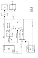
- FIG. 2 is a simplified block diagram of the memory addressing arrangement in a microcomputer system embodying the present invention.
- the system comprises a microprocessor 20, which may be of the type 8088 manufactured by Intel Corporation.
- a microprocessor 20 which may be of the type 8088 manufactured by Intel Corporation.
- DO-7 data input/output terminals
- the DO-7 terminals have been shown separately from the address outputs, though in the 8088 they are commonned with the AO-7 address outputs and time multiplexed.
- a CRT controller system shown at 21, which may contain a type 6845 CRT controller manufactured by Motorola Inc. and additional memory control circuitry, only two of the outputs are shown.
- a random access (RAM)memory 22, of 128K byte capacity and two read-only (ROS) memories, collectively 23, are connected to be addressed by an address system 24.
- the inputs to address system 24 comprise either seventeen bits for a CPU access cycle or a further seventeen bits for a CRT access cycle.
- these address bits comprise fourteen bits, AO through A13, from the CPU address outputs over bus 26 and three bits, the highest order bits, comprising either the CPU A14, A15 and A16 bits, or CPU page bits P0, P1 and P2, from a multiplexer 27 over a bus 28.
- the seventeen address bits to multiplexer 24 comprise bits MAO through MA13 from CRT controller 21 over a bus 29 and CRT page bits P0, P1 and P2, from a page register system 30 over a bus 31.
- Memory paging is controlled by CPU 20 by delivering page bits to page register system 30 over the CPU data bus 36. Only six of the data lines are used for this purpose, and, therefore, six page bits, three for the CPU and three for the CRT are registered. Ignoring, for the moment, the operation of multiplexer 27, by assuming that CPU page bits PO through P2 pass through it from register 30, we will now look at the paging operation.
- address bits AO through A13 are passed from the CPU directly to address system 24 and, with the CRT/not CPU signal from CRT controller in its lowered state, CPU paging bits PO through P2 are applied from register 30 through multiplexer 27 to address system 24 through busses 31 and 28.
- the location in the memory is therefore selected by a 16K byte page area determined by CPU page bits PO through P2 and, within that area, by the fourteen CPU address bits AO through A13.
- a similar operation occurs for each CRT cycle, except that the address bits MAO through MA13 from CRT controller 21 and the CRT page bits PO through P2 are used. These latter bits are read from register system 30 when the CRT/not CPU line from controller 21 is high.
- both CPU 20 and CRT controller 21 have access to any page in memory 22 in accordance with the page bits. These page bits can be changed by the CPU at any time.
- circuits including a decoder 42 and the multiplexer 27 in Figure 2 are operable to decode the video decode addresses shown in Figure 1 and to control ROS addressing.
- the operation of this system is based on the fact that each of the video decode and ROS addresses requires twenty bits. Thus, for the video decode locations (B8000 through BFFFF) the uppermost address bits A16 through A19 are 1101. Similarly, for the ROS addresses (DOOOO through FFFFF) bits A16 through A19 are from 1011 through 1111.
- Decoder 42 which may be in the form of a small ROM decoder, takes bits A16 through A19 from the CPU over a bus 34. If the inputs correspond to the video decode addresses, that is 1101, then output lines 37 and 39 are activated. If the inputs correspond to the ROM addresses (i.e. bits A18 and A19 are both '1') then line 38 is activated. In the latter case, the ROM's 23 are enabled, by the ROM CS (ROM chip select) signal, and the ROM's are addressed from the AO through A17 CPU address outputs.
- ROM CS ROM chip select
- the RA M .CS signal on line 39 enables memory 22 and the signal on line 37 switches multiplexer 27 to pass the CPU A14 through A16 address bits to address memories 22 and 23 instead of CPU page bits PO through P2 during a CPU access cycle.
- This allows direct access to memory 22 from locations 00000 (hex) to 1FFFF (hex) without the paging.
- these video decode addresses are generated by the CPU in order to achieve program compatibility with a larger machine having a dedicated video RAM with these addresses.
- the Figure 2 system provides addresses in memories 22 and 23 using only the A0 through A16 bits from the CPU.
- only line 39 is activated to enable memory 22 for for access using the AO-13 and CPU PO-2 bits at the MAO-13 and CRT PO-2 bits as has been described above.
- a main memory paging system for a microcomputer which is highly flexible and allows access to all pages in the memory by both the CPU and the CRT display subsystem.
- a decoding system permits the use of CPU output addresses higher than the highest address in the main memory either for addressing ROS or for providing automatic access to the main memory for selected ones of these higher addresses to enter video data. This ensures compatibility with higher level machines with greater memory capacity.
Landscapes
- Engineering & Computer Science (AREA)
- Theoretical Computer Science (AREA)
- Physics & Mathematics (AREA)
- General Engineering & Computer Science (AREA)
- General Physics & Mathematics (AREA)
- Digital Computer Display Output (AREA)
- Memory System Of A Hierarchy Structure (AREA)
- Controls And Circuits For Display Device (AREA)
Abstract
Description
- The present invention relates to a microprocessor system including a shared paging memory and is directed to removing any inherent fixed allocation of memory pages to particular users.
- Microcomputer systems presently marketed employ two systems for video data storage. The larger types have a separate video random access memory (RAM) for storing CRT refresh data. In these systems, of course, updating of the video data and reading of this data is effected by access to the dedicated video memory.
- In smaller systems having only a limited RAM capacity, the main store of the system has to hold both video data and the remaining data for processing. In all of such smaller systems without a separate video store, to our knowledge, a small portion of the main store is allocated for display data and is dedicated to this purpose and no other. This has two disadvantages. Firstly the amount of video data for display is severely limited, thereby limiting the display definition. Secondly, as the remaining data can not encroach upon the video area, this area can not be used for other processing operations when the display is not being used.
- It is, therefore, an object of the present invention to provide a memory paging system in a microcomputer which permits flexible allocation of storage space for video and CPU data.
- The present invention provides a microcomputer system including a main memory (22), a central processor unit (20) and a CRT controller (21) for digital display control, characterised in that a paging system, providing high order address bits to define fixed size pages within the main memory, is incorporated, the paging system including a page register system (30) coupled to the data output (36) of the CPU to register both CPU and CRT controller page address bits, and address means (24), responsive thereto, to combine the CPU page address bits with lower order address bits from the CPU address output for CPU access to the memory and the CRT page address bits with lower order address bits from the CRT controller address output for CRT controller access to the memory, whereby both the CPU and the CRT controller can access any page in the memory in accordance with the values of the page address bits placed in the paging register system by the CPU. Thus, there has been added, to a microcomputer, a memory paging system for allocating memory pages to the CPU and to the video subsystem so that both can access any of the main memory pages of the microcomputer under control of the CPU.
- The present invention will be described further by way of example with reference to an embodiment of the invention as illustrated in the accompanying drawings, in which
- Figure 1 is a memory address map showing addresses of main memory, video decode addresses and read-only memory addresses in a microcomputer system; and
- Figure 2 is a block diagram of the memory address system of that microcomputer system.
- The memory map of Figure 1 shows the address ranges of the memories in a microcomputer system. The addresses are shown in hexadecimal notation. The main computer random access memory (RAM) extends from
address 00000 through 1FFFF (128K bytes) and is divided into 8 pages, each of 16K bytes. There are two read-only stores (ROS), one of 128K bytes extending from addresses D0000 through EFFFF, the second of 64K bytes located at addresses FOOOO through FFFFF. Between the RAM and ROS addresses, a video decode area of 32K bytes extending between addresses B8000 and COOOO is shown. As will be explained in more detail later, this is not an actual storage area, but relates to CPU entered addresses which are decoded into addresses in the RAM area. - It should be noted that 16K locations in a page are addressed by fourteen bits (hexadecimal 0000 through 3FFF, thus, for the RAM, three high order bits can be used to define the eight different pages. In accordance with the present invention, these page bits may be used to address the RAM for CPU access and access by a video display subsystem. The CPU uses one page select system and the video display subsystem uses another, the CRT page select system. Both, of course, are controlled by the CPU. The arrangement is such that either the CPU or the video subsystem can employ any single page in the RAM or any number of pages therein up to the full eight pages. At any one time, the CRT page select system will be selecting one page for reading data for display while the CPU page select system will be selecting another page to enter display data into that page. When it is required to change large amounts of data in successive frames, four pages may be required. In such a case, when the display data is to be changed, at the frame flyback time of the display, the page select systems can be switched so that the displayed data is that written in from the CPU during the previous display frame. This feature can be very useful in producing animated displays.
- Turning back to the video decode area shown at locations B8000 through COOO in Figure 1, it is clear that, with a RAM size of 128K bytes (
addresses 00000 through 1FFFF), these high address locations do not exist in RAM. However, there is a situation in which these addresses are generated by the C.P.U. This is when compatibility is required for a series of systems and in the higher level systems certain features are contained in high address locations, which can not be accommodated in the smaller systems with smaller RAM's. As an example, we may assume that the present system is a low level system in a series of microcomputers in which the higher level machines contain a separate video RAM. In the higher level machines, this video RAM is addressed by the CPU and CRT subsystem at addresses B8000 (736K) through BBFFF (752K) to provide 16K bytes of video data. For the smaller machine to remain compatible, the CPU must either convert these addresses to suitable addresses within the range of the RAM or alternatively, in accordance with the present invention, employ these addresses in the same way as the higher level machine, with page conversion outside the CPU. As will be seen in the following description of the Figure 2 system, decoding means is employed to detect these high video addresses and to page them into the available RAM addresses. - Referring now to Figure 2 in detail, this figure is a simplified block diagram of the memory addressing arrangement in a microcomputer system embodying the present invention. The system comprises a
microprocessor 20, which may be of the type 8088 manufactured by Intel Corporation. For simplicity, only the address outputs AO-19 and data input/output terminals DO-7 have been shown. In addition, again for simplicity, the DO-7 terminals have been shown separately from the address outputs, though in the 8088 they are commonned with the AO-7 address outputs and time multiplexed. In a CRT controller system, shown at 21, which may contain a type 6845 CRT controller manufactured by Motorola Inc. and additional memory control circuitry, only two of the outputs are shown. These are the memory address outputs MAO-13 and a CRT/not CPU output. A random access (RAM)memory 22, of 128K byte capacity and two read-only (ROS) memories, collectively 23, are connected to be addressed by anaddress system 24. The inputs to addresssystem 24 comprise either seventeen bits for a CPU access cycle or a further seventeen bits for a CRT access cycle. For each CPU cycle, these address bits comprise fourteen bits, AO through A13, from the CPU address outputs overbus 26 and three bits, the highest order bits, comprising either the CPU A14, A15 and A16 bits, or CPU page bits P0, P1 and P2, from amultiplexer 27 over abus 28. For the CRT cycles, the seventeen address bits tomultiplexer 24 comprise bits MAO through MA13 fromCRT controller 21 over a bus 29 and CRT page bits P0, P1 and P2, from apage register system 30 over abus 31. - Memory paging is controlled by
CPU 20 by delivering page bits topage register system 30 over theCPU data bus 36. Only six of the data lines are used for this purpose, and, therefore, six page bits, three for the CPU and three for the CRT are registered. Ignoring, for the moment, the operation ofmultiplexer 27, by assuming that CPU page bits PO through P2 pass through it from register 30, we will now look at the paging operation. In a CPU cycle, address bits AO through A13 are passed from the CPU directly toaddress system 24 and, with the CRT/not CPU signal from CRT controller in its lowered state, CPU paging bits PO through P2 are applied fromregister 30 throughmultiplexer 27 to addresssystem 24 throughbusses CRT controller 21 and the CRT page bits PO through P2 are used. These latter bits are read fromregister system 30 when the CRT/not CPU line fromcontroller 21 is high. Thus, bothCPU 20 andCRT controller 21 have access to any page inmemory 22 in accordance with the page bits. These page bits can be changed by the CPU at any time. - Turning now to the circuits including a
decoder 42 and themultiplexer 27 in Figure 2, these circuits are operable to decode the video decode addresses shown in Figure 1 and to control ROS addressing. The operation of this system is based on the fact that each of the video decode and ROS addresses requires twenty bits. Thus, for the video decode locations (B8000 through BFFFF) the uppermost address bits A16 through A19 are 1101. Similarly, for the ROS addresses (DOOOO through FFFFF) bits A16 through A19 are from 1011 through 1111. -
Decoder 42, which may be in the form of a small ROM decoder, takes bits A16 through A19 from the CPU over abus 34. If the inputs correspond to the video decode addresses, that is 1101, thenoutput lines 37 and 39 are activated. If the inputs correspond to the ROM addresses (i.e. bits A18 and A19 are both '1') thenline 38 is activated. In the latter case, the ROM's 23 are enabled, by the ROM CS (ROM chip select) signal, and the ROM's are addressed from the AO through A17 CPU address outputs. In the former case, the RAM .CS signal on line 39 enablesmemory 22 and the signal online 37switches multiplexer 27 to pass the CPU A14 through A16 address bits to addressmemories memory 22 from locations 00000 (hex) to 1FFFF (hex) without the paging. It will be remembered that these video decode addresses are generated by the CPU in order to achieve program compatibility with a larger machine having a dedicated video RAM with these addresses. As has been seen, in response to these addresses, the Figure 2 system provides addresses inmemories memory 22 for for access using the AO-13 and CPU PO-2 bits at the MAO-13 and CRT PO-2 bits as has been described above. - In summary, what has been shown is a main memory paging system for a microcomputer which is highly flexible and allows access to all pages in the memory by both the CPU and the CRT display subsystem. In addition, a decoding system permits the use of CPU output addresses higher than the highest address in the main memory either for addressing ROS or for providing automatic access to the main memory for selected ones of these higher addresses to enter video data. This ensures compatibility with higher level machines with greater memory capacity.
- While the invention has been shown and described with reference to one embodiment thereof, it will be understood by those skilled in the art that various changes in form and detail may be made without departing from the scope of the invention, as defined in the following claims.
Claims (6)
Priority Applications (1)
| Application Number | Priority Date | Filing Date | Title |
|---|---|---|---|
| AT84107805T ATE57028T1 (en) | 1983-08-12 | 1984-07-05 | MICROPROCESSOR ARRANGEMENT WITH A SHARED PAGE MEMORY. |
Applications Claiming Priority (2)
| Application Number | Priority Date | Filing Date | Title |
|---|---|---|---|
| US06/522,892 US4608632A (en) | 1983-08-12 | 1983-08-12 | Memory paging system in a microcomputer |
| US522892 | 1995-09-01 |
Publications (3)
| Publication Number | Publication Date |
|---|---|
| EP0134969A2 true EP0134969A2 (en) | 1985-03-27 |
| EP0134969A3 EP0134969A3 (en) | 1988-01-20 |
| EP0134969B1 EP0134969B1 (en) | 1990-09-26 |
Family
ID=24082806
Family Applications (1)
| Application Number | Title | Priority Date | Filing Date |
|---|---|---|---|
| EP84107805A Expired - Lifetime EP0134969B1 (en) | 1983-08-12 | 1984-07-05 | A microprocessor system including a shared paging memory |
Country Status (14)
| Country | Link |
|---|---|
| US (1) | US4608632A (en) |
| EP (1) | EP0134969B1 (en) |
| JP (1) | JPS6034648U (en) |
| KR (1) | KR890002469B1 (en) |
| AR (1) | AR246634A1 (en) |
| AT (1) | ATE57028T1 (en) |
| AU (1) | AU569312B2 (en) |
| BR (1) | BR8403981A (en) |
| CA (1) | CA1216955A (en) |
| DE (1) | DE3483293D1 (en) |
| ES (1) | ES8606689A1 (en) |
| HK (1) | HK10791A (en) |
| MX (1) | MX155254A (en) |
| SG (1) | SG2791G (en) |
Cited By (2)
| Publication number | Priority date | Publication date | Assignee | Title |
|---|---|---|---|---|
| EP0307649A2 (en) * | 1987-08-19 | 1989-03-22 | Compaq Computer Corporation | Data processing system for utilizing a memory-mapped coprocessor within a limited address space |
| EP0318259A2 (en) * | 1987-11-24 | 1989-05-31 | Digital Equipment Corporation | Software configurable memory architecture for data processing system having graphics capability |
Families Citing this family (15)
| Publication number | Priority date | Publication date | Assignee | Title |
|---|---|---|---|---|
| US4608632A (en) * | 1983-08-12 | 1986-08-26 | International Business Machines Corporation | Memory paging system in a microcomputer |
| US4744046A (en) * | 1984-11-02 | 1988-05-10 | Zenith Electronics Corporation | Video display terminal with paging and scrolling |
| EP0205692B1 (en) * | 1985-06-18 | 1991-10-16 | International Business Machines Corporation | Improvements in microprocessors |
| US5201039A (en) * | 1987-09-30 | 1993-04-06 | Mitsubishi Denki Kabushiki Kaisha | Multiple address-space data processor with addressable register and context switching |
| US5148516A (en) * | 1988-08-30 | 1992-09-15 | Hewlett-Packard Company | Efficient computer terminal system utilizing a single slave processor |
| GB9027678D0 (en) * | 1990-12-20 | 1991-02-13 | Ncr Co | Videographics display system |
| IT1254937B (en) * | 1991-05-06 | 1995-10-11 | DYNAMIC UPDATE OF NON-VOLATILE MEMORY IN A COMPUTER SYSTEM | |
| DE4215063C2 (en) * | 1991-05-10 | 1999-11-25 | Intel Corp | Device and method for changing pages in a non-volatile memory |
| WO1995015528A1 (en) * | 1993-11-30 | 1995-06-08 | Vlsi Technology, Inc. | A reallocatable memory subsystem enabling transparent transfer of memory function during upgrade |
| US5822581A (en) * | 1995-09-29 | 1998-10-13 | Intel Corporation | Method for CMOS configuration information storage and retrieval in flash |
| US5930504A (en) * | 1996-07-22 | 1999-07-27 | Intel Corporation | Dynamic nonvolatile memory update in a computer system |
| US6496916B1 (en) * | 1998-04-17 | 2002-12-17 | Agere Systems Inc. | System for flexible memory paging in partitioning memory |
| KR100329768B1 (en) * | 1998-12-30 | 2002-05-09 | 박종섭 | Memory addressing device for micro-controller unit |
| US9535828B1 (en) * | 2013-04-29 | 2017-01-03 | Amazon Technologies, Inc. | Leveraging non-volatile memory for persisting data |
| US11112777B2 (en) * | 2019-03-29 | 2021-09-07 | China Petroleum & Chemical Corporation | Independent high-speed sampling for an oil drilling system |
Citations (2)
| Publication number | Priority date | Publication date | Assignee | Title |
|---|---|---|---|---|
| EP0057815A2 (en) * | 1981-02-05 | 1982-08-18 | International Business Machines Corporation | Page addressing mechanism and method for using the same |
| US4394650A (en) * | 1981-02-19 | 1983-07-19 | Honeywell Information Systems Inc. | Graphic and data character video display system |
Family Cites Families (16)
| Publication number | Priority date | Publication date | Assignee | Title |
|---|---|---|---|---|
| JPS5444451A (en) * | 1977-09-14 | 1979-04-07 | Fujitsu Ltd | Address extension system |
| JPS5454536A (en) * | 1977-10-08 | 1979-04-28 | Fujitsu Ltd | Data processor |
| JPS6041769B2 (en) * | 1977-10-31 | 1985-09-18 | 日本電気株式会社 | Addressing method |
| JPS5474632A (en) * | 1977-11-28 | 1979-06-14 | Nec Corp | Data processor |
| US4500956A (en) * | 1978-07-21 | 1985-02-19 | Tandy Corporation | Memory addressing system |
| JPS5947336B2 (en) * | 1979-03-06 | 1984-11-19 | 富士通株式会社 | data processing equipment |
| JPS55162163A (en) * | 1979-06-04 | 1980-12-17 | Fujitsu Ltd | Address extension system |
| US4342991A (en) * | 1980-03-10 | 1982-08-03 | Multisonics, Inc. | Partial scrolling video generator |
| US4346441A (en) * | 1980-04-29 | 1982-08-24 | Honeywell Information Systems Inc. | Random access memory system for extending the memory addressing capacity of a CPU |
| US4503491A (en) * | 1981-06-29 | 1985-03-05 | Matsushita Electric Industrial Co., Ltd. | Computer with expanded addressing capability |
| US4475176A (en) * | 1981-08-06 | 1984-10-02 | Tokyo Shibaura Denki Kabushiki Kaisha | Memory control system |
| US4429306A (en) * | 1981-09-11 | 1984-01-31 | International Business Machines Corporation | Addressing system for a multiple language character generator |
| US4482979A (en) * | 1982-02-04 | 1984-11-13 | May George A | Video computing system with automatically refreshed memory |
| US4511965A (en) * | 1983-03-21 | 1985-04-16 | Zenith Electronics Corporation | Video ram accessing system |
| US4500961A (en) * | 1983-06-03 | 1985-02-19 | Motorola, Inc. | Page mode memory system |
| US4608632A (en) * | 1983-08-12 | 1986-08-26 | International Business Machines Corporation | Memory paging system in a microcomputer |
-
1983
- 1983-08-12 US US06/522,892 patent/US4608632A/en not_active Expired - Lifetime
-
1984
- 1984-05-10 MX MX201308A patent/MX155254A/en unknown
- 1984-05-16 JP JP1984070472U patent/JPS6034648U/en active Granted
- 1984-07-05 AT AT84107805T patent/ATE57028T1/en not_active IP Right Cessation
- 1984-07-05 DE DE8484107805T patent/DE3483293D1/en not_active Expired - Fee Related
- 1984-07-05 EP EP84107805A patent/EP0134969B1/en not_active Expired - Lifetime
- 1984-07-06 CA CA000458371A patent/CA1216955A/en not_active Expired
- 1984-07-10 KR KR1019840004006A patent/KR890002469B1/en not_active IP Right Cessation
- 1984-08-01 AU AU31372/84A patent/AU569312B2/en not_active Ceased
- 1984-08-02 AR AR84297449A patent/AR246634A1/en active
- 1984-08-09 BR BR8403981A patent/BR8403981A/en not_active IP Right Cessation
- 1984-08-10 ES ES535060A patent/ES8606689A1/en not_active Expired
-
1991
- 1991-01-17 SG SG27/91A patent/SG2791G/en unknown
- 1991-02-06 HK HK107/91A patent/HK10791A/en unknown
Patent Citations (2)
| Publication number | Priority date | Publication date | Assignee | Title |
|---|---|---|---|---|
| EP0057815A2 (en) * | 1981-02-05 | 1982-08-18 | International Business Machines Corporation | Page addressing mechanism and method for using the same |
| US4394650A (en) * | 1981-02-19 | 1983-07-19 | Honeywell Information Systems Inc. | Graphic and data character video display system |
Non-Patent Citations (1)
| Title |
|---|
| ELECTRONIQUE ET APPLICATIONS INDUSTRIELLES, vol. 261, 1st December 1978, pages 29-31, Paris, FR; J.-C. MATHON: "La banque de données à microprocesseur" * |
Cited By (4)
| Publication number | Priority date | Publication date | Assignee | Title |
|---|---|---|---|---|
| EP0307649A2 (en) * | 1987-08-19 | 1989-03-22 | Compaq Computer Corporation | Data processing system for utilizing a memory-mapped coprocessor within a limited address space |
| EP0307649A3 (en) * | 1987-08-19 | 1990-08-08 | Compaq Computer Corporation | Data processing system for utilizing a memory-mapped coprocessor within a limited address space |
| EP0318259A2 (en) * | 1987-11-24 | 1989-05-31 | Digital Equipment Corporation | Software configurable memory architecture for data processing system having graphics capability |
| EP0318259A3 (en) * | 1987-11-24 | 1991-07-24 | Digital Equipment Corporation | Software configurable memory architecture for data processing system having graphics capability |
Also Published As
| Publication number | Publication date |
|---|---|
| ATE57028T1 (en) | 1990-10-15 |
| SG2791G (en) | 1991-04-05 |
| AU3137284A (en) | 1985-02-14 |
| EP0134969A3 (en) | 1988-01-20 |
| MX155254A (en) | 1988-02-10 |
| DE3483293D1 (en) | 1990-10-31 |
| ES8606689A1 (en) | 1986-04-01 |
| JPS6034648U (en) | 1985-03-09 |
| EP0134969B1 (en) | 1990-09-26 |
| KR850002617A (en) | 1985-05-15 |
| ES535060A0 (en) | 1986-04-01 |
| CA1216955A (en) | 1987-01-20 |
| US4608632A (en) | 1986-08-26 |
| AR246634A1 (en) | 1994-08-31 |
| AU569312B2 (en) | 1988-01-28 |
| HK10791A (en) | 1991-02-13 |
| KR890002469B1 (en) | 1989-07-10 |
| JPH049639Y2 (en) | 1992-03-10 |
| BR8403981A (en) | 1985-07-09 |
Similar Documents
| Publication | Publication Date | Title |
|---|---|---|
| EP0134969B1 (en) | A microprocessor system including a shared paging memory | |
| EP0818731B1 (en) | Memory board, memory access method and memory access device | |
| US4809234A (en) | Memory device including memories having different capacities | |
| US4860252A (en) | Self-adaptive computer memory address allocation system | |
| US4475176A (en) | Memory control system | |
| US4713759A (en) | Memory bank switching apparatus | |
| EP0061324A2 (en) | Computer memory management | |
| KR940001877B1 (en) | Multiprocessor system | |
| US4393443A (en) | Memory mapping system | |
| KR920001281B1 (en) | Information processing apparatus | |
| US5280599A (en) | Computer system with memory expansion function and expansion memory setting method | |
| EP0862761A2 (en) | Data error detection and correction for a shared sram | |
| US6625673B1 (en) | Method for assigning addresses to input/output devices | |
| EP0134968A2 (en) | Memory access system in a computer accommodating an add-on memory | |
| US5117492A (en) | Memory addressing system using first and second address signals and modifying second address responsive predetermined values of first address signal | |
| JPS5827253A (en) | Data processing device | |
| JPH0731523B2 (en) | Programmable controller device | |
| US6430647B1 (en) | Data processing system for use in conjunction with a font card or the like | |
| EP0794534A2 (en) | Refreshing of DRAM memory banks | |
| WO1993004430A1 (en) | Self-configuration of memory addresses for computer memory having multiple memory module types | |
| JPH0251753A (en) | Rom address designating circuit | |
| JPS61145789A (en) | Address allocating circuit | |
| JPH11110984A (en) | Access method for re-writable rom | |
| JPH0368047A (en) | Key access control system | |
| JPH02260050A (en) | Memory extension system |
Legal Events
| Date | Code | Title | Description |
|---|---|---|---|
| PUAI | Public reference made under article 153(3) epc to a published international application that has entered the european phase |
Free format text: ORIGINAL CODE: 0009012 |
|
| 17P | Request for examination filed |
Effective date: 19841123 |
|
| AK | Designated contracting states |
Designated state(s): AT BE CH DE FR GB IT LI NL SE |
|
| PUAL | Search report despatched |
Free format text: ORIGINAL CODE: 0009013 |
|
| AK | Designated contracting states |
Kind code of ref document: A3 Designated state(s): AT BE CH DE FR GB IT LI NL SE |
|
| 17Q | First examination report despatched |
Effective date: 19890529 |
|
| GRAA | (expected) grant |
Free format text: ORIGINAL CODE: 0009210 |
|
| AK | Designated contracting states |
Kind code of ref document: B1 Designated state(s): AT BE CH DE FR GB IT LI NL SE |
|
| PG25 | Lapsed in a contracting state [announced via postgrant information from national office to epo] |
Ref country code: NL Effective date: 19900926 Ref country code: AT Effective date: 19900926 |
|
| REF | Corresponds to: |
Ref document number: 57028 Country of ref document: AT Date of ref document: 19901015 Kind code of ref document: T |
|
| REF | Corresponds to: |
Ref document number: 3483293 Country of ref document: DE Date of ref document: 19901031 |
|
| ET | Fr: translation filed | ||
| ITF | It: translation for a ep patent filed |
Owner name: IBM - DR. ALFREDO BRAVI |
|
| NLV1 | Nl: lapsed or annulled due to failure to fulfill the requirements of art. 29p and 29m of the patents act | ||
| PGFP | Annual fee paid to national office [announced via postgrant information from national office to epo] |
Ref country code: SE Payment date: 19910619 Year of fee payment: 8 |
|
| PLBE | No opposition filed within time limit |
Free format text: ORIGINAL CODE: 0009261 |
|
| STAA | Information on the status of an ep patent application or granted ep patent |
Free format text: STATUS: NO OPPOSITION FILED WITHIN TIME LIMIT |
|
| ITTA | It: last paid annual fee | ||
| 26N | No opposition filed | ||
| PGFP | Annual fee paid to national office [announced via postgrant information from national office to epo] |
Ref country code: CH Payment date: 19911023 Year of fee payment: 8 |
|
| PGFP | Annual fee paid to national office [announced via postgrant information from national office to epo] |
Ref country code: GB Payment date: 19920624 Year of fee payment: 9 |
|
| PGFP | Annual fee paid to national office [announced via postgrant information from national office to epo] |
Ref country code: FR Payment date: 19920630 Year of fee payment: 9 |
|
| PG25 | Lapsed in a contracting state [announced via postgrant information from national office to epo] |
Ref country code: SE Effective date: 19920706 |
|
| PGFP | Annual fee paid to national office [announced via postgrant information from national office to epo] |
Ref country code: BE Payment date: 19920708 Year of fee payment: 9 |
|
| PGFP | Annual fee paid to national office [announced via postgrant information from national office to epo] |
Ref country code: DE Payment date: 19920729 Year of fee payment: 9 |
|
| PG25 | Lapsed in a contracting state [announced via postgrant information from national office to epo] |
Ref country code: LI Effective date: 19920731 Ref country code: CH Effective date: 19920731 |
|
| REG | Reference to a national code |
Ref country code: CH Ref legal event code: PL |
|
| PG25 | Lapsed in a contracting state [announced via postgrant information from national office to epo] |
Ref country code: GB Effective date: 19930705 |
|
| PG25 | Lapsed in a contracting state [announced via postgrant information from national office to epo] |
Ref country code: BE Effective date: 19930731 |
|
| BERE | Be: lapsed |
Owner name: INTERNATIONAL BUSINESS MACHINES CORP. Effective date: 19930731 |
|
| GBPC | Gb: european patent ceased through non-payment of renewal fee |
Effective date: 19930705 |
|
| PG25 | Lapsed in a contracting state [announced via postgrant information from national office to epo] |
Ref country code: FR Effective date: 19940331 |
|
| PG25 | Lapsed in a contracting state [announced via postgrant information from national office to epo] |
Ref country code: DE Effective date: 19940401 |
|
| REG | Reference to a national code |
Ref country code: FR Ref legal event code: ST |
|
| EUG | Se: european patent has lapsed |
Ref document number: 84107805.8 Effective date: 19930204 |