EP0134681B1 - Damping system for micro-deflector - Google Patents
Damping system for micro-deflector Download PDFInfo
- Publication number
- EP0134681B1 EP0134681B1 EP84305055A EP84305055A EP0134681B1 EP 0134681 B1 EP0134681 B1 EP 0134681B1 EP 84305055 A EP84305055 A EP 84305055A EP 84305055 A EP84305055 A EP 84305055A EP 0134681 B1 EP0134681 B1 EP 0134681B1
- Authority
- EP
- European Patent Office
- Prior art keywords
- finger
- potential
- micro
- fingers
- deflector
- Prior art date
- Legal status (The legal status is an assumption and is not a legal conclusion. Google has not performed a legal analysis and makes no representation as to the accuracy of the status listed.)
- Expired
Links
- 238000013016 damping Methods 0.000 title claims description 15
- 230000004044 response Effects 0.000 claims description 9
- 230000010355 oscillation Effects 0.000 claims description 6
- 230000005855 radiation Effects 0.000 claims description 3
- 238000010408 sweeping Methods 0.000 claims 1
- 238000011144 upstream manufacturing Methods 0.000 claims 1
- 238000005452 bending Methods 0.000 description 8
- 101100072702 Drosophila melanogaster defl gene Proteins 0.000 description 7
- 238000011084 recovery Methods 0.000 description 4
- XUIMIQQOPSSXEZ-UHFFFAOYSA-N Silicon Chemical compound [Si] XUIMIQQOPSSXEZ-UHFFFAOYSA-N 0.000 description 3
- 230000006870 function Effects 0.000 description 3
- 230000003993 interaction Effects 0.000 description 3
- 229910052710 silicon Inorganic materials 0.000 description 3
- 239000010703 silicon Substances 0.000 description 3
- VYPSYNLAJGMNEJ-UHFFFAOYSA-N Silicium dioxide Chemical compound O=[Si]=O VYPSYNLAJGMNEJ-UHFFFAOYSA-N 0.000 description 2
- 230000000694 effects Effects 0.000 description 2
- 238000003384 imaging method Methods 0.000 description 2
- 230000007935 neutral effect Effects 0.000 description 2
- 229910052581 Si3N4 Inorganic materials 0.000 description 1
- 230000004075 alteration Effects 0.000 description 1
- 238000003491 array Methods 0.000 description 1
- 230000008859 change Effects 0.000 description 1
- 239000011248 coating agent Substances 0.000 description 1
- 238000000576 coating method Methods 0.000 description 1
- 238000004891 communication Methods 0.000 description 1
- 230000000295 complement effect Effects 0.000 description 1
- 238000010276 construction Methods 0.000 description 1
- 239000013078 crystal Substances 0.000 description 1
- 230000003247 decreasing effect Effects 0.000 description 1
- 230000008021 deposition Effects 0.000 description 1
- 238000001514 detection method Methods 0.000 description 1
- 238000010586 diagram Methods 0.000 description 1
- 230000005670 electromagnetic radiation Effects 0.000 description 1
- 230000004907 flux Effects 0.000 description 1
- 239000011521 glass Substances 0.000 description 1
- 239000000463 material Substances 0.000 description 1
- 238000000034 method Methods 0.000 description 1
- 230000003647 oxidation Effects 0.000 description 1
- 238000007254 oxidation reaction Methods 0.000 description 1
- 238000009304 pastoral farming Methods 0.000 description 1
- 238000002360 preparation method Methods 0.000 description 1
- 235000012239 silicon dioxide Nutrition 0.000 description 1
- 239000000377 silicon dioxide Substances 0.000 description 1
- HQVNEWCFYHHQES-UHFFFAOYSA-N silicon nitride Chemical compound N12[Si]34N5[Si]62N3[Si]51N64 HQVNEWCFYHHQES-UHFFFAOYSA-N 0.000 description 1
Images
Classifications
-
- G—PHYSICS
- G02—OPTICS
- G02B—OPTICAL ELEMENTS, SYSTEMS OR APPARATUS
- G02B26/00—Optical devices or arrangements for the control of light using movable or deformable optical elements
- G02B26/08—Optical devices or arrangements for the control of light using movable or deformable optical elements for controlling the direction of light
- G02B26/0816—Optical devices or arrangements for the control of light using movable or deformable optical elements for controlling the direction of light by means of one or more reflecting elements
-
- G—PHYSICS
- G02—OPTICS
- G02B—OPTICAL ELEMENTS, SYSTEMS OR APPARATUS
- G02B26/00—Optical devices or arrangements for the control of light using movable or deformable optical elements
- G02B26/08—Optical devices or arrangements for the control of light using movable or deformable optical elements for controlling the direction of light
- G02B26/10—Scanning systems
Definitions
- the invention relates to micro-deflectors, and more particularly, to a control for reducing the time required for a micro-deflector to return to an undeflected position.
- Micro-deflectors which basically comprise one or more flexible fingers having a reflective surface which permits the finger to function as a light reflector, find use in many applications.
- One application for example, uses a micro-deflector as a facet tracker in a raster scanning system.
- a linear array of micro-deflectors forms a full width modulator for modulating a sheet-like beam of light in response to a video image signal input.
- the flexible finger or fingers that comprise the micro-deflector bend or deflect in response to the application of an electrical potential. Thus, light striking the finger or fingers is directed into a selected path depending upon the presence or absence of an electrical potential.
- Micro-deflectors are disclosed in IEEE Transactions, Vol. ED-25, No. 10, 1978, p.1241, "Dynamic Micromechanics on Silicon: “Techniques and Devices”, by K. E. Petersen.
- a deflecting potential is selectively applied to individual fingers in accordance with a video image signal input.
- the selective deflection of different ones of the micro-deflector fingers modulates the scanning beam and exposes the recording medium, to create the image represented by the image signals.
- the time interval required for the micro-deflector's finger or fingers to settle back into the undeflected position and to stop vibrating following removal of the electrical potential may be of such duration as to restrict system operating speed.
- the recovery time of the finger may be enhanced by changing the finger's physical parameters, ie, by making the finger thicker, changes of this nature are usually accompanied by underiable side effects. For example, where the thickness of the finger is increased, a consequent step increase in the potential required to bend or deflect the finger is necessary if the requisite deflection is to be obtained within the time constraints of the system.
- the invention relates to an improved system for speeding up the return of a micro-deflector to an undeflected quiescent position in preparation for the next cycle, the micro-deflector including at least one flexible finger having a mirror-like surface for reflecting a beam impinged thereagainst, and a support permitting the finger to deflect in response to the application of an electrical potential thereto whereby the beam striking the finger is reflected in another direction, comprising means to impose an electrical potential" on the finger as the finger is returning to the undeflected position following removal of the deflection potential to dampen oscillations of the finger and speed up return of the finger to the undeflected quiescent position.
- Raster scanner 10 comprises a raster output scanner or ROS type scanner wherein a beam 15 of high intensity radiation, e.g., light, modulated in accordance with image signals, is scanned across a photosensitive record medium 13 to expose the record medium in an image configuration.
- the record medium 13 is depicted as being a photoconductively coated xerographic drum 14 which is rotated (by means not shown) in the direction of arrow 16.
- the record medium 13 should be visualized in the generalized case as being a photosensitive medium which is exposed while advancing in a cross line or line pitch direction relative to the scanning beam (identified by numeral 15-2 herein as will appear).
- Beam 15 is derived from a suitable flux source of electromagnetic radiation such as laser 21.
- the collimated beam 15 of monochromatic radiation generated by laser 21 is impinged on a modulator 12 which modifies the beam 15 in conformance with information contained in image signals input thereto as will appear.
- the modulated beam 15-1 passes through a telecentric telescopic beam expander 18 to facet tracker 20 and from facet tracker 20 through a second telecentric telescopic beam expander 22 to a holographic type scanning deflector 24. From deflector 24, the beam is focused by imaging lens 26 on to the record medium 13.
- Modulator 12 is a total internal reflection (i.e. TIR) type modulator having an electro-optic base or element 27 with plural addressable electrodes 28, 28' distributed in succession across a portion of the elelctro-optic element 27 commensurate with the effective size of beam 15.
- the electrodes 28, 28' are 1-30 urn wide and are on centers which are more or less equidisantly separated to provide a generally uniform interelectrode gap sapcing of 1-30 um.
- Electro-optic element 27 comprises a y-cut crystal of LiNb0 3 for example having optically polished input and output faces 31, 32 at the ends thereof, and optically polished intermediate reflecting surface 33. Interdigited electrodes 28, 28' are engaged with, or at least closely adjacent to, the reflecting surface 33 to couple the electric fringe fields which are created into the electro-optic element 27. Electrodes 28, 28' are coupled across a suitable potential V'through leads 29,30, application of potential V' to electrodes 28, 28' being controlled in response to the image signal content.
- the collimated beam 15 from laser 21 enters the electro-optic element 27 through input face 31 at a grazing angle of incidence relative to the reflecting surface 33.
- Beam 15 is brought to a wedge-shaped focus (by means not shown) at approximately the longitudinal centerline of the reflecting surface 33 where it is totally internally reflected and exits from the electro-optic element 27 through the output face 32. While passing through the electro-optic element 27, the beam 15 is spatially phase front modulated in accordance with the image signal content.
- zero-order beam 15-0 When operated in the Bragg regime (shown in Figure 3), where there is no phase alteration, light entering the electro-optic element 27 at the Bragg angle 63 is undiffracted and emerges as zero-order beam 15-0.
- zero-order beam 15-0 is imaged against a suitable stop 37. Where the voltage V' is applied across the electrodes 28, 28', a phase change occurs and the light is scattered into first-order beam 15-1 which is utilized to expose the recording medium 13.
- electro-optic element 27 may be operated in the Raman-Nath regime.
- Other modulator types such as acousto-optic, or electro-optic, etc., as well as laser diodes, may instead be used.
- first-order beam 15-1 serves as the source of scanning beam 15-2 zero-order beam 15-0 may instead be used. In that circumstance, first oder beam 15 - 1 would be impinged against stop 37.
- Deflector 24 comprises a holographic type deflector with a substantially flat scanning disc 46 having a plurality of grating faces or facets 47 around the outer periphery thereof.
- Scanning disc 46 which is preferably made from glass, is rotated by means of motor 48 in synchronism with movement of drum 14.
- disc 46 is disposed so that the first-order beam 15-1 is incident to the facets 47 thereof at an angle of substantially 45°.
- the diffracted scanning beam 15-2 output by disc 46 exits at a complementary angle
- First-order beam 15-1 passes through beam expanders 18, 22 and facet tracker 20 to deflector 24, expanders 18, 22 serving to provide controlled expansion to the beam 15-1 to impinge a beam of desired spot size onto facets 47 of scanning disc 46.
- facet tracker 20 serves to track the first-order beam 15-1 impinging on facets 47 of scanning disc 46 to maintain the beam spot in predetermined position on the facets 47 of scanning disc 46.
- the first-order beam 15-1 reflected by facets 47 of scanning disc 46 (referred to herein as scanning beam 15-2) is focused by imaging lens 26 to a selected spot in the focal plane proximate the surface of drum 14.
- facet tracker 20 is of the micro-deflector type having a flexible finger 50 preferably comprised of silicon dioxide 51 suitably provided on the surface of a silicon wafer 54 as by deposition, thermal oxidation, etc. Other materials, such as silicon, silicon nitride, etc. may be used.
- a metallic mirror-like reflective coating 53 is provided on the outer surface of finger 50. The portion of wafer 54 below finger 50 is removed, creating a space 55 below finger 50 permitting the free end 50 to deflect as illustrated in Figure 4.
- a lead 60 is provided for applying electrical potential to finger 50 with common or return lead 61 coupled to wafer 54.
- a control circuit identified generally by the numeral 65, is provided for applying deflection or bending potentials via lead 60 to finger 50 of micro-deflector facet tracker 20 in synchronization with the rotation of scanning disc 46 and the sweep of scanning beam 15-2 across the photosensitive record medium 13.
- a suitable source of image signals 67 which may for example comprise a memory, communication channel, and the like, is provided together with a suitable clock, referred to herein as pixel clock 69, the latter providing clock pulses for clocking the image signals from signal source 67 to modulator 12.
- a pair of photocell type sensors identified herein as start-of-scan (SOS) and end-of-scan (EOS) sensors 70, 71 respectively, are provided in the path of scanning beam 15-2 to identify the start and end of the image line on the photosensitive record medium 13.
- the signal outputs of SOS and EOS sensors 70, 71 are input to the control terminals of pixel clock 69 to control starting and stopping of clock 69 in synchronization with the sweep of beam 15-2 across record medium 13.
- the clock pulse output of clock 69 is fed via clock lead 72 to image signal source 67, and to the address counter 75 for a suitable non-volatile memory exemplified here by ROM memory 76 via divide-by-N counter 74.
- the clock pulse output of pixel clock 69 to image signal source 67 clocks image signals to modulator 12.
- Modulator 12 in turn modulates beam 15 in synchronism with scanning of the beam 15-2 across the member 13 by deflector 24.
- finger 50 of micro-deflector facet tracker 20 is bent or deflected in a controlled manner by application of a potential thereto.
- the output of ROM memory 76 is fed to a suitable digital-to-analog converter 80.
- the analog signal output of converter 80 is output to an amplifier 81 where the signal is suitably amplified to provide a potential V (defl) sufficient to cause finger 50 to bend or deflect in a controlled manner, the signal output of amplifier 81 being coupled through OR function gate 84 to lead 60 of facet tracker 20.
- a suitable delay circuit 85 is provided to enable the data input to converter 80 to settle prior to generation of potential V (defl). While a digital based system is illustrated herein, it will be understood that a pure analog control function for applying controlled potentials to finger 50, may instead be used.
- ROM memory 76 The contents of ROM memory 76 are obtained through one or more calibration or test runs made to determine the potential V(defl) required to bend finger 50 by an amount necessary to keep the first-order beam 15-1 centered on the facet 47 of scanning disc 46 during scanning.
- V(defl) start-of-scan
- COS center-of-scan
- EOS end-of-scan
- finger 50 of facet tracker 20 One of the principal requirements of finger 50 of facet tracker 20 is that the finger, following deflection, returns to the undeflected quiescent state prior to start of the next scan line.
- V(defl) in line 60 When the bending potential V(defl) in line 60 is removed from finger 50, finger 50, which can for purposes of explanation be considered as a cantilever beam, behaves like a damped free spring-mass vibratory system. Accordingly, finger 50 will return to the undeflected position over a timer interval, referred to as recovery time Tr herein.
- Recovery time Tr which is defined as the time required for the micro-deflector finger 50 to return from a maximum deflected position (shown by solid lines in Figure 4) to an undeflected quiescent position (the dotted line position of Figure 4) under critical damping conditions, is approximately equal to the finger's natural period of vibration.
- a source of damping potential V (damp), shown here as voltage source 90, is provided, the output of voltage source 90 being coupled through lead 91 and gate 84 to lead 60 of finger 50.
- a timer 94 is provided to control both the start and duration of the damping potential V (damp).
- the signal output of timer 94 is input through lead 95-to the control terminal of voltage source 90.
- Lead 97 couples the output of EOS sensor 71 to the control terminal of timer 94.
- pixel clock 69 is actuated in response to the detection of scanning beam 15-2 by SOS detector 70.
- the clock pulse output 69 actuates image signal source 67 to output a line of image signals to modulator 12 which modulates the beam 15 in accordance therewith to write an image line across the photosensitive record medium 13.
- clock pulses output by pixel clock 69 drive counter 75 which, on reaching predetermined count levels, addresses preset memory locations in ROM 76.
- the resulting control signal output of ROM 76 to digital-to-analog converter 80 provides predetermined bending potentials V (defl) to finger 50 of facet tracker 20. Each predetermined bending potential applied to finger 50 causes finger 50 to bend or deflect by a predetermined amount (examples of which are shown in Figure 2 of the drawings).
- finger 50 reflects the first order scanning beam 15-2 through beam expander 22 onto the facets 47 of the rotating scanning disc 46.
- the point at which the scanning beam 15-1 impinges on a facet 47 of scanning disc 46 changes so that the position of the beam 15-1 against the facet of the scanning disc is in effect tracked along the facet as the facet moves thereby to maintain the substantially centered point at which first-order scanning beam 15-1 impinges against the facet.
- the beam is detected by EOS sensor 71 and the signal from sensor 71 terminates operation of pixel clock 69 and the input of image signals from image signal source 67 to modulator 12. Concurrently, the signal from EOS sensor 71 in line 98 resets counter 75 to terminate the input of a bending potential V (defl) from amplifier 81 to finger 50.
- finger 50 With the bending potential terminated, finger 50 returns to the undeflected position.
- the signal from EOS sensor 71. enables timer 94 which, following a predetermined delay chosen to permit the finger 50 to reach substantially the finger's undeflected position, actuates voltage source 90 to apply a predetermined damping potential V (damp) to finger 50 for a preset interval t' (as illustrated in Figure 7a).
- the damping potential V (damp) quickly and rapidly damps or inhibits any oscillations of finger 50 attending normal return of the finger 50 to the finger undeflected position and readies finger 50 for the next scan line.
- micro-deflector constructions and arrangements incorporating the invention may be readily envisioned, e.g., a micro-deflector based modulator employing a single flexible finger to modulate the scanning beam in accordance with an image signal input, or employing one or more linear arrays of fingers and arranged to modulate across an entire scan line at once in response to an image signal input.
Landscapes
- Physics & Mathematics (AREA)
- General Physics & Mathematics (AREA)
- Optics & Photonics (AREA)
- Mechanical Light Control Or Optical Switches (AREA)
- Facsimile Scanning Arrangements (AREA)
- Mechanical Optical Scanning Systems (AREA)
Description
- The invention relates to micro-deflectors, and more particularly, to a control for reducing the time required for a micro-deflector to return to an undeflected position.
- Micro-deflectors, which basically comprise one or more flexible fingers having a reflective surface which permits the finger to function as a light reflector, find use in many applications. One application, for example, uses a micro-deflector as a facet tracker in a raster scanning system. In yet another use, a linear array of micro-deflectors forms a full width modulator for modulating a sheet-like beam of light in response to a video image signal input. In these and other applications, the flexible finger or fingers that comprise the micro-deflector bend or deflect in response to the application of an electrical potential. Thus, light striking the finger or fingers is directed into a selected path depending upon the presence or absence of an electrical potential.
- Micro-deflectors are disclosed in IEEE Transactions, Vol. ED-25, No. 10, 1978, p.1241, "Dynamic Micromechanics on Silicon: "Techniques and Devices", by K. E. Petersen.
- Where for example a linear micro-deflector array is used, a deflecting potential is selectively applied to individual fingers in accordance with a video image signal input. The selective deflection of different ones of the micro-deflector fingers modulates the scanning beam and exposes the recording medium, to create the image represented by the image signals.
- However, it has been found, particularly in high speed applications, that the time interval required for the micro-deflector's finger or fingers to settle back into the undeflected position and to stop vibrating following removal of the electrical potential may be of such duration as to restrict system operating speed. While the recovery time of the finger may be enhanced by changing the finger's physical parameters, ie, by making the finger thicker, changes of this nature are usually accompanied by underiable side effects. For example, where the thickness of the finger is increased, a consequent step increase in the potential required to bend or deflect the finger is necessary if the requisite deflection is to be obtained within the time constraints of the system. Alternatively, one might consider providing a physical stop or abutment to intercept and stop the finger at the neutral position and settle vibrations. However, stops of this nature may not dampen out all vibrations along the length of the flexible finger and could result in undesirable wear and fatigue of the finger.
- The invention relates to an improved system for speeding up the return of a micro-deflector to an undeflected quiescent position in preparation for the next cycle, the micro-deflector including at least one flexible finger having a mirror-like surface for reflecting a beam impinged thereagainst, and a support permitting the finger to deflect in response to the application of an electrical potential thereto whereby the beam striking the finger is reflected in another direction, comprising means to impose an electrical potential" on the finger as the finger is returning to the undeflected position following removal of the deflection potential to dampen oscillations of the finger and speed up return of the finger to the undeflected quiescent position.
- The invention will now be described by way of example with reference to the accompanying drawings, in which:
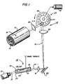
- Figure 1 is a schematic view of the micro-deflector of the present invention embodied in a facet tracker for a raster scanner of the type having a total internal reflection (TIR) modulator and holographic scanning disc;
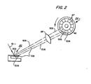
- Figure 2 is a schematic view illustrating the manner in which facet tracking is effected by the facet tracker shown in Figure 1;
- Figure 3 is an enlarged bottom plan view showing details of the TIR modulator for the scanner shown in Figure 1;
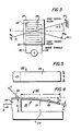
- Figure 4 is an enlarged side view in cross section of the micro-deflector type facet tracker of Figure 1 showing the facet tracker's flexible finger;
- Figure 5 is a top plan view of the flexible finger shown in Figure 4;
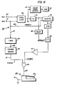
- Figure 6 is a logic diagram showing the control system for the raster scanner of Figure 1 including means to dampen oscillations of the facet tracker flexible finger following removal of the bending potential; and
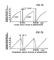
- Figures 7a and 7b are graphical representations. showing the relationship between deflection potential and the rate of deflection of the facet tracker finger.
- Referring, particularly to Figures 1-3 of the drawings, an exemplary raster scanner, designated generally by the
numeral 10, incorporating the micro-deflector of the present invention is there shown. Rasterscanner 10 comprises a raster output scanner or ROS type scanner wherein abeam 15 of high intensity radiation, e.g., light, modulated in accordance with image signals, is scanned across aphotosensitive record medium 13 to expose the record medium in an image configuration. Therecord medium 13 is depicted as being a photoconductively coatedxerographic drum 14 which is rotated (by means not shown) in the direction ofarrow 16. Nevertheless, it will be understood that other xerographic and non-xerographic record media may instead be used, including photoconductively coated xerographic belts and plates, as well as photosensitive film and coated paper in web or cut sheet stock form. Accordingly, therecord medium 13 should be visualized in the generalized case as being a photosensitive medium which is exposed while advancing in a cross line or line pitch direction relative to the scanning beam (identified by numeral 15-2 herein as will appear). - Beam 15 is derived from a suitable flux source of electromagnetic radiation such as
laser 21. The collimatedbeam 15 of monochromatic radiation generated bylaser 21 is impinged on amodulator 12 which modifies thebeam 15 in conformance with information contained in image signals input thereto as will appear. The modulated beam 15-1 passes through a telecentric telescopic beam expander 18 tofacet tracker 20 and fromfacet tracker 20 through a second telecentric telescopic beam expander 22 to a holographictype scanning deflector 24. Fromdeflector 24, the beam is focused byimaging lens 26 on to therecord medium 13. -
Modulator 12 is a total internal reflection (i.e. TIR) type modulator having an electro-optic base orelement 27 with pluraladdressable electrodes 28, 28' distributed in succession across a portion of the elelctro-optic element 27 commensurate with the effective size ofbeam 15. Typically, theelectrodes 28, 28' are 1-30 urn wide and are on centers which are more or less equidisantly separated to provide a generally uniform interelectrode gap sapcing of 1-30 um. - Electro-
optic element 27 comprises a y-cut crystal of LiNb03 for example having optically polished input and output faces 31, 32 at the ends thereof, and optically polished intermediate reflectingsurface 33. Interdigitedelectrodes 28, 28' are engaged with, or at least closely adjacent to, the reflectingsurface 33 to couple the electric fringe fields which are created into the electro-optic element 27.Electrodes 28, 28' are coupled across a suitable potential V'through leads 29,30, application of potential V' toelectrodes 28, 28' being controlled in response to the image signal content. - As can be understood, the collimated
beam 15 fromlaser 21 enters the electro-optic element 27 throughinput face 31 at a grazing angle of incidence relative to the reflectingsurface 33.Beam 15 is brought to a wedge-shaped focus (by means not shown) at approximately the longitudinal centerline of the reflectingsurface 33 where it is totally internally reflected and exits from the electro-optic element 27 through theoutput face 32. While passing through the electro-optic element 27, thebeam 15 is spatially phase front modulated in accordance with the image signal content. - Differences in potential between
electrodes 28, 28' create localized electric fringe fields which penetrate into aninteraction region 39 of the electro-optic element 27 to produce a variation in the element's refractive index widthwise of the interaction region. Consequently, as thebeam 15 is traversing theinteraction region 39, its phase front is sequentially spatially modulated in accordance with the image signal input. - When operated in the Bragg regime (shown in Figure 3), where there is no phase alteration, light entering the electro-
optic element 27 at the Bragg angle 63 is undiffracted and emerges as zero-order beam 15-0. In the example shown, zero-order beam 15-0 is imaged against asuitable stop 37. Where the voltage V' is applied across theelectrodes 28, 28', a phase change occurs and the light is scattered into first-order beam 15-1 which is utilized to expose therecording medium 13. - While a Bragg diffraction regime is illustrated, electro-
optic element 27 may be operated in the Raman-Nath regime. Other modulator types, such as acousto-optic, or electro-optic, etc., as well as laser diodes, may instead be used. While first-order beam 15-1 serves as the source of scanning beam 15-2 zero-order beam 15-0 may instead be used. In that circumstance, first oderbeam 15-1 would be impinged againststop 37. -
Deflector 24 comprises a holographic type deflector with a substantiallyflat scanning disc 46 having a plurality of grating faces orfacets 47 around the outer periphery thereof.Scanning disc 46, which is preferably made from glass, is rotated by means ofmotor 48 in synchronism with movement ofdrum 14. Preferably,disc 46 is disposed so that the first-order beam 15-1 is incident to thefacets 47 thereof at an angle of substantially 45°. The diffracted scanning beam 15-2 output bydisc 46 exits at a complementary angle - First-order beam 15-1 passes through
beam expanders facet tracker 20 todeflector 24, expanders 18, 22 serving to provide controlled expansion to the beam 15-1 to impinge a beam of desired spot size ontofacets 47 ofscanning disc 46. As will appear more fully herein,facet tracker 20 serves to track the first-order beam 15-1 impinging onfacets 47 of scanningdisc 46 to maintain the beam spot in predetermined position on thefacets 47 ofscanning disc 46. The first-order beam 15-1 reflected byfacets 47 of scanning disc 46 (referred to herein as scanning beam 15-2) is focused byimaging lens 26 to a selected spot in the focal plane proximate the surface ofdrum 14. - Referring particularly to Figures 4 and 5 of the drawings,
facet tracker 20 is of the micro-deflector type having aflexible finger 50 preferably comprised ofsilicon dioxide 51 suitably provided on the surface of asilicon wafer 54 as by deposition, thermal oxidation, etc. Other materials, such as silicon, silicon nitride, etc. may be used. A metallic mirror-likereflective coating 53 is provided on the outer surface offinger 50. The portion ofwafer 54 belowfinger 50 is removed, creating aspace 55 belowfinger 50 permitting thefree end 50 to deflect as illustrated in Figure 4. Alead 60 is provided for applying electrical potential tofinger 50 with common orreturn lead 61 coupled to wafer 54. - Referring to Figure 6, a control circuit, identified generally by the numeral 65, is provided for applying deflection or bending potentials via
lead 60 tofinger 50 ofmicro-deflector facet tracker 20 in synchronization with the rotation ofscanning disc 46 and the sweep of scanning beam 15-2 across thephotosensitive record medium 13. A suitable source of image signals 67, which may for example comprise a memory, communication channel, and the like, is provided together with a suitable clock, referred to herein aspixel clock 69, the latter providing clock pulses for clocking the image signals fromsignal source 67 tomodulator 12. A pair of photocell type sensors, identified herein as start-of-scan (SOS) and end-of-scan (EOS)sensors photosensitive record medium 13. The signal outputs of SOS andEOS sensors pixel clock 69 to control starting and stopping ofclock 69 in synchronization with the sweep of beam 15-2 acrossrecord medium 13. The clock pulse output ofclock 69 is fed viaclock lead 72 to imagesignal source 67, and to theaddress counter 75 for a suitable non-volatile memory exemplified here byROM memory 76 via divide-by-N counter 74. As indicated, the clock pulse output ofpixel clock 69 to imagesignal source 67 clocks image signals tomodulator 12.Modulator 12 in turn modulatesbeam 15 in synchronism with scanning of the beam 15-2 across themember 13 bydeflector 24. - To enable the position of the spot where first-order beam 15-1 impinges on the
facets 47 ofscanning disc 46 to be controlled throughout the scan,finger 50 ofmicro-deflector facet tracker 20 is bent or deflected in a controlled manner by application of a potential thereto. For this purpose, the output ofROM memory 76 is fed to a suitable digital-to-analog converter 80. The analog signal output ofconverter 80 is output to an amplifier 81 where the signal is suitably amplified to provide a potential V (defl) sufficient to causefinger 50 to bend or deflect in a controlled manner, the signal output of amplifier 81 being coupled through ORfunction gate 84 to lead 60 offacet tracker 20. Asuitable delay circuit 85 is provided to enable the data input toconverter 80 to settle prior to generation of potential V (defl). While a digital based system is illustrated herein, it will be understood that a pure analog control function for applying controlled potentials tofinger 50, may instead be used. - The contents of
ROM memory 76 are obtained through one or more calibration or test runs made to determine the potential V(defl) required to bendfinger 50 by an amount necessary to keep the first-order beam 15-1 centered on thefacet 47 ofscanning disc 46 during scanning. In Figure 2, the relative positions of the first-order beam 15-1 at start-of-scan (SOS), center-of-scan (COS) and end-of-scan (EOS) in relation to the deflection offinger 50 offacet tracker 20 are illustrated, it being understood that the positions shown are for example only and are not intended to reflect true positions of beam 15-1. - One of the principal requirements of
finger 50 offacet tracker 20 is that the finger, following deflection, returns to the undeflected quiescent state prior to start of the next scan line. When the bending potential V(defl) inline 60 is removed fromfinger 50,finger 50, which can for purposes of explanation be considered as a cantilever beam, behaves like a damped free spring-mass vibratory system. Accordingly,finger 50 will return to the undeflected position over a timer interval, referred to as recovery time Tr herein. - Recovery time Tr, which is defined as the time required for the
micro-deflector finger 50 to return from a maximum deflected position (shown by solid lines in Figure 4) to an undeflected quiescent position (the dotted line position of Figure 4) under critical damping conditions, is approximately equal to the finger's natural period of vibration. Where for example, afinger 50 of the type described has a length L = 160 pm, a width w = 100 pm, a thickness b = 2 p, and depth d = 5 pm, the finger has a natural frequency of approximately 73 kHz with a Q factor = 1.37. If a maximum bending potential V (defl) of 51 volts is applied and then removed,finger 50 would typically oscillate with decreasing amplitude and return to an undeflected quiescent state in a time Tr = 30 µsec. - Referring now particulary to Figure 6, a source of damping potential V (damp), shown here as
voltage source 90, is provided, the output ofvoltage source 90 being coupled throughlead 91 andgate 84 to lead 60 offinger 50. To control both the start and duration of the damping potential V (damp), atimer 94 is provided. The signal output oftimer 94 is input through lead 95-to the control terminal ofvoltage source 90. Lead 97 couples the output ofEOS sensor 71 to the control terminal oftimer 94. - Referring particularly to Figures 1, 2 and 5-7b,
pixel clock 69 is actuated in response to the detection of scanning beam 15-2 bySOS detector 70. Theclock pulse output 69 actuatesimage signal source 67 to output a line of image signals to modulator 12 which modulates thebeam 15 in accordance therewith to write an image line across thephotosensitive record medium 13. Concurrently, clock pulses output bypixel clock 69 drive counter 75 which, on reaching predetermined count levels, addresses preset memory locations inROM 76. The resulting control signal output ofROM 76 to digital-to-analog converter 80 provides predetermined bending potentials V (defl) tofinger 50 offacet tracker 20. Each predetermined bending potential applied tofinger 50 causesfinger 50 to bend or deflect by a predetermined amount (examples of which are shown in Figure 2 of the drawings). - As described,
finger 50 reflects the first order scanning beam 15-2 throughbeam expander 22 onto thefacets 47 of therotating scanning disc 46. Asfinger 50 bends or deflects, the point at which the scanning beam 15-1 impinges on afacet 47 ofscanning disc 46 changes so that the position of the beam 15-1 against the facet of the scanning disc is in effect tracked along the facet as the facet moves thereby to maintain the substantially centered point at which first-order scanning beam 15-1 impinges against the facet. - As the scanning beam 15-2 reaches the end of the scan line, the beam is detected by
EOS sensor 71 and the signal fromsensor 71 terminates operation ofpixel clock 69 and the input of image signals fromimage signal source 67 tomodulator 12. Concurrently, the signal fromEOS sensor 71 in line 98 resets counter 75 to terminate the input of a bending potential V (defl) from amplifier 81 tofinger 50. - With the bending potential terminated,
finger 50 returns to the undeflected position. The signal fromEOS sensor 71. enablestimer 94 which, following a predetermined delay chosen to permit thefinger 50 to reach substantially the finger's undeflected position, actuatesvoltage source 90 to apply a predetermined damping potential V (damp) tofinger 50 for a preset interval t' (as illustrated in Figure 7a). The damping potential V (damp) quickly and rapidly damps or inhibits any oscillations offinger 50 attending normal return of thefinger 50 to the finger undeflected position and readiesfinger 50 for the next scan line. - It has been found that a damping potential V (damp) of 62 volts over a interval t' = 0.25 psec and applied substantially at the time the
finger 50 offacet tracker 20 reaches the undeflected position results in substantially instantaneous damping of any oscillations offinger 50 and returns the finger from a point of maximum deflection to a neutral quiescent state in a recovery time Tr of approximately 5 usec. Other wave forms for dampeningfinger 50 may be used. - Other micro-deflector constructions and arrangements incorporating the invention may be readily envisioned, e.g., a micro-deflector based modulator employing a single flexible finger to modulate the scanning beam in accordance with an image signal input, or employing one or more linear arrays of fingers and arranged to modulate across an entire scan line at once in response to an image signal input.
Claims (6)
Applications Claiming Priority (2)
| Application Number | Priority Date | Filing Date | Title |
|---|---|---|---|
| US06/523,983 US4561023A (en) | 1983-08-16 | 1983-08-16 | Dampening system for micro-deflector scanning beam modulator |
| US523983 | 1983-08-16 |
Publications (2)
| Publication Number | Publication Date |
|---|---|
| EP0134681A1 EP0134681A1 (en) | 1985-03-20 |
| EP0134681B1 true EP0134681B1 (en) | 1987-11-25 |
Family
ID=24087252
Family Applications (1)
| Application Number | Title | Priority Date | Filing Date |
|---|---|---|---|
| EP84305055A Expired EP0134681B1 (en) | 1983-08-16 | 1984-07-25 | Damping system for micro-deflector |
Country Status (4)
| Country | Link |
|---|---|
| US (1) | US4561023A (en) |
| EP (1) | EP0134681B1 (en) |
| JP (1) | JPS6069624A (en) |
| DE (1) | DE3467818D1 (en) |
Families Citing this family (7)
| Publication number | Priority date | Publication date | Assignee | Title |
|---|---|---|---|---|
| DE3636985A1 (en) * | 1985-11-12 | 1987-05-14 | Xerox Corp | COMBINED HOLOGRAFIC SCREEN AND IMAGE ELEMENT CLOCK |
| US5166944A (en) * | 1991-06-07 | 1992-11-24 | Advanced Laser Technologies, Inc. | Laser beam scanning apparatus and method |
| US5153644A (en) * | 1991-08-19 | 1992-10-06 | Xerox Corporation | Dual mode correction of image distortion in a xerographic printing apparatus |
| US6073846A (en) * | 1994-08-17 | 2000-06-13 | Metrologic Instruments, Inc. | Holographic laser scanning system and process and apparatus and method |
| EP1081529A3 (en) * | 1999-08-30 | 2002-05-29 | PSC Scanning, Inc. | Reflective dither spring |
| CN104777136B (en) * | 2015-03-25 | 2018-06-19 | 深圳市贝沃德克生物技术研究院有限公司 | Biological marker object detecting method and system based on surface plasma resonance technology |
| CN104749118B (en) * | 2015-03-25 | 2018-06-19 | 深圳市贝沃德克生物技术研究院有限公司 | Variable intervenes formula biomarker concentration detection method and device |
Family Cites Families (8)
| Publication number | Priority date | Publication date | Assignee | Title |
|---|---|---|---|---|
| US3544201A (en) * | 1968-01-02 | 1970-12-01 | Gen Telephone & Elect | Optical beam deflector |
| FR2224828A1 (en) * | 1973-04-09 | 1974-10-31 | Thomson Brandt | |
| US4368489A (en) * | 1978-07-17 | 1983-01-11 | Agfa-Gevaert Ag | Galvanometer-type tilting-mirror scanning system and circuit therefor |
| US4385798A (en) * | 1980-09-16 | 1983-05-31 | Yevick George J | Piezoelectric light beam deflector |
| US4397521A (en) * | 1980-09-29 | 1983-08-09 | Xerox Corporation | Double pass optical system for raster scanners |
| US4441126A (en) * | 1982-05-06 | 1984-04-03 | Sperry Corporation | Adaptive corrector of facet errors in mirror scanning systems |
| US4454547A (en) * | 1982-07-02 | 1984-06-12 | Xerox Corporation | Raster output scanner having a full width electro-mechanical modulator |
| US4450458A (en) * | 1982-07-02 | 1984-05-22 | Xerox Corporation | Multi-function reproduction apparatus |
-
1983
- 1983-08-16 US US06/523,983 patent/US4561023A/en not_active Expired - Fee Related
-
1984
- 1984-07-25 DE DE8484305055T patent/DE3467818D1/en not_active Expired
- 1984-07-25 EP EP84305055A patent/EP0134681B1/en not_active Expired
- 1984-08-09 JP JP59167267A patent/JPS6069624A/en active Granted
Also Published As
| Publication number | Publication date |
|---|---|
| JPH057689B2 (en) | 1993-01-29 |
| EP0134681A1 (en) | 1985-03-20 |
| JPS6069624A (en) | 1985-04-20 |
| US4561023A (en) | 1985-12-24 |
| DE3467818D1 (en) | 1988-01-07 |
Similar Documents
| Publication | Publication Date | Title |
|---|---|---|
| EP0155844B1 (en) | Pulse imaging system | |
| US4205348A (en) | Laser scanning utilizing facet tracking and acousto pulse imaging techniques | |
| US4686542A (en) | High speed, high resolution raster output scanner | |
| US4213158A (en) | Optical data recording system utilizing acoustic pulse imaging to minimize image blur | |
| US4170028A (en) | Facet tracking in laser scanning | |
| US4386827A (en) | Electrooptical scanning device | |
| EP0020930B1 (en) | An acousto-optically modulated scanning system | |
| US4321564A (en) | Sequential beam switching of acousto-optic modulator | |
| US4602852A (en) | Acousto-optic deflector systems | |
| EP0299964B1 (en) | Scanning apparatus | |
| US4577933A (en) | Gap modulator for high speed scanners | |
| CA1214493A (en) | Multi-channel electro-optic printer | |
| US4307409A (en) | Multi-aperture, feedback system for a laser scanner | |
| EP0134681B1 (en) | Damping system for micro-deflector | |
| US4559562A (en) | Microdeflector facet tracker for scanning system | |
| US4751525A (en) | Scanning system and method of scanning | |
| US3964032A (en) | Optical system for storing information | |
| US4961632A (en) | Light beam deflector/modulator | |
| CA1186237A (en) | Printer beam position feedback sensor | |
| US4780732A (en) | Dual interaction TIR modulator | |
| US3985426A (en) | Light beam deflection resolution amplifier means | |
| JPS6137606B2 (en) | ||
| EP0490013A1 (en) | Electro-optical scanner | |
| JP3435219B2 (en) | Optical scanning device | |
| JPS61147220A (en) | Light beam scannin device |
Legal Events
| Date | Code | Title | Description |
|---|---|---|---|
| PUAI | Public reference made under article 153(3) epc to a published international application that has entered the european phase |
Free format text: ORIGINAL CODE: 0009012 |
|
| AK | Designated contracting states |
Designated state(s): DE FR GB |
|
| 17P | Request for examination filed |
Effective date: 19850706 |
|
| 17Q | First examination report despatched |
Effective date: 19860910 |
|
| GRAA | (expected) grant |
Free format text: ORIGINAL CODE: 0009210 |
|
| AK | Designated contracting states |
Kind code of ref document: B1 Designated state(s): DE FR GB |
|
| REF | Corresponds to: |
Ref document number: 3467818 Country of ref document: DE Date of ref document: 19880107 |
|
| ET | Fr: translation filed | ||
| PLBE | No opposition filed within time limit |
Free format text: ORIGINAL CODE: 0009261 |
|
| STAA | Information on the status of an ep patent application or granted ep patent |
Free format text: STATUS: NO OPPOSITION FILED WITHIN TIME LIMIT |
|
| 26N | No opposition filed | ||
| PGFP | Annual fee paid to national office [announced via postgrant information from national office to epo] |
Ref country code: FR Payment date: 19960709 Year of fee payment: 13 |
|
| PGFP | Annual fee paid to national office [announced via postgrant information from national office to epo] |
Ref country code: GB Payment date: 19960716 Year of fee payment: 13 |
|
| PGFP | Annual fee paid to national office [announced via postgrant information from national office to epo] |
Ref country code: DE Payment date: 19960802 Year of fee payment: 13 |
|
| PG25 | Lapsed in a contracting state [announced via postgrant information from national office to epo] |
Ref country code: GB Free format text: LAPSE BECAUSE OF NON-PAYMENT OF DUE FEES Effective date: 19970725 |
|
| GBPC | Gb: european patent ceased through non-payment of renewal fee |
Effective date: 19970725 |
|
| PG25 | Lapsed in a contracting state [announced via postgrant information from national office to epo] |
Ref country code: FR Free format text: LAPSE BECAUSE OF NON-PAYMENT OF DUE FEES Effective date: 19980331 |
|
| PG25 | Lapsed in a contracting state [announced via postgrant information from national office to epo] |
Ref country code: DE Free format text: LAPSE BECAUSE OF NON-PAYMENT OF DUE FEES Effective date: 19980401 |
|
| REG | Reference to a national code |
Ref country code: FR Ref legal event code: ST |