EP0133344A2 - System for displaying alphanumeric messages - Google Patents
System for displaying alphanumeric messages Download PDFInfo
- Publication number
- EP0133344A2 EP0133344A2 EP84304457A EP84304457A EP0133344A2 EP 0133344 A2 EP0133344 A2 EP 0133344A2 EP 84304457 A EP84304457 A EP 84304457A EP 84304457 A EP84304457 A EP 84304457A EP 0133344 A2 EP0133344 A2 EP 0133344A2
- Authority
- EP
- European Patent Office
- Prior art keywords
- message
- signal
- character
- display
- real time
- Prior art date
- Legal status (The legal status is an assumption and is not a legal conclusion. Google has not performed a legal analysis and makes no representation as to the accuracy of the status listed.)
- Granted
Links
- 230000000007 visual effect Effects 0.000 claims abstract description 27
- 230000004044 response Effects 0.000 claims description 9
- 230000004913 activation Effects 0.000 claims description 7
- 230000003213 activating effect Effects 0.000 claims 2
- 239000004020 conductor Substances 0.000 description 22
- 230000001143 conditioned effect Effects 0.000 description 3
- 238000001514 detection method Methods 0.000 description 3
- 238000010586 diagram Methods 0.000 description 3
- 238000004519 manufacturing process Methods 0.000 description 2
- 230000005540 biological transmission Effects 0.000 description 1
- 239000003990 capacitor Substances 0.000 description 1
- 230000003750 conditioning effect Effects 0.000 description 1
- 230000006870 function Effects 0.000 description 1
- 230000007274 generation of a signal involved in cell-cell signaling Effects 0.000 description 1
- 238000007689 inspection Methods 0.000 description 1
- 239000000463 material Substances 0.000 description 1
- 230000007246 mechanism Effects 0.000 description 1
- 230000004048 modification Effects 0.000 description 1
- 238000012986 modification Methods 0.000 description 1
- 238000012544 monitoring process Methods 0.000 description 1
- 230000000063 preceeding effect Effects 0.000 description 1
- 230000001105 regulatory effect Effects 0.000 description 1
- 239000000126 substance Substances 0.000 description 1
- 238000006467 substitution reaction Methods 0.000 description 1
Images

Classifications
-
- G—PHYSICS
- G06—COMPUTING; CALCULATING OR COUNTING
- G06F—ELECTRIC DIGITAL DATA PROCESSING
- G06F3/00—Input arrangements for transferring data to be processed into a form capable of being handled by the computer; Output arrangements for transferring data from processing unit to output unit, e.g. interface arrangements
- G06F3/14—Digital output to display device ; Cooperation and interconnection of the display device with other functional units
- G06F3/147—Digital output to display device ; Cooperation and interconnection of the display device with other functional units using display panels
-
- G—PHYSICS
- G09—EDUCATION; CRYPTOGRAPHY; DISPLAY; ADVERTISING; SEALS
- G09G—ARRANGEMENTS OR CIRCUITS FOR CONTROL OF INDICATING DEVICES USING STATIC MEANS TO PRESENT VARIABLE INFORMATION
- G09G3/00—Control arrangements or circuits, of interest only in connection with visual indicators other than cathode-ray tubes
- G09G3/04—Control arrangements or circuits, of interest only in connection with visual indicators other than cathode-ray tubes for presentation of a single character by selection from a plurality of characters, or by composing the character by combination of individual elements, e.g. segments using a combination of such display devices for composing words, rows or the like, in a frame with fixed character positions
Definitions
- This invention relates to a system for displaying alphanumeric messages by means of a unitary visual display device and deals more particularly with apparatus for expanding the message display capacity of such a device.
- Multiple character station unitary visual display devices used in display systems are generally well known in the art. Such multiple character display devices generally have a fixed number of character stations which limit the number of characters in the displayed message to the number of character display stations of the device.
- One such display system employing a limited capacity multiple character station device is illustrated and described in U.S. Patent No. 4,381,505 assigned to the assignee of the present invention.
- the controller may operate to select a message unit from a memory in accordance with different conditions monitored by the controller which when displayed advises an operator of a monitored condition, provides a warning, gives an instruction or the like, or the controller may also select a stored message component from the memory to which is added real time data representing the value of real time variables or other associated real time conditions.
- a limitation in displaying multiple-message unit messages in a unitary visual display device system is generally the expense and complexity associated with the additional equipment such as memory modules and software programming in the controller operating with such a display system.
- BCD binary coded decimal
- Still another limitation is the additional controller equipment and associated software required to provide a reserve signal to the display system to reserve character locations in the visual display device to display real time data associated with a stored message component having a real time message component.
- a unitary visual display system for use with controllers or the like capable of displaying multiple-message unit messages wherein the message units may be made up of entirely stored message units or message units having both stored and real time components and that avoids the drawbacks of the aforedescribed display systems.
- the general aim of the present invention is to provide an improved alphanumeric unitary visual display system having an expanded message display capability that overcomes the limitations of previously used unitary visual display systems.
- the unitary visual display system of the present invention provides multiple-message unit message display capability and real time data reserve signals without the complex hardware, software, and wiring generally required in controllers used with prior display systems.
- the invention resides in a circuit for scrolling message units in an alphanumeric visual display system having a unitary multi-character station limited capacity character display device.
- the message units are stored in a memory means and are made up of a plurality of characters not greater in number than the number of character stations of the display device and each message unit has a predetermined character display signal position.
- Some of the message units are comprised of stored message components and real time message components with the stored message components having a plurality of characters smaller in number than the number of character stations of the display device.
- a real time signal means associated with a plurality of real time conditions provides a selection of real time message components.
- a complete message comprises a single message unit or a number of message units in sequence.
- the invention more specifically resides in a first signal means to indicate the first message unit in a complete message and a first sensing means to detect the presence of the first signal means in a first predetermined character display signal position.
- a scrolling activation circuit means is responsive to the detection of the first signal means and enables a message unit scrolling means circuit so that each message unit of a complete message is automatically accessed and selected from the memory means and displayed in a time-spaced relationship by the visual display device.
- the invention further resides in a second signal means to indicate the last message unit in a complete message and a second sensing means to detect the presence of the second signal means in a second predetermined character display signal position to deactivate the scrolling circuit means.
- the invention also resides in a reserve digit signal means to indicate that a message unit includes a stored message component and a real time message component.
- a third sensing means detects the presence of the reserve digit signal means in a third predetermined character display signal position.
- a reserve character select logic circuit means responsive to the third sensing means reserves a number of character display locations of the visual display device to display in the reserved locations a corresponding number of characters comprising the real time message component.
- a representative system for displaying alphanumeric messages by means of a multi-character station unitary visual display device having a limited capacity character display and capable of embodying the present invention is manufactured by The Arthur G. Russell Company, Incorporated, of Bristol, Connecticut. Briefly, the system has a display device with a row of character stations at each of which a character may be created for display in response to a set of signals applied to the character station.
- a memory device stores a plurality of message units, some of which are complete message units and others of which are stored message components.
- the message units selected by a real time means are converted by a control circuit into a set of signals which are applied in a one to one relationship to the character stations of the display device to cause the display of a single complete message unit.
- the display system is illustrated and described in U.S. Patent No. 4,381,505, issued April 26, 1983 and assigned to the assignee of the present invention.
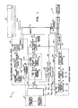
- Fig. 1 shows in block diagram form, an alphanumeric unitary visual display system designated generally by the numeral 8 embodying the invention.
- the display system comprises a multi-character station unitary visual display device 10, a memory means 12 which stores a variety of message units, a real time signal means shown generally at 14 providing a selection of real time message components, a master clock means 16, a reserve digit real time signal means 18 for reserving a plurality of character stations to display a real time message component and a multiple-message unit scrolling means 20.
- the memory means 12 may take various forms such as a programmable-read-only-memory (PROM) or an eraseable- programmable-read-only-memory (EPROM) and stores a number of message units each assigned a number of character storage locations in the memory equal in number to the number of character display stations of the display device 10 which in the preferred embodiment is 16.
- a stored message unit as described below is selected from memory 12 by a binary coded message address signal applied to the address terminals A4-A10 via a multiple conductor address line 22.
- the individual character locations of a selected message unit are in turn selected by a character address signal supplied by a four conductor character address line 24 connected to four corresponding address terminals A0-A3 of the memory 12.
- the information stored at the character location so selected is read out of memory 12 in the form of a nineteen bit binary coded signal onto a character bus 26.
- a complete message as used in this disclosure is one made up of one or a plurality of complete message units.
- a complete message unit may be entirely stored in memory or may be made up of a stored message component and a real time message component provided by a real time signal means.
- display information is contained at all sixteen of their character locations in the memory 12.
- display information is contained at less than all of their sixteen character locations in memory.
- the length of a stored message component may vary in different embodiments but in the embodiment of Fig. 1 it may be either thirteen characters long or ten characters long.
- each stored message component either three or six of the display stations of the display 10 may be reserved for the character display of real time information and when such stations are reserved, no meaningful information is stored in the corresponding character locations of the memory.
- Such reservation is indicated by a predetermined coded reserve signal and is explained in further detail below.
- the real time signal means 14 functions to select the message to be displayed by the display device 10. This is done by outputting a message unit address signal on the multiple conductor line 28 connecting the real time signal means 14 to the scrolling means 20 of the display system 8.
- the message address signal is in turn outputted from the scrolling means 20 on the multiple conductor line 3 2 to a tri-state buffer message latch 34.
- the selected message unit address signal is outputted onto the message address line 22 to access a complete stored message unit or a stored message component in the memory 12 when the latch 34 is enabled by a message select signal on line 35.
- a read real time (RDRT) signal disables the tri-state message latch 34 so that real time data appearing on the multiple conductor line 28 is fed to a tri-state buffer real time data latch 36.
- This real time data is transferred to address terminals A0-A3 of the memory 1 2 by means of a multiple conductor line 38.
- Real time data appearing in character locations 14-16 and 11-13 is transferred to the memory 12 and in turn to the character bus 26 one character location at a time as the corresponding select digit signal on lines 40,42 strobe the tri-state buffer 36 when a corresponding reserve character select enable signal RC11-RC16 is present on the multiple conductor lead 44.
- the message units stored in the memory 12 include at least one wherein a first predetermined binary coded signal occurs at a first predetermined character display signal location in memory indicating the end of the first message unit in a plurality of message units and that the immediately succeeding message address locations in memory contain the message units necessary to form the complete message.
- the end of the first message unit signal activates the scrolling means 20 to generate the required message address signals to select the succeeding message units from the memory 12 to be displayed by the visual display device.
- the message units stored in the memory 12 comprising a multiple-message unit message include at least one message unit wherein a second predetermined binary coded signal occurs at a second predetermined character display signal location in memory of the last message unit in a multiple-message unit message to indicate the end of a complete message.
- the end of complete message signal disables the scrolling means 20 and permits a new message to be selected.
- the first and second predetermined binary coded signal representations are preferably displayed in the last character display location of the display device 10 and represent a comma and a period respectively. However, it is not necessary that the signals occur in a character display location but may be in a non-display location in memory associated with the respective multiple-message unit, for example, perhaps a seventeenth memory location.
- the scrolling means 20 comprises a BCD to binary decoder 30, a message unit address means 46, a multiple-message unit/end of message sensing circuit means 48, a scrolling activation means 50, a clock steering logic circuit means 60 and a message unit clock pulsing means 52.
- Message unit address signals in the form of BCD data are carried on the multiple conductor line 28 from the real time signal means 14 to the corresponding mesasge unit selection means or BCD to binary decoder 30 input terminals.
- the BCD formated message unit address signal is converted by the BCD to binary decoder 30 to a binary coded signal representative of the message unit address and is loaded into the message unit address means or asynchronous programmable binary counter 46 by means of a multiple conductor line 58.
- the counter is preset, that is, the output of the counter 46 will agree with the message unit address signal data present on the input line 58 upon the occurence of a clock pulse signal on lead 56.
- the necessary clock pulse signal is generated by the clock steering logic circuit means 60 when a SELECT MESSAGE signal is generated on line 35 by the real time signal means 14.
- a COMMA signal present on lead 62 indicates that during the time of the sixteenth character location in the message unit the binary coded signal representative of a comma has been decoded.
- the sensing circuit means 48 is also activated during the time that the sixteenth character is displayed and in response to the detection of the COMMA signal produces an ENABLE signal on lead 64.
- the multiple-message unit logic circuit means 50 in response to the ENABLE signal generates a START multiple-message unit signal on lead 66 causing the message unit clock pulsing circuit 52 to produce clock pulse signals on lead 68 at a desired preset frequency.
- the clock pulse signals are fed to the clock steering circuit 60 which directs the clock pulse signals to the counter 46 on lead 56.
- the scrolling activation means 50 also produces during the time of a multiple-message unit message a signal on the LOAD lead 54 to enable the counter 46 to count up sequentially from the selected message unit address value that was loaded into the counter 46 to generate each next succeeding message address signal to select the corresponding next message unit of the multiple-message unit message from the memory 12.
- a PERIOD signal present on lead 72 indicates that during the time of the sixteenth character location in the message unit a binary coded signal representative of a period has been decoded.
- the sensing circuit means 48 is activated during the time that the sixteenth character is displayed and in response to the detection of the PERIOD signal produces an END signal on lead 64.
- the scrolling activation means 50-in response to the END signal sends a STOP signal on lead 66 to the message unit clock pulsing circuit 52 to deactivate the clock circuit.
- the scrolling activation means 50 also generates a LOAD signal on lead 54 to disable the counter 46.
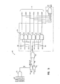
- FIG. 2 One preferred embodiment of the multiple-message unit scrolling means 20 of Fig. 1 is represented by the circuit schematic shown in Fig. 2.
- the message unit address signal is generated by the real time signal means as explained in the discussion of Fig. 1 above in BCD format and appears on the multiple conductor lead 28.
- Each decimal digit of the address number is represented by a four bit combination and is converted to a binary coded signal which is outputted to the multiple conductor line 32 as explained above.
- inverter 102 will remain low until a COMMA signal on line 62 and a character 16 (C16) signal on line 96 occur at the same time thereby keeping the LOAD signal on line 54 low and conditioning the counter 46 to throughput the binary coded message unit address signal upon the occurrence of a clock pulse on lead 56.
- a clock pulse signal is caused to occur when a SELECT MESSAGE signal appears on lead 35 which is fed to one input of an AND gate 108. Since the other input of AND gate 108 is connected to the output of the NOR gate 100 which is held high at this time, the output of gate 108 follows the input SELECT MESSAGE signal.
- the output of gate 108 is connected to one input of a NOR gate 110.
- the output of the NOR gate 110 drives inverter 106 to produce a clock pulse signal on lead 56 to cause the counter 46 output data at terminals DO-D7 and multiple conductor lead 32 to agree with the input message address data on terminals A0-A7 connected to the multiple conductor lead 58.
- a COMMA signal on lead 62 occurs at the same time as a C16 signal on lead 96 and causes the output of AND gate 84 to go high.
- the output of gate 84 is connected to one input of NOR gate 88 and a high signal at the output of gate 84 causes the ouput signal of NOR gate 88 to go low.
- the output signal of gate 88 is inverted by inverter 90, the inverter output being connected via the lead 92 to the input of gate 86 causing the output signal of gate 86 to go high.
- the output of gate 86 is connected to the other input of NOR gate 88 forcing the output signal of inverter 90 to latch high.
- inverter 90 is also connected to one input of a NOR gate 100 forcing the output signal of gate 100 low and the output signal of inverter 102 high.
- the output signal of inverter 102 latches high since its output is fed back on the lead 54 to the other input of the NOR gate 100.
- the counter 46 When the output signal of inverter 102 is high and consequently the LOAD signal on lead 54 is high, the counter 46 is conditioned to count up from the preset binary coded message unit address appearing at the input terminals AO-A7 until the LOAD signal on lead 54 returns to a low state.
- the binary coded message address at the output DO-D7 of counter 46 is incremented each time a clock pulse signal appears on lead 56.
- the message unit clock pulsing circuit 52 comprises a conventional 555 type integrated circuit timer and is enabled when the LOAD signal is high causing the circuit to produce clock pulse signals on a lead 120 connected to an inverter 114.
- the inverted clock pulses from inverter 114 are fed on lead 66 to one input of an AND gate 116, the other input to AND gate 116 being held high by the LOAD signal on lead 54.
- the output of AND gate 116 is connected via the lead 70 to the other input of the clock steering circuit 60 comprising the AND gate 108, NOR gate 110 and inverter 106.
- the output signal of the NOR gate 110 follows the clock pulse signal of the message unit clock pulsing circuit 52 and clocks the counter 46 through inverter 106.
- a new message unit address is produced for each clock pulse generated and the corresponding message unit is selected from memory and displayed in a time-spaced relationship from the previously displayed message unit on the display device 10.
- a PERIOD signal on lead 72 occurs at the same time as a C16 signal on lead 96 and causes the AND gate 94 output signal to go high turning on transistor 98 which connects by the lead 92 the output of inverter 90, the emitter of transistor 104, one input of NOR gate 100 and the input to gate 86 to ground and unlatches the logic loop comprising gates 86, 88 and 90.
- the other input to the NOR gate 100 is forced low when transistor 104 is caused to conduct by the inverter 114 output going high at the next clock pulse.
- the one clock pulse delay is necessary to allow time for the last message unit to be selected from memory and displayed prior to unlatching the logic loop comprising gates 100 and 102.
- the inverter 102 output provides a low LOAD signal on lead 54 disabling counter 46 and resetting the message unit clock pulsing circuit 52.
- the multiple-message unit scrolling circuit 20 is again in a condition to receive a new message unit selection address from the real time means via the multiple conductor lead 28.
- the scrolling speed regulating the display time interval of message units in a multiple-message unit message is controllable over a range of 20 to 60 message units per minute in the preferred embodiment by adjusting variable resistance 122.
- a different desired scrolling speed range may be obtained by selecting the appropriate timing components resistance 122 and capacitor 124 for the message unit clock pulsing circuit 52.
- the reserve digit signal means 18 comprises a reserve digit decoder 74, a reserve digit latch 76 and a reserve character select logic circuit means 78.
- the number of character locations to be reserved is predetermined by the user.
- the message unit may perhaps indicate the rpm of a rotating member at a given location in a mechanism being monitored and the user knows the magnitude of the rpm can always be displayed in the space of three character locations.
- the user inserts a predetermined binary coded signal in the character display signal position immediately preceeding the number of character display locations to be reserved, that is, if character locations 14 through 16 are to be reserved then the predetermined binary coded signal is inserted at character location 13 (C13) in the memory and likewise, if character locations 11 through 16 are to be reserved the predetermined binary coded signal is inserted at character location 10 (C10).
- the reserve digit decoder 74 senses the output from memory 12 on the multiple conductor line 82 which carries the binary coded signals DO-D7 representing the six bit alphanumeric code and the two bit punctuation code.
- the reserve digit decoder generates a LOOK signal on lead 80 in response to sensing the predetermined binary coded signal and activates the reserve digit latch 76.
- a reserve signal is produced on lead 84 when the LOOK signal occurs at the same time that the C10 or C13 signal occurs.
- the predetermined binary coded reserve signal represents an equal sign.
- the reserve digit signal on lead 84 is fed to a reserve character select logic circuit means 78 which generates a RDRT signal on lead 126 to disable the tri-state buffer message latch 34 so that signals representing real time data appearing on the multi-conductor line 28 are not read as message unit address signals but are routed to the tri-state buffer real time data latch 36 to be read as real time data.
- the outputs RC11-RC16 of the reserve character select logic circuit means 78 on the multi-conductor line 44 enable the data latch 36 to transmit the real time BCD data to the memory 12 on the multi- conductor line 38 one character at a time to be decoded by memory 12 for transmission to the display bus 26.
- the enable signals generated by the reserve character select logic circuit means 78 will correspond to the respective character location selected, that is, for example, character location 11 would be selected during the occurence of enable signal RC11.
- FIG. 3 A preferred embodiment of the reserve digit signal means 18 of Fig. 1 is represented by the circuit schematic shown in Fig. 3.
- the binary coded reserve digit signal in the form of a hexi- decimal binary coded signal is transmitted from the memory in the same manner as shown above in Fig. 1 on the multiple conductor lead 82 to an AND gate 74.
- the AND gate 74 When the proper signal levels representing an EQUAL sign are present, the AND gate 74 generates a high signal on lead 80 to enable the reserve digit latch 76.
- character locations 11-16 are reserved as described by the following.
- a high signal is outputted by the digit latch 76 on lead 130 which is connected to one input of each AND gate 132,132 and to one input of an OR gate 134.
- the output of OR gate 134 is connected to one input of each AND gate 136,136.
- the output logic signal of the OR gate 134 is high when the signal on lead 130 is high.
- the AND gates 132, 132, 136, 136 of the reserve character select logic circuit 78 are now conditioned to generate output enable signals RC11-RC16 on the multiple conductor lead 44 when the corresponding character location select signals C11-C16 occur on the multiple conductor lead 130.
- the enable signals RC11-RC16 are also connected to an OR circuit means 138 to generate the RDRT signal on lead 126 whenever any one of the RC11-RC16 signals are high.
- character locations 14-16 are reserved when a C13 signal occurs on lead 140 at the same time that the EQUAL sign signal occurs on lead 80 causing digit latch 76 to output a high signal on lead 142 which is connected to the other input of OR gate 134.
- the AND gates 136,136 are conditioned to generate the output enable logic signals on RC14-RC16 when the corresponding character location select logic signals C14-C16 occur.
- the OR circuit means 138 will produce an RDRT signal on lead 126 whenever any one of the RC14-RC16 signals are high.
- the character location logic signals C1-C16 on the multiple conductor lead 130 are generated by the master clock means 16 of Fig. 1.
Landscapes
- Engineering & Computer Science (AREA)
- Theoretical Computer Science (AREA)
- Physics & Mathematics (AREA)
- General Physics & Mathematics (AREA)
- Computer Hardware Design (AREA)
- Human Computer Interaction (AREA)
- General Engineering & Computer Science (AREA)
- Control Of Indicators Other Than Cathode Ray Tubes (AREA)
- Controls And Circuits For Display Device (AREA)
- Selective Calling Equipment (AREA)
- Financial Or Insurance-Related Operations Such As Payment And Settlement (AREA)
Abstract
Description
- This invention relates to a system for displaying alphanumeric messages by means of a unitary visual display device and deals more particularly with apparatus for expanding the message display capacity of such a device.
- Multiple character station unitary visual display devices used in display systems are generally well known in the art. Such multiple character display devices generally have a fixed number of character stations which limit the number of characters in the displayed message to the number of character display stations of the device. One such display system employing a limited capacity multiple character station device is illustrated and described in U.S. Patent No. 4,381,505 assigned to the assignee of the present invention.
- Although the aforementioned display system has numerous applications, it is often found in industrial applications utilizing an automatic controller or monitoring. device for a manufacturing, material handling, chemical or other industrial process. In such uses the controller may operate to select a message unit from a memory in accordance with different conditions monitored by the controller which when displayed advises an operator of a monitored condition, provides a warning, gives an instruction or the like, or the controller may also select a stored message component from the memory to which is added real time data representing the value of real time variables or other associated real time conditions.
- Often it is necessary to display a message unit exceeding the number of character stations of the display device or to display a sequence of message units to provide additional information or instructions to an operator. A limitation in displaying multiple-message unit messages in a unitary visual display device system is generally the expense and complexity associated with the additional equipment such as memory modules and software programming in the controller operating with such a display system.
- Another drawback often associated with the above described display systems is the additional equipment required in the controller to convert binary coded decimal (BCD) signals representative of a message unit address to binary coded signals to select messages from the display system memory. Since the real time data is represented in BCD signal format, separate multiconductor lines for message selection signals and real time data signals are required to connect the associated controller outputs to separate BCD and binary input ports in the display system.
- Still another limitation is the additional controller equipment and associated software required to provide a reserve signal to the display system to reserve character locations in the visual display device to display real time data associated with a stored message component having a real time message component.
- Accordingly, it is desirable to have a unitary visual display system for use with controllers or the like capable of displaying multiple-message unit messages wherein the message units may be made up of entirely stored message units or message units having both stored and real time components and that avoids the drawbacks of the aforedescribed display systems.
- The general aim of the present invention is to provide an improved alphanumeric unitary visual display system having an expanded message display capability that overcomes the limitations of previously used unitary visual display systems. The unitary visual display system of the present invention provides multiple-message unit message display capability and real time data reserve signals without the complex hardware, software, and wiring generally required in controllers used with prior display systems.
- Other objects and advantages of the invention will be apparent from the following written detailed description and from the accompanying drawings.
- The invention resides in a circuit for scrolling message units in an alphanumeric visual display system having a unitary multi-character station limited capacity character display device. The message units are stored in a memory means and are made up of a plurality of characters not greater in number than the number of character stations of the display device and each message unit has a predetermined character display signal position. Some of the message units are comprised of stored message components and real time message components with the stored message components having a plurality of characters smaller in number than the number of character stations of the display device. A real time signal means associated with a plurality of real time conditions provides a selection of real time message components. A complete message comprises a single message unit or a number of message units in sequence.
- The invention more specifically resides in a first signal means to indicate the first message unit in a complete message and a first sensing means to detect the presence of the first signal means in a first predetermined character display signal position. A scrolling activation circuit means is responsive to the detection of the first signal means and enables a message unit scrolling means circuit so that each message unit of a complete message is automatically accessed and selected from the memory means and displayed in a time-spaced relationship by the visual display device.
- The invention further resides in a second signal means to indicate the last message unit in a complete message and a second sensing means to detect the presence of the second signal means in a second predetermined character display signal position to deactivate the scrolling circuit means.
- The invention also resides in a reserve digit signal means to indicate that a message unit includes a stored message component and a real time message component. A third sensing means detects the presence of the reserve digit signal means in a third predetermined character display signal position. A reserve character select logic circuit means responsive to the third sensing means reserves a number of character display locations of the visual display device to display in the reserved locations a corresponding number of characters comprising the real time message component.
-
- Fig. 1 shows in block diagram form an alphanumeric display system embodying the present invention,
- Fig. 2 shows partly in schematic form and partly in block diagram form the multiple-message unit scrolling means circuit of Fig. 1, and
- Fig. 3 shows in schematic form the reserve digit real time signal means circuit of Fig. 1.
- A representative system for displaying alphanumeric messages by means of a multi-character station unitary visual display device having a limited capacity character display and capable of embodying the present invention is manufactured by The Arthur G. Russell Company, Incorporated, of Bristol, Connecticut. Briefly, the system has a display device with a row of character stations at each of which a character may be created for display in response to a set of signals applied to the character station. A memory device stores a plurality of message units, some of which are complete message units and others of which are stored message components. The message units selected by a real time means are converted by a control circuit into a set of signals which are applied in a one to one relationship to the character stations of the display device to cause the display of a single complete message unit. The display system is illustrated and described in U.S. Patent No. 4,381,505, issued April 26, 1983 and assigned to the assignee of the present invention.
- Turning now to the invention of the present disclosure, Fig. 1 shows in block diagram form, an alphanumeric unitary visual display system designated generally by the numeral 8 embodying the invention. The display system comprises a multi-character station unitary
visual display device 10, a memory means 12 which stores a variety of message units, a real time signal means shown generally at 14 providing a selection of real time message components, a master clock means 16, a reserve digit real time signal means 18 for reserving a plurality of character stations to display a real time message component and a multiple-message unit scrolling means 20. - The memory means 12 may take various forms such as a programmable-read-only-memory (PROM) or an eraseable- programmable-read-only-memory (EPROM) and stores a number of message units each assigned a number of character storage locations in the memory equal in number to the number of character display stations of the
display device 10 which in the preferred embodiment is 16. A stored message unit as described below is selected frommemory 12 by a binary coded message address signal applied to the address terminals A4-A10 via a multipleconductor address line 22. The individual character locations of a selected message unit are in turn selected by a character address signal supplied by a four conductorcharacter address line 24 connected to four corresponding address terminals A0-A3 of thememory 12. The information stored at the character location so selected is read out ofmemory 12 in the form of a nineteen bit binary coded signal onto acharacter bus 26. - A more detailed explanation of the display device and alphanumeric character signal generation may be had by referring to the aforementioned U.S. patent which is hereby adopted by reference into the present disclosure.
- A complete message as used in this disclosure is one made up of one or a plurality of complete message units. A complete message unit may be entirely stored in memory or may be made up of a stored message component and a real time message component provided by a real time signal means. When the complete message unit is entirely stored in memory, display information is contained at all sixteen of their character locations in the
memory 12. When the complete message unit includes a stored message component, display information is contained at less than all of their sixteen character locations in memory. The length of a stored message component may vary in different embodiments but in the embodiment of Fig. 1 it may be either thirteen characters long or ten characters long. More specifically, for each stored message component either three or six of the display stations of thedisplay 10 may be reserved for the character display of real time information and when such stations are reserved, no meaningful information is stored in the corresponding character locations of the memory. Such reservation is indicated by a predetermined coded reserve signal and is explained in further detail below. - The real time signal means 14 functions to select the message to be displayed by the
display device 10. This is done by outputting a message unit address signal on themultiple conductor line 28 connecting the real time signal means 14 to the scrolling means 20 of the display system 8. The message address signal is in turn outputted from the scrolling means 20 on the multiple conductor line 32 to a tri-statebuffer message latch 34. The selected message unit address signal is outputted onto themessage address line 22 to access a complete stored message unit or a stored message component in thememory 12 when thelatch 34 is enabled by a message select signal on line 35. - When the real time signal means 14 selects a stored message component that requires real time information to form a complete message unit, a read real time (RDRT) signal disables the tri-state
message latch 34 so that real time data appearing on themultiple conductor line 28 is fed to a tri-state buffer real time data latch 36. This real time data is transferred to address terminals A0-A3 of the memory 12 by means of amultiple conductor line 38. Real time data appearing in character locations 14-16 and 11-13 is transferred to thememory 12 and in turn to thecharacter bus 26 one character location at a time as the corresponding select digit signal onlines buffer 36 when a corresponding reserve character select enable signal RC11-RC16 is present on themultiple conductor lead 44. - To display a complete message made up of multiple message units, the message units stored in the
memory 12 include at least one wherein a first predetermined binary coded signal occurs at a first predetermined character display signal location in memory indicating the end of the first message unit in a plurality of message units and that the immediately succeeding message address locations in memory contain the message units necessary to form the complete message. The end of the first message unit signal activates the scrolling means 20 to generate the required message address signals to select the succeeding message units from thememory 12 to be displayed by the visual display device. Additionally, the message units stored in thememory 12 comprising a multiple-message unit message include at least one message unit wherein a second predetermined binary coded signal occurs at a second predetermined character display signal location in memory of the last message unit in a multiple-message unit message to indicate the end of a complete message. The end of complete message signal disables the scrolling means 20 and permits a new message to be selected. In the preferred embodiment, the first and second predetermined binary coded signal representations are preferably displayed in the last character display location of thedisplay device 10 and represent a comma and a period respectively. However, it is not necessary that the signals occur in a character display location but may be in a non-display location in memory associated with the respective multiple-message unit, for example, perhaps a seventeenth memory location. - Considering now in further detail the multiple message unit scrolling means 20 of Fig. 1. The scrolling means 20 comprises a BCD to
binary decoder 30, a message unit address means 46, a multiple-message unit/end of message sensing circuit means 48, a scrolling activation means 50, a clock steering logic circuit means 60 and a message unit clock pulsing means 52. Message unit address signals in the form of BCD data are carried on themultiple conductor line 28 from the real time signal means 14 to the corresponding mesasge unit selection means or BCD tobinary decoder 30 input terminals. Since thememory 12 requires a binary coded signal to access a memory location, the BCD formated message unit address signal is converted by the BCD tobinary decoder 30 to a binary coded signal representative of the message unit address and is loaded into the message unit address means or asynchronous programmablebinary counter 46 by means of amultiple conductor line 58. When the LOAD signal is present onlead 54 the counter is preset, that is, the output of thecounter 46 will agree with the message unit address signal data present on theinput line 58 upon the occurence of a clock pulse signal onlead 56. The necessary clock pulse signal is generated by the clock steering logic circuit means 60 when a SELECT MESSAGE signal is generated on line 35 by the real time signal means 14. - When the message unit selected from the
memory 12 is one that is part of a multiple-message unit message, a COMMA signal present onlead 62 indicates that during the time of the sixteenth character location in the message unit the binary coded signal representative of a comma has been decoded. The sensing circuit means 48 is also activated during the time that the sixteenth character is displayed and in response to the detection of the COMMA signal produces an ENABLE signal onlead 64. The multiple-message unit logic circuit means 50 in response to the ENABLE signal generates a START multiple-message unit signal onlead 66 causing the message unitclock pulsing circuit 52 to produce clock pulse signals onlead 68 at a desired preset frequency. The clock pulse signals are fed to theclock steering circuit 60 which directs the clock pulse signals to thecounter 46 onlead 56. The scrolling activation means 50 also produces during the time of a multiple-message unit message a signal on theLOAD lead 54 to enable thecounter 46 to count up sequentially from the selected message unit address value that was loaded into thecounter 46 to generate each next succeeding message address signal to select the corresponding next message unit of the multiple-message unit message from thememory 12. When the final message unit of a multiple-message unit message is displayed, a PERIOD signal present onlead 72 indicates that during the time of the sixteenth character location in the message unit a binary coded signal representative of a period has been decoded. The sensing circuit means 48 is activated during the time that the sixteenth character is displayed and in response to the detection of the PERIOD signal produces an END signal onlead 64. The scrolling activation means 50-in response to the END signal sends a STOP signal onlead 66 to the message unitclock pulsing circuit 52 to deactivate the clock circuit. The scrolling activation means 50 also generates a LOAD signal onlead 54 to disable thecounter 46. - One preferred embodiment of the multiple-message unit scrolling means 20 of Fig. 1 is represented by the circuit schematic shown in Fig. 2. Referring now to Fig. 2, the message unit address signal is generated by the real time signal means as explained in the discussion of Fig. 1 above in BCD format and appears on the
multiple conductor lead 28. Each decimal digit of the address number is represented by a four bit combination and is converted to a binary coded signal which is outputted to themultiple conductor line 32 as explained above. By inspection it can be seen that the output ofinverter 102 will remain low until a COMMA signal online 62 and a character 16 (C16) signal online 96 occur at the same time thereby keeping the LOAD signal online 54 low and conditioning thecounter 46 to throughput the binary coded message unit address signal upon the occurrence of a clock pulse onlead 56. A clock pulse signal is caused to occur when a SELECT MESSAGE signal appears on lead 35 which is fed to one input of an ANDgate 108. Since the other input of ANDgate 108 is connected to the output of the NORgate 100 which is held high at this time, the output ofgate 108 follows the input SELECT MESSAGE signal. The output ofgate 108 is connected to one input of a NORgate 110. The output of the NORgate 110 drivesinverter 106 to produce a clock pulse signal onlead 56 to cause thecounter 46 output data at terminals DO-D7 andmultiple conductor lead 32 to agree with the input message address data on terminals A0-A7 connected to themultiple conductor lead 58. - .. When the message unit address selected is a mul- tiple/message unit message, a COMMA signal on
lead 62 occurs at the same time as a C16 signal onlead 96 and causes the output of ANDgate 84 to go high. The output ofgate 84 is connected to one input of NORgate 88 and a high signal at the output ofgate 84 causes the ouput signal of NORgate 88 to go low. The output signal ofgate 88 is inverted byinverter 90, the inverter output being connected via thelead 92 to the input ofgate 86 causing the output signal ofgate 86 to go high. The output ofgate 86 is connected to the other input of NORgate 88 forcing the output signal ofinverter 90 to latch high. The output ofinverter 90 is also connected to one input of a NORgate 100 forcing the output signal ofgate 100 low and the output signal ofinverter 102 high. The output signal ofinverter 102 latches high since its output is fed back on thelead 54 to the other input of the NORgate 100. - When the output signal of
inverter 102 is high and consequently the LOAD signal onlead 54 is high, thecounter 46 is conditioned to count up from the preset binary coded message unit address appearing at the input terminals AO-A7 until the LOAD signal onlead 54 returns to a low state. The binary coded message address at the output DO-D7 ofcounter 46 is incremented each time a clock pulse signal appears onlead 56. The message unitclock pulsing circuit 52 comprises a conventional 555 type integrated circuit timer and is enabled when the LOAD signal is high causing the circuit to produce clock pulse signals on a lead 120 connected to aninverter 114. The inverted clock pulses frominverter 114 are fed onlead 66 to one input of an ANDgate 116, the other input to ANDgate 116 being held high by the LOAD signal onlead 54. The output of ANDgate 116 is connected via thelead 70 to the other input of theclock steering circuit 60 comprising the ANDgate 108, NORgate 110 andinverter 106. The output signal of the NORgate 110 follows the clock pulse signal of the message unitclock pulsing circuit 52 and clocks thecounter 46 throughinverter 106. A new message unit address is produced for each clock pulse generated and the corresponding message unit is selected from memory and displayed in a time-spaced relationship from the previously displayed message unit on thedisplay device 10. When the last message unit in a multiple-message unit message is displayed, a PERIOD signal onlead 72 occurs at the same time as a C16 signal onlead 96 and causes the ANDgate 94 output signal to go high turning ontransistor 98 which connects by thelead 92 the output ofinverter 90, the emitter oftransistor 104, one input of NORgate 100 and the input togate 86 to ground and unlatches the logicloop comprising gates gate 100 is forced low whentransistor 104 is caused to conduct by theinverter 114 output going high at the next clock pulse. The one clock pulse delay is necessary to allow time for the last message unit to be selected from memory and displayed prior to unlatching the logicloop comprising gates inverter 102 output provides a low LOAD signal onlead 54 disablingcounter 46 and resetting the message unitclock pulsing circuit 52. The multiple-messageunit scrolling circuit 20 is again in a condition to receive a new message unit selection address from the real time means via themultiple conductor lead 28. - The scrolling speed regulating the display time interval of message units in a multiple-message unit message is controllable over a range of 20 to 60 message units per minute in the preferred embodiment by adjusting
variable resistance 122. A different desired scrolling speed range may be obtained by selecting the appropriatetiming components resistance 122 andcapacitor 124 for the message unitclock pulsing circuit 52. - Considering now in further detail the reserve digit real time signal means 18 of Fig. 1. The reserve digit signal means 18 comprises a
reserve digit decoder 74, areserve digit latch 76 and a reserve character select logic circuit means 78. As stated above, to display real time data when the selected message unit is one having a stored message component and a real time message component, it is necessary to reserve either three or six digits in accordance with the number of character display locations required to display the real time data. The number of character locations to be reserved is predetermined by the user. For example, the message unit may perhaps indicate the rpm of a rotating member at a given location in a mechanism being monitored and the user knows the magnitude of the rpm can always be displayed in the space of three character locations. Consequently only three character locations need be reserved. Therefore, when the characters comprising the message unit are coded for storage in the character locations in memory, the user inserts a predetermined binary coded signal in the character display signal position immediately preceeding the number of character display locations to be reserved, that is, ifcharacter locations 14 through 16 are to be reserved then the predetermined binary coded signal is inserted at character location 13 (C13) in the memory and likewise, if character locations 11 through 16 are to be reserved the predetermined binary coded signal is inserted at character location 10 (C10). Thereserve digit decoder 74 senses the output frommemory 12 on themultiple conductor line 82 which carries the binary coded signals DO-D7 representing the six bit alphanumeric code and the two bit punctuation code. The reserve digit decoder generates a LOOK signal on lead 80 in response to sensing the predetermined binary coded signal and activates thereserve digit latch 76. A reserve signal is produced onlead 84 when the LOOK signal occurs at the same time that the C10 or C13 signal occurs. In the preferred embodiment, the predetermined binary coded reserve signal represents an equal sign. The reserve digit signal onlead 84 is fed to a reserve character select logic circuit means 78 which generates a RDRT signal onlead 126 to disable the tri-state buffer message latch 34 so that signals representing real time data appearing on themulti-conductor line 28 are not read as message unit address signals but are routed to the tri-state buffer real time data latch 36 to be read as real time data. The outputs RC11-RC16 of the reserve character select logic circuit means 78 on themulti-conductor line 44 enable the data latch 36 to transmit the real time BCD data to thememory 12 on the multi-conductor line 38 one character at a time to be decoded bymemory 12 for transmission to thedisplay bus 26. It will be understood that the enable signals generated by the reserve character select logic circuit means 78 will correspond to the respective character location selected, that is, for example, character location 11 would be selected during the occurence of enable signal RC11. - A preferred embodiment of the reserve digit signal means 18 of Fig. 1 is represented by the circuit schematic shown in Fig. 3. Referring now to Fig. 3, the binary coded reserve digit signal in the form of a hexi- decimal binary coded signal is transmitted from the memory in the same manner as shown above in Fig. 1 on the
multiple conductor lead 82 to an ANDgate 74. When the proper signal levels representing an EQUAL sign are present, the ANDgate 74 generates a high signal onlead 80 to enable thereserve digit latch 76. When a C10 signal occurs onlead 128 at the same time that the EQUAL sign signal occurs, character locations 11-16 are reserved as described by the following. A high signal is outputted by thedigit latch 76 onlead 130 which is connected to one input of each AND gate 132,132 and to one input of anOR gate 134. The output of ORgate 134 is connected to one input of each AND gate 136,136. The output logic signal of theOR gate 134 is high when the signal onlead 130 is high. The ANDgates select logic circuit 78 are now conditioned to generate output enable signals RC11-RC16 on themultiple conductor lead 44 when the corresponding character location select signals C11-C16 occur on themultiple conductor lead 130. The enable signals RC11-RC16 are also connected to an OR circuit means 138 to generate the RDRT signal onlead 126 whenever any one of the RC11-RC16 signals are high. In a similar manner, character locations 14-16 are reserved when a C13 signal occurs onlead 140 at the same time that the EQUAL sign signal occurs onlead 80 causingdigit latch 76 to output a high signal onlead 142 which is connected to the other input of ORgate 134. In this instance only the AND gates 136,136 are conditioned to generate the output enable logic signals on RC14-RC16 when the corresponding character location select logic signals C14-C16 occur. The OR circuit means 138 will produce an RDRT signal onlead 126 whenever any one of the RC14-RC16 signals are high. - The character location logic signals C1-C16 on the
multiple conductor lead 130 are generated by the master clock means 16 of Fig. 1. - Apparatus for expanding the display capacity of an alphanumeric unitary visual display system having a limited number of character display locations by scrolling a plurality of message units to form multiple-message unit messages has been described in a preferred embodiment and numerous substitutions and modifications can be had without departing from the spirit of the invention. Accordingly, the present invention has been described merely by way of illustration rather than limitation.
Claims (16)
Priority Applications (1)
| Application Number | Priority Date | Filing Date | Title |
|---|---|---|---|
| AT84304457T ATE51314T1 (en) | 1983-08-05 | 1984-06-29 | DISPLAY SYSTEM FOR ALPHANUMERIC MESSAGES. |
Applications Claiming Priority (2)
| Application Number | Priority Date | Filing Date | Title |
|---|---|---|---|
| US520630 | 1983-08-05 | ||
| US06/520,630 US4660031A (en) | 1983-08-05 | 1983-08-05 | System for displaying alphanumeric messages |
Publications (3)
| Publication Number | Publication Date |
|---|---|
| EP0133344A2 true EP0133344A2 (en) | 1985-02-20 |
| EP0133344A3 EP0133344A3 (en) | 1986-12-17 |
| EP0133344B1 EP0133344B1 (en) | 1990-03-21 |
Family
ID=24073423
Family Applications (1)
| Application Number | Title | Priority Date | Filing Date |
|---|---|---|---|
| EP84304457A Expired - Lifetime EP0133344B1 (en) | 1983-08-05 | 1984-06-29 | System for displaying alphanumeric messages |
Country Status (6)
| Country | Link |
|---|---|
| US (1) | US4660031A (en) |
| EP (1) | EP0133344B1 (en) |
| JP (1) | JPS60100185A (en) |
| AT (1) | ATE51314T1 (en) |
| CA (1) | CA1233280A (en) |
| DE (1) | DE3481740D1 (en) |
Cited By (8)
| Publication number | Priority date | Publication date | Assignee | Title |
|---|---|---|---|---|
| GB2182473A (en) * | 1985-10-30 | 1987-05-13 | Mitsubishi Electric Corp | Display control apparatus for elevator |
| FR2611953A1 (en) * | 1987-02-27 | 1988-09-09 | Smh Alcatel | ELECTRONIC DISPLAY MACHINE WITH SELECTION OF OPERATING MODE |
| FR2611947A1 (en) * | 1987-02-27 | 1988-09-09 | Smh Alcatel | POSTING MACHINE COMPRISING AN ALARM |
| FR2611946A1 (en) * | 1987-02-27 | 1988-09-09 | Smh Alcatel | ELECTRONIC AFFRANCHING MACHINE HAVING VALUES LIMITING POSTAGE |
| EP0281862A1 (en) * | 1987-02-27 | 1988-09-14 | Neopost Industrie | Operation system for an electronic postage meter |
| GB2219678A (en) * | 1985-10-30 | 1989-12-13 | Mitsubishi Electric Corp | Elevator display control |
| GB2225886A (en) * | 1988-11-10 | 1990-06-13 | Fmc Corp | Programmable message display |
| DE102015122811A1 (en) * | 2015-12-23 | 2017-06-29 | Balluff Gmbh | Display device and method for driving a display device |
Families Citing this family (6)
| Publication number | Priority date | Publication date | Assignee | Title |
|---|---|---|---|---|
| KR900006931B1 (en) * | 1986-02-25 | 1990-09-25 | 미쓰비시전기 주식회사 | Devices displaying of elevators signal |
| US4837807A (en) * | 1987-12-30 | 1989-06-06 | American Telephone And Telegraph Company | Station to station message arrangement |
| US5187797A (en) * | 1988-09-28 | 1993-02-16 | Solatrol, Inc. | Machine interface system with hierarchal menus allowing user sequencing and selection of menu items by actuation of three switches |
| US5194702A (en) * | 1991-09-17 | 1993-03-16 | Swonger Jr Karl W | Vertically scrolled elevator position indicator |
| CA2273734A1 (en) * | 1998-07-08 | 2000-01-08 | Robert D. Ross | Vending machine display |
| US8107599B2 (en) * | 2005-02-15 | 2012-01-31 | Fastvdo, Llc | Methods and apparatus for the composition and communication of digital composition coded multisensory messages (DCC MSMS) |
Citations (2)
| Publication number | Priority date | Publication date | Assignee | Title |
|---|---|---|---|---|
| US4359730A (en) * | 1979-10-30 | 1982-11-16 | Sharp Kabushiki Kaisha | Alphanumeric display controlled by microprocessor |
| US4381505A (en) * | 1980-12-10 | 1983-04-26 | The Arthur G. Russell Company, Incorporated | System for displaying alphanumerical messages having stored and real time components |
Family Cites Families (8)
| Publication number | Priority date | Publication date | Assignee | Title |
|---|---|---|---|---|
| US3868675A (en) * | 1973-09-04 | 1975-02-25 | Capsule Communications Inc | Display system with combined dynamic and static display |
| JPS5525679B2 (en) * | 1974-08-01 | 1980-07-08 | ||
| US4373192A (en) * | 1979-08-27 | 1983-02-08 | Sharp Kabushiki Kaisha | Display device of an electronic language interpreter |
| IT1143292B (en) * | 1981-01-22 | 1986-10-22 | Olivetti & Co Spa | DISPLAY DEVICE FOR COPIERS |
| US4467323A (en) * | 1981-12-04 | 1984-08-21 | Bear Automotive Service Equipment Company | Engine analyzer with simulated analog meter display |
| JPS58212972A (en) * | 1982-06-04 | 1983-12-10 | Sharp Corp | Memorandum printing device |
| JPH0675220B2 (en) * | 1982-10-12 | 1994-09-21 | 富士ゼロックス株式会社 | Text display |
| JP3238884B2 (en) * | 1997-06-17 | 2001-12-17 | 丸誠重工業株式会社 | Intermediate girder mounting device for bar screen for dust remover |
-
1983
- 1983-08-05 US US06/520,630 patent/US4660031A/en not_active Expired - Fee Related
-
1984
- 1984-06-29 EP EP84304457A patent/EP0133344B1/en not_active Expired - Lifetime
- 1984-06-29 DE DE8484304457T patent/DE3481740D1/en not_active Expired - Lifetime
- 1984-06-29 CA CA000457850A patent/CA1233280A/en not_active Expired
- 1984-06-29 AT AT84304457T patent/ATE51314T1/en not_active IP Right Cessation
- 1984-07-31 JP JP59161474A patent/JPS60100185A/en active Pending
Patent Citations (2)
| Publication number | Priority date | Publication date | Assignee | Title |
|---|---|---|---|---|
| US4359730A (en) * | 1979-10-30 | 1982-11-16 | Sharp Kabushiki Kaisha | Alphanumeric display controlled by microprocessor |
| US4381505A (en) * | 1980-12-10 | 1983-04-26 | The Arthur G. Russell Company, Incorporated | System for displaying alphanumerical messages having stored and real time components |
Cited By (20)
| Publication number | Priority date | Publication date | Assignee | Title |
|---|---|---|---|---|
| GB2219677B (en) * | 1985-10-30 | 1990-05-16 | Mitsubishi Electric Corp | Display control apparatus for elevator |
| GB2219677A (en) * | 1985-10-30 | 1989-12-13 | Mitsubishi Electric Corp | Elevator display control |
| GB2219678A (en) * | 1985-10-30 | 1989-12-13 | Mitsubishi Electric Corp | Elevator display control |
| GB2182473A (en) * | 1985-10-30 | 1987-05-13 | Mitsubishi Electric Corp | Display control apparatus for elevator |
| GB2219678B (en) * | 1985-10-30 | 1990-05-02 | Mitsubishi Electric Corp | Display control apparatus for elevator |
| GB2182473B (en) * | 1985-10-30 | 1990-05-02 | Mitsubishi Electric Corp | Display control apparatus for elevator |
| EP0281861A1 (en) * | 1987-02-27 | 1988-09-14 | Neopost Industrie | Electronic postage meter comprising postage-limiting values |
| FR2611953A1 (en) * | 1987-02-27 | 1988-09-09 | Smh Alcatel | ELECTRONIC DISPLAY MACHINE WITH SELECTION OF OPERATING MODE |
| FR2617313A1 (en) * | 1987-02-27 | 1988-12-30 | Smh Alcatel | SYSTEM FOR OPERATING AN ELECTRONIC AFFRANCHING MACHINE |
| US4928249A (en) * | 1987-02-27 | 1990-05-22 | Societe Anonyme Dite : Smh Alcatel | Operating system for an electronic franking machine |
| EP0284779A1 (en) * | 1987-02-27 | 1988-10-05 | Alcatel Satmam | Postage meter comprising an alarm |
| US4905156A (en) * | 1987-02-27 | 1990-02-27 | Societe Anonyme Dite : Smh Alcatel | Franking machine including an alarm |
| US4918601A (en) * | 1987-02-27 | 1990-04-17 | Smh Alcatel | Electronic franking machine with operating mode selection |
| EP0281862A1 (en) * | 1987-02-27 | 1988-09-14 | Neopost Industrie | Operation system for an electronic postage meter |
| EP0281860A1 (en) * | 1987-02-27 | 1988-09-14 | Alcatel Satmam | Electronic postage meter with a working mode selection |
| FR2611946A1 (en) * | 1987-02-27 | 1988-09-09 | Smh Alcatel | ELECTRONIC AFFRANCHING MACHINE HAVING VALUES LIMITING POSTAGE |
| US4928244A (en) * | 1987-02-27 | 1990-05-22 | Societe Anonyme Dite : Smh Alcatel | Electronic franking machine including franking limit values |
| FR2611947A1 (en) * | 1987-02-27 | 1988-09-09 | Smh Alcatel | POSTING MACHINE COMPRISING AN ALARM |
| GB2225886A (en) * | 1988-11-10 | 1990-06-13 | Fmc Corp | Programmable message display |
| DE102015122811A1 (en) * | 2015-12-23 | 2017-06-29 | Balluff Gmbh | Display device and method for driving a display device |
Also Published As
| Publication number | Publication date |
|---|---|
| EP0133344A3 (en) | 1986-12-17 |
| DE3481740D1 (en) | 1990-04-26 |
| ATE51314T1 (en) | 1990-04-15 |
| CA1233280A (en) | 1988-02-23 |
| EP0133344B1 (en) | 1990-03-21 |
| US4660031A (en) | 1987-04-21 |
| JPS60100185A (en) | 1985-06-04 |
Similar Documents
| Publication | Publication Date | Title |
|---|---|---|
| US4660031A (en) | System for displaying alphanumeric messages | |
| US3818461A (en) | Buffer memory system | |
| US3470542A (en) | Modular system design | |
| US3921148A (en) | Business machine communication system and data display | |
| US4064395A (en) | Machine control system employing a programmable machine function controller | |
| US4870571A (en) | Intercomputer communications based on message broadcasting with receiver selection | |
| US4200936A (en) | Asynchronous bidirectional direct serial interface linking a programmable machine function controller and a numerical control | |
| US4065810A (en) | Data transfer system | |
| US4117469A (en) | Computer assisted display processor having memory sharing by the computer and the processor | |
| US5319783A (en) | Programmable controller with an operator messaging function | |
| US4142246A (en) | Sequence controller with dynamically changeable program | |
| US4017831A (en) | N/C machine paging, status and report system | |
| US4525804A (en) | Interface apparatus for host computer and graphics terminal | |
| US3952289A (en) | Controller for linking a typewriter console to a processor unit | |
| US4130883A (en) | Data communication system having bidirectional station interfaces | |
| US3761882A (en) | Process control computer | |
| US3651481A (en) | Readout system for visually displaying stored data | |
| US4326263A (en) | Method and apparatus for controlling a plurality of like equipments | |
| US3958225A (en) | Apparatus and method for controlling a communications terminal | |
| US3760169A (en) | Interface system for direct numeric control of automatic wiring machines | |
| US4959773A (en) | Adapter for attaching I/O devices to I/O communications with alternating read and write modes link | |
| EP0145530A2 (en) | Arrangement for providing data signals for a data display system | |
| US3970989A (en) | Data transfer error check | |
| EP0273749B1 (en) | Display system with fewer display memory chips | |
| JPH01116706A (en) | Picture displaying method for display device of controller |
Legal Events
| Date | Code | Title | Description |
|---|---|---|---|
| PUAI | Public reference made under article 153(3) epc to a published international application that has entered the european phase |
Free format text: ORIGINAL CODE: 0009012 |
|
| AK | Designated contracting states |
Designated state(s): AT BE CH DE FR GB IT LI LU NL SE |
|
| PUAL | Search report despatched |
Free format text: ORIGINAL CODE: 0009013 |
|
| AK | Designated contracting states |
Kind code of ref document: A3 Designated state(s): AT BE CH DE FR GB IT LI LU NL SE |
|
| 17P | Request for examination filed |
Effective date: 19861216 |
|
| 17Q | First examination report despatched |
Effective date: 19890217 |
|
| GRAA | (expected) grant |
Free format text: ORIGINAL CODE: 0009210 |
|
| AK | Designated contracting states |
Kind code of ref document: B1 Designated state(s): AT BE CH DE FR GB IT LI LU NL SE |
|
| PG25 | Lapsed in a contracting state [announced via postgrant information from national office to epo] |
Ref country code: NL Effective date: 19900321 Ref country code: IT Free format text: LAPSE BECAUSE OF FAILURE TO SUBMIT A TRANSLATION OF THE DESCRIPTION OR TO PAY THE FEE WITHIN THE PRESCRIBED TIME-LIMIT;WARNING: LAPSES OF ITALIAN PATENTS WITH EFFECTIVE DATE BEFORE 2007 MAY HAVE OCCURRED AT ANY TIME BEFORE 2007. THE CORRECT EFFECTIVE DATE MAY BE DIFFERENT FROM THE ONE RECORDED. Effective date: 19900321 Ref country code: BE Effective date: 19900321 Ref country code: AT Effective date: 19900321 |
|
| REF | Corresponds to: |
Ref document number: 51314 Country of ref document: AT Date of ref document: 19900415 Kind code of ref document: T |
|
| REF | Corresponds to: |
Ref document number: 3481740 Country of ref document: DE Date of ref document: 19900426 |
|
| ET | Fr: translation filed | ||
| PGFP | Annual fee paid to national office [announced via postgrant information from national office to epo] |
Ref country code: FR Payment date: 19900613 Year of fee payment: 7 |
|
| PGFP | Annual fee paid to national office [announced via postgrant information from national office to epo] |
Ref country code: SE Payment date: 19900615 Year of fee payment: 7 Ref country code: GB Payment date: 19900615 Year of fee payment: 7 |
|
| REG | Reference to a national code |
Ref country code: CH Ref legal event code: PL |
|
| PG25 | Lapsed in a contracting state [announced via postgrant information from national office to epo] |
Ref country code: LU Free format text: LAPSE BECAUSE OF NON-PAYMENT OF DUE FEES Effective date: 19900630 Ref country code: LI Free format text: LAPSE BECAUSE OF NON-PAYMENT OF DUE FEES Effective date: 19900630 Ref country code: CH Free format text: LAPSE BECAUSE OF NON-PAYMENT OF DUE FEES Effective date: 19900630 |
|
| PGFP | Annual fee paid to national office [announced via postgrant information from national office to epo] |
Ref country code: DE Payment date: 19900731 Year of fee payment: 7 |
|
| NLV1 | Nl: lapsed or annulled due to failure to fulfill the requirements of art. 29p and 29m of the patents act | ||
| PLBE | No opposition filed within time limit |
Free format text: ORIGINAL CODE: 0009261 |
|
| PLBI | Opposition filed |
Free format text: ORIGINAL CODE: 0009260 |
|
| 26 | Opposition filed |
Opponent name: GRUNDIG E.M.V. ELEKTRO-MECHANISCHE VERSUCHSANSTALT Effective date: 19901219 |
|
| 26N | No opposition filed | ||
| PG25 | Lapsed in a contracting state [announced via postgrant information from national office to epo] |
Ref country code: GB Effective date: 19910629 |
|
| PG25 | Lapsed in a contracting state [announced via postgrant information from national office to epo] |
Ref country code: SE Effective date: 19910630 |
|
| GBPC | Gb: european patent ceased through non-payment of renewal fee | ||
| PG25 | Lapsed in a contracting state [announced via postgrant information from national office to epo] |
Ref country code: FR Effective date: 19920228 |
|
| PG25 | Lapsed in a contracting state [announced via postgrant information from national office to epo] |
Ref country code: DE Effective date: 19920401 |
|
| REG | Reference to a national code |
Ref country code: FR Ref legal event code: ST |
|
| EUG | Se: european patent has lapsed |
Ref document number: 84304457.9 Effective date: 19920109 |
|
| RDAG | Patent revoked |
Free format text: ORIGINAL CODE: 0009271 |
|
| STAA | Information on the status of an ep patent application or granted ep patent |
Free format text: STATUS: PATENT REVOKED |
|
| 27W | Patent revoked |
Effective date: 19950601 |
|
| REG | Reference to a national code |
Ref country code: CH Ref legal event code: PL |
|
| APAH | Appeal reference modified |
Free format text: ORIGINAL CODE: EPIDOSCREFNO |