EP0130340B1 - Memory mapping and readout system - Google Patents
Memory mapping and readout system Download PDFInfo
- Publication number
- EP0130340B1 EP0130340B1 EP84105759A EP84105759A EP0130340B1 EP 0130340 B1 EP0130340 B1 EP 0130340B1 EP 84105759 A EP84105759 A EP 84105759A EP 84105759 A EP84105759 A EP 84105759A EP 0130340 B1 EP0130340 B1 EP 0130340B1
- Authority
- EP
- European Patent Office
- Prior art keywords
- bit
- address portion
- bits
- address
- data
- Prior art date
- Legal status (The legal status is an assumption and is not a legal conclusion. Google has not performed a legal analysis and makes no representation as to the accuracy of the status listed.)
- Expired
Links
Images


Classifications
-
- G—PHYSICS
- G06—COMPUTING; CALCULATING OR COUNTING
- G06F—ELECTRIC DIGITAL DATA PROCESSING
- G06F12/00—Accessing, addressing or allocating within memory systems or architectures
- G06F12/02—Addressing or allocation; Relocation
- G06F12/0207—Addressing or allocation; Relocation with multidimensional access, e.g. row/column, matrix
-
- G—PHYSICS
- G11—INFORMATION STORAGE
- G11C—STATIC STORES
- G11C8/00—Arrangements for selecting an address in a digital store
Definitions
- the present invention relates to digital data processing memories, and more particularly to a memory mapping and readout system for storing a two-dimensional array of data bits on a collection of memory chips, to allow horizontal or vertical bit readout of the array.
- U.S. Patent 3,466,611 issued Sept. 9, 1969 to A. Weinberger, entitled “Multi-Word Multi-Directional Random Access Memory System” discloses a computer memory configuration wherein multi-word access within the memory is possible in a plurality of directions.
- U.S. Patent 4,296,467 issued Oct. 20, 1981 to Nibby, Jr. et al describes a rotating chip selection technique in memory subsystem which includes at least one up to a number of memory module boards identical in layout and construction.
- the board includes a number of memory chips which are positioned at an initial physical row location providing a predetermined number of addressable contiguous memory locations corresponding to a predetermined increment of memory capacity.
- the board further includes a register for receiving address signals for accessing the contents of a memory location, rotating chip selection circuits which include a set of switches and an arithmetic unit having first and second sets of input terminals.
- the first set of input terminals is connected to the register for receiving predetermined ones of the address signals representative of the physical row location of chips being addressed and the second set of input terminals are connected to receive signals from the set of switches.
- the arithmetic unit operates to perform a predetermined arithmetic operation upon the signals applied to the sets of input terminals to generate a set of logical row address signals for enabling the number of chips at the initial row location. None of the references shows the mapping technique and hardware of the present invention.
- EP-A-38411 discloses a mapping and readout system for storing a two dimensional array of image data organised in horizontal and vertical data lines on a plurality of memory chips comprising means for storing in the chips the data of the vertical data lines in different sequences than those of the horizontal lines (the vertical image data are diagonally and the horizontal image data are horizontally sequenced over the chips). Means are also provided to connect each chip for readout and serialising the readout data.
- An object of the present invention is to provide structures for writing horizontal and vertical bit strings into a two-dimensional computer memory which is composed of a collection of memory chips.
- Another object of the present invention is to provide memory structure to provide bit addressability in both horizontal and vertical directions.
- Still another object of the present invention is to provide a display system for mapping from a frame buffer to a high function raster-scan display screen with the enhanced structure for writing vertical bit strings at the same speed as horizontal bit strings.
- a memory mapping and readout system for storing a two-dimensional array of data bits on a plurality of memory chip locations to allow horizontal or vertical bit readout, comprising: storage means for storing said array of data bits corresponding to horizontal and vertical lines into a plurality of memory chips wherein a sequence of data bits of an array's horizontal line are stored in said memory chips in a sequence of different horizontal lines, and means connected to each of said memory chips for reading out said data bits into a serialised output bit stream for a two-dimensional raster-scan display application, characterised in that data word addresses have a high word address portion and a low word address portion and data bit addresses have a high bit address portion and a low bit address portion and said storage means includes address generator means for address translation having a horizontal and a vertical mode of operation and including at least one incrementer incrementing said high word address portion and incrementing said low bit address portion, a chip number storage means for providing chip number bits and an adder, wherein said low word address portion and said high bit address portion
- mappings for storing an array in 64K memory chips, and the required data transformations, address calculations, and chip hardware.
- the mapping and hardware provide bit addressability in both horizontal and vertical directions.
- removal of the incrementer associated with the word and/or bit address will remove the bit addressability in the vertical and/or horizontal direction respectively, while still retaining the ability to write 16 bits beginning at even byte boundaries.
- a two-dimensional array of data bits is illustrated and Fig. 2 shows the mapping of the array into the memory chips. It is seen that 16 horizontal bits are placed into corresponding locations in each chip with a bit increment for those chips associated with bits crossing an even byte boundary.
- the mapping of 16 vertical bits is somewhat more complicated, in that the bits are placed in corresponding locations in quadrants of different words. The quadrants increase by 1 modulo 4 and the words increase by 1 each time the quadrant becomes 0.
- This sequencing through quadrants and words is best described by associating a 4 bit quantity with location where the 2 low order bits define the quadrant and the 2 high order bits define the 2 low order bits of the word address. Sequencing through the locations then corresponds to sequencing through the consecutive numbers 0 to 15. For those bits that cross an even byte boundary, the word address must be increased by four.
- the important observation to be made about the mapping is that 16 horizontal or vertical bits can be written into memory in one cycle because no two bits are mapped to the same chip.
- X, Y is the screen address; mode and bit and word addresses are broadcast to all chips; and each chip receives the appropriate data, mask and increment signal:
- Bit increment 16 modulo (X+Y) rotate of ((16-161X) number of zeros followed by (16!X) number of ones.
- the "16 take” can be deleted if it is assumed that 16 bits of data are always received.
- the term “16 take” indicates that the user may want to write less than 16 bits.
- the address of the first bit in the vertical line is the same as that calculated in the horizontal mode. However, this bit is in chip #16 modulo (X+Y). Since the address modification in the chip adds the chip # to the portion of the address WL, BH, that portion of the address must be decreased by 16 modulo (X+Y) before being broadcast to all chips. With this modification the address modification equations become:
- Fig. 3 shows the on-chip hardware required for address translation.
- the translation affects only the two low order bits of the word address and the two high order bits of the bit address.
- the function performed is an addition of the 4 bit chip number from the chip number storage to the four bits formed by concatenating BH and WL where BH is the two low order bits and WL is the two high order bits which are applied as inputs to the adder.
- the four bit result of the addition (ignoring carry out) is also the concatenation of BH and WL in the same order as in the input.
- the six higher order bits of the word address and the six lower order bits of the bit address are applied to respective incrementer circuits as illustrated.
- the portion of the word and bit address that may be altered by their respective incrementers are disjoint from the portion that is modified by the 4 bit adder. Therefore, the incrementers can be removed independently from the remainder of the address translation hardware. Thus, a modified scheme can be implemented in which writing starts only on even byte boundaries in either or both horizontal and vertical directions. Further, it should be noted that the incrementer can be shared since at most, one of them is active during a given write operation.
- the adder and the incrementer circuits used in the structure of Fig. 3 are conventional state-of-the-art devices.
- Fig. 4 shows the scheme necessary for serializing the output bit stream.
- the only modification to the typical raster generation scheme of the prior art is the addition of hardware that increments the serializer position once after each scan line in order to account for the staggered storage pattern.
- Each READ into the output buffer provides enough data for four scan lines. These bits are scanned successively in the bit direction with the origin within the 16. buffers being incremented modulo 16 after every scan line.
- the screen signals are obtained from row buffer storage devices (i.e., 256 bit row buffer in the specific example of Fig. 4).
- the 16 chip row buffers will contain the first four scan lines of the 1Kx1K display.
- the scan lines are stored in a manner that provides easy access as indicated by the bit coordinate shown in Fig. 4.
- the multiplexing of addresses may be employed.
- the horizontal word address may be followed by a series of bit addresses.
- the same technique can be utilized, with the further novel aspect that in addition to the word address being followed by a series of bit addresses for the horizontal case, the bit address can be applied followed by a series of word addresses in the vertical case.
- the structure of Figs. 3, 7, 9 and 10 is modified in that only one incrementer means is used with both the "word inc” signal and the "bit inc” signal being applied to the one incrementer in a time shared manner.
- the "word inc” signal is applied first.
- the "bit inc” signal is applied first.
- the invention was described as including a plurality of separate memory chips.
- each of the discrete memory locations required may, along with their associated circuits, be fabricated onto a single master chip.
Description
- The present invention relates to digital data processing memories, and more particularly to a memory mapping and readout system for storing a two-dimensional array of data bits on a collection of memory chips, to allow horizontal or vertical bit readout of the array.
- A number of references exist in the prior art directed to computer memories and techniques for entering and removing data from such memories. For purposes of background, the following prior art patents are noted.
- U.S. Patent 3,466,611 issued Sept. 9, 1969 to A. Weinberger, entitled "Multi-Word Multi-Directional Random Access Memory System" discloses a computer memory configuration wherein multi-word access within the memory is possible in a plurality of directions.
- U.S. Patent 4,195,342 issued March 25, 1980 to Joyce et al, entitled "Multi-Configurable Cache Store System" describes a configuration wherein interleaving main memory modules permit the cache memory unit to perform contiguous read requests for adjacent words in main memory without waiting for the first word to be delivered before requesting the second word. This is possible with main memory modules when the adjacent locations reside in separate modules. This is accomplished by having all even addresses reside within one or more memory modules and all odd addresses within an equal number of modules.
- U.S. Patent 4,296,467 issued Oct. 20, 1981 to Nibby, Jr. et al describes a rotating chip selection technique in memory subsystem which includes at least one up to a number of memory module boards identical in layout and construction. The board includes a number of memory chips which are positioned at an initial physical row location providing a predetermined number of addressable contiguous memory locations corresponding to a predetermined increment of memory capacity. The board further includes a register for receiving address signals for accessing the contents of a memory location, rotating chip selection circuits which include a set of switches and an arithmetic unit having first and second sets of input terminals. The first set of input terminals is connected to the register for receiving predetermined ones of the address signals representative of the physical row location of chips being addressed and the second set of input terminals are connected to receive signals from the set of switches. The arithmetic unit operates to perform a predetermined arithmetic operation upon the signals applied to the sets of input terminals to generate a set of logical row address signals for enabling the number of chips at the initial row location. None of the references shows the mapping technique and hardware of the present invention.
- Other references in this technical area are as follows:

- EP-A-38411 discloses a mapping and readout system for storing a two dimensional array of image data organised in horizontal and vertical data lines on a plurality of memory chips comprising means for storing in the chips the data of the vertical data lines in different sequences than those of the horizontal lines (the vertical image data are diagonally and the horizontal image data are horizontally sequenced over the chips). Means are also provided to connect each chip for readout and serialising the readout data.
- An object of the present invention is to provide structures for writing horizontal and vertical bit strings into a two-dimensional computer memory which is composed of a collection of memory chips.
- Another object of the present invention is to provide memory structure to provide bit addressability in both horizontal and vertical directions.
- Still another object of the present invention is to provide a display system for mapping from a frame buffer to a high function raster-scan display screen with the enhanced structure for writing vertical bit strings at the same speed as horizontal bit strings.
- According to the invention, there is provided a memory mapping and readout system for storing a two-dimensional array of data bits on a plurality of memory chip locations to allow horizontal or vertical bit readout, comprising: storage means for storing said array of data bits corresponding to horizontal and vertical lines into a plurality of memory chips wherein a sequence of data bits of an array's horizontal line are stored in said memory chips in a sequence of different horizontal lines, and means connected to each of said memory chips for reading out said data bits into a serialised output bit stream for a two-dimensional raster-scan display application, characterised in that data word addresses have a high word address portion and a low word address portion and data bit addresses have a high bit address portion and a low bit address portion and said storage means includes address generator means for address translation having a horizontal and a vertical mode of operation and including at least one incrementer incrementing said high word address portion and incrementing said low bit address portion, a chip number storage means for providing chip number bits and an adder, wherein said low word address portion and said high bit address portion are concatenated at the adder input and, in the vertical mode, the chip number is added to the concatenated bits and the adder output is combined with the output of said incrementer to produce a translated data word address and a translated data bit address, whereby the adder output is divided, on the one hand, into high order bits corresponding to said low word address portion, and, on the other hand, into low order bits corresponding to said high bit address portion, and said high order bits are concatenated with said high word address portion and said low order bits are concatenated with said low bit address portion.
- The foregoing objects, features and advantages of this invention will be apparent from the following more particular description of the invention as illustrated in the accompanying drawings.
-
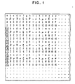
- Fig. 1 symbolically illustrates a two-dimensional array notation of data bits for a 1Kx1K bit array.
- Fig. 2 symbolically illustrates the mapping of the data bits of the two-dimensional array of Fig. 1 into a plurality of memory chips.
- Fig. 3 is a schematic block diagram of an on-chip address translation structure according to the principles of the present invention.
- Fig. 4 is a schematic block diagram of a memory to raster conversion scheme for serializing the output stream from a memory according to the principles of the present invention.
- Fig. 5 illustrates a two-dimensional array of data bits notation for 1
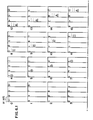
Kx 1 K, 1 Kx2K, 2Kx 1 K and 2Kx2K screens. - Figs. 6.1 and 6.2 symbolically illustrate the mapping of the data bits of the array of Fig. 5 into a 1 Kx2K screen with 32 chips and a 32 bit data path.
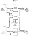
- Fig. 7 is a schematic block diagram of the hardware for implementing the mapping of Fig. 6.
- Figs. 8.1 and 8.2 symbolically illustrate the data bits of the array of Fig. 5 into a 2Kx 1 K screen.
- Fig. 9 is a schematic block diagram of the hardware for implementing the mapping of Fig. 8.
- Fig. 10 is a schematic block diagram of the hardware for implementing the mapping of data bits into a 2Kx2K screen.
- There are many data processing applications that can be enhanced by the ability to write both horizontal and vertical lines into a two-dimensional array according to the present invention. The following describes a mapping for storing an array in 64K memory chips, and the required data transformations, address calculations, and chip hardware. As described, the mapping and hardware provide bit addressability in both horizontal and vertical directions. However, removal of the incrementer associated with the word and/or bit address will remove the bit addressability in the vertical and/or horizontal direction respectively, while still retaining the ability to write 16 bits beginning at even byte boundaries.
- Referring to Fig. 1, a two-dimensional array of data bits is illustrated and Fig. 2 shows the mapping of the array into the memory chips. It is seen that 16 horizontal bits are placed into corresponding locations in each chip with a bit increment for those chips associated with bits crossing an even byte boundary. The mapping of 16 vertical bits is somewhat more complicated, in that the bits are placed in corresponding locations in quadrants of different words. The quadrants increase by 1
modulo 4 and the words increase by 1 each time the quadrant becomes 0. This sequencing through quadrants and words is best described by associating a 4 bit quantity with location where the 2 low order bits define the quadrant and the 2 high order bits define the 2 low order bits of the word address. Sequencing through the locations then corresponds to sequencing through theconsecutive numbers 0 to 15. For those bits that cross an even byte boundary, the word address must be increased by four. The important observation to be made about the mapping is that 16 horizontal or vertical bits can be written into memory in one cycle because no two bits are mapped to the same chip. - Given that 16 horizontal or 16 vertical bits can be mapped into the memory in one write cycle, the next important question is the computational complexity and the amount of additional hardware required. This complexity and hardware is required for address calculation and data manipulation, on-chip address translation, and memory to raster-scan conversion.
- The functions to be performed by the address generation chip are given by the following equations where X, Y is the screen address; mode and bit and word addresses are broadcast to all chips; and each chip receives the appropriate data, mask and increment signal:
- Horizontal mode:
- Bit-address (5,4,3,2,1,0)=integer of X/16 or X(9,8,7,6,5,4)
- Bit-address (7,6)=4 modulo Y or Y(1,0)
- Word-address (1,0)=4 modulo integer of Y/4 or Y(3,2)
- Word-address (7,6,5,4,3,2)=integer of Y/16 or Y(9,8,7,6,5,4)
- Data=16 modulo (X+Y) rotate of 16 take Data
- Mask=16 modulo (X+Y) rotate of 16
take #Data 1's
- Bit increment=16 modulo (X+Y) rotate of ((16-161X) number of zeros followed by (16!X) number of ones.
- The "16 take" can be deleted if it is assumed that 16 bits of data are always received. The term "16 take" indicates that the user may want to write less than 16 bits.
- Word-increment=0
- Mode=0
- The address of the first bit in the vertical line is the same as that calculated in the horizontal mode. However, this bit is in
chip # 16 modulo (X+Y). Since the address modification in the chip adds the chip # to the portion of the address WL, BH, that portion of the address must be decreased by 16 modulo (X+Y) before being broadcast to all chips. With this modification the address modification equations become: - Bit-address (5,4,3,2,1,0)=Integer of X/16 or X(9,8,7,6,5,4)
- Bit-address (7,6)=4 modulo Y-16 modulo (X+Y) =4 modulo -X
- Word-address (1,0)=4 modulo ((4x4iinteger part of Y/4)-161(X+Y))/4 =4 modulo (16:Y-16 (X+Y))/4 =4 modulo integer of -X/4
- Word-address (7,6,5,4,3,2)=integer of Y/16 or Y(9,8,7,6,5,4)
- Data=16 modulo (X+Y) rotate of 16 take Data
- Mask=16 modulo (X+Y) rotate of 16
take #Data 1's - Word-increment=16 modulo (X+Y) rotate of ((16-16 Y)p0), (16Y)p1
- Note that this is the same function as the bit increment above with the appropriate change of X to Y. Bit-increment=0 Mode=
- Fig. 3 shows the on-chip hardware required for address translation. The translation affects only the two low order bits of the word address and the two high order bits of the bit address. The function performed is an addition of the 4 bit chip number from the chip number storage to the four bits formed by concatenating BH and WL where BH is the two low order bits and WL is the two high order bits which are applied as inputs to the adder. The four bit result of the addition (ignoring carry out) is also the concatenation of BH and WL in the same order as in the input. The six higher order bits of the word address and the six lower order bits of the bit address are applied to respective incrementer circuits as illustrated. It should be noted that the portion of the word and bit address that may be altered by their respective incrementers are disjoint from the portion that is modified by the 4 bit adder. Therefore, the incrementers can be removed independently from the remainder of the address translation hardware. Thus, a modified scheme can be implemented in which writing starts only on even byte boundaries in either or both horizontal and vertical directions. Further, it should be noted that the incrementer can be shared since at most, one of them is active during a given write operation. The four bits that identify the chip position or number can be either on-chip storage as shown, or signal pins that are connected to the appropriate signals. It should be noted that in mode=0, the adder receives 0 from chip number storage. The adder and the incrementer circuits used in the structure of Fig. 3 are conventional state-of-the-art devices.
- Fig. 4 shows the scheme necessary for serializing the output bit stream. The only modification to the typical raster generation scheme of the prior art is the addition of hardware that increments the serializer position once after each scan line in order to account for the staggered storage pattern. Each READ into the output buffer provides enough data for four scan lines. These bits are scanned successively in the bit direction with the origin within the 16. buffers being incremented modulo 16 after every scan line.
- The screen signals are obtained from row buffer storage devices (i.e., 256 bit row buffer in the specific example of Fig. 4). The 16 chip row buffers will contain the first four scan lines of the 1Kx1K display. The scan lines are stored in a manner that provides easy access as indicated by the bit coordinate shown in Fig. 4.
- Figs. 1 through 4 relate to mapping and memory hardware for writing horizontal and vertical lines for a 1 Kx 1 K screen. In the present invention, the mapping can be extended to any of four screen sizes obtained by doubling one or both of the dimensions (i.e., 1 Kx2K, 2Kx 1 K and 2Kx2K). This mapping effectively uses the same hardware described in Figs. 3 and 4 with slight modification.
- Fig. 5 shows the notation that describes the picture elements (pels) on the screen. This notation is used to show the placement of the pels in the memory chips for the different mappings.
- Fig. 6 shows the mapping extended to a 1Kx2K screen with 32 chips and a 32 bit data path. It is seen that the mapping is similar to the 1 Kx 1 K mapping except that the word modularity is 8 rather than 4. This mapping is almost like the original except that 32 bits are written simultaneously.
- Fig. 7 illustrates the hardware for the lKx2K mapping embodiment. The only modification from the 1 Kx 1 K hardware is that the adder is now 5 bits and an extra chip number bit and one additional lower order bit of the word address are passed through it.
- Fig. 8 shows the mapping for a 2Kx 1 K screen. Here the modularity in the bit dimension is double. It is seen that the adder is 5 bits and an extra chip number bit and one additional bit of the bit address are sent through it.
- Fig. 9 illustrates the hardware for the mapping for a 2Kx1K screen. The only modification over the hardware of Fig. 7 is that two lower order word address bits and three higher order bit address bits are applied to the adder, six bits are applied to the word address incrementer and five bits are applied to the bit address incrementer, with corresponding variations in the outputs.
- Fig. 10 illustrates the modification of the hardware for mapping a 2Kx2K screen. It is noted that the difference over Fig. 9 is that three lower order bits of the word address are applied to the adder along with the three high order bits of the bit address. Consequently, the chip number storage provides six bits to the adder. It should be noted that in Mode=0, the adder receives 0 from chip number storage.
- In another modification of the present invention, the multiplexing of addresses may be employed. In prior art systems it is known that the horizontal word address may be followed by a series of bit addresses. In the present invention, the same technique can be utilized, with the further novel aspect that in addition to the word address being followed by a series of bit addresses for the horizontal case, the bit address can be applied followed by a series of word addresses in the vertical case.
- In such an embodiment, the structure of Figs. 3, 7, 9 and 10 is modified in that only one incrementer means is used with both the "word inc" signal and the "bit inc" signal being applied to the one incrementer in a time shared manner. Thus, in the mode wherein a word address is applied followed by a series of bit addresses, the "word inc" signal is applied first. When a bit address is applied followed by a series of word addresses, the "bit inc" signal is applied first.
- What has been described is structure for entering horizontal and vertical bit strings into a two-dimensional computer memory. The invention is useful for use in display systems wherein mapping from a frame buffer to a high function raster-scan display screen is enhanced by the described structure for writing either vertical bit strings or horizontal bit strings.
- The invention was described as including a plurality of separate memory chips. One skilled in the art will appreciate that each of the discrete memory locations required may, along with their associated circuits, be fabricated onto a single master chip.
Claims (2)
characterised in that data word addresses have a high word address portion and a low word address portion (WL) and data bit addresses have a high bit address portion (BH) and a low bit address portion and said storage means includes address generator means (Fig. 3) for address translation having a horizontal and a vertical mode of operation and including at least one incremeter incrementing said high word address portion and incrementing said low bit address portion, a chip number storage means for providing chip number bits and an adder, wherein said low word address portion (WL) and said high bit address portion (BH) are concatenated at the adder input and, in the vertical mode, the chip number is added to the concatenated bits and the adder output is combined with the output of said incrementer to produce a translated data word address and a translated data bit address, whereby the adder output is divided, on the one hand, into high order bits corresponding to said low word address portion (WL), and, on the other hand, into low order bits corresponding to said high bit address portion (BH), and said high order bits are concatenated with said high word address portion and said low order bits are concatenated with said low bit address portion.
Applications Claiming Priority (2)
| Application Number | Priority Date | Filing Date | Title |
|---|---|---|---|
| US06/509,697 US4559611A (en) | 1983-06-30 | 1983-06-30 | Mapping and memory hardware for writing horizontal and vertical lines |
| US509697 | 1983-06-30 |
Publications (3)
| Publication Number | Publication Date |
|---|---|
| EP0130340A2 EP0130340A2 (en) | 1985-01-09 |
| EP0130340A3 EP0130340A3 (en) | 1987-11-25 |
| EP0130340B1 true EP0130340B1 (en) | 1990-09-12 |
Family
ID=24027734
Family Applications (1)
| Application Number | Title | Priority Date | Filing Date |
|---|---|---|---|
| EP84105759A Expired EP0130340B1 (en) | 1983-06-30 | 1984-05-21 | Memory mapping and readout system |
Country Status (4)
| Country | Link |
|---|---|
| US (1) | US4559611A (en) |
| EP (1) | EP0130340B1 (en) |
| JP (1) | JPS6015688A (en) |
| DE (1) | DE3483181D1 (en) |
Families Citing this family (6)
| Publication number | Priority date | Publication date | Assignee | Title |
|---|---|---|---|---|
| FR2566950B1 (en) * | 1984-06-29 | 1986-12-26 | Texas Instruments France | VIDEO IMAGE POINT PROCESSOR, VIEWING SYSTEM COMPRISING APPLICATION AND METHOD FOR IMPLEMENTING SAME |
| US4912658A (en) * | 1986-04-18 | 1990-03-27 | Advanced Micro Devices, Inc. | Method and apparatus for addressing video RAMS and refreshing a video monitor with a variable resolution |
| US4716546A (en) * | 1986-07-30 | 1987-12-29 | International Business Machines Corporation | Memory organization for vertical and horizontal vectors in a raster scan display system |
| JPS63177235A (en) * | 1987-01-19 | 1988-07-21 | Fujitsu Ltd | Multi-dimension access memory |
| GB2250615B (en) * | 1990-11-21 | 1995-06-14 | Apple Computer | Apparatus for performing direct memory access with stride |
| US5235613A (en) * | 1992-03-02 | 1993-08-10 | The Boeing Company | Frequency hopping method and apparatus |
Family Cites Families (18)
| Publication number | Priority date | Publication date | Assignee | Title |
|---|---|---|---|---|
| US3292151A (en) * | 1962-06-04 | 1966-12-13 | Ibm | Memory expansion |
| FR1543788A (en) * | 1966-12-28 | Ibm | Multi-word multidirectional random access memory system | |
| US3588829A (en) * | 1968-11-14 | 1971-06-28 | Ibm | Integrated memory system with block transfer to a buffer store |
| US3737866A (en) * | 1971-07-27 | 1973-06-05 | Data General Corp | Data storage and retrieval system |
| US4020470A (en) * | 1975-06-06 | 1977-04-26 | Ibm Corporation | Simultaneous addressing of different locations in a storage unit |
| US4024508A (en) * | 1975-06-19 | 1977-05-17 | Honeywell Information Systems, Inc. | Database instruction find serial |
| US4025901A (en) * | 1975-06-19 | 1977-05-24 | Honeywell Information Systems, Inc. | Database instruction find owner |
| US4090174A (en) * | 1976-11-01 | 1978-05-16 | International Business Machines Corporation | Method and apparatus for accessing horizontal sequences, vertical sequences and rectangular subarrays from an array stored in a modified word organized random access memory system |
| US4126897A (en) * | 1977-07-05 | 1978-11-21 | International Business Machines Corporation | Request forwarding system |
| US4128873A (en) * | 1977-09-20 | 1978-12-05 | Burroughs Corporation | Structure for an easily testable single chip calculator/controller |
| US4195342A (en) * | 1977-12-22 | 1980-03-25 | Honeywell Information Systems Inc. | Multi-configurable cache store system |
| US4296467A (en) * | 1978-07-03 | 1981-10-20 | Honeywell Information Systems Inc. | Rotating chip selection technique and apparatus |
| US4309755A (en) * | 1979-08-22 | 1982-01-05 | Bell Telephone Laboratories, Incorporated | Computer input/output arrangement for enabling a simultaneous read/write data transfer |
| JPS56118145A (en) * | 1980-02-22 | 1981-09-17 | Ricoh Co Ltd | Processor for video information |
| DE3015125A1 (en) * | 1980-04-19 | 1981-10-22 | Ibm Deutschland Gmbh, 7000 Stuttgart | DEVICE FOR STORING AND DISPLAYING GRAPHIC INFORMATION |
| US4370732A (en) * | 1980-09-15 | 1983-01-25 | Ibm Corporation | Skewed matrix address generator |
| JPS5784486A (en) * | 1980-11-13 | 1982-05-26 | Usac Denshi Kogyo Kk | Character generator |
| US4402043A (en) * | 1980-11-24 | 1983-08-30 | Texas Instruments Incorporated | Microprocessor with compressed control ROM |
-
1983
- 1983-06-30 US US06/509,697 patent/US4559611A/en not_active Expired - Lifetime
-
1984
- 1984-03-19 JP JP59051295A patent/JPS6015688A/en active Pending
- 1984-05-21 DE DE8484105759T patent/DE3483181D1/en not_active Expired - Fee Related
- 1984-05-21 EP EP84105759A patent/EP0130340B1/en not_active Expired
Also Published As
| Publication number | Publication date |
|---|---|
| US4559611A (en) | 1985-12-17 |
| EP0130340A3 (en) | 1987-11-25 |
| EP0130340A2 (en) | 1985-01-09 |
| DE3483181D1 (en) | 1990-10-18 |
| JPS6015688A (en) | 1985-01-26 |
Similar Documents
| Publication | Publication Date | Title |
|---|---|---|
| EP0225059B1 (en) | Semiconductor memory | |
| EP0492939B1 (en) | Method and apparatus for arranging access of VRAM to provide accelerated writing of vertical lines to an output display | |
| US5321510A (en) | Serial video processor | |
| US4561072A (en) | Memory system handling a plurality of bits as a unit to be processed | |
| CA2027458A1 (en) | Method to rotate a bit map image 90 degrees | |
| JP3278756B2 (en) | Image processing method and apparatus | |
| EP0744712A2 (en) | A texture pattern memory circuit | |
| KR910002202B1 (en) | Boundary-free conductor | |
| US5361339A (en) | Circuit for fast page mode addressing of a RAM with multiplexed row and column address lines | |
| EP0130340B1 (en) | Memory mapping and readout system | |
| US5230064A (en) | High resolution graphic display organization | |
| GB2174277A (en) | Method and system for displaying multiple images on a display screen | |
| US5412740A (en) | Signal processing system having reduced memory space | |
| US6085304A (en) | Interface for processing element array | |
| EP0367995B1 (en) | Vector data transfer controller | |
| US5008852A (en) | Parallel accessible memory device | |
| JPH06167958A (en) | Memory device | |
| US6680736B1 (en) | Graphic display systems having paired memory arrays therein that can be row accessed with 2(2n) degrees of freedom | |
| US4888584A (en) | Vector pattern processing circuit for bit map display system | |
| Ericsson et al. | LIPP-A SIMD multiprocessor architecture for image processing | |
| EP0549309A1 (en) | Address reduction scheme implementing rotation algorithm | |
| JPH028335B2 (en) | ||
| JP2633251B2 (en) | Image memory device | |
| JPH03196376A (en) | Addressing mechanism for parallel access to a plurality of adjacent storage positions from the whole field storage devices | |
| JPS62151987A (en) | Multi port memory processing picture |
Legal Events
| Date | Code | Title | Description |
|---|---|---|---|
| PUAI | Public reference made under article 153(3) epc to a published international application that has entered the european phase |
Free format text: ORIGINAL CODE: 0009012 |
|
| AK | Designated contracting states |
Designated state(s): DE FR GB |
|
| 17P | Request for examination filed |
Effective date: 19841123 |
|
| PUAL | Search report despatched |
Free format text: ORIGINAL CODE: 0009013 |
|
| AK | Designated contracting states |
Kind code of ref document: A3 Designated state(s): DE FR GB |
|
| 17Q | First examination report despatched |
Effective date: 19880511 |
|
| GRAA | (expected) grant |
Free format text: ORIGINAL CODE: 0009210 |
|
| AK | Designated contracting states |
Kind code of ref document: B1 Designated state(s): DE FR GB |
|
| REF | Corresponds to: |
Ref document number: 3483181 Country of ref document: DE Date of ref document: 19901018 |
|
| ET | Fr: translation filed | ||
| PLBE | No opposition filed within time limit |
Free format text: ORIGINAL CODE: 0009261 |
|
| STAA | Information on the status of an ep patent application or granted ep patent |
Free format text: STATUS: NO OPPOSITION FILED WITHIN TIME LIMIT |
|
| 26N | No opposition filed | ||
| PGFP | Annual fee paid to national office [announced via postgrant information from national office to epo] |
Ref country code: GB Payment date: 19940415 Year of fee payment: 11 |
|
| PGFP | Annual fee paid to national office [announced via postgrant information from national office to epo] |
Ref country code: FR Payment date: 19940427 Year of fee payment: 11 |
|
| PGFP | Annual fee paid to national office [announced via postgrant information from national office to epo] |
Ref country code: DE Payment date: 19940513 Year of fee payment: 11 |
|
| PG25 | Lapsed in a contracting state [announced via postgrant information from national office to epo] |
Ref country code: GB Effective date: 19950521 |
|
| GBPC | Gb: european patent ceased through non-payment of renewal fee |
Effective date: 19950521 |
|
| PG25 | Lapsed in a contracting state [announced via postgrant information from national office to epo] |
Ref country code: DE Effective date: 19960201 |
|
| PG25 | Lapsed in a contracting state [announced via postgrant information from national office to epo] |
Ref country code: FR Effective date: 19960229 |
|
| REG | Reference to a national code |
Ref country code: FR Ref legal event code: ST |
|
| REG | Reference to a national code |
Ref country code: FR Ref legal event code: ST |