EP0129054A1 - Circuitry comprising a data memory and a control unit for reading, writing and erasing the memory - Google Patents
Circuitry comprising a data memory and a control unit for reading, writing and erasing the memory Download PDFInfo
- Publication number
- EP0129054A1 EP0129054A1 EP84105461A EP84105461A EP0129054A1 EP 0129054 A1 EP0129054 A1 EP 0129054A1 EP 84105461 A EP84105461 A EP 84105461A EP 84105461 A EP84105461 A EP 84105461A EP 0129054 A1 EP0129054 A1 EP 0129054A1
- Authority
- EP
- European Patent Office
- Prior art keywords
- memory
- data memory
- signal
- data
- circuit arrangement
- Prior art date
- Legal status (The legal status is an assumption and is not a legal conclusion. Google has not performed a legal analysis and makes no representation as to the accuracy of the status listed.)
- Ceased
Links
Images


Classifications
-
- G—PHYSICS
- G07—CHECKING-DEVICES
- G07F—COIN-FREED OR LIKE APPARATUS
- G07F7/00—Mechanisms actuated by objects other than coins to free or to actuate vending, hiring, coin or paper currency dispensing or refunding apparatus
- G07F7/08—Mechanisms actuated by objects other than coins to free or to actuate vending, hiring, coin or paper currency dispensing or refunding apparatus by coded identity card or credit card or other personal identification means
- G07F7/10—Mechanisms actuated by objects other than coins to free or to actuate vending, hiring, coin or paper currency dispensing or refunding apparatus by coded identity card or credit card or other personal identification means together with a coded signal, e.g. in the form of personal identification information, like personal identification number [PIN] or biometric data
- G07F7/1008—Active credit-cards provided with means to personalise their use, e.g. with PIN-introduction/comparison system
-
- G—PHYSICS
- G06—COMPUTING; CALCULATING OR COUNTING
- G06Q—INFORMATION AND COMMUNICATION TECHNOLOGY [ICT] SPECIALLY ADAPTED FOR ADMINISTRATIVE, COMMERCIAL, FINANCIAL, MANAGERIAL OR SUPERVISORY PURPOSES; SYSTEMS OR METHODS SPECIALLY ADAPTED FOR ADMINISTRATIVE, COMMERCIAL, FINANCIAL, MANAGERIAL OR SUPERVISORY PURPOSES, NOT OTHERWISE PROVIDED FOR
- G06Q20/00—Payment architectures, schemes or protocols
- G06Q20/30—Payment architectures, schemes or protocols characterised by the use of specific devices or networks
- G06Q20/34—Payment architectures, schemes or protocols characterised by the use of specific devices or networks using cards, e.g. integrated circuit [IC] cards or magnetic cards
- G06Q20/341—Active cards, i.e. cards including their own processing means, e.g. including an IC or chip
-
- G—PHYSICS
- G06—COMPUTING; CALCULATING OR COUNTING
- G06Q—INFORMATION AND COMMUNICATION TECHNOLOGY [ICT] SPECIALLY ADAPTED FOR ADMINISTRATIVE, COMMERCIAL, FINANCIAL, MANAGERIAL OR SUPERVISORY PURPOSES; SYSTEMS OR METHODS SPECIALLY ADAPTED FOR ADMINISTRATIVE, COMMERCIAL, FINANCIAL, MANAGERIAL OR SUPERVISORY PURPOSES, NOT OTHERWISE PROVIDED FOR
- G06Q20/00—Payment architectures, schemes or protocols
- G06Q20/30—Payment architectures, schemes or protocols characterised by the use of specific devices or networks
- G06Q20/34—Payment architectures, schemes or protocols characterised by the use of specific devices or networks using cards, e.g. integrated circuit [IC] cards or magnetic cards
- G06Q20/357—Cards having a plurality of specified features
-
- G—PHYSICS
- G07—CHECKING-DEVICES
- G07F—COIN-FREED OR LIKE APPARATUS
- G07F7/00—Mechanisms actuated by objects other than coins to free or to actuate vending, hiring, coin or paper currency dispensing or refunding apparatus
- G07F7/08—Mechanisms actuated by objects other than coins to free or to actuate vending, hiring, coin or paper currency dispensing or refunding apparatus by coded identity card or credit card or other personal identification means
- G07F7/0866—Mechanisms actuated by objects other than coins to free or to actuate vending, hiring, coin or paper currency dispensing or refunding apparatus by coded identity card or credit card or other personal identification means by active credit-cards adapted therefor
-
- G—PHYSICS
- G11—INFORMATION STORAGE
- G11C—STATIC STORES
- G11C16/00—Erasable programmable read-only memories
- G11C16/02—Erasable programmable read-only memories electrically programmable
- G11C16/06—Auxiliary circuits, e.g. for writing into memory
- G11C16/10—Programming or data input circuits
-
- G—PHYSICS
- G11—INFORMATION STORAGE
- G11C—STATIC STORES
- G11C16/00—Erasable programmable read-only memories
- G11C16/02—Erasable programmable read-only memories electrically programmable
- G11C16/06—Auxiliary circuits, e.g. for writing into memory
- G11C16/32—Timing circuits
Landscapes
- Engineering & Computer Science (AREA)
- Business, Economics & Management (AREA)
- Physics & Mathematics (AREA)
- General Physics & Mathematics (AREA)
- Microelectronics & Electronic Packaging (AREA)
- Computer Networks & Wireless Communication (AREA)
- Accounting & Taxation (AREA)
- Strategic Management (AREA)
- General Business, Economics & Management (AREA)
- Theoretical Computer Science (AREA)
- Read Only Memory (AREA)
- Storage Device Security (AREA)
Abstract
Um die Speichereigenschaften eines elektrisch löschbaren, programmierbaren Datenspeichers (8) ("lesbar", "löschbar", "schreibbar") auf einfache Weise flexibel an unterschiedliche Anforderungen anzupassen, weist die Schaltungsanordnung einen Funktionsdatenspeicher (5) auf, dessen Speicherzeilen über einen Adreßdekoder (4) gemeinsam mit den Speicherzellen des Datenspeichers (8) adressierbar sind. Die Ausgänge des Funktionsdatenspeichers (5) sind über eine Verknüpfungseinheit (6) mit einer Ansteuerschaltung (2, 7) zum Schreiben, Lesen, und Löschen des Datenspeichers (8) verbunden. Abhängig von der Programmierung des Funktionsdatenspeichers (5) wird die Wirksamkeit eines Löschsignals (LOE), eines Schreibsignals (SCHR) und/oder eines Lesesignals (LES) aufgehoben.In order to adapt the storage properties of an electrically erasable, programmable data memory (8) ("readable", "erasable", "writable") flexibly to different requirements in a simple manner, the circuit arrangement has a functional data memory (5), the memory lines of which are addressed via an address decoder ( 4) can be addressed together with the memory cells of the data memory (8). The outputs of the function data memory (5) are connected via a logic unit (6) to a control circuit (2, 7) for writing, reading and deleting the data memory (8). Depending on the programming of the function data memory (5), the effectiveness of a delete signal (LOE), a write signal (SCHR) and / or a read signal (LES) is canceled.
Description
Die Erfindung betrifft eine Schaltungsanordnung, bestehend aus einem Datenspeicher mit nichtflüchtigen, elektrisch schreib- und löschbaren Speicherzellen, aus einem Adreßdekoder und aus einer Ansteuereinheit zum Auslesen, Schreiben und Löschen von Teilbereichen des Speichers.The invention relates to a circuit arrangement consisting of a data memory with non-volatile, electrically writable and erasable memory cells, an address decoder and a control unit for reading, writing and deleting partial areas of the memory.
Aus der Zeitschrift "Electronics" ist ein Zeilen und spaltenweise adressierbarer Datenspeicher bekannt, welcher über eine Ansteuerschaltung elektrisch auslesbar, beschreibbar und löschbar ist. Die Speicherbeschreibung wurde von W.S. Johnson, G.L. Kuhn, A.L. Renninger und D. Perlegos unter dem Titel: "16-kEE-PROM relies on tunneling for byte-erasable program storage" im Heft February 28, 1980, Seite 113 ff. veröffentlicht. Es gibt jedoch Ahwendungen für einen derartigen Speicher, bei welchen es wünschenswert ist, neben einem bezüglich der Funktionseigenschaften uneingeschränkten Adreßbereich auch Speicherbereiche mit eingeschränkten Funktionseigenschaften zur Verfügung zu haben. Diese Forderung besteht beispielsweise dann, wenn der Speicher in datengesteuerten Zahlungssystemen zum bargeldlosen Bezahlen von Waren oder zum Abrechnen von Dienstleistungen und ähnlichem eingesetzt ist. Zahlungssysteme dieser Art sind in der Zeitschrift "Betriebspraxis", B.BL. 2/1982, S. 48 ff. von Dr. R.Novak und W. Roeder unter dem Titel "Die Chipkarte - nächste Generation der Automatenkarte" beschrieben. Die dabei verwendeten Karten tragen als ein wesentliches Element einen nichtflüchtigen elektrischen Datenspeicher, auf den über elektrische Kontakte an der Kartenoberfläche zugegriffen werden kann. Über ein Kartenlesegerät wird von einer Recheneinheit bei jedem Gebrauch auf den Speicherinhalt zugegriffen , der dabei gegebenenfalls geändert wird.From the magazine "Electronics" a row and column-wise addressable data memory is known, which can be read, written and erased electrically via a control circuit. The memory description was published by WS Johnson, GL Kuhn, AL Renninger and D. Perlegos under the title: "16-kEE-PROM relies on tunneling for byte-erasable program storage" in February 28, 1980, page 113 ff. However, there are applications for such a memory in which it is desirable to have memory areas with restricted functional properties in addition to an address area which is unrestricted with regard to the functional properties. This requirement exists, for example, when the memory is used in data-controlled payment systems for cashless payment for goods or for billing services and the like. Payment systems of this type are described in the journal "Betriebsspraxis", B.BL. 2/1982, p. 48 ff. By Dr. R.Novak and W. Roeder under the title "The chip card - next generation of the automatic card". The cards used carry one as an essential element non-volatile electrical data storage that can be accessed via electrical contacts on the card surface. Each time a computing unit is used, a computing unit accesses the memory content via a card reader, which is changed if necessary.
Zur Anwendung kommen derartige Karten in Sicherheits- und Zugriffssystemen, in Abrechnungs- oder Registriersystemen und in Debit- oder Kreditsystemen. Um eine weite Verbreitung und häufigen Gebrauch der Karten zu gewährleisten, gibt es Betreiber solcher Systeme, die eine Vielzahl von Karten ausgeben, und die ein weitverzweigtes Netz von Lesegeräten und Rechenanlagen anbieten. Um Mißbräuche der Daten auszuschließen, müssen hohe Sicherheitsforderungen an die Kartensysteme gestellt werden. Besonders die Trägerkarten, deren Verbreitung nicht immer kontrollierbar ist, müssen vor einer Benutzung durch Unberechtigte geschützt werden.Cards of this type are used in security and access systems, in accounting or registration systems and in debit or credit systems. In order to ensure widespread and frequent use of the cards, there are operators of such systems which issue a large number of cards and which offer an extensive network of reading devices and computing systems. To prevent misuse of the data, high security requirements must be placed on the card systems. Carrier cards in particular, the distribution of which cannot always be controlled, must be protected against unauthorized use.
Dies kann durch eine Freigabeoperation erreicht werden, bei welcher ein Datenvergleich zwischen einem van -eiher Bedienungsperson eingegebenen oder von einer Rechenanlage verschlüsselten Code-Wort mit einem abgespeicherten Referenzwort durchgeführt wird, und abhängig vom Vergleichsergebnis der Zugriff freigegeben bzw. unterbunden wird. Während der Freigabeoperation soll einerseits der Zugriff auf einen vorbestimmten Adreßbereiqh des Speichers möglich sein, aber andererseits der Zugriff auf einen mit geheimen oder zu schützenden Daten belegten Anwenderdatenbereich gesperrt sein.This can be achieved by a release operation in which a data comparison is carried out between a code word entered by an operator or encrypted by a computer system with a stored reference word, and access is enabled or prevented depending on the comparison result. During the release operation, on the one hand, access to a predetermined address area of the memory should be possible, but on the other hand, access to a user data area occupied by secret data or data to be protected should be blocked.
Dabei kann abhängig vom Anwendungsfall des Speichers ein Löschen, Beschreiben oder Auslesen des Anwenderdatenbereichs ohne erfolgreiche Durchführung der Freigabeoperation unterbunden sein. Ein weiterer Speicherbereich, der zur Aufnahme der geheimen Referenzdaten dient, kann darüberhinaus unter allen Umständen gegen Auslesen in ein extern auslesbares Register geschützt sein.Depending on the application of the memory, deletion, writing or reading out of the user data area can be prevented without successfully carrying out the release operation. Another storage area that is used for Recording of the secret reference data can also be protected against reading into an externally readable register under all circumstances.
Zur Zwischenspeicherung von Daten, die während der Freigabeoperation enstehen, kann ein dritter Speicherbereich mit variierbaren oder zustandsabhängigen Zugriffssperren versehen sein. Eine Freigabeoperation, welche beispielsweise einen Datenvergleich und ein davon abhängiges Beschreiben und gegebenenfalls Löschen dieses dritten Speicherbereichs erfordert, wird folglich abhängig vom Verlauf der Freigabeoperation nacheinander mit einer Schreib-und Löschsperre beaufschlagbar sein, die nur bei ordungsgemäßem Ablauf der Freigabeoperation aufhebbar sind.A third memory area can be provided with variable or status-dependent access locks for the temporary storage of data which arise during the release operation. A release operation, which requires, for example, a data comparison and a description and, if necessary, deletion of this third memory area, will consequently, depending on the course of the release operation, be able to be acted upon successively with a write and delete lock, which can only be released if the release operation is carried out properly.
Die optimale Aufteilung eines Speichers in Bereiche unterschiedlicher Eigenschaften hängt von der Anwendung selbst und von den jeweiligen Sicherheitsanforderungen ab. Der Erfindung lag daher die Aufgabe zugrunde, eine Schaltungsanordnung der oben genannten Art anzugeben, mit welcher auf einfache Weise eine flexible Anpassung der Speichereigenschaften an die gewünschten Anforderungen möglich ist.The optimal division of a memory into areas with different properties depends on the application itself and the respective security requirements. The invention was therefore based on the object of specifying a circuit arrangement of the type mentioned above, with which a flexible adaptation of the memory properties to the desired requirements is possible in a simple manner.
Diese Aufgabe wird durch einEnFunktionadatenspeicher gelöst, dessen Speicherzellen gemeinsam mit den Speicherzellen des Datenspeichers adressierbar sind, und durch eine Verknüpfungseinheit über welche der Funktionsdatenspeicher ausgangsseitig mit der Ansteuerschaltung verbunden ist.This object is achieved by a nFunktionadatenspeicher E, whose memory cells are addressable in common with the memory cells of the data memory, and is connected on the output side by a linking unit via which the data storage function to the drive circuit.
Auf diese Weise wird eine Adreßabhängigkeit der Funktionseigenschaften "lesbar", "schreibbar", und "löschbar" des Datenspeichers erreicht. Durch eine Programmierung des Funktionsdatenspeicherss werden also Speicherbereiche des Datenspeichers festgelegt, welche beispielsweise die Eigenschaften eines elektrisch löschbaren, programmierbaren Speichers (EEPROM), eines programmierbaren Speichers (PROM) oder eines Nur-Lesespeichers (RON) aufweisen.In this way an address dependency of the functional properties "readable", "writable" and "erasable" of the data memory is achieved. By programming the functional data memory, memory areas of the data memory are defined, which for example have the properties of an electrically erasable, programmable Have memory (EEPROM), a programmable memory (PROM) or a read-only memory (RON).
Weiterbildungen der Erfindung ergeben sich aus den Unteransprüchen.Further developments of the invention result from the subclaims.
Im folgnden wird die Erfindung anhand eines Ausführungsbeispiels weiter beschrieben.
- Fig. 1 zeigt ein Blockschaltbild der Schaltungsanordnung
- Fig. 2 zeigt beispielhaft Einzelheiten der Schaltungsanordnung nach Fig. 1
- Fig. 3 zeigt für eine beispielhafte Belegung des Funktions datenspeichers in tabellarischer Form die Funktionseigenschaften von Speicherbereichen des Datenspeichers nach den Fig. 1 und 2.
- Fig. 1 shows a block diagram of the circuit arrangement
- FIG. 2 shows details of the circuit arrangement according to FIG. 1 by way of example
- 3 shows the functional properties of memory areas of the data memory according to FIGS. 1 and 2 for an exemplary assignment of the functional data memory in tabular form.
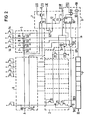
Die monolithisch integrierbare Schaltungsanordnung in Fig. 1 ist beispielsweise zur Verwendung in einem bargeldlosen Zahlungssystem, wie es eingangs Beschrieben ist auf einer Trägerkarte aufgebracht. Über je eine Dateneingangs- und Datenausgangsleitung DE und DA erfolgt ein serieller Datenaustausch mit einer nicht wiedergegebenen Recheneinheit. Die binär kodierten Bitfolgen werden dabei von einem Register 1, bestehend aus einem Adreßregister 1' und einem Datenregister 1'', aufgenommen. Eine auf die Datenausgangsleitung DA wirkende Auslesesperre 9 macht das Auslesen von Daten aus dem Register 1 von einem Ausgangssignal eines Funktionsdatenspeichers 5 und von einem Freigabesignals FREI abhängig. Dieses wird nach der erfolgreichen Durchführung einer Freigabeoperation, d.h. nach dem Vergleich von eingegebenen Code und abgespeicherten Referenzdaten, in einer nicht wiedergegebener Prüfschaltung erzeugt.The monolithically integrable circuit arrangement in FIG. 1 is applied, for example, to a carrier card for use in a cashless payment system, as described at the beginning. A serial data exchange with a non-reproduced computing unit takes place via a data input and data output line DE and DA. The binary-coded bit sequences are received by a
Mit 8 ist ein zeilen- und spaltenweise adressierbarer Datenspeicher mit nichtflüchtigen, elektrisch schreib-und löschbaren Speicherzellen bezeichnet. Die Adressierung erfolgt über einen Adreßdekoder 4, welcher eingangsseitig mit dem Adreßregister 1' verbunden ist. Ein zeilen- und spaltenweise organisierter Funktionsdatenspeicher 5 wird ebenfalls vom Adreßdekoder 4 gemeinsam mit dem Datenspeicher 8 adressiert.8 designates a data memory that can be addressed in rows and columns with non-volatile, electrically writable and erasable memory cells. Addressing takes place via an address decoder 4, which is connected on the input side to the address register 1 '. A row and column organized
Dabei wird über eine Bitfolge im Adreßregister 1' ein erster Speicherbereich im Datenspeicher 8, beispielsweise zur Aufnahme eines Datenwortes, zusammen mit einem zweiten Speicherbereich im Funktionsdatenspeicher 5, der zur Aufnahme von ein oder mehreren Bits ausgebildet sein kann, adressiert. Der Inhalt des zweiten Speicherbereichs bestimmt über eine Verknüpfungseinheit 6 inwieweit ein Lese-, Schreib- oder Löschsignal LES, SCHR, LOE wirksam werden. Über den Inhalt des Funktionsdatenspeichers ist somit der entsprechende Speicherplatz im Datenspeicher 8 bezüglich seiner Speichereigenschaften festgelegt.In this case, a first memory area in the data memory 8, for example for holding a data word, is addressed via a bit sequence in the address register 1 ', together with a second memory area in the
Wie Fig. 2 zeigt, besteht der Datenspeicher 8 aus zeilen-und spaltenweise geordneten Speicherzellen mit jeweils einem Auswahl-MOS-FET 80 und einem Speicher-MOS-FET 81. Alle Steuereingänge der Auswahl-MOS-FET 80 einer Zeile sind jeweils über eine Adreßleitung A mit dem Adreßdekoder 4 verbunden. Die Speicher-MOS-FETs 81 sind über Programmierleitungen von der Zeilensteuerung 7 ansteuerbar. Die Spaltenleitungen zum Schreiben bzw. Auslesen der Speicherzellen sind über die hintereinander geschalteten gesteuerten Strecken der Auswahl-MOS-FETs 80 und der Speicher-MOS-FETs 81 mit einem niederen Bezugspotential von beispielsweise 0 V verbunden. In Hinsicht auf eine übersichtliche Darstellung sind lediglich eine Speicherzelle des Datenspeichers 8 und die dazugehörige Adreßleitung, Programmierleitung und Spaltenleitung in der Figur wiedergegeben.As FIG. 2 shows, the data memory 8 consists of memory cells arranged in rows and columns, each with a selection MOS-FET 80 and a memory MOS-FET 81. All control inputs of the selection MOS-FET 80 of a row are each via one Address line A connected to the address decoder 4. The memory MOS-FETs 81 can be controlled by the
Der Zugriff auf den Datenspeicher 8 erfolgt über eine Ansteuerschaltung 2,7 , bestehend aus einer Spaltensteuerung 2 und einer Zeilensteuerung 7.The data memory 8 is accessed via a
Um eine Speicherzelle zu löschen, wird der Signalpegel einer Programmierzeile auf ein hohes Bezugspotential, beispielsweise 20 V,erhöht und die dazugehörende Spaltenleitung mit dem niederen Bezugspotential verbunden. Das Beschreiben einer Speicherzelle erfolgt dadurch, daß die Programmierzeile mit dem niederen Bezugspotential beaufschlagt und die Spaltenleitung mit einem dem abzuspeichernden Datenmuster entsprechenden Signalpegel beaufschlagt wird. In der Figur sind die zur Ansteuerung des Speichers 7 benötigten Pegelwandler nicht eingezeichnet.In order to erase a memory cell, the signal level of a programming line is increased to a high reference potential, for example 20 V, and the associated column line is connected to the low reference potential. A memory cell is written by applying the low reference potential to the programming line and applying a signal level corresponding to the data pattern to be stored to the column line. The level converters required to actuate the
Die Spaltensteuerung 2 besteht bezüglich einer jeden Spaltenleitung aus einem als Diode wirkenden Ansteuerungs-MOS-FET 20 ,und weiteren MOS-FETs 21, 24. Die MOS-FETs 20 verbinden jeweils eine Spaltenleitung mit einem gemeinsamen Verbindungspunkt, welcher über einen als Spannungsteiler dienenden MOS-FET 22 mit der gesteuerten Strecke eines MOS-FET 23 verbunden ist.With respect to each column line, the column controller 2 consists of a drive MOS FET 20 acting as a diode, and further
Dessen gesteuerte Strecke ist ebenso wie die gesteuerte Strecke der MOS-FET's 21 mit der Verknüpfungseinheit 6 verbunden.Its controlled path, like the controlled path of the MOS-
Zum parallelen Einschreiben eines Datenwortes in den Datenspeicher 8 sind für jede Spaltenleitung Dateneingangsleitungen DES vorgesehen, über welche jeweils ein MOS-FET 24 ansteuerbar ist. Jeder MOS-FET 11 verbindet die gesteuerte Strecke des zugeordneten MOS-FET 21 mit dem niederen Bezugspotential.For parallel writing of a data word into the data memory 8, data input lines DES are provided for each column line, via which a MOS-
Außerhalb der Spaltensteuereinheit 2 ist jede Spaltenleitung über die gesteuerte Strecke eines MOS-FET 10 mit einer Datenausgangsleitung DAS verbunden, die zum Datenregister 1'' führt. Über mehrere Datenausgangsleitungen DAS ist ein Datenwort aus dem Speicher 8 parallel in das Datenregister 1'' übertragbar.Outside the column control unit 2, each column line is connected via the controlled path of a MOS-
Die Zeilensteuerung 7 besteht aus MOS-FET's 70,71,72, 73. Dazu ist zu bemerken, daß einer jeden Zeile des Datenspeichers 8 ein dem MOS-FET 70 entsprechender Transistor zugeordnet ist, während die MOS-FET's 71,72, 73 über einen gemeinsamen Verbindungspunkt allen Zeilen gemeinsam zugeordnet sind.The
Der MOS-FET 70 wird über die Adreßleitung A angesteuert, sobald die entsprechende Zeile des Datenspeichers 8 adressiert ist. Abhängig von einem Lese-Lösch- oder Schreibsignal LES, LOE, SCHR, wird der gemeinsame Verbindungspunkt über einen der MOS-FETs 71, 72 bzw. 73 mit einer Lesespannung ULES, dem hohen Bezugspotential bzw. dem niederen Bezugspotential verbunden.The MOS-FET 70 is controlled via the address line A as soon as the corresponding line of the data memory 8 has been addressed. Depending on a read-erase or write signal LES, LOE, SCHR, the common connection point is connected via one of the MOS-
Der Funk tions datens peicher 5 ist in dem Ausführungsbeispiel der Fig. 2 als maskenprogrammierbarer Speicher ausgeführt. Die Speicherzellen sind zeilen- und spaltenweise organisiert, wobei jeweils eine Zeile vier Speicher-MOS-FETs 50, 51 52, 53 aufweist. Jeweils einer dieser MOS-FETs ist einer ersten, zweiten, dritten bzw. vierten Spaltenleitung I, II, III, bzw. IV zugeordnet, die jeweils eingangsseitig über einen Last-MOS-FET 54 mit dem hohen Bezugspotential und ausgangsseitig mit der Verknüpfungseinheit 6 verbunden sind.The
Die gesteuerten Strecken der Speicher-MOS-FETs 50, 51, 52, 53 verbinden abhängig von der Speicherprogrammierung die zugeordnete Spaltenleitung mit dem niederen Bezugspotential. Ist aufgrund der Programmierung die gesteuerte Strecke eines oder mehrerer Speicher-MOS-FET's unterbrochen, so gilt die entsprechende Speicherzelle als gelöscht (Löschpegel log.1).The controlled paths of the
Ist der Funktionsdatenspeicher 5 beispielsweise ebenso wie der Datenspeicher 8 als elektrisch löschbarer, programmierbarer Speicher ausgebildet, so besteht jede Speicherzelle aus einem Adressier-MOS-FET und einem Speicher-MOS-FET, deren gesteuerte Strecken hintereinandergeschaltet die zugeordnete Spaltenleitung mit dem niederen Bezugspotential verbinden (nicht darstellt).If, for example, the
Die Steuereingänge der Speicher-MOS-FET's 50, 51, 52, 53 - im Fall eines maskenprogrammierbaren Speichers - bzw. der Adressier-MOS-FETs im Fall eines elektrisch löschbaren, programmierbaren Speichers sind in dem wiedergegebenen Beispiel wie der Datenspeicher 8 ebenfalls zeilenweise mit der Adressleitung A verbunden. Somit ist eine direkte Zuordnung des ersten Speicherbereichs im Datenspeicher 8 und des zweiten Speicherbereichs im Funktionsdatenspeicher 5 hergestellt.The control inputs of the memory MOS-
Die Verknüpfungseinheit 6 besteht aus einem NAND-Glied 60 und UND-Gliedern 61,62. Das UND-Glied 62 verbindet die Spaltenleitung IV und die mit dem Löschsignal LOE beaufschlagte Leitung mit dem Steuereingang des MOS-FET 72.The logic unit 6 consists of a NAND gate 60 and AND
Die Spaltenleitung II ist mit allen Steuereingängen der MOS-FET's 10 verbunden. Das NAND-Glied 60 liegt vor dem Steuereingang des MOS-FET's 23. An seinem Eingang liegt die erste Spaltenleitung I und die Leitung mit dem Schreibsignal SCHR. Die Spaltenleitung III führt auf den Setzeingang eines Flipflops 90. In der Auslesesperre 9 ist der Ausgang Q des Flip-Flops 90 zusammen mit einer Leitung, die mit dem Freigabesignal FREI beaufschlagbar ist, an ein ODER-Glied 91 gelegt. Dessen Ausgang führt zusammen mit der Datenausgangsleitung DA' auf ein UND-Glied 92, welches ausgangsseitig mit der Datenausgangsleitung DA verbunden ist.The column line II is connected to all control inputs of the MOS-
Im folgenden sind die Funktionen der Schaltung zusammen mit der Tabelle in Fig. 3 beschrieben. Im ersten Drittel der Tabelle sind mehrere Beispiele für Kombinationen der logischen Werte 1 oder 0 auf den Spaltenleitungen I, II, III,IV des Funktionsdatenspeichers 5 aufgetragen. Zu jeder Kombination ist in der Übersicht ferner angegeben, ob und gegebenenfalls unter welchen Bedingungen ein Auslesen, Löschen oder Beschreiben des jeweils adressierten ersten Speicherbereichs des Datenspeichers 8 möglich ist. Aus der letzten Spalte der Tabelle sind Bezeichnungen für Speicher mit unterschiedlichen Speichereigenschaften zu entnehmen, die dem jeweils adressierten Speicherbereich aufgrund der Programmierung des zweiten Speicherbereichs eingeprägt sind.In the following the functions of the circuit are described together with the table in FIG. 3. In the first third of the table, several examples of combinations of the
Ist der Funktionsdatenspeicher 5 als Nur-Lesespeicher (ROM) ausgebildet, so bedeutet eine "1" in der Tabelle, daß an dem entsprechenden Speicherplatz kein leitender Transistor 50 vorgesehen ist. Eine "0" bedeutet, daß die entsprechende Spaltenleitung mit einem Transistor 50 versehen ist, der über die Adreßleitung A angesteuert ist.If the
Wenn es sich bei dem Funktionsdatenspeicher 5 um einen elektrisch löschbaren, programmierbaren Speicher (EEPROM) handelt, so bedeutet eine "1" bzw. "0", daß der entsprechende Speicherplatz im Funktionsdatenspeicher 5 gelöscht bzw. geschrieben ist.If the
Über die erste Spaltenleitung I wird für alle Speicherlätze des Datenspeichers 8 die Speichereigenschaft bezüglich einer Schreiboperation festgelegt. Hat der Signalpegel auf der ersten Spaltenleitung I den logischen Wert 1, so kann über das NAND-Glied 60 ein Schreibsignal SCHR bezüglich der angewählten Adresse des Datenspeichers 8 wirksam werden.Dabei ist der MOS-FET 23 gesperrt und die Spannungsbegrenzung der Spaltenleitung im Speicherfeld des Datenspeichers 8 ist aufgehoben. Ein Beschreiben einer adressierten Speicherzelle, deren Löschpegel logisch 1 ist, erfolgt dann, wenn auf der zugehörigen Dateneingangsleitung DES ein logischer Pe- gel 0 abgreifbar ist, welcher den MOS-FET 11 sperrt.The memory property with respect to a write operation is determined for all memory locations of the data memory 8 via the first column line I. If the signal level on the first column line I has the
Ist der Funktionsdatenspeicher 5 als Nur-Lesespeicher ausgebildet, und weist er unter der angewählten Adresse einen leitenden MOS-FET 50 auf, so liegt der Ausgang des NAND-Gliedes 60 unabhängig vom Schreibsignal SCHR, immer auf dem logischen Wert 1. Somit ist der MOS-FET 23 ständig durchgeschaltet und die Schreibspannung auf der Spaltenleitung des Datenspeichers 8 kann nicht den erforderlichen Wert erreichen.If the
Über die zweite Spaltenleitung II im Funktionsdatenspeicher 5 ist festlegbar, ob die Speicherinhalte der adressierten Speicherzellen des Datenspeichers 8 gegebenenfalls in das Datenregister 111 auslesbar sind. Liegt auf der zweiten Spaltenleitung II am UND-Glied 62 ein logischer Wert 1, so sind die MOS-FETs 10 leitend, wenn gleichzeitig ein Setzsignal 0 aktiv ist. Ist dagegen der Signalpegel auf der Spaltenleitung II logisch 0, so sind die Datenausgangsleitungen DAS unabhängig von 0 durch die MOS-FETs 10 unterbrochen. Das Signal 0 ist vor jedem Auslesevorgang Übernahme der Daten aus dem Datenspeicher 8 in das Datenregister 1" erforderlich. Der letztgenannte Fall kann dann von Bedeutung sein, wenn ein erster Speicherbereich des Datenspeichers 8 beispielsweise Referenzdaten enthält, die zum Vergleich mit von außen eingegebenen Codeaten vorgesehen sind. Die Referenzdaten müssen zwar im Rahmen der Freigabeoperation verfügbar sein, sie dürfen jedoch gegebenenfalls aus Geheimhaltungsgründen nicht - auch nicht nach einer erfolgreichen Freigabeoperation - nach außen gelangen. Für einen internen Datenvergleich ist der Speicherinhalt des Datenspeichers 8 vor den MOS-FETs 10 jeweils an einem Abzweigepunkt A an jeder Spaltenleitung abgreifbar.Via the second column line II in the
Die dritte Spaltenleitung III dient dazu, das Auslesen von Speicherzellen des Datenspeichers 8 unabhängig von einer Freigabeoperation zu gewährleisten. Unter der Annahme, daß eine derartige Freigabeoperation vorgesehen ist, hat ein Freigabesignal FREI den logischen Wert 1, wenn die Freigabeoperation erfolgreich durchgeführt ist. Über die dritte Spaltenleitung III wird das Flip-Flop 90 gesetzt, wenn der Signalpegel auf der Spaltenleitung III den logischen Wert 1 annimmt. Dann weist der Ausgang Q des Flip-Flops 90 ebenfalls den logischen Wert 1 auf, was zur Folge hat, daß das UND-Glied 92 vom NOR-Glied 91 mit dem logischen Wert 1 beaufschlagt ist. Somit ist das UND-Glied 92 unabhängig vom Freigabesignal FREI für eine Bitfolge auf der Datenausgangsleitung DA' leitend, und das Register 1 ist ohne Einschränkung auslesbar. Das Setzsignal 0 kann dagegen das Flip-Flop 90 zurücksetzen und damit die Datenausgabe vom Freigabesignal FREI abhängig machen, wenn die Spaltenleitung III auf logisch 0 liegt.The third column line III serves to ensure that memory cells of the data memory 8 are read independently of an enable operation. Assuming that such an enable operation is provided, an enable signal FREE has the
Über die vierte Spaltenleitung IV wird die Eigenschaft des Datenspeichers 8 bezüglich einer Löschoperation festgelegt. Ist unter der angewählten Adresse ein leitender MOS-FET 53 nicht vorhanden, so liegt auf der vierten Spaltenleitung IV ein Signal des logischen Wertes 1, und das Löschsignal LOE hat über das UND-Glied 62 Einfluß auf den Steuereingang des MOS-FET 72.The property of the data memory 8 with regard to a delete operation is determined via the fourth column line IV. If a conductive MOS-
Claims (9)
Applications Claiming Priority (2)
| Application Number | Priority Date | Filing Date | Title |
|---|---|---|---|
| DE3318123 | 1983-05-18 | ||
| DE19833318123 DE3318123A1 (en) | 1983-05-18 | 1983-05-18 | CIRCUIT ARRANGEMENT WITH A DATA MEMORY AND A CONTROL UNIT FOR READING, WRITING AND ERASING THE MEMORY |
Publications (1)
| Publication Number | Publication Date |
|---|---|
| EP0129054A1 true EP0129054A1 (en) | 1984-12-27 |
Family
ID=6199320
Family Applications (1)
| Application Number | Title | Priority Date | Filing Date |
|---|---|---|---|
| EP84105461A Ceased EP0129054A1 (en) | 1983-05-18 | 1984-05-14 | Circuitry comprising a data memory and a control unit for reading, writing and erasing the memory |
Country Status (4)
| Country | Link |
|---|---|
| US (1) | US4648076A (en) |
| EP (1) | EP0129054A1 (en) |
| JP (1) | JPS59218689A (en) |
| DE (1) | DE3318123A1 (en) |
Cited By (8)
| Publication number | Priority date | Publication date | Assignee | Title |
|---|---|---|---|---|
| DE3523237A1 (en) * | 1985-06-28 | 1987-01-02 | Siemens Ag | Arrangement for protecting the transportation of chip cards |
| FR2600453A1 (en) * | 1986-06-23 | 1987-12-24 | Mitsubishi Electric Corp | SEMICONDUCTOR MEMORY DEVICE |
| EP0283238A2 (en) * | 1987-03-16 | 1988-09-21 | Hitachi, Ltd. | Non-volatile memory |
| EP0321727A1 (en) * | 1987-12-17 | 1989-06-28 | Siemens Aktiengesellschaft | Method and circuit to protect EEPROM memories against devaluation manipulation |
| FR2636464A1 (en) * | 1988-09-14 | 1990-03-16 | Sgs Thomson Microelectronics | EPROM MEMORY WITH INTERNAL SIGNATURE CONCERNING IN PARTICULAR THE PROGRAMMING MODE |
| DE19612439A1 (en) * | 1996-03-28 | 1997-10-02 | Siemens Ag | Semiconductor memory device |
| US5680353A (en) * | 1988-09-14 | 1997-10-21 | Sgs-Thomson Microelectronics, S.A. | EPROM memory with internal signature concerning, in particular, the programming mode |
| EP0655743B1 (en) * | 1993-11-30 | 1999-08-25 | STMicroelectronics S.r.l. | Integrated circuit for the programming of a memory cell in a non-volatile memory register |
Families Citing this family (29)
| Publication number | Priority date | Publication date | Assignee | Title |
|---|---|---|---|---|
| JP2842442B2 (en) * | 1985-04-26 | 1999-01-06 | 株式会社日立製作所 | Microcomputer, nonvolatile semiconductor memory device, and method for writing and erasing the same |
| DE3680476D1 (en) * | 1985-07-08 | 1991-08-29 | Siemens Ag | METHOD FOR CONTROLLING A MEMORY ACCESS ON A CHIP CARD AND ARRANGEMENT FOR IMPLEMENTING THE METHOD. |
| EP0214390A1 (en) * | 1985-07-12 | 1987-03-18 | Siemens Aktiengesellschaft | Release method and device for a controlled-access user memory |
| US5175840A (en) * | 1985-10-02 | 1992-12-29 | Hitachi, Ltd. | Microcomputer having a PROM including data security and test circuitry |
| JP2577926B2 (en) * | 1987-02-20 | 1997-02-05 | 日本テキサス・インスツルメンツ株式会社 | Writing and reading method of image data |
| JP2833621B2 (en) * | 1987-03-16 | 1998-12-09 | 株式会社日立製作所 | Non-volatile storage device |
| US5101381A (en) * | 1987-08-31 | 1992-03-31 | Oki Electric Industry Co., Ltd. | Control circuit for EEPROM |
| JPS6459693A (en) * | 1987-08-31 | 1989-03-07 | Oki Electric Ind Co Ltd | Control circuit for eeprom |
| JP2575449B2 (en) * | 1988-02-18 | 1997-01-22 | 株式会社東芝 | Semiconductor memory device |
| DE69033262T2 (en) * | 1989-04-13 | 2000-02-24 | Sandisk Corp | EEPROM card with replacement of faulty memory cells and buffer |
| KR940006611B1 (en) * | 1990-08-20 | 1994-07-23 | 삼성전자 주식회사 | Automatic erase optimization circuit and method for eeprom |
| US5546561A (en) * | 1991-02-11 | 1996-08-13 | Intel Corporation | Circuitry and method for selectively protecting the integrity of data stored within a range of addresses within a non-volatile semiconductor memory |
| JP3408552B2 (en) * | 1991-02-11 | 2003-05-19 | インテル・コーポレーション | Circuit and method for programming and erasing nonvolatile semiconductor memory |
| JP2837970B2 (en) * | 1991-04-12 | 1998-12-16 | 三菱電機株式会社 | IC card |
| DE4117326C2 (en) * | 1991-05-27 | 1999-11-11 | Siemens Ag | X-ray equipment |
| WO1993010498A1 (en) * | 1991-11-12 | 1993-05-27 | Microchip Technology Inc. | Security for on-chip microcontroller memory |
| US5369647A (en) * | 1991-12-16 | 1994-11-29 | Intel Corporation | Circuitry and method for testing a write state machine |
| US5261055A (en) * | 1992-02-19 | 1993-11-09 | Milsys, Ltd. | Externally updatable ROM (EUROM) |
| JPH05120891A (en) * | 1992-04-24 | 1993-05-18 | Hitachi Ltd | Semiconductor storage device |
| FR2694120B1 (en) * | 1992-07-24 | 1994-09-23 | Sgs Thomson Microelectronics | Memory word management circuit. |
| FR2706620B1 (en) * | 1993-06-11 | 1995-07-21 | Sgs Thomson Microelectronics | Integrated circuit comprising a circuit for detecting the level of an operating voltage. |
| FR2728363A1 (en) * | 1994-12-20 | 1996-06-21 | Sgs Thomson Microelectronics | DEVICE FOR PROTECTING ACCESS TO MEMORY WORDS |
| DE19536548A1 (en) * | 1995-09-29 | 1997-04-03 | Ibm | Generation of software tools for initialisation and personalising of memory card, smart card |
| JPH09128982A (en) * | 1995-10-13 | 1997-05-16 | Minsei Kagi Kofun Yugenkoshi | Eeprom with protective function |
| US6148360A (en) * | 1996-09-20 | 2000-11-14 | Intel Corporation | Nonvolatile writeable memory with program suspend command |
| US6130842A (en) * | 1997-08-08 | 2000-10-10 | Cypress Semiconductor Corporation | Adjustable verify and program voltages in programmable devices |
| US6040997A (en) * | 1998-03-25 | 2000-03-21 | Lexar Media, Inc. | Flash memory leveling architecture having no external latch |
| JP3729638B2 (en) * | 1998-04-22 | 2005-12-21 | 富士通株式会社 | Memory device |
| US6564307B1 (en) | 1999-08-18 | 2003-05-13 | International Business Machines Corporation | Method, system, and program for logically erasing data |
Citations (1)
| Publication number | Priority date | Publication date | Assignee | Title |
|---|---|---|---|---|
| US4247918A (en) * | 1978-09-14 | 1981-01-27 | Tokyo Shibaura Denki Kabushiki Kaisha | Electrically alterable nonvolatile memory |
Family Cites Families (4)
| Publication number | Priority date | Publication date | Assignee | Title |
|---|---|---|---|---|
| US4105156A (en) * | 1976-09-06 | 1978-08-08 | Dethloff Juergen | Identification system safeguarded against misuse |
| US4295041A (en) * | 1977-08-26 | 1981-10-13 | Compagnie Internationale Pour L'informatique Cii-Honeywell Bull (Societe Anonyme) | Device for the protection of access to a permanent memory of a portable data carrier |
| FR2401459A1 (en) * | 1977-08-26 | 1979-03-23 | Cii Honeywell Bull | PORTABLE INFORMATION MEDIA EQUIPPED WITH A MICROPROCESSOR AND A PROGRAMMABLE DEAD MEMORY |
| JPS5498124A (en) * | 1978-01-20 | 1979-08-02 | Hitachi Ltd | Memory device |
-
1983
- 1983-05-18 DE DE19833318123 patent/DE3318123A1/en not_active Withdrawn
-
1984
- 1984-05-14 US US06/609,875 patent/US4648076A/en not_active Expired - Fee Related
- 1984-05-14 EP EP84105461A patent/EP0129054A1/en not_active Ceased
- 1984-05-16 JP JP59098468A patent/JPS59218689A/en active Pending
Patent Citations (1)
| Publication number | Priority date | Publication date | Assignee | Title |
|---|---|---|---|---|
| US4247918A (en) * | 1978-09-14 | 1981-01-27 | Tokyo Shibaura Denki Kabushiki Kaisha | Electrically alterable nonvolatile memory |
Non-Patent Citations (1)
| Title |
|---|
| PATENTS ABSTRACTS OF JAPAN, Band 3, Nr. 121, 11. Oktober 1979, Seite 6 E 143; & JP - A - 54 98124 (HITACHI SEISAKUSHO K.K.) 08.02.1979 * |
Cited By (13)
| Publication number | Priority date | Publication date | Assignee | Title |
|---|---|---|---|---|
| DE3523237A1 (en) * | 1985-06-28 | 1987-01-02 | Siemens Ag | Arrangement for protecting the transportation of chip cards |
| FR2600453A1 (en) * | 1986-06-23 | 1987-12-24 | Mitsubishi Electric Corp | SEMICONDUCTOR MEMORY DEVICE |
| EP0283238A2 (en) * | 1987-03-16 | 1988-09-21 | Hitachi, Ltd. | Non-volatile memory |
| EP0283238B1 (en) * | 1987-03-16 | 1995-01-25 | Hitachi, Ltd. | Non-volatile memory |
| US5001332A (en) * | 1987-12-17 | 1991-03-19 | Siemens Aktiengesellschaft | Method and circuit for manipulation-proof devaluation of EEPROMS |
| EP0321727A1 (en) * | 1987-12-17 | 1989-06-28 | Siemens Aktiengesellschaft | Method and circuit to protect EEPROM memories against devaluation manipulation |
| WO1990003033A1 (en) * | 1988-09-14 | 1990-03-22 | Sgs Thomson Microelectronics S.A. | Eprom memory with internal signature concerning, in particular, the programming mode |
| FR2636464A1 (en) * | 1988-09-14 | 1990-03-16 | Sgs Thomson Microelectronics | EPROM MEMORY WITH INTERNAL SIGNATURE CONCERNING IN PARTICULAR THE PROGRAMMING MODE |
| US5680353A (en) * | 1988-09-14 | 1997-10-21 | Sgs-Thomson Microelectronics, S.A. | EPROM memory with internal signature concerning, in particular, the programming mode |
| EP0655743B1 (en) * | 1993-11-30 | 1999-08-25 | STMicroelectronics S.r.l. | Integrated circuit for the programming of a memory cell in a non-volatile memory register |
| DE19612439A1 (en) * | 1996-03-28 | 1997-10-02 | Siemens Ag | Semiconductor memory device |
| US6034902A (en) * | 1996-03-28 | 2000-03-07 | Siemens Aktiengesellschaft | Solid-state memory device |
| DE19612439C2 (en) * | 1996-03-28 | 2001-02-01 | Siemens Ag | Semiconductor memory device |
Also Published As
| Publication number | Publication date |
|---|---|
| DE3318123A1 (en) | 1984-11-22 |
| US4648076A (en) | 1987-03-03 |
| JPS59218689A (en) | 1984-12-08 |
Similar Documents
| Publication | Publication Date | Title |
|---|---|---|
| EP0129054A1 (en) | Circuitry comprising a data memory and a control unit for reading, writing and erasing the memory | |
| EP0128362B1 (en) | Circuit arrangement comprising a memory and an access control unit | |
| EP0321727B1 (en) | Method and circuit to protect eeprom memories against devaluation manipulation | |
| DE2954731C2 (en) | Monolithic microprocessor | |
| DE4233248C2 (en) | Non-volatile semiconductor memory device and method for erasing data in blocks in a non-volatile semiconductor memory device | |
| DE4207934C2 (en) | Non-volatile semiconductor memory device and programming method for a non-volatile semiconductor memory device | |
| DE60122045T2 (en) | Non-volatile semiconductor memory device | |
| EP0268106B1 (en) | System for cashless transactions | |
| DE3900798A1 (en) | METHOD FOR CLEARING AND PROGRAMMING AN ELECTRICALLY CLEARABLE AND PROGRAMMABLE READ-ONLY MEMORY | |
| EP0766211A2 (en) | Multifunctional IC-card | |
| EP0224639B1 (en) | Method to control the memory access of an ic card and implementing device | |
| EP0207320A1 (en) | Integrated circuit and method to protect secret data | |
| EP1183690B1 (en) | Memory array with address scrambling | |
| EP0500973B1 (en) | EEPROM and method for altering a bootstrap routine in the EEPROM | |
| DE4040492A1 (en) | AUTOMATIC CLEAR OPTIMIZATION CIRCUIT FOR AN ELECTRICALLY CLEAR AND PROGRAMMABLE SEMICONDUCTOR STORAGE AND AUTOMATIC CLEAR OPTIMIZATION METHOD | |
| EP0127809B1 (en) | Circuit arrangement comprising a memory and an access control unit | |
| DE19964012A1 (en) | Refreshing memory contents of read only memory cell involves comparing current memory cell charge state with threshold value above reading charge, raising charge state if below threshold | |
| EP0123177B1 (en) | Apparatus and method to operate non volatile read-write utilisation memory | |
| DE112004003005T5 (en) | Non-volatile memory device | |
| DE602004012923T2 (en) | Word-wise programmable flash memory | |
| DE4302553A1 (en) | High security binary counting method for chip card - offsetting final state of binary number w.r.t. sequence such that contents of counter never represents number smaller than previous value | |
| DE69927199T2 (en) | Non-volatile semiconductor memory device | |
| DE3900979A1 (en) | ELECTRICALLY ERASABLE AND PROGRAMMABLE READ-ONLY READER | |
| DE2101180A1 (en) | Data storage with field effect transistors' | |
| EP1040487B1 (en) | Method for reliably changing a value stored in a nonvolatile storage and circuit for said method |
Legal Events
| Date | Code | Title | Description |
|---|---|---|---|
| PUAI | Public reference made under article 153(3) epc to a published international application that has entered the european phase |
Free format text: ORIGINAL CODE: 0009012 |
|
| AK | Designated contracting states |
Designated state(s): AT DE FR GB IT SE |
|
| 17P | Request for examination filed |
Effective date: 19850620 |
|
| 17Q | First examination report despatched |
Effective date: 19860425 |
|
| R17C | First examination report despatched (corrected) |
Effective date: 19870508 |
|
| STAA | Information on the status of an ep patent application or granted ep patent |
Free format text: STATUS: THE APPLICATION HAS BEEN REFUSED |
|
| 18R | Application refused |
Effective date: 19880313 |
|
| RIN1 | Information on inventor provided before grant (corrected) |
Inventor name: SCHRENK, HARTMUT, DR., PHYS. |