EP0118779B1 - Voltage regulator for charging generator - Google Patents
Voltage regulator for charging generator Download PDFInfo
- Publication number
- EP0118779B1 EP0118779B1 EP84101384A EP84101384A EP0118779B1 EP 0118779 B1 EP0118779 B1 EP 0118779B1 EP 84101384 A EP84101384 A EP 84101384A EP 84101384 A EP84101384 A EP 84101384A EP 0118779 B1 EP0118779 B1 EP 0118779B1
- Authority
- EP
- European Patent Office
- Prior art keywords
- voltage
- output
- battery
- generator
- terminal
- Prior art date
- Legal status (The legal status is an assumption and is not a legal conclusion. Google has not performed a legal analysis and makes no representation as to the accuracy of the status listed.)
- Expired
Links
Images


Classifications
-
- H—ELECTRICITY
- H02—GENERATION; CONVERSION OR DISTRIBUTION OF ELECTRIC POWER
- H02H—EMERGENCY PROTECTIVE CIRCUIT ARRANGEMENTS
- H02H7/00—Emergency protective circuit arrangements specially adapted for specific types of electric machines or apparatus or for sectionalised protection of cable or line systems, and effecting automatic switching in the event of an undesired change from normal working conditions
- H02H7/06—Emergency protective circuit arrangements specially adapted for specific types of electric machines or apparatus or for sectionalised protection of cable or line systems, and effecting automatic switching in the event of an undesired change from normal working conditions for dynamo-electric generators; for synchronous capacitors
- H02H7/067—Emergency protective circuit arrangements specially adapted for specific types of electric machines or apparatus or for sectionalised protection of cable or line systems, and effecting automatic switching in the event of an undesired change from normal working conditions for dynamo-electric generators; for synchronous capacitors on occurrence of a load dump
-
- H—ELECTRICITY
- H02—GENERATION; CONVERSION OR DISTRIBUTION OF ELECTRIC POWER
- H02J—CIRCUIT ARRANGEMENTS OR SYSTEMS FOR SUPPLYING OR DISTRIBUTING ELECTRIC POWER; SYSTEMS FOR STORING ELECTRIC ENERGY
- H02J7/00—Circuit arrangements for charging or depolarising batteries or for supplying loads from batteries
- H02J7/0047—Circuit arrangements for charging or depolarising batteries or for supplying loads from batteries with monitoring or indicating devices or circuits
-
- H—ELECTRICITY
- H02—GENERATION; CONVERSION OR DISTRIBUTION OF ELECTRIC POWER
- H02J—CIRCUIT ARRANGEMENTS OR SYSTEMS FOR SUPPLYING OR DISTRIBUTING ELECTRIC POWER; SYSTEMS FOR STORING ELECTRIC ENERGY
- H02J7/00—Circuit arrangements for charging or depolarising batteries or for supplying loads from batteries
- H02J7/14—Circuit arrangements for charging or depolarising batteries or for supplying loads from batteries for charging batteries from dynamo-electric generators driven at varying speed, e.g. on vehicle
- H02J7/16—Regulation of the charging current or voltage by variation of field
-
- Y—GENERAL TAGGING OF NEW TECHNOLOGICAL DEVELOPMENTS; GENERAL TAGGING OF CROSS-SECTIONAL TECHNOLOGIES SPANNING OVER SEVERAL SECTIONS OF THE IPC; TECHNICAL SUBJECTS COVERED BY FORMER USPC CROSS-REFERENCE ART COLLECTIONS [XRACs] AND DIGESTS
- Y10—TECHNICAL SUBJECTS COVERED BY FORMER USPC
- Y10S—TECHNICAL SUBJECTS COVERED BY FORMER USPC CROSS-REFERENCE ART COLLECTIONS [XRACs] AND DIGESTS
- Y10S320/00—Electricity: battery or capacitor charging or discharging
- Y10S320/13—Fault detection
Definitions
- This invention relates to a voltage regulator of the kind referred to in the pre-characterizing portion of claim 1.
- a voltage regulator is known from EP-A-0 053 103.
- a voltage regulator for a charging generator regulates the output voltage of the generator for charging a battery and holds the battery voltage connected to the generator at a predetermined level.
- the voltage regulator compares the battery voltage with a reference voltage and regulates the voltage. In this case, if disconnection of connecting wires connecting the generator to the battery occurs, the power is not fed to the battery and hence, the battery voltage drops. Accordingly, the output voltage of the generator rises so as to raise the battery voltage. When the voltage of the generator becomes a high voltage, the load connected directly to the output of the generator undergoes breakage or is burnt out.
- the regulator is constructed so that when the output voltage of the generator exceeds a predetermined voltage, the operation of the generator is stopped.
- EP-A-0 053 103 discloses a voltage regulator including a faults detecting and indicating circuit.
- reference signals V 1 and V 2 are. generated by a reference signal generator and a signal processor circuit generates a signal V, depending on the mean level of the output from the generator.
- the output signal of the signal processor circuit is compared to the reference signals V 1 and V 2 .
- a comparator provides an output control signal when the test signal V, overruns the range defined by these reference signals V, and V 2 , so as to initiate an alarm indicator, i.e. indicating the faults in the generator.
- the present invention is therefore directed to provide a voltage regulator for a charging generator which is devoid of the problems described above.
- the object of the present invention is to provide a voltage regulator with a simple circuit construction for a charging generator which accurately detects the disconnection of connecting wires connecting the rectified output from the generator to the battery and does not apply any damage to the load.
- the voltage regulator for a charging generator in accordance with the present invention is based upon the technical concept that when the connecting wires connecting the rectified output from the generator to the battery are disconnected or broken, the output voltage of the generator is different from the battery voltage but there is no remarkable difference between the output voltage and the battery voltage when the heavy load is released.
- the voltage regulator of the invention detects abnormality by comparing the rectified output voltage with the battery voltage.
- This comparision can be easily accomplished by detecting the voltage difference or a voltage ratio.
- a circuit construction is employed in which the operation of the generator is stopped at the time of trouble and a current flows from the battery through a charge lamp so that the charge lamp is lit to raise the alarm.
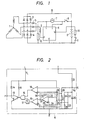
- FIG. 1 is a circuit diagram of the voltage regulator for a charging generator in accordance with one embodiment of the present invention.
- the charging generator consists of Y-connected armature windings 1 and a field winding 2.
- the a.c. output of the armature windings 1 is converted to a d.c. by three-phase full-wave rectifiers 3, 4 and an auxiliary rectifier 5.
- the voltage regulator 6 controls the current flowing through the field winding 2 and regulates the output voltage of the generator.
- Power is also supplied from a battery 9 to the field winding 2 through a key switch 8 and a charge lamp 7. This circuit supplies the power to the field winding 2 until the output of the generator reaches a predetermined value. The power which is converted to the d.c.
- a load 10 is connected to the battery 9 via a switch 11.
- another load 12 such as an auto-choke, heater or the like is connected to a connecting wire that connects the charge lamp 7 to the cathode of the auxiliary rectifier 5.
- Figure 2 is a circuit diagram showing the internal circuit of the voltage regulator 6 shown in Figure 1.
- a Darlington-connection power transistor 13 is connected to the F terminal which is in turn connected to the field coil 2.
- a flywheel diode 14 is also connected to the F terminal. The other end of this diode is connected to the L terminal so that when the power transistor 13 is turned off, it circulates the current flowing through the field winding 2 and prevents the occurrence of a high voltage in the field winding 2.
- a resistor 15 is interposed between the L terminal and the base of the power transistor 13 and applies a base current to the power transistor 13.
- An AND circuit 16 is connected to the base of the power transistor 13.
- a constant voltage diode 20 is disposed between I and E terminals via a resistor 21.
- a series circuit of resistors 22 and 23 and a series circuit of resistors 24 and 25 are connected in parallel with one another to the constant voltage diode 20 so as to divide the voltage that is generated by the constant voltage diode 20.
- a series circuit of resistors 26 and 27 is connected between S and E terminals to divide the voltage at the S terminal.
- a series circuit of resistors 28 and 29 is also disposed between the L and E terminals to divide the voltage at the L terminal. The voltage at the S terminal and the divided voltage of the set voltage are applied to the comparator 18.
- the divided voltage formed by the resistors 22, 23 is applied to one of the input terminals of the comparator 19 and the output voltage of a differential amplifier 30 is applied to the other.
- the differential amplifier 30 includes an operational amplifier 31 and resistors 32 through 35.
- the divided voltage at the S terminal- is applied to one of the terminals of the differential amplifier 30 and the divided voltage at the L terminal, to the other.
- the circuit having the construction described above operates in the following manner.
- an initial exciting current flows from the battery through the charge lamp 7, the field winding 2 and the power transistor 13.
- the constant voltage diode 20 inside the voltage regulator 6 supplies a predetermined voltage and the voltage at the S terminal, which is connected to the positive terminal of the battery 9, is below the set voltage V (ordinarily about 14.7 V) that is given by the resistors 22 through 25. Accordingly, the comparator 18 is at the high level.
- the output of the differential amplifier 30 is at the low level. For this reason, the output of the comparator 19 is at the high level.
- the holding circuit 17 transmits the high level as such to the AND circuit 16, so that the output of the AND circuit 16 is at the high level and the power transistor 13 becomes conductive.
- the field current attenuates through the flywheel diode 14 and reduces the output voltage of the generator.
- the voltage at the S terminal drops and the output of the comparator 18 rises to the high level.
- the output voltage of the AND circuit 16 rises then to the high level and the power transistor 13 becomes conductive, thereby raising the voltage of the generator.
- the operations described above are repeated and the battery voltage is controlled to a predetermined voltage, that is, to the set voltage V S .
- the output of the AND circuit 16 changes to the low level, whereupon the power transistor 13 is turned off and the supply of the current to the field winding 2 is stopped.
- the current of the field winding 2 then attenuates. Accordingly, the generator stops power generation and prevents the output voltage from reaching a high voltage. Since the operation of the generator is stopped, on the other hand, the current flows from the battery 9 through the charge lamp 7 and the load 12 and the charge lamp 7 is lit to raise the alarm.
- Figure 3 is a diagram showing the relation between the voltage V L at the cathode of the auxiliary diode 5, that is, the voltage at the L terminal, and the time (t).
- Curve 3A represents the voltage change when the load 10 shown in Figure 1 is a heavy load and the switch 11 is abruptly opened.
- the voltage V L at the L terminal instantaneously rises from the reference voltage V ss to the maximum voltage V L1 because the field current can not change abruptly due to the flywheel diode 14.
- Curve 3B represents the voltage waveform when breakage of the wire takes place. It has been a customary practice to detect the voltage V L at the L terminal so that when the voltage V L exceeds a predetermined voltage V LO , the operation of the generator is stopped. If the predetermined voltage V Lo is below the maximum voltage V L1 described above, however, the generator operation will be also stopped when the heavy load is stopped. Accordingly, the predetermined voltage V L0 must be higher than the maximum voltage V L1 . In this case, the voltage V L at the L terminal is higher than the maximum voltage V L1 .
- Figure 4 is a diagram showing the change of the voltage V s at the S terminal connected to the positive terminal of the battery 9 with respect to time.
- curve 4A represents the waveform when the load is changed over from ON to OFF and curve 4B does the waveform when the connecting wire B connecting the output of the generator to the battery 9 is broken.
- Figure 5 shows the relation between the voltage difference (V L -V S ) of the voltage V L at the L terminal and the voltage V s at the S terminal and the time.
- the waveform 5A when the load is released is remarkably smaller than the waveform 5B when the connecting wire B is broken. Since the present invention detects the voltage difference between the voltage V L at the L terminal and the voltage V s at the S terminal as the abnormal voltage, it can accurately detect abnormality.
- FIG. 6 illustrates one example of the holding circuit showing in Figure 1.
- two NAND gates 41 and 42 constitute a flip-flop.
- the input terminal 43 is connected to the input of one (42) of the NAND gates and the output of the NAND gate 41 is connected to the output terminal 44.
- a resistor 46 and a capacitor 47 are interposed between the power terminal 45 and the ground and the junction between these resistor and capacitor is connected to the NAND gate 41.
- the power terminal 45 is connected to the I terminal shown in Figure 2. When the voltage at the power terminal 45 is at the low level, the output of the NAND gate 41 is at the high level and the output terminal is at the high level, too. After the key switch 8 is made, the time delay circuit consisting of the resistor 46 and the capacitor 47 resets the output terminal 44 to the high level.
- Figure 7 illustrates the voltage regulator in accordance with another embodiment of the present invention.
- like reference numerals are used to identify like constituents as in Figure 2.
- the foregoing embodiment detects whether or not the voltage difference between the voltage at the L terminal and the voltage at the S terminal exceeds the predetermined value, whereas this embodiment detects the ratio of the voltage at the L terminal to the voltage at the S terminal.
- the divided voltages of V s and V L at the S and L terminals are applied respectively to a comparator 50.
- the divided voltage of the voltage V L at the L terminal by the resistors 28, 29 and the divided voltage of V s at the S terminal by the resistors 26, 27 are applied to the comparator 50 shown in Figure 7, so that the comparator 50 detects the ratio VLNs of the voltage V L at the L terminal to the voltage V s at the S terminal and the output voltage of the comparator 50 drops to the low level under the following condition; where R 26 , R 27 , R 28 , R 29 represent the resistance values of the resistors 26 through 29, respectively.
- the comparator 50 When the comparator 50 reaches the low level, the low level is transmitted to the AND circuit 16 through the holding circuit 17 and the power transistor 13 is cut off. This state continues until the holding circuit 17 is reset. Accordingly, the generator stops the power generating operation and it becomes possible to prevent the output voltage from rising to the high voltage.
- the circuit construction can be more simplified than the embodiment shown in Figure 2 and disconnection of the connecting wires can be reliably detected and even at the initial state, in the same way as the foregoing embodiment. Hence, it becomes possible to prevent the high voltage from being impressed upon the load and the voltage regulator.
- the current flows from the battery to the load 12 through the charge lamp and lights the charge lamp when the generator stops the power generating operation, but it is also possible to employ such a circuit construction in which a new circuit becomes conductive from the battery through the charge lamp when the voltage at the L terminal becomes the high voltage in order to raise the alarm of abnormality.
Landscapes
- Engineering & Computer Science (AREA)
- Power Engineering (AREA)
- Control Of Charge By Means Of Generators (AREA)
- Control Of Eletrric Generators (AREA)
Description
- This invention relates to a voltage regulator of the kind referred to in the pre-characterizing portion of
claim 1. Such a voltage regulator is known from EP-A-0 053 103. - A voltage regulator for a charging generator regulates the output voltage of the generator for charging a battery and holds the battery voltage connected to the generator at a predetermined level. The voltage regulator compares the battery voltage with a reference voltage and regulates the voltage. In this case, if disconnection of connecting wires connecting the generator to the battery occurs, the power is not fed to the battery and hence, the battery voltage drops. Accordingly, the output voltage of the generator rises so as to raise the battery voltage. When the voltage of the generator becomes a high voltage, the load connected directly to the output of the generator undergoes breakage or is burnt out. To solve this problem, the regulator is constructed so that when the output voltage of the generator exceeds a predetermined voltage, the operation of the generator is stopped. This construction is known in the art from JP-A-157942/1980, for example. In the case where a heavy load is connected to the battery, the output voltage of the generator will rise if this heavy load is drastically released. Accordingly, the voltage which stops the generation of the generator must be set to a voltage higher than the voltage which rises when the load is released, unless otherwise the operation of the generator will be stopped undesirably whenever the heavy load is released. However, if the voltage for stopping the generator operation is set to a high level, an undesirably high voltage will be impressed upon the load.
- EP-A-0 053 103 discloses a voltage regulator including a faults detecting and indicating circuit. In this circuit, reference signals V1 and V2 are. generated by a reference signal generator and a signal processor circuit generates a signal V, depending on the mean level of the output from the generator. The output signal of the signal processor circuit is compared to the reference signals V1 and V2. Namely, a comparator provides an output control signal when the test signal V, overruns the range defined by these reference signals V, and V2, so as to initiate an alarm indicator, i.e. indicating the faults in the generator.
- A detection as to whether the disconnection of the battery terminal or a change in the load is responsible for the changing of the battery voltage cannot be carried out with this voltage regulator having a faults detecting circuit.
- The present invention is therefore directed to provide a voltage regulator for a charging generator which is devoid of the problems described above. The object of the present invention is to provide a voltage regulator with a simple circuit construction for a charging generator which accurately detects the disconnection of connecting wires connecting the rectified output from the generator to the battery and does not apply any damage to the load.
- According to the invention this object is achieved by a voltage regulator of the kind referred to in the precharacterizing portion of
patent claim 1 comprising the features disclosed in the characterizing portion ofclaim 1. - The voltage regulator for a charging generator in accordance with the present invention is based upon the technical concept that when the connecting wires connecting the rectified output from the generator to the battery are disconnected or broken, the output voltage of the generator is different from the battery voltage but there is no remarkable difference between the output voltage and the battery voltage when the heavy load is released. Thus, the voltage regulator of the invention detects abnormality by comparing the rectified output voltage with the battery voltage.
- This comparision can be easily accomplished by detecting the voltage difference or a voltage ratio.
- It is necessary to raise an alarm using a simple device when the abnormality is detected. In the present invention, a circuit construction is employed in which the operation of the generator is stopped at the time of trouble and a current flows from the battery through a charge lamp so that the charge lamp is lit to raise the alarm.
-
- Figure 1 is a circuit diagram of a voltage regulator for a charging generator in accordance with one embodiment of the present invention;
- Figure 2 is a circuit diagram of the internal circuit of the voltage regulator shown in Figure 1;
- Figure 3 is a waveform chart showing the voltage (Vd at the L terminal;
- Figure 4 is a waveform chart showing the voltage (Vs) at the S terminal;
- Figure 5 is a waveform chart showing the difference voltage (VL-Vs) between the voltage at the L terminal and that at the S terminal;
- Figure 6 is a circuit diagram showing the internal circuit of a holding circuit of Figure 2;
- Figure 7 is a circuit diagram of the voltage regulator in accordance with another embodiment of the present invention; and
- Figure 8 is a waveform chart showing the voltage ratio of the voltage at the L terminal to the voltage at the S terminal.
- Figure 1 is a circuit diagram of the voltage regulator for a charging generator in accordance with one embodiment of the present invention. The charging generator consists of Y-connected
armature windings 1 and a field winding 2. The a.c. output of thearmature windings 1 is converted to a d.c. by three-phase full-wave rectifiers 3, 4 and an auxiliary rectifier 5. Thevoltage regulator 6 controls the current flowing through the field winding 2 and regulates the output voltage of the generator. Power is also supplied from a battery 9 to the field winding 2 through a key switch 8 and acharge lamp 7. This circuit supplies the power to the field winding 2 until the output of the generator reaches a predetermined value. The power which is converted to the d.c. by the three-phase full-wave rectifiers 3, 4 is applied to the battery 9. Aload 10 is connected to the battery 9 via a switch 11. On the other hand, anotherload 12 such as an auto-choke, heater or the like is connected to a connecting wire that connects thecharge lamp 7 to the cathode of the auxiliary rectifier 5. - Figure 2 is a circuit diagram showing the internal circuit of the
voltage regulator 6 shown in Figure 1. A Darlington-connection power transistor 13 is connected to the F terminal which is in turn connected to thefield coil 2. Aflywheel diode 14 is also connected to the F terminal. The other end of this diode is connected to the L terminal so that when thepower transistor 13 is turned off, it circulates the current flowing through the field winding 2 and prevents the occurrence of a high voltage in the field winding 2. Aresistor 15 is interposed between the L terminal and the base of thepower transistor 13 and applies a base current to thepower transistor 13. AnAND circuit 16 is connected to the base of thepower transistor 13. One of the input terminals of theAND circuit 16 is connected to acomparator 18 with the other being connected to anothercomparator 19 via aholding circuit 17. A constant voltage diode 20 is disposed between I and E terminals via aresistor 21. A series circuit ofresistors 22 and 23 and a series circuit ofresistors 24 and 25 are connected in parallel with one another to the constant voltage diode 20 so as to divide the voltage that is generated by the constant voltage diode 20. A series circuit ofresistors resistors comparator 18. The divided voltage formed by theresistors 22, 23 is applied to one of the input terminals of thecomparator 19 and the output voltage of adifferential amplifier 30 is applied to the other. Thedifferential amplifier 30 includes anoperational amplifier 31 and resistors 32 through 35. The divided voltage at the S terminal- is applied to one of the terminals of thedifferential amplifier 30 and the divided voltage at the L terminal, to the other. - The circuit having the construction described above operates in the following manner. When the key switch 8 is actuated, an initial exciting current flows from the battery through the
charge lamp 7, the field winding 2 and thepower transistor 13. Under this state, the constant voltage diode 20 inside thevoltage regulator 6 supplies a predetermined voltage and the voltage at the S terminal, which is connected to the positive terminal of the battery 9, is below the set voltage V (ordinarily about 14.7 V) that is given by the resistors 22 through 25. Accordingly, thecomparator 18 is at the high level. - Since the voltages at the L and S terminals as the input of the
differential amplifier 30 are substantially the same, the output of thedifferential amplifier 30 is at the low level. For this reason, the output of thecomparator 19 is at the high level. When the comparator output is at the high level, the holdingcircuit 17 transmits the high level as such to the ANDcircuit 16, so that the output of the ANDcircuit 16 is at the high level and thepower transistor 13 becomes conductive. - Next, when the generator starts generation, the voltage of the battery 9 rises and the current to the field winding 2 is supplied from the
armature windings 1 through the auxiliary rectifier 5. Accordingly, the current does not flow from the battery 9 to the field winding 2 any longer and the charge lamp is turned off. When the voltage of the battery 9 exceeds the set voltage VS, the output of thecomparator 18 drops to the low level and the output of the ANDcircuit 16 drops also to the low level. Hence, thepower transistor 13 becomes non-conductive. - The field current attenuates through the
flywheel diode 14 and reduces the output voltage of the generator. When the output voltage of the generator drops and the voltage of the battery 9 also drops, the voltage at the S terminal drops and the output of thecomparator 18 rises to the high level. The output voltage of the ANDcircuit 16 rises then to the high level and thepower transistor 13 becomes conductive, thereby raising the voltage of the generator. The operations described above are repeated and the battery voltage is controlled to a predetermined voltage, that is, to the set voltage VS. - Next, the protective operation when the connecting wires between the generator and the battery 9 are disconnected or broken will be explained.
- When the point B of the wire in Figure 1 is broken, for example, the battery 9 is not charged so that the voltage at the S terminal is low, the output of the
comparator 18 is always at the high level, thepower transistor 13 remains conductive, the output voltage of the generator becomes higher, the current flowing through the field winding 2 increases and the output voltage becomes all the more higher, thus establishing the non-control state. However, since the voltage difference between the voltage at the L terminal as the output terminal of the generator and the voltage at the S terminal as the voltage of the battery 9 is detected by thedifferential amplifier 30, the output voltage of thedifferential amplifier 30 becomes greater. When it exceeds the predetermined voltage, the output of thecomparator 19 drops to the low level. The holdingcircuit 17 holds this low level until it is reset. Accordingly, the output of the ANDcircuit 16 changes to the low level, whereupon thepower transistor 13 is turned off and the supply of the current to the field winding 2 is stopped. The current of the field winding 2 then attenuates. Accordingly, the generator stops power generation and prevents the output voltage from reaching a high voltage. Since the operation of the generator is stopped, on the other hand, the current flows from the battery 9 through thecharge lamp 7 and theload 12 and thecharge lamp 7 is lit to raise the alarm. - The advantages brought forth by the construction described above will be explained with reference to Figures 3, 4 and 5.
- Figure 3 is a diagram showing the relation between the voltage VL at the cathode of the auxiliary diode 5, that is, the voltage at the L terminal, and the time (t).
Curve 3A represents the voltage change when theload 10 shown in Figure 1 is a heavy load and the switch 11 is abruptly opened. The voltage VL at the L terminal instantaneously rises from the reference voltage Vss to the maximum voltage VL1 because the field current can not change abruptly due to theflywheel diode 14. -
Curve 3B represents the voltage waveform when breakage of the wire takes place. It has been a customary practice to detect the voltage VL at the L terminal so that when the voltage VL exceeds a predetermined voltage VLO, the operation of the generator is stopped. If the predetermined voltage VLo is below the maximum voltage VL1 described above, however, the generator operation will be also stopped when the heavy load is stopped. Accordingly, the predetermined voltage VL0 must be higher than the maximum voltage VL1. In this case, the voltage VL at the L terminal is higher than the maximum voltage VL1. - Figure 4 is a diagram showing the change of the voltage Vs at the S terminal connected to the positive terminal of the battery 9 with respect to time. In the diagram,
curve 4A represents the waveform when the load is changed over from ON to OFF andcurve 4B does the waveform when the connecting wire B connecting the output of the generator to the battery 9 is broken. Figure 5 shows the relation between the voltage difference (VL-VS) of the voltage VL at the L terminal and the voltage Vs at the S terminal and the time. Thewaveform 5A when the load is released is remarkably smaller than thewaveform 5B when the connecting wire B is broken. Since the present invention detects the voltage difference between the voltage VL at the L terminal and the voltage Vs at the S terminal as the abnormal voltage, it can accurately detect abnormality. - Figure 6 illustrates one example of the holding circuit showing in Figure 1. In the drawing, two
NAND gates input terminal 43 is connected to the input of one (42) of the NAND gates and the output of theNAND gate 41 is connected to theoutput terminal 44. Aresistor 46 and acapacitor 47 are interposed between thepower terminal 45 and the ground and the junction between these resistor and capacitor is connected to theNAND gate 41. Thepower terminal 45 is connected to the I terminal shown in Figure 2. When the voltage at thepower terminal 45 is at the low level, the output of theNAND gate 41 is at the high level and the output terminal is at the high level, too. After the key switch 8 is made, the time delay circuit consisting of theresistor 46 and thecapacitor 47 resets theoutput terminal 44 to the high level. Next, when theinput terminal 43 drops to the low level, the flip-flop inverts and theoutput terminal 44 drops to the low level. This state is kept when theinput terminal 43 rises to the high level until the key switch 8 is turned off and the voltage at thepower terminal 45 drops to the low level. Accordingly, the operation as the holdingcircuit 17 shown in Figure 2 is satisfied. - Figure 7 illustrates the voltage regulator in accordance with another embodiment of the present invention. In the drawing, like reference numerals are used to identify like constituents as in Figure 2. The foregoing embodiment detects whether or not the voltage difference between the voltage at the L terminal and the voltage at the S terminal exceeds the predetermined value, whereas this embodiment detects the ratio of the voltage at the L terminal to the voltage at the S terminal. In the drawing, the divided voltages of Vs and VL at the S and L terminals are applied respectively to a
comparator 50. - In the construction described above, the voltage regulating. operation under the steady state is accomplished in the same way as in the embodiment shown in Figure 2 and hence, the explanation is omitted.
- The case where the connecting wire between the generator and the battery 9 shown in Figure 1 is broken will be explained with reference to Figure 8. The voltage VL and Vs at the L and S terminals are those shown in Figures 3 and 4, respectively, when the switch 11 of the
load 10 is abruptly changed from ON to OFF at the time t1, and remains substantially at 1; hence, no great change occurs. When the connecting wire B is broken, on the other hand, a great change occurs as represented by curve 88. - The divided voltage of the voltage VL at the L terminal by the
resistors resistors comparator 50 shown in Figure 7, so that thecomparator 50 detects the ratio VLNs of the voltage VL at the L terminal to the voltage Vs at the S terminal and the output voltage of thecomparator 50 drops to the low level under the following condition;
resistors 26 through 29, respectively. - When the
comparator 50 reaches the low level, the low level is transmitted to the ANDcircuit 16 through the holdingcircuit 17 and thepower transistor 13 is cut off. This state continues until the holdingcircuit 17 is reset. Accordingly, the generator stops the power generating operation and it becomes possible to prevent the output voltage from rising to the high voltage. - According to this embodiment, the circuit construction can be more simplified than the embodiment shown in Figure 2 and disconnection of the connecting wires can be reliably detected and even at the initial state, in the same way as the foregoing embodiment. Hence, it becomes possible to prevent the high voltage from being impressed upon the load and the voltage regulator.
- In the embodiments described above, the current flows from the battery to the
load 12 through the charge lamp and lights the charge lamp when the generator stops the power generating operation, but it is also possible to employ such a circuit construction in which a new circuit becomes conductive from the battery through the charge lamp when the voltage at the L terminal becomes the high voltage in order to raise the alarm of abnormality.
Claims (5)
characterized by
auxiliary rectification means (5) for converting the a.c. output of said a.c. generator to d.c., said abnormality detection means (30) comparing the output voltage (Vd of said auxiliary rectification means with the battery voltage (Vs) and delivering the result thereof when the difference between both voltages exceeds a predetermined value; and by current cut-off means (13-17) for controlling said voltage regulator by means of the output of said abnormality detection means (30) and cutting off the current supplied to said field winding (2).
Applications Claiming Priority (2)
| Application Number | Priority Date | Filing Date | Title |
|---|---|---|---|
| JP19807/83 | 1983-02-10 | ||
| JP58019807A JPS59148538A (en) | 1983-02-10 | 1983-02-10 | Voltage regulator for charging generator |
Publications (2)
| Publication Number | Publication Date |
|---|---|
| EP0118779A1 EP0118779A1 (en) | 1984-09-19 |
| EP0118779B1 true EP0118779B1 (en) | 1987-11-11 |
Family
ID=12009601
Family Applications (1)
| Application Number | Title | Priority Date | Filing Date |
|---|---|---|---|
| EP84101384A Expired EP0118779B1 (en) | 1983-02-10 | 1984-02-10 | Voltage regulator for charging generator |
Country Status (5)
| Country | Link |
|---|---|
| US (1) | US4618811A (en) |
| EP (1) | EP0118779B1 (en) |
| JP (1) | JPS59148538A (en) |
| CA (1) | CA1209206A (en) |
| DE (1) | DE3467476D1 (en) |
Families Citing this family (20)
| Publication number | Priority date | Publication date | Assignee | Title |
|---|---|---|---|---|
| AU597900B2 (en) * | 1985-09-03 | 1990-06-14 | Robert Bosch (Australia) Proprietary Ltd. | Electronic voltage regulator circuit |
| JPH0545120Y2 (en) * | 1985-11-18 | 1993-11-17 | ||
| US4684818A (en) * | 1986-08-01 | 1987-08-04 | General Motors Corporation | Motor vehicle electrical system providing multiple DC voltages |
| JPH0349598A (en) * | 1989-07-13 | 1991-03-04 | Mitsubishi Electric Corp | Control apparatus of ac generator for vehicle |
| EP0430208B1 (en) * | 1989-11-29 | 1995-10-18 | Nippondenso Co., Ltd. | Charging control apparatus for vehicle generators |
| IT1240145B (en) * | 1990-03-22 | 1993-11-27 | Marelli Autronica | CHARGING SYSTEM OF THE BATTERY OF A MOTOR VEHICLE |
| DE4039404A1 (en) * | 1990-12-10 | 1992-06-11 | Sgs Thomson Microelectronics | OVERVOLTAGE PROTECTION DEVICE |
| US5294879A (en) * | 1991-11-01 | 1994-03-15 | Basler Electric Company | Microprocessor-controlled regulator |
| EP0709944A1 (en) * | 1994-10-31 | 1996-05-01 | STMicroelectronics S.r.l. | Charge voltage regulator for a battery |
| JP3531771B2 (en) * | 1994-12-28 | 2004-05-31 | 株式会社デンソー | Vehicle charging device |
| US6111390A (en) * | 1998-01-20 | 2000-08-29 | Kokusan Kenki Co., Ltd. | Magneto-equipped power device |
| DE19832874C2 (en) * | 1998-07-22 | 2000-10-26 | Daimler Chrysler Ag | Energy supply device for an electromagnetic valve control of an internal combustion engine |
| US6194877B1 (en) * | 1999-08-02 | 2001-02-27 | Visteon Global Technologies, Inc. | Fault detection in a motor vehicle charging system |
| JP4333022B2 (en) * | 2000-11-10 | 2009-09-16 | 株式会社デンソー | Power generation control system for vehicle generator |
| JP3520058B2 (en) * | 2001-06-11 | 2004-04-19 | 三菱電機株式会社 | Control device for vehicle generator |
| US6831445B2 (en) * | 2001-12-06 | 2004-12-14 | Denso Corporation | Automotive alternator having parallel connected circulating circuit to rapidly attenuate field current |
| JP3997969B2 (en) * | 2002-12-10 | 2007-10-24 | 株式会社デンソー | Power generation control device |
| US7173398B2 (en) * | 2003-10-10 | 2007-02-06 | Mitsubishi Denki Kabushiki Kaisha | System for controlling a vehicular generator |
| JP4395770B2 (en) | 2004-11-25 | 2010-01-13 | 株式会社デンソー | Method for detecting disconnection of charge line of battery charger and battery charger |
| JP4488056B2 (en) * | 2007-11-09 | 2010-06-23 | 株式会社デンソー | Vehicle power generation control device |
Family Cites Families (13)
| Publication number | Priority date | Publication date | Assignee | Title |
|---|---|---|---|---|
| DE2042529A1 (en) * | 1969-11-14 | 1971-05-19 | Nippon Denso Co | Voltage regulator for a generator that can be driven with rapidly changing speeds |
| US3656135A (en) * | 1970-04-29 | 1972-04-11 | Gen Motors Corp | Fault indicator circuit for vehicular battery charging systems |
| JPS5061612A (en) * | 1973-10-01 | 1975-05-27 | ||
| CA1013427A (en) * | 1973-10-22 | 1977-07-05 | Kazumasa Mori | Voltage regulating system |
| GB1494994A (en) * | 1973-12-08 | 1977-12-14 | Lucas Electrical Ltd | Battery charging systems for road vehicles |
| GB1494995A (en) * | 1973-12-08 | 1977-12-14 | Lucas Electrical Ltd | Battery charging systems for road vehicles |
| US3984755A (en) * | 1975-12-02 | 1976-10-05 | General Motors Corporation | Voltage regulator |
| FR2380656A1 (en) * | 1977-02-11 | 1978-09-08 | Sev Marchal | Voltage regulator system for battery charging generator - has visual warning of excessive or low charging rates using lamp and transistor with two threshold detecting stages |
| FR2416477A1 (en) * | 1978-02-02 | 1979-08-31 | Ducellier & Cie | FAULT DETECTION DEVICE BY INDICATOR LAMP FOR MOTOR VEHICLE ACCUMULATOR BATTERY CHARGING DEVICE |
| DE2843255A1 (en) * | 1978-10-04 | 1980-04-17 | Bosch Gmbh Robert | BATTERY CHARGING SYSTEM |
| US4306184A (en) * | 1979-05-04 | 1981-12-15 | Nippondenso Co., Ltd. | Generation control appparatus for vehicle generators |
| IT1130536B (en) * | 1980-11-26 | 1986-06-18 | Marelli Autronica | CIRCUIT FOR THE DETECTION AND SIGNALING OF FAULTS AND OPERATING ANOMALIES IN A RECHARGE SYSTEM FOR ELECTRIC ACCUMULATORS |
| JPS57177236A (en) * | 1981-04-20 | 1982-10-30 | Nippon Denso Co | Charger |
-
1983
- 1983-02-10 JP JP58019807A patent/JPS59148538A/en active Pending
-
1984
- 1984-02-06 CA CA000446865A patent/CA1209206A/en not_active Expired
- 1984-02-10 EP EP84101384A patent/EP0118779B1/en not_active Expired
- 1984-02-10 US US06/578,794 patent/US4618811A/en not_active Expired - Lifetime
- 1984-02-10 DE DE8484101384T patent/DE3467476D1/en not_active Expired
Also Published As
| Publication number | Publication date |
|---|---|
| US4618811A (en) | 1986-10-21 |
| EP0118779A1 (en) | 1984-09-19 |
| CA1209206A (en) | 1986-08-05 |
| JPS59148538A (en) | 1984-08-25 |
| DE3467476D1 (en) | 1987-12-17 |
Similar Documents
| Publication | Publication Date | Title |
|---|---|---|
| EP0118779B1 (en) | Voltage regulator for charging generator | |
| US4346341A (en) | Method and apparatus for automatic voltage reduction control | |
| US4578730A (en) | High-voltage DC circuit breaker apparatus | |
| EP0679898A2 (en) | Insulation state measurement method for decentralized power generating system | |
| CA2198273C (en) | An electronic trip device comprising a power supply device | |
| EP0408059B1 (en) | Vehicle AC generator control device | |
| EP0192832B1 (en) | Alternator system multifunction fault detector | |
| EP1306965B1 (en) | Power supply unit | |
| US4143313A (en) | Automotive voltage regulator to control voltge supply to an on-board vehicle network | |
| US4280161A (en) | Over-voltage protected, self-contained mobile electrical network system, particularly for automotive applications | |
| US5416401A (en) | Dual voltage supply circuit for vehicles | |
| US4658200A (en) | Protection circuit for voltage regulator of vehicle mounted generator | |
| US4342922A (en) | AC Fail-detect and battery switchover circuit for multi-bus power supply | |
| US6163138A (en) | Device for setting the output voltage in a three-phase alternator | |
| US4571533A (en) | Storage battery charging and monitoring apparatus | |
| US4755737A (en) | Control device for vehicle mounted generator | |
| US20020191361A1 (en) | Electronic trip device comprising a capacitor for supply of a trip coil | |
| US4471287A (en) | Charging generator control apparatus | |
| US5166594A (en) | Battery charging system with fault indication | |
| US4525662A (en) | Battery charging control system for automobile | |
| US4160282A (en) | Overcurrent protection apparatus | |
| US4672297A (en) | AC generator control status detecting device with short-circuit protection means | |
| US4222005A (en) | Testing device for generator output voltage regulators | |
| US4755734A (en) | Voltage regulator for vehicle mounted generator | |
| US4024456A (en) | Generator system with speed responsive output winding switching device |
Legal Events
| Date | Code | Title | Description |
|---|---|---|---|
| PUAI | Public reference made under article 153(3) epc to a published international application that has entered the european phase |
Free format text: ORIGINAL CODE: 0009012 |
|
| 17P | Request for examination filed |
Effective date: 19840214 |
|
| AK | Designated contracting states |
Designated state(s): DE FR GB |
|
| RAP1 | Party data changed (applicant data changed or rights of an application transferred) |
Owner name: HITACHI AUTOMOTIVE ENGINEERING CO., LTD. Owner name: HITACHI, LTD. |
|
| RAP1 | Party data changed (applicant data changed or rights of an application transferred) |
Owner name: HITACHI AUTOMOTIVE ENGINEERING CO., LTD. Owner name: HITACHI, LTD. |
|
| 17Q | First examination report despatched |
Effective date: 19860523 |
|
| GRAA | (expected) grant |
Free format text: ORIGINAL CODE: 0009210 |
|
| AK | Designated contracting states |
Kind code of ref document: B1 Designated state(s): DE FR GB |
|
| REF | Corresponds to: |
Ref document number: 3467476 Country of ref document: DE Date of ref document: 19871217 |
|
| ET | Fr: translation filed | ||
| PLBE | No opposition filed within time limit |
Free format text: ORIGINAL CODE: 0009261 |
|
| STAA | Information on the status of an ep patent application or granted ep patent |
Free format text: STATUS: NO OPPOSITION FILED WITHIN TIME LIMIT |
|
| 26N | No opposition filed | ||
| PGFP | Annual fee paid to national office [announced via postgrant information from national office to epo] |
Ref country code: GB Payment date: 20000124 Year of fee payment: 17 |
|
| PGFP | Annual fee paid to national office [announced via postgrant information from national office to epo] |
Ref country code: DE Payment date: 20000331 Year of fee payment: 17 |
|
| PG25 | Lapsed in a contracting state [announced via postgrant information from national office to epo] |
Ref country code: GB Free format text: LAPSE BECAUSE OF NON-PAYMENT OF DUE FEES Effective date: 20010210 |
|
| PGFP | Annual fee paid to national office [announced via postgrant information from national office to epo] |
Ref country code: FR Payment date: 20010215 Year of fee payment: 18 |
|
| GBPC | Gb: european patent ceased through non-payment of renewal fee |
Effective date: 20010210 |
|
| PG25 | Lapsed in a contracting state [announced via postgrant information from national office to epo] |
Ref country code: DE Free format text: LAPSE BECAUSE OF NON-PAYMENT OF DUE FEES Effective date: 20011201 |
|
| PG25 | Lapsed in a contracting state [announced via postgrant information from national office to epo] |
Ref country code: FR Free format text: LAPSE BECAUSE OF NON-PAYMENT OF DUE FEES Effective date: 20021031 |
|
| REG | Reference to a national code |
Ref country code: FR Ref legal event code: ST |