EP0116953A2 - Alignment apparatus - Google Patents
Alignment apparatus Download PDFInfo
- Publication number
- EP0116953A2 EP0116953A2 EP84101569A EP84101569A EP0116953A2 EP 0116953 A2 EP0116953 A2 EP 0116953A2 EP 84101569 A EP84101569 A EP 84101569A EP 84101569 A EP84101569 A EP 84101569A EP 0116953 A2 EP0116953 A2 EP 0116953A2
- Authority
- EP
- European Patent Office
- Prior art keywords
- mask
- wafer
- objective
- alignment
- prism
- Prior art date
- Legal status (The legal status is an assumption and is not a legal conclusion. Google has not performed a legal analysis and makes no representation as to the accuracy of the status listed.)
- Withdrawn
Links
Images


Classifications
-
- G—PHYSICS
- G03—PHOTOGRAPHY; CINEMATOGRAPHY; ANALOGOUS TECHNIQUES USING WAVES OTHER THAN OPTICAL WAVES; ELECTROGRAPHY; HOLOGRAPHY
- G03F—PHOTOMECHANICAL PRODUCTION OF TEXTURED OR PATTERNED SURFACES, e.g. FOR PRINTING, FOR PROCESSING OF SEMICONDUCTOR DEVICES; MATERIALS THEREFOR; ORIGINALS THEREFOR; APPARATUS SPECIALLY ADAPTED THEREFOR
- G03F9/00—Registration or positioning of originals, masks, frames, photographic sheets or textured or patterned surfaces, e.g. automatically
- G03F9/70—Registration or positioning of originals, masks, frames, photographic sheets or textured or patterned surfaces, e.g. automatically for microlithography
- G03F9/7003—Alignment type or strategy, e.g. leveling, global alignment
- G03F9/7023—Aligning or positioning in direction perpendicular to substrate surface
- G03F9/7026—Focusing
Definitions
- the present invention relates to an alignment apparatus in an X-ray aligner system etc., in which a mask and a wafer have their relative positions detected in a focused state and are aligned.
- a relative position detection apparatus including a dual focus optical system, for use in a proximity aligner system in which a wafer and a mask are exposed or gap to light with a minute clearance / therebetween has heretofore been known from Japanese Laid-open Patent Application No. 51-138464 or Japanese Laid-open Patent Application No. 52-126243.
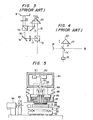
- Figure 1 shows a case where such known relative position detection apparatus is applied to the aligner system.
- Numeral 1 in Figure 1 designates a wafer, which is provided on its surface with a pattern 1 1 and three alignment marks 3 as shown in Figure 2(A).
- Numeral 2 in Figure 1 designates a mask, which is provided on its surface with a pattern surface 2' and three alignment marks 4 as shown in Figure 2(B).
- the alignment marks 3 of the wafer 1 and those 4 of the mask 2 are focused on a sensor 8 as will be described in detail later, whereby the relative positions of the wafer 1 and the mask 2 are detected with the images of both the alignment marks 3 and 4 superposed on the sensor 8 as shown in Figure 2(C).
- Illumination light emergent from a light source 10 is projected on the mask 2 and the wafer 1 via-an illuminating optical system 11, a semitransparent mirror 12, a mirror 13 and an objective 5.
- Light rays reflected from the wafer 1 and the mask 2 pass through the objective 5, mirror 13 and semitransparent mirror 12 again and reach a beam splitter 14, by which the light rays are split into a light path A15 and a light path B16.
- the light path A15 is a light path for focusing the alignment marks 4 on the mask 2 onto the sensor 8
- the light path B16 is a light path for focusing the alignment marks 3 on the wafer 1 onto the sensor 8.
- the light path B16 is provided with a magnification compensating lens 17 for equalizing the magnification of the alignment marks 3 on the wafer 1 to the magnification of the alignment marks 4 of the mask 2, and a mirror 18.
- the light path A15 which is the light path for focusing the alignment marks 4 on the mask 2 onto the sensor 8, is folded in order to focus the alignment marks 3 and 4 of the wafer 1 and the mask 2 on the sensor.
- the light beam passes through a prism 20 for compensating its optical length and further through a mirror 21, to reach a beam splitter 19.
- the light paths A15 and B16 are superposed by the beam splitter 19, and the real images of the alignment marks 3 and 4 of the mask 2 and the wafer 1 having the equal magnifications are formed at a first focusing point 22.
- the images are further passed through a relay lens 23 so as to be focused on the sensor 8.
- this relative position detection apparatus including the dual focus optical system is applied to a soft X-ray aligner system
- a positioning accuracy of within 0.1 ⁇ m is required.
- the circuit pattern on the mask can be printed on the wafer by enlarging or reducing it by changing the clearance between the wafer and the mask.
- the clearance between the wafer - thermal and the mask accordingly, the minute l expansion or contraction of the mask or wafer can be coped with, and the matching of patterns based on the joint use of the soft X-ray aligner system and a reduction projection aligner system (disclosed in U. S. Patent 4153371) can be established.
- Japanese Laid-open Patent Application No. 52-126243 discloses the use of a corner curb 20' as illustrated in Figure 4.
- symbol 14' denotes a semitransparent mirror
- symbols 18' and 21 1 denote reflectors.
- the expedient has the disadvantage that the corner curb 20' has three edges, which are observed and cannot be distinguished from the alignment marks of the mask and the wafer.
- Another disadvantage is that, since the semitransparent mirror 14 1 must be used, the quantities of light from the alignment marks of the mask and the wafer decrease to half, so the sensitivity lowers.
- the present invention has for its object to eliminate the disadvantages of the prior arts and to provide an alignment apparatus in an X-ray aligner system etc. in which focusing optical lengths are varied in accordance or gap with the clearance between a mask and a wafer, and the relative displacement magnitudes of the mask and the wafer are detected at high sensitivity and high accuracy in a focused state, whereby the mask and the wafer can be precisely aligned.
- the present invention for accomplishing the object is characterized, in an X-ray aligner system etc., in that at least one prism rectilinearly movable and in the shape of a right-angled triangle for changing optical lengths in accordance with the clearance between a mask and a wafer is disposed between an objective which serves to detect the images of the target marks of the mask and the wafer and a focusing position at which a photodetector is installed, light rays being reflected twice by each of the planes'of the prism which are slant by 45 degrees to the moving direction of the prism, whereby the target marks of the mask and the wafer are successively focused on the photodetector with their deviations relative to an optic axis prevented and at high sensitivity without decreasing the quantities of the light, and the mask and the wafer have the relative displacement magnitudes thereof detected so as to be aligned.
- the present invention is characterized in that the movement magnitude of the prism is measured, on the basis of which the displacement magnitude from the optic axis, of the alignment mark detected by the photodetector is subjected to a magnification-compensation., whereby the displacement magnitudes of the target mark of the mask and the alignment mark of the wafer are corrected to equal focusing magnifications.
- the present invention is also characterized in that, using a positioning jig in which a reflective layer such as aluminum evaporated film is formed on a substrate, a transparent layer such as polyimide film is formed on the reflective layer, and optical detection patterns are formed on the transparent layer, the optical detection patterns and the virtual images thereof formed on the reflective layer are detected, whereby the magnitude of an error attributed to the inclination of the optic axis of a microscope objective is precisely measured so as to compensate the displacement magnitudes of the respective target marks or to correct the inclination angle of the optic axis.
- the X-ray aligner system comprises an X-ray generator 84 which has an electron gun 81, a target 82, and a window 83 made of beryllium for taking out a soft X-ray beam 80 produced from the target 82; and a gastight chamber 85 which is connected with the X-ray generator 84.
- a Y-axial mask stage 87 which is supported - so as to be slidable in a Y-axial direction, by a base 86 constituting the gastight chamber 85 and which is driven by piezoelectric elements by way of example; and an X-axial mask stage 87' which is supported so as to be slidable in an X-axial direction by the Y-axial mask stage 87, which is driven by piezoelectric elements by way of example and whose lower end has a holding member 88 mounted thereon, this holding member serving to hold a mask 2 to be exposed to the X-rays.
- the base 86 can be vertically moved relative to the X-ray generator 84 so as to adjust the distance between the mask 2 and the target 82.
- a bellows 84' is provided to this end.
- the interior of the gastight chamber 85 is filled up with helium gas under a pressure substantially equal to the atmospheric pressure.
- the'X-ray aligner system comprises a wafer chuck 89 which holds by vacuum suction a wafer 1 opposing to the mask 2 with a gap of 10 ⁇ m - several tens ⁇ m therebetween, a vertical motion mechanism 90 which raises and lowers the whole wafer chuck 89 so as to adjust the gap between the mask 2 and the wafer 1, a 6 stage 91 to which the vertical motion mechanism 90 is attached and which is constructed so as to be rotatable within a horizontal plane, a Y-axial wafer table 92 which is constructed so as to move the ⁇ stage 91 in the Y-axial direction, and an X-axial wafer table 93 which is constructed so as to move the Y-axial wafer table 92 placed thereon, in the X-axial direction.
- Shown at numerals 94 and 95 are laser interferometers, which are disposed for measuring the position of the wafer 1' with reference to the mask 2 so as to expose the wafer 1 to the X-rays in step-and-repeat fashion.
- a circuit pattern to be printed becomes as fine as 1 ⁇ m or less. Therefore, it becomes necessary to match the circuit pattern to the minute expansion or contraction of the mask or wafer attributed to thermal expansion or contraction.
- the circuit pattern needs to be printed by jointly using the X-ray aligner system and a reduction projection aligner system.
- the matching is possible owing to the point source of the, radiation in the X-ray aligner system, in such a way that the general magnification at which the circuit pattern formed on the mask 2 is printed on the wafer 1 is enlarged or reduced by changing the gap between the mask 2 and the wafer 1.
- the relative position detection apparatus which can cope with the change of the gap between the mask 2 and the wafer 1 and which can align the mask and wafer at high precision is installed in the gastight chamber 85. Since the portion of a microscope objective in the relative position detection apparatus forms an obstacle in the exposure operation, it is constructed so as to be capable of advancing or retreating vertically and laterally. '
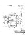
- Two prisms 42 and 46 are placed on and fixed to a carriage 48.
- the pair of rectangular prisms 42, 46 can move without changing their relative positions.
- An inverted prism 44 is fixed on the symmetrical line of the pair of rectangular prisms.
- Light rays respectively reflected from the wafer 1 and the mask 2 first enter the rectangular prism 42 through a semitransparent mirror 12, are reflected therein and exit therefrom; they have images reversed by the inverted prism 44 via a mirror 43; they enter the rectangular prism 46 through a mirror 45, are reflected therein and lastly exit therefrom; and they form real images at a first focusing point 22 via a mirror 47. Further, real images are formed on a sensor 8 by a relay lens 23 so as to perform position detection.
- the rectangular prism 42 and the rectangular prism 46 form light paths symmetric to each other.
- the light rays are reflected twice by these rectangular prisms 42 and 46, the first entrance and the last exit fall into a shifting relationship, and the light scarcely attenuates.
- the rectangular prisms 42, 46 are placed on the identical carriage 48, and this carriage 48 is reciprocated as indicated by arrow F, whereby optical lengths can be altered.
- the time-division dual detection is executed.
- the pair of rectangular prisms 42, 46 undergo rotations ⁇ 2 of equal magnitudes. Accordingly, optic axis deviations having developed in the rectangular prism 42 are reversed by the inverted prism 44 and then enter the rectangular prism 46, in which the optic axis deviations are canceled.
- Figure 7 is a light path diagram showing the arrangement of optical elements :.n the present embodiment.
- the rectangular prisms 42, 46 are fixed to the carriage 48, the carriage 48 and stationary members 50 are slidably supported by ball guides 49, and the carriage can be moved in the aforementioned slidable directions by a screw 51 and a driving motor 52.
- the screw 51 is mounted on the stationary members in rotatable fashion by a holder 53.
- the movement magnitude of the carriage 48 is detected by a sensor 27, and a magnification compensation is made by the use of the detected value. Then, the relative displacement magnitudes of the alignment mark of the mask and that of the wafer are detected, and the mask table or the wafer table is moved in the horizontal direction, thereby to positionally match the mask and the wafer.
- illumination light emitted from a light source 1.0 is projected on the mask 2 and the wafer 1 via an illuminating optical system 11, a semitransparent mirror 12, a mirror 13 and an objective 5.
- the light rays reflected from the wafer 1 and the mask 2 pass through the objective 5 and the mirror 13 again, are bent by the semitransparent mirror 12, are reflected by the rectangular prism 42 and the mirror 43, and reach the inverted prism 44. Further, the light rays emergent from the inverted prism 44 reach the mirror 45 and then the rectangular prism 46.
- the pair of rectangular prisms 42 and 46 are movable in the directions of the reciprocating arrow F.
- the light reflected by the rectangular prism 46 is reflected by the mirror 47, and forms the real image at the first focusing point 22. Further, the alignment marks 3 or the alignment marks 4 are imaged by the relay lens 23 on a photodetector 8 which is constructed of a self-scanned unidimensional linear image sensor such as a CCD.
- the image to be formed on the photodetector 8 concerns the distance from the rear principal point 7 of the objective 5 to the first focusing point 22 (refer also to Figures 10(A) and 10(B)).
- the alignment marks 3 of the wafer 1 are imaged when the rectangular prisms 42 and 46 are moved so as to establish an optical length b 1 .
- the alignment marks 4 of the mask 2 are imaged when the prisms 42 and 46 are moved so as to establish an optical length b 3 .
- the movement magnitude l 6 of the prisms 42 and 46 becomes (b 3 - b 1 )/4.
- the focused position of the rectangular prisms 42 and 46 at which the value of the function f becomes the maximum is detected by the sensor 27, and it is stored in a memory within the processing circuit 26.
- the focused position of the rectangular prisms 42 and 46 at which the value of the function f' becomes the maximum is detected by the sensor 27, and it is stored in the memory within the processing circuit 26.
- the central position of the alignment mark 3 on the wafer 1 is obtained from the digital signal V(N) detected in the focused state, by the technique of symmetry pattern matching as disclosed in, for example, U. S. Patent 4115762, whereupon the magnitude of displacement IA 1 between this central position and the optic axis is detected as shown in Figure 10(A).
- the central position of the alignment mark 4 on the mask 2 is obtained from the digital signal V'(N) detected in the focused state, by the technique of the symmetry pattern-matching as described above, whereupon the magnitude of displacement MA between this central position and the optic axis is detected as shown in Figure 10(B).
- the wafer 1 and the mask 2 have the gap therebetween, and are detected along the same light path. Therefore, the imaging magnification of the alignment mark 3 of the wafer 1 and the imaging magnification of the alignment mark 4 of the mask 2 are naturally unequal as shown in Figures 10(A) and 10(B).
- the coefficient K of the magnification compensation is given by the following equation (2): where b 1 becomes known when the displacement magnitude of the prisms 42 and 46 has been detected by the sensor 27, f denotes the focal distance of the objective 5 and is known, and 1 6 is obtained as described before.
- the mask and the wafer can be positionally matched.
- the reasons why the magnification must be compensated are that both the center of the alignment mark of the wafer and the center of the alignment mark of the mask do not always lie on the optic axis, and that the prisms 42 and 46 are moved in accordance with the gap formed between the mask and the wafer.
- the gap (a 1 - a 2 ) between the wafer 1 and the mask 2 can also be obtained by Equation (3) given below.
- Equation (3) the measurement of the gap may well be performed as described in U. S. Patent Application Serial No. 387206.
- the prisms 42 and 46 are moved in accordance with.the gap between the mask 2 and the wafer 1 so as to detect the respective alignment marks in the focused state, and the magnification compensation is made in aligning the mask and the wafer.
- the mask and the wafer can be accurately aligned even when the centers of the alignment marks deviate from the optic axis.
- the deviations of the optical images are eliminated against the inclination (a) and the lateral deviation (b) involved in moving the rectangular prisms 42 and 46, and the alignment apparatus is constructed of the reflecting optical system, so that the mask and the wafer can be aligned at high reliability without decreasing the quantity of light.
- Illumination light 56 from a light source 54 having passed through an optical fiber 55 is condensed by a condensing lens 57.
- a condensing lens 57 Via a mirror 58, a semitransparent prism 12 and a mirror 13, the light advances from a microscope objective 5 to a mask 2 along arrows indicated by broken lines in Figure 11. It passes through the mask 2 whose base is substantially transparent, and it is projected into the vicinity of an alignment mark on a wafer 1.
- Light rays reflected from the mask 2 and the wafer 1 pass through the microscope objective 5 again, and pass through the mirror 13 and the semitransparent prism 12 along arrows indicated by solid lines in Figure 11. They first enter a rectangular prism 20, are reflected therein and exit therefrom; they are shifted by a rectangular prism 60; and they pass through the rectangular prism 20 again while forming a light path symmetric to the previous light path. Owing to the light path formation, an imaging error correction based on the movement of the prism 20 is performed.
- the light having lastly exited from the rectangular prism 20 is reflected by a mirror 61, and is split into ' two light paths by a semitransparent prism 62.
- One light path split passes through a relay lens 23, and forms an image on a linear sensor 8.
- the other light path split passes through a relay lens 63 and forms an image on a TV imaging screen 64, the image being utilized for visual observation.
- the kind of the image to be formed depends upon the optical length from the microscope objective 5 to the linear sensor 8 or the TV imaging screen 64.
- the rectangular prism 20 is moved as indicated by arrow F, to change the optical length to any desired value and to form the image of the alignment mark of the mask 2 or the wafer 1 on the linear sensor 8, whereupon each position is detected.
- the embodiment shown in Figure 11 is such that the rectangular prisms 42 and 46 shown in Figure 7 are juxtaposed vertically and made unitary. Even when the corresponding rectangular prism 20 has inclined minutely in a direction (a) or has moved finely in a direction canceled and (b), the deviations of the optical image can be / prevented because the light ray is reflected twice by the upper and lower parts of the rectangular prism 20. Moreover, since the optical system is entirely reflective, decrease in the quantity of light is prevented and the alignment marks of both the mask and the wafer can be detected at high sensitivity, unlike the prior art illustrated in Figure 4.
- the rectangular prism 60 is held on a prism holder 25 which is turnably supported by a pin 24.
- the prism holder 25 can be finely turned and adjusted by a micrometer 26. Accordingly, the inclination of the rectangular prism 60 can be adjusted. .
- the rectangular prism 20 is similarly held on a prism holder 30 which is supported so as to be turnable about a pin 29 disposed on a carriage 48.
- This prism holder 30 can be finely turned and adjusted by a micrometer 31 which is disposed on the carriage 48. Accordingly, the inclination adjustment of the prism 20 is possible.
- Shown at numeral 32 is a wire, one end of which is fixed to the carriage 48 and the other end of which is wound on a pulley 33 attached to the output shaft of a motor 52.
- a sensor 27 serves to detect the displacement magnitude of the carriage 48, and is constructed of a differential transformer or the like.
- the alignment mark 4 of the mask 2 at a distance a 2 from the microscope objective 5 forms its image 66 at a distance b 3 from the microscope objective 5.
- the alignment mark 3 of the wafer 1 at a distance a 1 from the microscope objective 5 forms its image 67 at a distance b from the microscope objective 5.
- the alignment mark images 66 and 67 of the mask 2 and wafer 1 are respectively formed on the linear sensor 8 by changing the optical length through the movement of the prism 20 described above, whereupon the positions of the mask and wafer are detected.
- magnifications of the images formed on the linear sensor 8 are unequal.
- the relative positions of the mask 2 and wafer 1 are evaluated in such a way that the imaging magnification difference of the alignment mark images 66 and 67 of the mask 2 and wafer 1 is multiplied by the distance (L 1 ) from an optic axis 65 being an axis whose imaging position does not change even when the magnification has changed, to the place in which the'alignment mark image 67 of the wafer 1 is formed
- L 1 IA 1 .
- symbols 8a and 8b denote linear sensors.
- Figure 17 shows a positioning jig which serves as the reference of the relative positioning between the mask 1 and the wafer 2.
- the positioning jig for use in the present invention comprises a reflective layer 69 formed on a substrate 68 being a mirror wafer, a transparent layer 70 formed on the reflective layer 69, and optical detection patterns (hereinbelow, termed "detection patterns") 71 formed on the transparent layer 70.
- the reflective layer 69 is provided by depositing an aluminum evaporated film or the like.
- the transparent layer 70 is provided in such a way that a polyimide film or the like being a transparent member is stuck on the reflective layer 69 by spin coating.
- the thickness of the film by the spin coating is substantially determined by the viscosity of a coating agent and the spinning frequency thereof, and only about 0.8 - 1 ⁇ m can be applied by one coating. Therefore, the coating agent is dividedly applied several times. In general, the dispersion of film thicknesses due to the spin coating is about 0.01 ⁇ m, and it poses no problem even when the film is dividedly applied several times.
- the relationship between the thickness t of the transparent layer 70 and the gap g of the mask 2 and wafer 1 can be expressed by the following equation: where n ⁇ refractive index of the transparent layer (polyimide film).
- the gap g between the mask 2 and the wafer 1 is set at about 5 - 40 pm in view of the problem of blurring.
- the refractive index n of the polyimide film as the transparent layer 70 is about 1.5. In the case of the polyimide film, therefore, the thickness t of the transparent layer 70 is often made 3.75 - 40 ⁇ m in accordance with the calculation based on the above equation.
- the detection patterns 71 are provided on three places of the transparent layer 70, and the detection patterns 71 numbering three are arrayed in each of the places.
- the detection patterns 71 can be formed by substantially the same process as an LSI production process. Next, the dimensions of the detection patterns 71 will be described.
- the detection pattern 71 In order to detect the rear surface of the detection pattern 71 (the surface at which the detection pattern 71 lies in contact with the transparent layer 70) by the falling illumination with the microscope objective 5, it is required that, as illustrated in Figure 22, illumination light 72 from the microscope objective 5 be reflected by the reflective layer 69, and subsequently reflected by the detection pattern 71, whereupon reflected light 73 reflected again by the reflective layer 69 return to the microscope objective 5.
- the width w of the detection pattern 71 is too great, there arises the problem that the light once reflected by the rear surface of the detection pattern 71 returns to the rear surface of the detection pattern 71 again and does not return to the microscope objective 5, and hence, the detection pattern cannot be detected. Therefore, the width w of the detection pattern 71 and the spacing s between the adjacent detection patterns 71 must be set in appropriate ranges.
- the maximum value of the width w of the detection pattern 71 is determined by the thickness t and refractive index n of the polyimide film being the transparent layer 70 and the numerical aperture NA of the microscope objective 5 as illustrated in Figure 23, and it can be obtained by the following equation:
- the minimum spacing s-between the adjacent detection patterns 71 can be obtained by an equation similar to the equation for obtaining the maximum width w of the detection pattern 71:
- the detection is possible even when the spacing between the adjacent detection patterns 71 has a value smaller than the minimum spacing s obtained.
- the detection pattern 71_ is made of chromium oxide by way of example.
- the three detection patterns 71 in one place are arranged at a position where they can be detected once by the microscope objective 5 which is installed in a predetermined position.
- the detection patterns 71 of real images corresponding to the alignment marks 4 of the mask 2 and the detection patterns 71' of virtual images corresponding to the alignment marks 3 of the wafer 1 can be detected just in the state in which the mask 2 and the wafer 1 are relatively positioned ideally with the gap g therebetween.
- These detection values are error magnitudes which are incurred by the inclinations of the optic axes microscope 65 of the respective microscope objectives 5a and 5b.
- these deviation magnitudes ⁇ a and ⁇ b are compensated for the detected values of the respective alignment marks 4 and 3 by, e. g., calculation or a method of changing the inclination angles of the optic axes, whereby the relative positioning of high precision can be realized.
- symbols 8a and 8b denote linear sensors.
- the materials of the substrate 68, reflective layer 69 and transparent layer 70 of the positioning jig are not restricted to those in the embodiment, and the number of the detection patterns 71 is not restricted to that in the embodiment, either.
- an error magnitude ascribable to the inclination of the optic axis of a microscope objective is measured using a positioning jig wherein a reflective layer is formed on a substrate, a transparent layer is formed on the reflective layer, and detection patterns are formed on the transparent layer.
- the present invention can achieve the effect that the magnitude of relative displacement between the alignment mark of a mask and the alignment mark of a wafer can be accurately detected without decreasing the quantities of light from the alignment marks and in correspondence with the change of the gap between the mask and the wafer, so the mask and the wafer can be aligned at high precision.
Landscapes
- Physics & Mathematics (AREA)
- General Physics & Mathematics (AREA)
- Exposure Of Semiconductors, Excluding Electron Or Ion Beam Exposure (AREA)
- Exposure And Positioning Against Photoresist Photosensitive Materials (AREA)
Abstract
The present invention discloses, in an aligner system wherein a mask (2) and a wafer (1) are arranged so as to oppose to each other with a predetermined gap therebetween, an alignment apparatus comprising an objective which (5) focuses an alignment mark formed on the mask (2) and an alignment mark formed on the wafer (1); a photodetector (8) which images both the alignment marks; an optical length-varying optical system which includes at least one rectangular prism (20; 42, 46) that moves along a guide rectilinearly between said objective and the focusing position, to change an optical length and to bring each of the aligment marks into focus, light rays from the alignment marks entering said prism and existing therefrom even- numbered times so that the first entrance and the last exit may be shifted, the first entrance receiving optical images from said objective, the last exit being directed toward said photodetector (8); a displacement detecting sensor (27) which detects a magnitude of the movement of said rectangular prism (20; 42, 46) of said optical length-varying optical system; magnification compensation means (28) to compensate magnitudes of displacements of the respective alignment marks detected by said photodetector, from an optic axis by calculation based on the movement magnitude of said rectangular prism detected by said displacement detecting sensor (27), the optical length and a focal distance of said objective, so as to equalize magnifications of the images, and means (64) to detect a relative displacement. magnitude between the mask and the wafer by the use of the images of the equal magnifications compensated by said magnification compensation means, whereby the mask and the wafer can be aligned at high sensitivity and at high accuracy.
Description
- The present invention relates to an alignment apparatus in an X-ray aligner system etc., in which a mask and a wafer have their relative positions detected in a focused state and are aligned.
- A relative position detection apparatus including a dual focus optical system, for use in a proximity aligner system in which a wafer and a mask are exposed or gap to light with a minute clearance/therebetween, has heretofore been known from Japanese Laid-open Patent Application No. 51-138464 or Japanese Laid-open Patent Application No. 52-126243. Figure 1 shows a case where such known relative position detection apparatus is applied to the aligner system.
-
Numeral 1 in Figure 1 designates a wafer, which is provided on its surface with apattern 11 and threealignment marks 3 as shown in Figure 2(A). -
Numeral 2 in Figure 1 designates a mask, which is provided on its surface with a pattern surface 2' and threealignment marks 4 as shown in Figure 2(B). - In the dual focus detection method illustrated in Figure 1, the
alignment marks 3 of thewafer 1 and those 4 of themask 2 are focused on asensor 8 as will be described in detail later, whereby the relative positions of thewafer 1 and themask 2 are detected with the images of both thealignment marks sensor 8 as shown in Figure 2(C). Illumination light emergent from alight source 10 is projected on themask 2 and thewafer 1 via-an illuminatingoptical system 11, asemitransparent mirror 12, amirror 13 and an objective 5. Light rays reflected from thewafer 1 and themask 2 pass through the objective 5,mirror 13 andsemitransparent mirror 12 again and reach abeam splitter 14, by which the light rays are split into a light path A15 and a light path B16. - Here, the light path A15 is a light path for focusing the
alignment marks 4 on themask 2 onto thesensor 8, while the light path B16 is a light path for focusing thealignment marks 3 on thewafer 1 onto thesensor 8. - The light path B16 is provided with a
magnification compensating lens 17 for equalizing the magnification of thealignment marks 3 on thewafer 1 to the magnification of thealignment marks 4 of themask 2, and amirror 18. - The light path A15, which is the light path for focusing the
alignment marks 4 on themask 2 onto thesensor 8, is folded in order to focus thealignment marks wafer 1 and themask 2 on the sensor. The light beam passes through aprism 20 for compensating its optical length and further through amirror 21, to reach abeam splitter 19. - The light paths A15 and B16 are superposed by the
beam splitter 19, and the real images of thealignment marks mask 2 and thewafer 1 having the equal magnifications are formed at a first focusingpoint 22. - Herefrom, the images are further passed through a
relay lens 23 so as to be focused on thesensor 8. - Meanwhile, in a case where this relative position detection apparatus including the dual focus optical system is applied to a soft X-ray aligner system, a positioning accuracy of within 0.1 µm is required. On the other hand, since a soft X-ray source is close to a point source, the circuit pattern on the mask can be printed on the wafer by enlarging or reducing it by changing the clearance between the wafer and the mask. By adjusting the clearance between the wafer - thermal and the mask, accordingly, the minutelexpansion or contraction of the mask or wafer can be coped with, and the matching of patterns based on the joint use of the soft X-ray aligner system and a reduction projection aligner system (disclosed in U. S. Patent 4153371) can be established. However, when the clearance between the mask and the wafer is adjusted as described above by moving either the mask or the wafer, the alignment marks become out of focus in the light path A15 or B16 and need to be brought into focus by moving the
prism 20 etc. In a case where, in moving theprism 20 etc., thisprism 20 has deviated laterally or inclined as illustrated in Figure 3, the incident points of the light paths A15 and B16 on thesensor 8 disagree, resulting in the problem that the positioning accuracy mentioned above is not attainable. - As an expedient for solving this problem, Japanese Laid-open Patent Application No. 52-126243 discloses the use of a corner curb 20' as illustrated in Figure 4. Here, symbol 14' denotes a semitransparent mirror, and
symbols 18' and 211 denote reflectors. The expedient has the disadvantage that the corner curb 20' has three edges, which are observed and cannot be distinguished from the alignment marks of the mask and the wafer. Another disadvantage is that, since thesemitransparent mirror 141 must be used, the quantities of light from the alignment marks of the mask and the wafer decrease to half, so the sensitivity lowers. - The present invention has for its object to eliminate the disadvantages of the prior arts and to provide an alignment apparatus in an X-ray aligner system etc. in which focusing optical lengths are varied in accordance or gap with the clearance between a mask and a wafer, and the relative displacement magnitudes of the mask and the wafer are detected at high sensitivity and high accuracy in a focused state, whereby the mask and the wafer can be precisely aligned.
- The present invention for accomplishing the object is characterized, in an X-ray aligner system etc., in that at least one prism rectilinearly movable and in the shape of a right-angled triangle for changing optical lengths in accordance with the clearance between a mask and a wafer is disposed between an objective which serves to detect the images of the target marks of the mask and the wafer and a focusing position at which a photodetector is installed, light rays being reflected twice by each of the planes'of the prism which are slant by 45 degrees to the moving direction of the prism, whereby the target marks of the mask and the wafer are successively focused on the photodetector with their deviations relative to an optic axis prevented and at high sensitivity without decreasing the quantities of the light, and the mask and the wafer have the relative displacement magnitudes thereof detected so as to be aligned.
- Further, the present invention is characterized in that the movement magnitude of the prism is measured, on the basis of which the displacement magnitude from the optic axis, of the alignment mark detected by the photodetector is subjected to a magnification-compensation., whereby the displacement magnitudes of the target mark of the mask and the alignment mark of the wafer are corrected to equal focusing magnifications.
- The present invention is also characterized in that, using a positioning jig in which a reflective layer such as aluminum evaporated film is formed on a substrate, a transparent layer such as polyimide film is formed on the reflective layer, and optical detection patterns are formed on the transparent layer, the optical detection patterns and the virtual images thereof formed on the reflective layer are detected, whereby the magnitude of an error attributed to the inclination of the optic axis of a microscope objective is precisely measured so as to compensate the displacement magnitudes of the respective target marks or to correct the inclination angle of the optic axis.
-
- Figure 1 is a perspective view showing an example of a prior-art relative position detection apparatus;
- Figure 2(A) is a diagram showing an exposure region and alignment marks on a wafer, Figure 2(B) is'a diagram showing a circuit pattern and alignment marks formed on a mask, and Figure 2(c) is a diagram showing the state in which they are superposed;
- Figure 3 is a diagram for explaining the problem of an optical system shown in Figure 1;
- Figure 4 is a diagram showing the schematic setup of a prior-art relative position detection apparatus which has solved the problem illustrated in Figure 3;
- Figure 5 is a schematic setup diagram showing an X-ray aligner system which includes a relative position detection apparatus according to the present invention;
- Figures 6(A) and 6(B) are schematic arrangement diagrams showing an embodiment of the relative position detection apparatus according to the present invention, while Figure 7 is a diagram showing the embodiment in the concrete;
- Figure 8 is a diagram showing the schematic arrangement of a signal processor for alignment;
- Figure 9 is a diagram showing in correspondence with picture elements (N) an image signal waveform which is obtained from a photodetector constructed of a linear sensor;
- Figures 10(A) and 10(B) are diagrams for explaining magnification compensations;
- Figure 11 is a diagram showing another embodiment of the relative position detection apparatus different from the embodiment of-Figures 6(A) and 6(B) and 7;
- Figure 12 is a diagram showing the principle of relative position'detection;
- Figure 13 is an enlarged diagram of a part III in Figure 12;
- Figures 14 and 15 are diagrams showing relative position detections in the cases where the optic axes of microscope objectives are straight and slant, respectively;
- Figure 16 is an enlarged diagram of a part VI in Figure 15; and
- Figures 17 to 23 are diagrams for explaining a method according to the present invention for measuring the magnitude of an error attributed to the inclination of the optic axis of a microscope objective; wherein Figure 17 is a perspective view showing a positioning jig, Figure 18 is an enlarged vertical sectional view taken along line VIII - VIII in Figure 17, Figures 19 and 20 are diagrams showing the states in which relative positions are detected with the positioning jig as to respective cases where the optic axes of microscope objectives are straight and slant, Figure 21 is a partial enlarged diagram of the detection state, and Figures 22 and 23 are diagrams for explaining the operation of setting the width and interval of the detection patterns of the positioning jig.
- An X-ray aligner system which includes a relative position detection apparatus according to the present invention will be described with reference to Figure 5.
- The X-ray aligner system comprises an
X-ray generator 84 which has anelectron gun 81, atarget 82, and awindow 83 made of beryllium for taking out asoft X-ray beam 80 produced from thetarget 82; and agastight chamber 85 which is connected with theX-ray generator 84. At the lower end of thegastight chamber 85, there are disposed a Y-axial mask stage 87 which is supported - so as to be slidable in a Y-axial direction, by abase 86 constituting thegastight chamber 85 and which is driven by piezoelectric elements by way of example; and an X-axial mask stage 87' which is supported so as to be slidable in an X-axial direction by the Y-axial mask stage 87, which is driven by piezoelectric elements by way of example and whose lower end has aholding member 88 mounted thereon, this holding member serving to hold amask 2 to be exposed to the X-rays. Thebase 86 can be vertically moved relative to theX-ray generator 84 so as to adjust the distance between themask 2 and thetarget 82. A bellows 84' is provided to this end. In order to prevent the X-rays from attenuating, the interior of thegastight chamber 85 is filled up with helium gas under a pressure substantially equal to the atmospheric pressure. - Further, the'X-ray aligner system comprises a
wafer chuck 89 which holds by vacuum suction awafer 1 opposing to themask 2 with a gap of 10 µm - several tens µm therebetween, avertical motion mechanism 90 which raises and lowers thewhole wafer chuck 89 so as to adjust the gap between themask 2 and thewafer 1, a 6stage 91 to which thevertical motion mechanism 90 is attached and which is constructed so as to be rotatable within a horizontal plane, a Y-axial wafer table 92 which is constructed so as to move theθ stage 91 in the Y-axial direction, and an X-axial wafer table 93 which is constructed so as to move the Y-axial wafer table 92 placed thereon, in the X-axial direction. Shown atnumerals mask 2 so as to expose thewafer 1 to the X-rays in step-and-repeat fashion. In case of the X-ray aligner system, a circuit pattern to be printed becomes as fine as 1 µm or less. Therefore, it becomes necessary to match the circuit pattern to the minute expansion or contraction of the mask or wafer attributed to thermal expansion or contraction. In addition, the circuit pattern needs to be printed by jointly using the X-ray aligner system and a reduction projection aligner system. In either case, the matching is possible owing to the point source of the, radiation in the X-ray aligner system, in such a way that the general magnification at which the circuit pattern formed on themask 2 is printed on thewafer 1 is enlarged or reduced by changing the gap between themask 2 and thewafer 1. Besides, when the circuit pattern formed on themask 2 is printed on thewafer 1, they need to be positionally matched in the horizontal direction. To this end, the relative position detection apparatus which can cope with the change of the gap between themask 2 and thewafer 1 and which can align the mask and wafer at high precision is installed in thegastight chamber 85. Since the portion of a microscope objective in the relative position detection apparatus forms an obstacle in the exposure operation, it is constructed so as to be capable of advancing or retreating vertically and laterally.' - Next, the relative position detection apparatus according to the present invention will be concretely described with reference to Figures 6(A) and 6(B).
- Two
prisms carriage 48. Thus, the pair ofrectangular prisms inverted prism 44 is fixed on the symmetrical line of the pair of rectangular prisms. - Light rays respectively reflected from the
wafer 1 and themask 2 first enter therectangular prism 42 through asemitransparent mirror 12, are reflected therein and exit therefrom; they have images reversed by theinverted prism 44 via amirror 43; they enter therectangular prism 46 through amirror 45, are reflected therein and lastly exit therefrom; and they form real images at a first focusingpoint 22 via amirror 47. Further, real images are formed on asensor 8 by arelay lens 23 so as to perform position detection. - In this light path arrangement, owing to the provision of the
inverted prism 44, therectangular prism 42 and therectangular prism 46 form light paths symmetric to each other. The light rays are reflected twice by theserectangular prisms rectangular prisms identical carriage 48, and thiscarriage 48 is reciprocated as indicated by arrow F, whereby optical lengths can be altered. - With the above arrangement, the time-division dual detection is executed. In a case where the
carriage 48 inclines in the direction of arrow (a) as shown in Figure 6(A), the pair ofrectangular prisms rectangular prism 42 are reversed by theinverted prism 44 and then enter therectangular prism 46, in which the optic axis deviations are canceled. - In a case where the
carriage 48 deviates in the direction of arrow (b) as shown in Figure 6(B), therectangular prisms inverted prism 44. - As described above, even when the rotations in the direction of the arrow (a) or the lateral deviations in the direction of the arrow (b) have arisen in the case of changing the optical lengths by moving the carriage in the directions of the reciprocating arrow F, no optic axis deviation develops. Therefore, the relative positions of the mask and the wafer can be detected at high precision.
- Figure 7 is a light path diagram showing the arrangement of optical elements :.n the present embodiment. The
rectangular prisms carriage 48, thecarriage 48 andstationary members 50 are slidably supported by ball guides 49, and the carriage can be moved in the aforementioned slidable directions by ascrew 51 and a drivingmotor 52. - The
screw 51 is mounted on the stationary members in rotatable fashion by aholder 53. - The movement magnitude of the
carriage 48 is detected by asensor 27, and a magnification compensation is made by the use of the detected value. Then, the relative displacement magnitudes of the alignment mark of the mask and that of the wafer are detected, and the mask table or the wafer table is moved in the horizontal direction, thereby to positionally match the mask and the wafer. - More specifically, illumination light emitted from a light source 1.0 is projected on the
mask 2 and thewafer 1 via an illuminatingoptical system 11, asemitransparent mirror 12, amirror 13 and anobjective 5. - The light rays reflected from the
wafer 1 and themask 2 pass through theobjective 5 and themirror 13 again, are bent by thesemitransparent mirror 12, are reflected by therectangular prism 42 and themirror 43, and reach theinverted prism 44. Further, the light rays emergent from theinverted prism 44 reach themirror 45 and then therectangular prism 46. The pair ofrectangular prisms - The light reflected by the
rectangular prism 46 is reflected by themirror 47, and forms the real image at the first focusingpoint 22. Further, the alignment marks 3 or the alignment marks 4 are imaged by therelay lens 23 on aphotodetector 8 which is constructed of a self-scanned unidimensional linear image sensor such as a CCD. - The image to be formed on the
photodetector 8 concerns the distance from the rearprincipal point 7 of theobjective 5 to the first focusing point 22 (refer also to Figures 10(A) and 10(B)). In a case where thewafer 1 is at a distance a1 from the foreprincipal point 6 of theobjective 5, the alignment marks 3 of thewafer 1 are imaged when therectangular prisms mask 2 is at a distance a2 from the foreprincipal point 6 of theobjective 5, the alignment marks 4 of themask 2 are imaged when theprisms - In order to image the respective alignment marks on the
photodetector 8 in this manner, the movement magnitude ℓ6 of theprisms - First while the
rectangular prisms wafer 1 are imaged by the unidimensionallinear image sensor 8. Aprocessing circuit 26 shown in Figure 8 performs the A/D (analog-to-digital) conversion of image signals obtained from respective picture elements (N) as shown in Figure 9, and executes the calculation of 100 f =
rectangular prisms sensor 27, and it is stored in a memory within theprocessing circuit 26. Next, while theprisms mask 2 are imaged by the unidimensionallinear image sensor 8. Likewise to the above, theprocessing circuit 26 shown in Figure 8 performs the A/D conversion of image signals obtained from respective picture elements (N) as shown in Figure 9, 100 and executes the calculation of f' =
rectangular prisms sensor 27, and it is stored in the memory within theprocessing circuit 26. On the other hand, the central position of thealignment mark 3 on thewafer 1 is obtained from the digital signal V(N) detected in the focused state, by the technique of symmetry pattern matching as disclosed in, for example, U. S. Patent 4115762, whereupon the magnitude of displacement IA1 between this central position and the optic axis is detected as shown in Figure 10(A). Besides, the central position of thealignment mark 4 on themask 2 is obtained from the digital signal V'(N) detected in the focused state, by the technique of the symmetry pattern-matching as described above, whereupon the magnitude of displacement MA between this central position and the optic axis is detected as shown in Figure 10(B). - The
wafer 1 and themask 2 have the gap therebetween, and are detected along the same light path. Therefore, the imaging magnification
alignment mark 3 of thewafer 1 and the imaging magnification
alignment mark 4 of themask 2 are naturally unequal as shown in Figures 10(A) and 10(B). - In order to match it to the imaging magnification . m2 of the
alignment mark 4 of themask 2, the displacement magnitude IA1 detected as described above is subjected to the magnification compensation in accordance with the following equation (1) by acomputer 28 shown in Figure 8, so as to calculate IA2:
- That is, the coefficient K of the magnification compensation is given by the following equation (2):

prisms sensor 27, f denotes the focal distance of theobjective 5 and is known, and 16 is obtained as described before. - When the table on which the mask is placed or the table on which the wafer is placed is moved so as to equalize the magnification compensated value IA2 and the displacement value MA in this way, the mask and the wafer can be positionally matched. The reasons why the magnification must be compensated are that both the center of the alignment mark of the wafer and the center of the alignment mark of the mask do not always lie on the optic axis, and that the
prisms - Since, as described above, f is known and b and ℓ6 are detected, the gap (a1 - a2) between the
wafer 1 and themask 2 can also be obtained by Equation (3) given below. In the case of the X-ray aligner system, it is to be understood that the measurement of the gap may well be performed as described in U. S. Patent Application Serial No. 387206.
- As described above, the
prisms mask 2 and thewafer 1 so as to detect the respective alignment marks in the focused state, and the magnification compensation is made in aligning the mask and the wafer. As a result, the mask and the wafer can be accurately aligned even when the centers of the alignment marks deviate from the optic axis. The deviations of the optical images are eliminated against the inclination (a) and the lateral deviation (b) involved in moving therectangular prisms - Besides the embodiment shown in Figures 6(A) and 6(B) and Figure 7,.-an embodiment illustrated in Figures 11 to 14 can achieve similar functional effects. In this embodiment, alignments in the directions of X-, Y- and e-axes are performed by defecting
optical systems optical systems - Illumination light 56 from a
light source 54 having passed through anoptical fiber 55 is condensed by a condensinglens 57. Via amirror 58, asemitransparent prism 12 and amirror 13, the light advances from amicroscope objective 5 to amask 2 along arrows indicated by broken lines in Figure 11. It passes through themask 2 whose base is substantially transparent, and it is projected into the vicinity of an alignment mark on awafer 1. - Light rays reflected from the
mask 2 and thewafer 1 pass through themicroscope objective 5 again, and pass through themirror 13 and thesemitransparent prism 12 along arrows indicated by solid lines in Figure 11. They first enter arectangular prism 20, are reflected therein and exit therefrom; they are shifted by arectangular prism 60; and they pass through therectangular prism 20 again while forming a light path symmetric to the previous light path. Owing to the light path formation, an imaging error correction based on the movement of theprism 20 is performed. - The light having lastly exited from the
rectangular prism 20 is reflected by amirror 61, and is split into 'two light paths by asemitransparent prism 62. - One light path split passes through a
relay lens 23, and forms an image on alinear sensor 8. - The other light path split passes through a
relay lens 63 and forms an image on aTV imaging screen 64, the image being utilized for visual observation. - The kind of the image to be formed depends upon the optical length from the
microscope objective 5 to thelinear sensor 8 or theTV imaging screen 64. - Therefore, the
rectangular prism 20 is moved as indicated by arrow F, to change the optical length to any desired value and to form the image of the alignment mark of themask 2 or thewafer 1 on thelinear sensor 8, whereupon each position is detected. - The embodiment shown in Figure 11 is such that the
rectangular prisms rectangular prism 20 has inclined minutely in a direction (a) or has moved finely in a direction canceled and (b), the deviations of the optical image can be/prevented because the light ray is reflected twice by the upper and lower parts of therectangular prism 20. Moreover, since the optical system is entirely reflective, decrease in the quantity of light is prevented and the alignment marks of both the mask and the wafer can be detected at high sensitivity, unlike the prior art illustrated in Figure 4. Therectangular prism 60 is held on aprism holder 25 which is turnably supported by apin 24. Theprism holder 25 can be finely turned and adjusted by amicrometer 26. Accordingly, the inclination of therectangular prism 60 can be adjusted. . Therectangular prism 20 is similarly held on aprism holder 30 which is supported so as to be turnable about apin 29 disposed on acarriage 48. Thisprism holder 30 can be finely turned and adjusted by amicrometer 31 which is disposed on thecarriage 48. Accordingly, the inclination adjustment of theprism 20 is possible. Shown atnumeral 32 is a wire, one end of which is fixed to thecarriage 48 and the other end of which is wound on apulley 33 attached to the output shaft of amotor 52. Thus, thecarriage 48 can be moved in the F directions by driving themotor 52. Asensor 27 serves to detect the displacement magnitude of thecarriage 48, and is constructed of a differential transformer or the like. - Next, the principle of detecting the respective alignment marks will be described with reference to Figures 12 and 14.
- The
alignment mark 4 of themask 2 at a distance a2 from themicroscope objective 5 forms itsimage 66 at a distance b3 from themicroscope objective 5. In addition, thealignment mark 3 of thewafer 1 at a distance a1 from themicroscope objective 5 forms itsimage 67 at a distance b from themicroscope objective 5. Thealignment mark images mask 2 andwafer 1 are respectively formed on thelinear sensor 8 by changing the optical length through the movement of theprism 20 described above, whereupon the positions of the mask and wafer are detected. - According to the imaging law of optical lenses, however, the magnifications of the images formed on the
linear sensor 8 are unequal. - For this reason, the relative positions of the
mask 2 andwafer 1 are evaluated in such a way that the imaging magnification difference
alignment mark images mask 2 andwafer 1 is multiplied by the distance (L1) from anoptic axis 65 being an axis whose imaging position does not change even when the magnification has changed, to the place in whichthe'alignment mark image 67 of thewafer 1 is formed
- Originally, in the detection of the relative positions of the
mask 2 andwafer 1, it is clear that accurate relative positions cannot be found unless, as illustrated in Figure 14, themask 2 and thewafer 1 are arranged in parallel so that theoptic axes 65 ofmicroscope objectives mask 2 and thewafer 1. - In actuality, however, it is difficult to accurately set the
optic axes 65 of the plurality ofmicroscope objectives mask 2 andwafer 1, it is the situation to use the objectives as inclined as shown in Figures 15 and 16. - At this time, detection errors o attributed to the
inclined microscope objectives 


- In Figure 15,
symbols - A method of accurately measuring the error magnitude attributed to the inclination of the optic axis of the
microscope objective 5 in this manner will be concretely described with reference to Figures 17 to 23. - Figure 17 shows a positioning jig which serves as the reference of the relative positioning between the
mask 1 and thewafer 2. - The positioning jig for use in the present invention comprises a
reflective layer 69 formed on asubstrate 68 being a mirror wafer, atransparent layer 70 formed on thereflective layer 69, and optical detection patterns (hereinbelow, termed "detection patterns") 71 formed on thetransparent layer 70. - The
reflective layer 69 is provided by depositing an aluminum evaporated film or the like. - The
transparent layer 70 is provided in such a way that a polyimide film or the like being a transparent member is stuck on thereflective layer 69 by spin coating. The thickness of the film by the spin coating is substantially determined by the viscosity of a coating agent and the spinning frequency thereof, and only about 0.8 - 1 µm can be applied by one coating. Therefore, the coating agent is dividedly applied several times. In general, the dispersion of film thicknesses due to the spin coating is about 0.01 µm, and it poses no problem even when the film is dividedly applied several times. The relationship between the thickness t of thetransparent layer 70 and the gap g of themask 2 andwafer 1 can be expressed by the following equation:
- In general, in the X-ray aligner system employing a point light source, the gap g between the
mask 2 and thewafer 1 is set at about 5 - 40 pm in view of the problem of blurring. In addition, the refractive index n of the polyimide film as thetransparent layer 70 is about 1.5. In the case of the polyimide film, therefore, the thickness t of thetransparent layer 70 is often made 3.75 - 40 µm in accordance with the calculation based on the above equation. - In this embodiment, as shown in Figure 17, the
detection patterns 71 are provided on three places of thetransparent layer 70, and thedetection patterns 71 numbering three are arrayed in each of the places. In addition, thedetection patterns 71 can be formed by substantially the same process as an LSI production process. Next, the dimensions of thedetection patterns 71 will be described. - In order to detect the rear surface of the detection pattern 71 (the surface at which the
detection pattern 71 lies in contact with the transparent layer 70) by the falling illumination with themicroscope objective 5, it is required that, as illustrated in Figure 22, illumination light 72 from themicroscope objective 5 be reflected by thereflective layer 69, and subsequently reflected by thedetection pattern 71, whereupon reflected light 73 reflected again by thereflective layer 69 return to themicroscope objective 5. However, when the width w of thedetection pattern 71 is too great, there arises the problem that the light once reflected by the rear surface of thedetection pattern 71 returns to the rear surface of thedetection pattern 71 again and does not return to themicroscope objective 5, and hence, the detection pattern cannot be detected. Therefore, the width w of thedetection pattern 71 and the spacing s between theadjacent detection patterns 71 must be set in appropriate ranges. - The maximum value of the width w of the
detection pattern 71 is determined by the thickness t and refractive index n of the polyimide film being thetransparent layer 70 and the numerical aperture NA of themicroscope objective 5 as illustrated in Figure 23, and it can be obtained by the following equation: -

- Besides, the minimum spacing s-between the
adjacent detection patterns 71 can be obtained by an equation similar to the equation for obtaining the maximum width w of the detection pattern 71:
- However, in a case where the width of the
detection pattern 71 is sufficiently small, the detection is possible even when the spacing between theadjacent detection patterns 71 has a value smaller than the minimum spacing s obtained. - Next, the reflection factor of the
detection pattern 71 will be described. - When the positioning jig for use in the present invention is detected by the falling illumination, almost all the
illumination light 72 is reflected by thereflective layer 69, to return to the microscope objective, so that an area inside the field of view becomes very bright. In order to bestow a contrast, accordingly, a pattern close to black having a small reflection factor is required as the detection pattern 71_. For this reason, thedetection pattern 71 is made of chromium oxide by way of example. - The three
detection patterns 71 in one place are arranged at a position where they can be detected once by themicroscope objective 5 which is installed in a predetermined position. - When the positioning jig is detected by the
microscope objectives detection patterns 71 of real images corresponding to the alignment marks 4 of themask 2 and the detection patterns 71' of virtual images corresponding to the alignment marks 3 of thewafer 1 can be detected just in the state in which themask 2 and thewafer 1 are relatively positioned ideally with the gap g therebetween. - At this time, as illustrated in Figure 20, it is possible to detect the magnitudes of deviations δa and δb between'the optic axis whose imaging position does not change even when the magnification (optical length) has changed, and the
optic axes 65 which connect thedetection patterns 71 of the real images and those 71' of the virtual images detected by the microscope objectives 5a and 5b. - These detection values are error magnitudes which are incurred by the inclinations of the
optic axes microscope 65 of therespective microscope objectives - In case of relatively positioning the
mask 2 and thewafer 1 actually after the detection of the deviation magnitudes δa and δb, these deviation magnitudes δa and δb are compensated for the detected values of therespective alignment marks - In Figures 19 and 20,
symbols - The materials of the
substrate 68,reflective layer 69 andtransparent layer 70 of the positioning jig are not restricted to those in the embodiment, and the number of thedetection patterns 71 is not restricted to that in the embodiment, either. - In this manner; according to the present embodiment; an error magnitude ascribable to the inclination of the optic axis of a microscope objective is measured using a positioning jig wherein a reflective layer is formed on a substrate, a transparent layer is formed on the reflective layer, and detection patterns are formed on the transparent layer. This brings forth the effect that the error magnitude can be accurately measured. Since compensations can be made in the actual positioning between two objects by grasping such error magnitudes, there is the derivative effect that relative positioning of high precision can be realized.
- As set forth above, the present invention can achieve the effect that the magnitude of relative displacement between the alignment mark of a mask and the alignment mark of a wafer can be accurately detected without decreasing the quantities of light from the alignment marks and in correspondence with the change of the gap between the mask and the wafer, so the mask and the wafer can be aligned at high precision.
Claims (7)
1. In an aligner system wherein a mask and a wafer are arranged so as to oppose to each other with a predetermined gap therebetween;
an alignment apparatus characterized by comprising:
an objective (5) which focuses an alignment mark formed on the mask (2) and an alignment mark formed on the wafer (1),
a photodetector (8) which images both the alignment marks,
an optical length-varying optical system which includes at least one rectangular prism (20; 42, 46) that moves along a guide rectilinearly between said objective (5) and the focusing position (22), to change an optical length and to bring each of the alignment marks into focus, light rays from the alignment marks entering said prism (2D; 42, 46) and exiting therefrom even- numbered times so that the first entrance and the last exit may be shifted, the first entrance receiving optical images from said objective, the last exit being directed toward said photodetector,
a displacement detecting sensor (27) which detects a magnitude of the movement of said rectangular prism of said optical length-varying optical system,
magnification compensation means (28) to compensate magnitudes of displacements of the respective alignment marks detected by said photodetector (8), from an optic axis by calculation based on the movement magnitude of said rectangular prism detected by said displacement detecting sensor (27), the optical length and a focal distance of said objective (5), so as to equalize magnifications of the images, and
means (64) to detect a relative displacement magnitude between the mask and the wafer by the use of the images of the equal magnifications compensated by said magnification compensation means,
the mask and the wafer being aligned by moving them.
2. An alignment apparatus according to Claim 1, wherein said optical length-varying optical system comprises a rectangular prism (20) which reflects the light rays on its two planes so as to shift intermediate exit and entrance from the first-mentioned rectangular prism.
3. An alignment apparatus according to Claim 1, wherein said alignment apparatus is an X-ray aligner system comprising a soft X-ray generator (80-84) which generates a soft X-ray, a gastight chamber (85) which is connected at its upper end to said X-ray generator and is provided at its lower end with a mask stage (86) for holding the mask and which is filled with a gas such as helium, and a wafer table (92) on which the wafer is placed so as to oppose to the mask, and wherein said objective, said photodetector, the optical length varying means and said displacement detecting sensor are disposed in said gastight chamber.
4. An alignment apparatus according to Claim 1, wherein a pair of rectangular prisms (42, 46) are juxtaposed in said optical length-varying optical system, and an inverted prism (44) is disposed therebetween for reflecting the light rays so as to shift intermediate entrance and exit.
5. An alignment apparatus according to Claim 1, wherein a jig (68-70) in which a reflective layer (69) is formed on a substrate (68), a transparent layer (70) is formed on said reflective layer and optical detection patterns (71) are formed on said transparent layer (70), is disposed on the mask side of said objective so as to detect an inclination angle of the optic axis of said objective.
6. An alignment apparatus according to Claim 3, wherein the wafer holder on which the wafer is placed is vertically moved, whereby the gap between the mask and the wafer can be changed.
" 7. An alignment apparatus according to Claim 1, wherein said photodetector (8) is a linear image sensor which is arrayed in at least one dimension.
Applications Claiming Priority (6)
| Application Number | Priority Date | Filing Date | Title |
|---|---|---|---|
| JP58024552A JPS59151114A (en) | 1983-02-18 | 1983-02-18 | Time divided double detection of focus |
| JP24552/83 | 1983-02-18 | ||
| JP58026154A JPS59152624A (en) | 1983-02-21 | 1983-02-21 | Method for detecting time-split double focus |
| JP26154/83 | 1983-02-21 | ||
| JP58094017A JPS59220604A (en) | 1983-05-30 | 1983-05-30 | Method for detecting position between two objects opposed each other with minute gap therebetween |
| JP94017/83 | 1983-05-30 |
Publications (1)
| Publication Number | Publication Date |
|---|---|
| EP0116953A2 true EP0116953A2 (en) | 1984-08-29 |
Family
ID=27284701
Family Applications (1)
| Application Number | Title | Priority Date | Filing Date |
|---|---|---|---|
| EP84101569A Withdrawn EP0116953A2 (en) | 1983-02-18 | 1984-02-16 | Alignment apparatus |
Country Status (2)
| Country | Link |
|---|---|
| US (1) | US4614431A (en) |
| EP (1) | EP0116953A2 (en) |
Cited By (1)
| Publication number | Priority date | Publication date | Assignee | Title |
|---|---|---|---|---|
| DE4010880C1 (en) * | 1990-04-04 | 1991-05-02 | Karl Suess Kg Praezisionsgeraete Fuer Wissenschaft Und Industrie - Gmbh & Co, 8046 Garching, De |
Families Citing this family (23)
| Publication number | Priority date | Publication date | Assignee | Title |
|---|---|---|---|---|
| US4708484A (en) * | 1984-10-24 | 1987-11-24 | Hitachi, Ltd. | Projection alignment method and apparatus |
| EP0568478A1 (en) * | 1992-04-29 | 1993-11-03 | International Business Machines Corporation | Darkfield alignment system using a confocal spatial filter |
| US5943089A (en) * | 1996-08-23 | 1999-08-24 | Speedline Technologies, Inc. | Method and apparatus for viewing an object and for viewing a device that acts upon the object |
| US6469779B2 (en) * | 1997-02-07 | 2002-10-22 | Arcturus Engineering, Inc. | Laser capture microdissection method and apparatus |
| US6495195B2 (en) | 1997-02-14 | 2002-12-17 | Arcturus Engineering, Inc. | Broadband absorbing film for laser capture microdissection |
| US7075640B2 (en) | 1997-10-01 | 2006-07-11 | Arcturus Bioscience, Inc. | Consumable for laser capture microdissection |
| US5985085A (en) * | 1997-10-01 | 1999-11-16 | Arcturus Engineering, Inc. | Method of manufacturing consumable for laser capture microdissection |
| US7473401B1 (en) | 1997-12-04 | 2009-01-06 | Mds Analytical Technologies (Us) Inc. | Fluidic extraction of microdissected samples |
| JP2000048374A (en) * | 1998-07-30 | 2000-02-18 | Matsushita Electric Ind Co Ltd | Disk recording and reproducing device |
| US6865743B2 (en) * | 1999-02-24 | 2005-03-08 | Matsushita Electric Industrial Co., Ltd. | Optical head and method of manufacturing the same |
| AU4812600A (en) | 1999-04-29 | 2000-11-17 | Arcturus Engineering, Inc. | Processing technology for lcm samples |
| US6364386B1 (en) * | 1999-10-27 | 2002-04-02 | Agilent Technologies, Inc. | Apparatus and method for handling an integrated circuit |
| AU2922701A (en) * | 1999-11-04 | 2001-05-14 | Arcturus Engineering, Inc. | Automated laser capture microdissection |
| JP3802309B2 (en) * | 2000-03-28 | 2006-07-26 | 株式会社アドテックエンジニアリング | Positioning apparatus and exposure apparatus in multilayer circuit board manufacture |
| US8722357B2 (en) | 2001-11-05 | 2014-05-13 | Life Technologies Corporation | Automated microdissection instrument |
| US10156501B2 (en) | 2001-11-05 | 2018-12-18 | Life Technologies Corporation | Automated microdissection instrument for determining a location of a laser beam projection on a worksurface area |
| WO2006031574A2 (en) | 2004-09-09 | 2006-03-23 | Arcturus Bioscience, Inc. | Laser microdissection apparatus and method |
| JP2008062568A (en) * | 2006-09-08 | 2008-03-21 | Seiko Epson Corp | Jig and unit for aligning liquid injection head |
| JP4288519B2 (en) * | 2006-09-13 | 2009-07-01 | セイコーエプソン株式会社 | Alignment apparatus and alignment method |
| NL2003084A1 (en) * | 2008-06-27 | 2009-12-29 | Asml Netherlands Bv | Correction method for non-uniform reticle heating in a lithographic apparatus. |
| US8164753B2 (en) * | 2009-06-05 | 2012-04-24 | Nanya Technology Corp. | Alignment mark arrangement and alignment mark structure |
| US9338363B1 (en) | 2014-11-06 | 2016-05-10 | General Electric Company | Method and system for magnification correction from multiple focus planes |
| DE102015116672A1 (en) | 2015-01-05 | 2016-07-07 | Krohne Ag | Flowmeter |
Family Cites Families (3)
| Publication number | Priority date | Publication date | Assignee | Title |
|---|---|---|---|---|
| US3775012A (en) * | 1971-07-07 | 1973-11-27 | El Ab As | Means for determining distance |
| JPS51138464A (en) * | 1975-05-26 | 1976-11-30 | Hitachi Ltd | Device for detecting relative position of plural articles |
| JPS5838765B2 (en) * | 1976-04-14 | 1983-08-25 | キヤノン株式会社 | multifocal microscope |
-
1984
- 1984-02-16 EP EP84101569A patent/EP0116953A2/en not_active Withdrawn
- 1984-02-16 US US06/580,709 patent/US4614431A/en not_active Expired - Fee Related
Cited By (3)
| Publication number | Priority date | Publication date | Assignee | Title |
|---|---|---|---|---|
| DE4010880C1 (en) * | 1990-04-04 | 1991-05-02 | Karl Suess Kg Praezisionsgeraete Fuer Wissenschaft Und Industrie - Gmbh & Co, 8046 Garching, De | |
| EP0450592A2 (en) * | 1990-04-04 | 1991-10-09 | Karl SÀ¼ss KG Präzisionsgeräte für Wissenschaft und Industrie - GmbH & Co. | Alignment system, particularly for X-ray or photolithography |
| EP0450592A3 (en) * | 1990-04-04 | 1992-05-13 | Karl Suess Kg Praezisionsgeraete Fuer Wissenschaft Und Industrie - Gmbh & Co. | Alignment system, particularly for x-ray or photolithography |
Also Published As
| Publication number | Publication date |
|---|---|
| US4614431A (en) | 1986-09-30 |
Similar Documents
| Publication | Publication Date | Title |
|---|---|---|
| US4614431A (en) | Alignment apparatus with optical length-varying optical system | |
| US6020964A (en) | Interferometer system and lithograph apparatus including an interferometer system | |
| EP0961954B1 (en) | Repetitively projecting a mask pattern using a time-saving height measurement | |
| US6297876B1 (en) | Lithographic projection apparatus with an alignment system for aligning substrate on mask | |
| JP3200874B2 (en) | Projection exposure equipment | |
| WO1999032848A1 (en) | Interferometer system with two wavelengths, and lithographic apparatus provided with such a system | |
| US4669867A (en) | Alignment and exposure apparatus | |
| JPS6227536B2 (en) | ||
| US6198527B1 (en) | Projection exposure apparatus and exposure method | |
| EP0231977A1 (en) | Optical imaging arrangement comprising an opto-electric focussing-error detection system | |
| JPH0581046B2 (en) | ||
| JP3279979B2 (en) | Wafer / mask position detection apparatus and deformation error detection method | |
| US6049372A (en) | Exposure apparatus | |
| USRE38113E1 (en) | Method of driving mask stage and method of mask alignment | |
| JP3203676B2 (en) | Projection exposure equipment | |
| JPS62150106A (en) | Apparatus for detecting position | |
| US4040746A (en) | Optical congruence comparator | |
| JP3209189B2 (en) | Exposure apparatus and method | |
| JP3209186B2 (en) | Exposure apparatus and method | |
| JP3352280B2 (en) | Projection exposure apparatus adjusting method and exposure method | |
| JPH10242037A (en) | Position detecting equipment and method which use oblique optical axis optical system | |
| JPH09289160A (en) | Aligner | |
| JP2513281B2 (en) | Alignment device | |
| JPH10209029A (en) | Exposure device provided with alignment system | |
| US4732484A (en) | Apparatus for measuring the dimensions of a minute object |
Legal Events
| Date | Code | Title | Description |
|---|---|---|---|
| PUAI | Public reference made under article 153(3) epc to a published international application that has entered the european phase |
Free format text: ORIGINAL CODE: 0009012 |
|
| 17P | Request for examination filed |
Effective date: 19840227 |
|
| AK | Designated contracting states |
Designated state(s): DE FR GB |
|
| STAA | Information on the status of an ep patent application or granted ep patent |
Free format text: STATUS: THE APPLICATION HAS BEEN WITHDRAWN |
|
| 18W | Application withdrawn |
Withdrawal date: 19870325 |
|
| RIN1 | Information on inventor provided before grant (corrected) |
Inventor name: KOMEYAMA, YOSHIHIRO |