EP0116098A1 - Peripheral controller for i/o subsystem using slow devices - Google Patents
Peripheral controller for i/o subsystem using slow devices Download PDFInfo
- Publication number
- EP0116098A1 EP0116098A1 EP82305387A EP82305387A EP0116098A1 EP 0116098 A1 EP0116098 A1 EP 0116098A1 EP 82305387 A EP82305387 A EP 82305387A EP 82305387 A EP82305387 A EP 82305387A EP 0116098 A1 EP0116098 A1 EP 0116098A1
- Authority
- EP
- European Patent Office
- Prior art keywords
- memory
- peripheral
- data
- register
- instruction
- Prior art date
- Legal status (The legal status is an assumption and is not a legal conclusion. Google has not performed a legal analysis and makes no representation as to the accuracy of the status listed.)
- Granted
Links
Images


Classifications
-
- G—PHYSICS
- G06—COMPUTING; CALCULATING OR COUNTING
- G06F—ELECTRIC DIGITAL DATA PROCESSING
- G06F13/00—Interconnection of, or transfer of information or other signals between, memories, input/output devices or central processing units
- G06F13/38—Information transfer, e.g. on bus
- G06F13/42—Bus transfer protocol, e.g. handshake; Synchronisation
- G06F13/4204—Bus transfer protocol, e.g. handshake; Synchronisation on a parallel bus
- G06F13/4234—Bus transfer protocol, e.g. handshake; Synchronisation on a parallel bus being a memory bus
- G06F13/4243—Bus transfer protocol, e.g. handshake; Synchronisation on a parallel bus being a memory bus with synchronous protocol
-
- G—PHYSICS
- G06—COMPUTING; CALCULATING OR COUNTING
- G06F—ELECTRIC DIGITAL DATA PROCESSING
- G06F13/00—Interconnection of, or transfer of information or other signals between, memories, input/output devices or central processing units
- G06F13/10—Program control for peripheral devices
- G06F13/12—Program control for peripheral devices using hardware independent of the central processor, e.g. channel or peripheral processor
- G06F13/124—Program control for peripheral devices using hardware independent of the central processor, e.g. channel or peripheral processor where hardware is a sequential transfer control unit, e.g. microprocessor, peripheral processor or state-machine
Definitions
- This invention relates to peripheral controllers used in I/O systems for controlling data transfer operations between a main host computer and a plurality of peripheral terminal units.
- Microprocessors and microprocessor systems will be seen to generally follow the architectural formulas and interrelationships which were established from general computer technology. However, microprocessors making use of large scale integrated techniques can be made into small packages with the use of integrated circuit chips and will generally follow the pattern of using a central processing unit, memory inptu-output circuits and various other control and support circuitry.
- microprocessors will generally use a program counter which is used to select some portion of memory to be addressed for retrieving program instruction codes to be executed.
- each peripheral-controller which was situated in a base module was burdened with many processor and control circuits for handling the specific requirements of each peripheral terminal unit_leading to a heavy burden of circuitry in each peripheral-controller.
- a universal or architecturally standard microprocessor was developed which would provide a multiplicity of processing functions for use in a peripheral-controller so that the peripheral-controller would only need a limited amount of application dependent logic and circuitry for handling the particular types of peripherals which it serviced.
- the universal processor or as it is called here, the "universal I/O state machine” could serve as a standard unit for all types of peripheral-controllers so that each of the peripheral- controlers would only need to have the minimum amount of circuitry and programs required for application to the particular peripherals in the network.
- This generalized and simplified type of microprocessor executes its operations very rapidly and is designed to handle individual bytes for operations with peripheral devices which are "byte” oriented and also can execute processing and transfer operations with complete words (a word here being two 8-bit bytes symbolized as AB) for use with peripheral terminals which are "word oriented” and which can accept or transmit full words.
- the universal microprocessor working in conjunction with the peripheral-oriented application dependent logic module permits the development of a generalized type of peripheral-controller which can handle a plurality of peripheral units instead of requiring a separate controller for each peripheral unit. Since the hardware and programming of the microprocessor remains standard and constant for each of the peripheral-controllers while the application dependent module is programmed to cater to a group of selected peripherals, it is thus possible to accomplish not only great versatility in data transfer and control features but also to provide great economies in circuitry and cost.
- peripheral-controller In digital systems where many instructions and control signals are required for the transfer of data to a variety of different types of peripheral units, generally a specifically tailored and designed peripheral-controller was provided.which is particularly suited to handle the data transfers to and from a single particular type of peripheral unit. It was found that by providing a uniform microprocessor for all types of peripheral-controllers which only varied in the type of application dependent logic programs required for specific types of peripheral devices, that great economies of space and cost could be realized. Thus, the combination of a universal microprocessor working in conjunction with an application dependent module could form a peripheral-controller to serve data transfer functions previously requiring a series of peripheral-controllers.
- the processor of the peripheral-controller of the present invention upon receipt of an I/O data transfer command from a host computer, will generate instructions and execute data transfer operations to/from peripheral terminals by use of an application dependent logic module which provides an external memory with instructions for peripheral terminal control and which has control logic which recognizes when slow devices are addressed.
- the control logic can then initiate a WAIT signal to said universal processor slow down and regulate the rate of data transfers to slow memory and slow peripheral terminals.
- a linear microsequencer circuit operates a decoder-controller in the microprocessor.
- the microsequencer includes a micro-instruction PROM which is sequentially stepped by a State Counter after being initiated by the "Clear" signal.
- the micro-instruction PROM also receives signals from an instruction register and flag registers.
- the micro-instruction PROM then provides Control Term signals for operation of the microprocessor system.
- FIG. 1 there is seen a system block diagram of a typical Burroughs host computer system, with central processing unit cabinet 100 having basically a series of main memory modules 101, a memory control module 102, a data processor module 103, working in cooperation with a host dependent port module 104.
- the host dependent port module provides a series of communication cables 105 designated as MLI or message level interfaces. These message level interfaces provide communication lines to a base module cabinet 106 (or a plurality of such cabinets) which are designated as the Universal Input/Output Base Module Cabinet.
- the base module cabinet is built to support a plurality of universal input/output (UIO) base modules 107. Each of these UIO base modules provides communication, control, and data transfer lines to specific types of peripheral devices.
- UIO universal input/output
- the host dependent port module can have message level interfaces to a plurality of UIO base module cabinets. And likewise, each UIO base module cabinet may have message level interface communication lines to other host systems 200 (main memory and processor) in addition to the first described host system of FIG. 1.
- a base module cabinet can support from one to four UIO base modules.
- each of the UIO base modules contained up to eight peripheral-controllers 108 known as "line control processors" and each of the line control processors were dedicated to data transfer and control with a particular type of peripheral device 109.
- This plurality of separate peripheral-controllers for each different peripheral has now been replaced with a single universal microprocessor and application dependent logic module which constitutes a single peripheral-controller for handling a plurality of peripheral terminals.
- LEM line expansion module
- the host system as represented by the central processing unit cabinet 100 can communicate with up to 64 peripheral controllers (line control processors) for each message level interface (MLI), if the base module is provided with the unit known as an LEM or line expansion module.
- peripheral controllers line control processors
- MMI message level interface
- the host system 100 can have eight message level interfaces (HLI) and can thus communicate with up to 512 peripheral controllers (line control processors).
- HHI message level interfaces
- peripheral controllers line control processors
- the peripheral controllers or line control processors 5 are controllers which are dedicated to data transfer and control between a peripheral terminal and the main host system or a plurality of host systems.
- LCP line control processors
- the 2-Card LCP The 2-Card LCP:
- This peripheral controller has a first card which is designated as the CF E or common front-end on which there are supplied a plurality of read-only memories (ROM's); hardware-wise these common front-end cards are of the same construction and nature except that in individual cases the ROMs are made to hold different programs which are suitable to the application at hand or the peripheral device with which it is used; thus, hardware-wise all the front-end cards will be found to be the same physically but only differ in the fact that different program material is inserted in the individual ROMs.
- the second card in the 2-card LC P is the PDC or peripheral dependent card. This card is uniquely built and adapted to suit the particular type of peripheral unit to which it communicates. It may be designated as an "application dependent logic module" .
- the first card is the CFE or common - 5 front-end card which is physically the same except for different programming, inside the ROM, this program being varied according to the application required.
- the second card is the CDC or common data card which is tailored to suit the requirements of different peripheral units; however, it 0 may be the same for such a group of items as magnetic tape, punched card-tape, disk pack, and console controls.
- the third card of the 3-card LCP is designated as the PDC or peripheral dependent card. This card is unique and is designed to handle one particular type of peripheral device.
- FIG. 4A there is seen a more detailed perspective drawing of a typical I/O base module 107.
- a plurality of these base modules are housed and serviced by a base module cabinet 126 of FIG. 1.
- the base module 107 provides housing whereby printed circuit cards holding integrated circuitry may be inserted on sliding tracks in order to connect with the backplane connectors for automatic connection into the system.
- a peripheral controller (or line control processor) 108 may require, as previously described, two printed circuit or three printed circuit cards.
- the base module may support up to eight such peripheral controllers in its housing. Communications between.the base module and the host system are controlled by distribution card 110.
- Other specialized handling printed circuit cards may be inserted, such as the previously mentioned line expansion module, common front-end card, common data card; or a second distribution control card, etc., can be inserted for connection into said base module 107.
- the frontplane or foreplane permits jumper cable connections 111 (FIG. 4A) between printed circuit cards and also permits connection cables such as message level interface 105 to the host computer or ribbon cable 109 c to permit connection from the base module to external devices such as peripheral device 109.
- An interface panel 106 may be provided on the base module cabinet 120 to provide for cable connectors such as 104 cc' 109 to facilitate disassembly and reconnection.
- each base module unit is provided with a Distribution Control Card 110, FIG. 4A, which connects the message level interface from the main host system to a selectively addressed line control processor (peripheral controller) in that base module.
- the base module has a common maintenance card and a common termination card which acts in common to service the entire group of up to eight line control processors in a base module.
- the UIO base module may also support a line expansion module or LEM. This feature expands the usage of a UIO base module by adding another Distribution Control Card which permits connection of that base module to yet another main host system in addition to the one already connected to the first Distribution Control Card. Thus, communication from a main host system can be expanded to cover two or more UIO base modules and their attendant line control processors. Likewise, two or more host systems can be made to communicate to a UIO base module or a plurality of such base modules.
- LEM line expansion module
- the base control card serves two basic functions; (a) to provide an interlock when multiple host computers try to access a base module, so that line control processors can thus be locked out from use by unauthorized host computers, and (b) to provide assorted features such as a base identification (ID) number and for maintenance control.
- the BCC is not mandatory when multiple hosts are connected to a base; however, it is useful.
- the base control card can also be used when only a single host computer is connected to the UIO base module.
- the BCC is an independent and optional module, as is the line expansion module LEM.
- the base module when a host computer is connected to a UIO base module, the base module must.have at least one distribution card 110, FIG. 4A, for each host computer which is connected to it.
- the base module when a UIO base module is connected to a multiple number of host computers, then there is need for the base module to be provided with a unit known as the PSM or path selection module.
- the path selection module is the control unit which regulates the communication to and from the multiple number of distribution cards in the U IO base module.
- UIO-SM universal input/output state machine
- the UIO state machine could be built typically on a 112 chip circuit board and be placed within the slide-in card rack which is supported by the LCP base module (now called UIO base module).
- the U IO state machine can interface easily to any application dependent logic through its front plane and, except for power connections and clock connections, no connections needed to be made to the LCP or UIO base backplane.
- the universal I/O state machine is basically implemented in transistor type logic (TTL).
- the UIO-SM has been made to implement a useful group of general purpose operators which include:
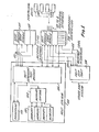
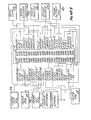
- FIG. 2 there is shown a schematic diagram,of a peripheral-controller for the I/O Subsystem of the present invention.
- the peripheral-controller is composed of a U IO State Machine 1 and an associated Application Dependent Logic Module 60 L which provides an external memory 90, control logic 66 and external registers 60 which connect to host system 10 and to peripheral 109 (via adapter 109 c ) ⁇
- the UIO State Machine 1 is seen to be provided with Instruction-Execution Logic 2, Memory Address Logic 3, Data Manipulation Logic 4, and an internal program memory 50.
- the Application Dependent Logic Module 60 L is connected by busses 10, 11, 12, 16 to the State Machine 1.
- the Logic Module 60 L provides an external memory 90 plus bus logic 66' and interface control logic 66 which includes an address decoder 66 ad for sensing addresses of "slow" elements, and an external register 60 which has bus connections to the Host System 10 and Peripheral Terminals such as 109.
- FIGS. 2A and 2B there is seen an overall block diagram of the UIO state machine.
- the input/output lines at the bottom of the drawing are all front plane lines which connect to the peripheral's application dependent control (PDC) logic since it is desired that the UIO state machine itself be independent of any application type logic or of the special requirements of particular peripheral units.
- PDC application dependent control
- FIGS. 2A and 2B there will be seen a series of interconnecting lines 16, 17 1 , 17 2' 18, 10, 19, 11, 12 and 20, which connect to the application dependent logic 60 L .
- These lines are labeled, such as the external memory data output bus 12, the I/O and memory write parity line 18, the memory address bus 16, the memory write enable 19 (and other functions listed on F I G. 2), the direct memory access (DMA) request line 11 (and other functions on FIG. 2), in addition to the main I/O bus 10.
- Line 15 is the instruction output bus from the program PROM 50.
- a program counter 41 having input lines from stack memory 45 and I/O bus 10, via 10 f' provides an output line which feeds an input signal to the program PROM 50 (internal memory 50).
- a memory reference register 40 receives its input signals via I/O bus 10 from accumulator registers 30, memory operand 31, and the save-MRR 47 (memory reference register-save).
- Repetition counter 42 also receives an input line via I/O bus 10 for signals from accumulator registers 30 and memory operand 31.
- the stack memory 45 controlled by stack pointer 46, provides an output line to the program counter 41.
- the repetition counter 42 provides an output which feeds back around line 10 f over to the I/O bus 10 and also around to the accumulator registers 30.
- Attached and receiving input from the I/O bus 10 is a control register 1 designated as item 37, a control register 2 designated as item 38 and a parity register 39.
- the control registers 37, 38 provide buffering of signals to application control register lines 17 1 , 17 2 .
- the parity generator 39 has 5 an output line 18 (part of I/O bus 10) and provides "I/O and memory write" parity.
- the memory output data bus 12 from RAM external memory 90 connects to the memory operand register 31 whose outputs feed to ALU 32 and parity check circuitry 21 which 0 has an output line 20 to provide memory read parity to external memory 90.
- Data bus 12 also provides an input to the instruction register 22 which has an output line connecting to the input of the instruction decoder-controller 23. Situated within instruction decoder-controller 23 are 5 external flag registers 23 e' interrupt mask 23 i' and state counter 23 s .
- Accumulator registers 30 actually comprise two sets of eight registers, one set designated 30 f (foreground accumulator registers) and the other set as 30 b (background). Each of the 16 registers are addressed and selected by an address line 23 a from the instruction decoder-controller 23.
- the I/O bus 10 provides a channel to the accumulator registers 30 which have an output to the B input of the arithmetic logic unit 32.
- Another input A to the arithmetic logic unit 32 comes from the memory operand register 31 which gets its input from external memory via the memory output bus 12, or from internal memory via bus 15.
- the arithmetic logic unit 32 has one set of outputs which feed to the "foreground” flag register 35 and another set of outputs to the "background” flag register 36. These flag registers 35 and 36 form an output which is fed to the instruction decoder-controller 23. They are used to signal "foreground mode” conditions for normal operation and "background mode” conditions for interrupts or emergency operation.
- the F output of the. arithmetic logic unit 32 feeds on a bus 10. to the shift logic circuitry 33 and to the byte-swap circuitry 34. The outputs of these circuits 33, 34 connect to the I/O bus 10.
- the PUT O P (operator) writes a 16-bit word (two bytes symbolized as A B) from the I/O bus 10 into a selected application dependent register 60 (external register), the particular register being addressed via GET-PUT address lines 19.
- the PUT OP can address any one of 32 application dependent registers.
- the GET OP reads a 16-bit word from a selected application dependent register 60 into an accumulator register 30 on the UIO-SM or into RAM memory 90 through the I/O bus 10.
- the GET OP can also address a selected one of the 32 application dependent registers 60 (external registers).
- the UIO-SM has the ability to repeat certain OP's (PUT's, GET's and logical OP's) by loading a number N (from the software) into a repetition counter 42 to control the memory reference register (MRR) 40 which is used as a counter after having been loaded with the starting address of the data block to be used in the "repeated" OP.
- OP's PUT's, GET's and logical OP's
- MRR memory reference register
- control registers 37, 38 In order to hold "PUT Data" for a longer period of time than can occur directly off of I/O bus 10, there are two 8-bit registers (control registers 37, 38) which have been placed in the UIO-SM. The strobing of these registers 37, 38 is under the control of the application dependent logic 60 L (FIG. 2).
- a "WAIT line” (on bus 11) has been built into the UIO-SM such that when an external "slow memory” is addressed, ; the “slow memory” can force the UIO-SM to wait however long required for the Read or the Write to be valid. This is seen on FIG. 2 at bus 11 which feeds signals to the instruction decoder-controller 23. This line can also be used to halt the machine.
- a clock enable line on bus 11 (CLKENB) has been included so that the application dependent logic 60 L may control the state machine clock for single pulse operations and also direct memory access (DMA) operations. The timing for this signal is the same as the WAIT signal on bus 11.
- the UIO-SM can check via circuitry 21 for odd parity on each memory fetch. All memory fetches from external memory 90 come on the memory output data bus which is shown as bus 12 and which connects to instruction register 22 and to the memory operand register 31. All memory writes go out on the I/O bus 10 along with odd parity on line 18.
- the UIO-SM contains 8-K words of user-defined instruction programs in PROM 50 which is capable of being expanded to 64-K words.
- memory addresses can come from two sources -- the program counter 41 and the memory reference register (MRR) 40.
- the UIO-SM provides the ability to do condition and unconditional Branches, Calls and Returns. "Calls" can be nested up to 16 levels from stack memory 45.
- the memory reference register 40 stores addresses and is used (at certain times specified in instruction words) to address RAM data memory 90 which will provide programs applicable to the peripheral device connecting to the application dependent logic module 60 L .
- This external memory 90 also serves to store data which is being transferred between the host computer and the peripheral terminal device.
- the memory reference register (MRR) 40 Since memory 90 and 50 are organized two bytes wide (16-bits plus parity) but the data for transfer is sometimes required in single byte form, as for peripherals such as card readers, the memory reference register (MRR) 40 has been designed such that only the high order 15-bits are used to address memory 90.
- the low order bit (BYTESWP) is used by the byte-oriented read/write OP's to determine whether or not to byte-swap the two byte data word before storage into accumulator registers 30 on an "external data memory read" or before storage into external RAM data memory 90 on a "data memory write".
- This particular feature permits the UIO-SM to easily handle byte-oriented data in that the desired byte is automatically read into the "low order" byte position of the accumulator registers 30 on “data memory reads”, as well as being automatically written from the "low order” byte position into the correct byte position on “data memory writes”.
- the "high order" byte position of the accumulator registers 30 must contain the last byte written, if any is present.
- the external memory output data bus 12, or internal memory instruction bus 15 provides 17 bits designated 0-16.
- the bus bits 0-7 (low order) constitute the "B" byte while the bus bits 8-15 constitute the "A" byte (high order).
- certain fields are specified such as the P field for odd parity, the basic function field Fl, F0, and function variant field by V4-VO.
- the destination specifier field is designated D3-D0; the source accumulator field is designated S2, Sl, S0.
- the field which causes selection of the memory address source to be used in fetching the operand of the instruction is designated M; while the function field for copying the arithmetic logic unit output into the memory reference register 40 is designated by the field C.
- the odd parity bit is set such that an odd number of 1's will exist across the entire 17-bit instruction (or the operand).
- the basic function field Fl, FO is described in Table II such that various binary digit combinations of Fl, FO provide certain functions as shown.
- the GET function provides for the transfer of the contents of an external register 60 to the accumulator 30 or to RAM memory 90.
- the digital bits 0, 1 provide for the transfer of the contents of an addressed register in accumulator 30 (or an addressed portion of external RAM memory 90) to the external registers 60. This is called the PUT function.
- the F field bits 1, 0 provide for execution of the arithmetic logic unit operators ; while bits 1, 1 provide for the functions of the program stack (45) operators such as Branch, Call, Return.
- Table III shows the function variant field V4-VO and its relation to the function field F1, F0.
- the F-bits 0, 0 specify a GET operation from an external register address while the F-bits 0, 1 specify a PUT operation into an external register of a specified address.
- Table IV shows the destination specifier field, D3, D2, D1, D0.
- This D3-DO field is subdivided into (i) GET and ALU OP's and (ii) PUT and program stack OP's. In the case of (i) there may be no destination specified; or only a miscellaneous control field may be used to update the flag register ; or the destination may be the RAM memory 90.
- the operand source may come from RAM memory 90; or the operand source may be from the source accumulator 30; or the destination may be a load into the repetition counter 42.
- the Source Accumulator Field S2, S1, SO is shown in Table V below:
- the source accumulator field specified as S2, S1, SO may apply (i) to the ALU or the PUT Op where the operand from the source accumulator A(S) can be the same as the destination accumulator A(D); or (ii) where the GET Op can function so that the source is an external application register 60 or that the source is the repetition counter 42; or wherein (iii) the program stack Op's can provide a return operator or an ICall operator.
- the M field specifier (as originally noted in Table I) may occur as one of two binary states, that is as a 0 or as a 1. When M is 0, then the operand for this instruction is located one address beyond this instruction (PC + 1, program counter plus 1) or there is no operand. If the instruction does not require a memory operand, then PC + 1 is not used for an operand; the next "instruction" will be at PC + 1 (no space is allowed for an operand).
- PC + 1 program counter plus 1
- the C field originally shown in Table I may read as a 1 bit or a 0 bit. In the 1 bit situation this means that the machine will not copy the ALU output to the memory reference register 40; however, if the bit is "0", then the ALU output will be copied on to the memory reference register 40.
- the C bit can be set to 0 on all instructions except GET's and RDB, RDBW', RBWR, SWAC and WRTB. These operators are discussed subsequently hereinafter.
- flag register 35 is the "foreground mode” flag used under normal operating conditions while register 36 is the "background mode” flag which is used during interrupt or other unusual conditions.
- flag registers 35, 36 receive output from the arithmetic logic unit 32 and provide an output line to feed input to the instruction decoder-controller 23.
- the flag register is updated at the end if all ALU operators (which include arithmetic OP's, logical OP's and loa /store/move OP's).
- the flag register On OP's which "byte swap" the ALU 32 output before storage into the destination location, the flag register is updated on the basis of the full two bytes of information from the ALU 32 after being swa ped.
- REBW OP read before write byte
- RBWR OP read before write byte reversed
- a full memory word is read into the UIO state machine, but only one of the two bytes read is written into accumulator register 30 (the low order byte of the accumulator destination register remains unchanged).
- the flag registers (35,36) are updated on the basis of the full word read from RAM memory 90.
- the accumulator registers 30 actually constitute two different sets of eight registers.
- One set 30 f of accumulator registers is for normal operating conditions (foreground mode) while the other set 30 b of eight accumulator registers is for abnormal conditions (background mode) as during interrupts.
- the use of the repetition counter 42 provides an instruction repetition feature where a PUT or a GET OP may be repeated up to 256 times by the use of a PUT OP to load the repetition counter 42 which must be followed by the PUT or the GET OP to be repeated. Any value N from 0 to 255 (from the software) may be loaded into the repetition counter 42 and N + 1 operations will be performed (1 to 256).
- the address source for the repeated PUT data or the address destination for the repeated GET data is found in MRR 40 and thus these addresses will originate from the memory reference register 40 and not from the program counter 41 (PC + 1) . In other words, the M-bit is set to "1" in the repeated PUT or GET.
- each PUT or GET O P the hardware will increment the MRR 40 in preparation for the next PUT or GET.
- each individual PUT or GET will execute in one clock period, unless the PUT or the GET addresses a "slow memory", in which case there will be one extra clock period at the beginning of the repeated PUT's or at the end of the repeated GET's.
- Any logical OP may be repeated up to 256 times by the use of a PUT OP to load the repetition counter 42 which must be followed by the logical OP to be repeated. Any value of N from 0 to 255 may be loaded into the repetition counter 42 and N + 1 operations will be performed (1 to 256).
- the source accumulator 30 should be equal to the destination accumulator 30.
- the address source for the operand data should originate from the memory reference register 40 (MRR) just as for the repeated PUT or GET.
- MRR memory reference register 40
- the PUT OP which loads the repetition counter 42 must have the N value in the "B" byte (low order 8-bits) of the PUT data.
- the "A" byte (high order 8-bits) is a "don't care”.
- the application dependent logic 60 L has the capability of stopping instruction repetition. Even though the full number of operations has not occurred as will be later discussed in connection with FIG. 2F.
- PC program counter 41
- M-bit memory operand source address
- the basic clock rate for the UIO-SM is 8 MHZ (125 nanosecond clock period). All OP's, with the exception of the program stack operators, execute in two clock periods except such OP's that write from the UIO-SM accumulators 30 into RAM memory 90 (3 clocks required) or have operands to be fetched from or stored into "slow memory” (three or more clocks required).
- the program stack operators require 3 clock periods to execute if the condition is true (Branch or Call "executed") and only require 2 clock periods if the condition is false (Branch or Call “not executed”).
- the NO-OP executes in 2 clock periods.
- the OP IReturn executes in 3 clock periods, while Load and Store Accumulator executes in 4 clock periods.
- the NO-OP consists of any program stack operator (such as Branch) with the condition test field set to "UNCONDITIONAL" and the destination specifier set to "EXECUTE ON CONDITION TEST NOT TRUE" (Branch never). Whether or not the NO-OP occupies one or occupies two memory locations, is a function of whether or not the operand (Branch never address) is located next to the instruction (PC + 1) or is addressed by the memory reference register 40 or comes from an accumulator 30. The flag registers 35, 36 will not be updated on the NO-OP.
- the clear sequence is a "zeroing" operation.
- the program counter 41, the repetition counter 42, and the stack pointer 46 are reset to zero and an instruction is fetched.
- the accumulators 30 cannot be predicted. However, if a "Clear” is issued while power remains up, the accumulator registers 30 will retain their states just previous to the "Clear". While “Clear” is true, at least two clocks must be issued; after "Clear” has gone false, one clock is required before execution of the first instruction begins.
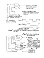
- FIG. 5 illustrates a preferred method for clocking the output control registers 37 and 38.
- a triple input NAND gate 74 in FIG. 5 has three input line signals: PUT STROBE/ signal; address signals for an external register (60 of FIG. 2); and the clock signal. These signals are correlated in FIG. 5.
- a Schott k y TTL NAND device 74 is used for the control register clock generator since the PUT Data" can be guaranteed for only 10 nanoseconds past the leading edge of CLOCK as received on the UIO-SM, and the output control registers require a data hold time of 2 nanoseconds minimum past the leading edge of their clock.
- the UIO-SM has the capability of directly addressing 0 to 64K words of program memory 50, FIG. 2, and from 0 to 32K words of data memory in RAM 90.
- the enabling of the program PROM 50 in the UIO-SM can be controlled by an expanded.memory in the application dependent logic 60 L .
- FIG. 6 illustrates how such an expanded memory can control the enabling of the UIO-SM program PROM 50 through the use of a front-plane external signal. If the expanded memory drives this signal to a "high" level, the UIO-SM program PROM 50 will be disabled. If the application dependent logic 60 L does not have a requirement for expanded memory, then it will simply tie this line to a logic "low”.
- a 5-input NOR gate 75 has inputs from program counter 41 in order to provide a parity disable signal (high) to disable PROM 50.
- the UIO-SM program PROM 50 may be expanded from 8K up to 64K words by using different size PROMs.
- the chip select and the addressing functions of the PROM 50 are automatically adjusted without circuit changes.
- a jumper arrangement is used to anable the parity bit output for the size of the program memory being used. With reference to FIG. 6, jumpers can be installed according to the following Table VI for each word size of PROM shown below.
- the UIO-SM receives its clock signal from the backplane of the UIO base module.
- the UIO-SM preferably uses Schottky type flip-flops followed by Schottky type inverters in order to generate the internal UIO-SM clock (CLOCK). All the timings are relative to this internal clock which preferably has a minimum delay of four nanoseconds and a maximum delay of 13 nanoseconds from the clock on the backplane.
- the application logic 60 L is preferably made to use the same type of devices to receive and distribute the clock.
- WAIT/ WAIT line
- This line is used such that when "slow memory” is addressed, the slow memory can force the UIO-SM to wait however long required for the "read” or the "write” to be valid.
- This line can also be used to halt the machine for any length of time required.
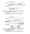
- the timing requirements for the WAIT/line are illustrated in FIG. 8. Since this line has multiple sources, including one line on the UIO-SM itself, it must be driven by an open-collector (TTL device).
- TTL device open-collector
- the state machine processor has a clock signal derived from the backplane of the base module. This clock, when not disabled, will execute data transfers from the I/O bus to external devices at the clock rate. But this rate would be too rapid for "slow" external devices to accept the high speed rate of the microprocessor.
- the application dependent logic module 60 L has Control Logic 66 (with an internal Address Decoder, FIG. 2) which recognizes any addresses directed to the external memory/external register means. These types of addresses originate from the memory reference register 40 or the instruction register 22. Upon recognition of addresses directed to external devices (external memory/external register means) the Control Logic 66 will initiate the WAIT signal to the microprocessor system which will "disable” the clock for one or more clock cycles. Thus, data to be transferred from the I/O bus will be held until the clock signal resumes. Depending on the "slowness" of the external devices, the WAIT signal can be programmed or set to disable 1, 2,...x clock cycles, thus to delay data transfer from the I/O bus 10 to the external devices.
- Control Logic 66 is connected to sense this, and can further maintain the WAIT signal longer until the external device is "ready” (not busy).
- a CLOCK enable (CLOCKENB) line is implemented on the UIO-SM for use in single pulse or for direct memory access (DMA) functions.
- the timing here is the same as the WAIT/ of FIG. 8.
- the timing relationships for the non-repeated GET's and PUT's are illustrated in FIG. 9.
- the WAIT line can be used on the GET to increase the memory write time in the case of a "slow" write memory.
- Another application for use of the WAIT line on GET's is to increase the amount of time available for the application dependent logic 60 L to drive the "GET DATA" and meet set-up times after having received the GET enable signal.
- the effect of the WAIT line is to increase the period of time that "PUT DATA" is on the I/O bus 10, although the UIO-SM would be halted during this time. It should also be noted that the timing of the PUT Strobe can only be guaranteed relative to the CLOCK signal and not relative to the PUT DATA. As such, neither edge of the PUT Strobe is used to directly clock the PUT Data into an application dependent register 60.
- the first transfer of data in a "repeated" GET to an addressed register in accumulator 30 will be invalid. All data transfers (after the first) will be valid.
- the same accumulator register 30 is addressed as a "destination" for each repeat GET operation.
- the memory reference register 40 will be incremented during each repeat GET operation, even though external RAM memory 90 is not used by the GET operator.
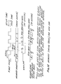
- the timing relationships for memory "Reads" in the UIO-SM are shown in FIG. 11.
- the WAIT line has been utilized on one of the memory reads to illustrate how one (or more) extra clock periods can be inserted after address stabilization to allow "slow access” memory to meet the setup time requirements of the UIO-SM.
- UIO-SM instructions which can do memory Write.s are: WRTW (Write Word), WR T B (Write Byte), and also GET.
- the WAIT line 11 has been utilized on one of the memory Writes to illustrate how one (or more) extra clock periods can be inserted after address stabilization in order to allow "slow" Write memory an adequate Write time.
- the repeated instruction itself can be halted by the application dependent logic 60 L .
- the application dependent logic produces the signal HLTREP/ (active low), which is the signal to the UIO-SM that halts the repetition. In FIG. 13 there is shown the timing of this signal. If the application dependent logic 60 L has no requirement for halting repeated instructions, then the application dependent logic can simply leave the HLTREP/ signal unconnected.
- the UIO-SM checks for odd parity and signals the results to the application dependent logic 60 L . If incorrect parity is detected, the UIO-SM takes no action other than to signal the error to the application dependent logic 60 L .
- This timing of the parity error line PARERR/ is shown in FIG. 14.
- MRR memory reference register 40
- M R R 15 the state of this line is loaded into M RR 40 at bit 15 whenever a loading of memory reference register 40 is called for by a UIO-SM instruction.
- the state of this line should be stable for at least 30 nanoseconds prior to the high transition of the clock to ensure that it can be operly loaded.
- This line is tied to ground (low side) if memory mapping is not used.
- IRQ/ On bus 11 which line is the "interrupt request line".
- This line is driven “low” preferably by an open-collector device in order to request an interrupt of the UIO-SM.
- the UIO-SM will only recognize an interrupt request if the interrupt mask is reset (EI instruction executed, Table XII-F, for resetting the interrupt mask bit) and an instruction fetch has just been completed when not in repeat mode (high clock transition at end of TO and the start of Tl).
- the U IO-SM responds to an interrupt by forcing execution of an ICALL instruction and switching the UIO-SM "background" mode "on".
- the ICALL instruction generates an acknowledge signal (ACKI/) in order to allow the application logic 60 L to place an interrupt call address on the I/O bus 10.
- the ICALL instruction saves the memory reference register 40 data in the MRR save register 47 and it saves the old P C (program counter) value on the stack before loading P C with the call address (placed on the I/ O bus 10 by the application logic 60 L ). Further interrupts are inhibited in the "background” mode and the duplicate set of flags (35) and accumulators (30 f ) are used so that the "foreground" operating environment is preserved therein.
- a return to the "foreground” mode is accomplished by executing an IRET instruction.
- the top value from the stack memory 45 is placed in the program counter PC 41 for the return address and the contents of the MRR save register 47 is placed into the memory reference register MRR 40.
- the original foreground flag 35 and foreground accumulator 30 f are again made active and contain the same values as before the interrupt.
- the clear line will place the UIO- SM in the "foreground” mode and set the interrupt mask to disable interrupts.
- the IRQ/line must be stable at least 60 nanoseconds before the leading edge (high transition) of the clock signal.
- the DMA request line 11 of FIG. 3 is a line which is driven “low” by the application dependent logic 60 L in order to isolate the UIO-SM address outputs on memory address bus line-16 so that direct memory access (DMA) logic can drive this bus. This line is left unconnected when not using the DMA.
- DMA direct memory access
- the bus enable line (BUSEN/LINE) from Control Logic 66 is driven “low” by the application logic 60 L in order to enable the I/O bus drivers on I/O bus 10, including data, GETENB, PUTSTB and REGADR signals.
- the GETENB is a signal used to indicate that GET data is driven on to the I/O bus 10;
- the PUTSTB is the signal used to indicate that PUT data is on the I/O bus 10;
- the REGADR signal is the signal used to indicate the enabling of the external register address lines for GET's and PUT's. When “high”, this line disables all I/O signals. This line is tied to "low” if it is not used.
- the front plane connectors (FIG. 4A, FIG. 4B-1, 4B-2) which provide the interface for the UIO-SM are preferably four in number wherein each of the four front plane connectors provides 25 pin connections on each of two sides of each front plane connector.
- Tables VII-X show the signal name for each pin number for each side of the four front plane connectors.
- the program counter 41 holds addresses which are used to select instruction data from the program memory 50. This program counter is reset to zero with the initiation of the "power on” signal and the clear signal.
- the command descriptor data will be transferred to an internal register of the microprocessor system, such as the accumulator register 30 where it can then be inspected and analyzed by the data manipulation circuitry (ALU 32) and the associated shift logic and byte swap circuitry 33, 34.
- ALU 32 data manipulation circuitry
- the meaning and intent of the descriptor command can be translated into instructions for the selection of a peripheral device, through its adapter, and for a subsequent transfer of data to or from the particular peripheral terminal device.
- the PUT operator is generated by the microprocessor and is applied to the application dependent logic module 60 L .
- An address (of a peripheral adapter and a peripheral terminal unit)will then be provided and the application dependent logic module will operate on this address to select the appropriate adapter and peripheral unit for data to be transferred.
- the software of the microprocesso system generates the PUT commands to the peripheral adapter.
- the microprocessor system When the microprocessor system generates a PUT operator to the application dependent logic module 60 L , then this enables the system to operate such that the host computer will send data on message level interface 105 to selected application dependent registers 60 where it can then be transferred into and stored in the external memory 90. As the microprocessor system provides a multiple series of repeated GET operators, then each word of data (or each byte of data if the peripheral can only accept bytes) will be transferred from the external register 60 to the selected peripheral terminal.
- the microprocessor operates much faster than the peripheral terminal, then what would generally be done is that if there is a multiple word transfer of data, is that the words would be stored in the external memory 90 and then fetched and transferred out to a selected peripheral at the slower speed with which the peripheral terminal device can accept the data.
- the external memory 90 acts as a storage buffer which permits the microprocessor to operate at its high speed while data can reside in the external memory 90 and then be transferred at a slower speed to the selected peripheral.
- Data will be sent from external memory 90 to the peripheral terminal by the use of a PUT operator which is used to control the peripheral adapter and terminal unit. That is to say, the PUT operator will command a word to be transferred from external memory 90 into a selected external register 60 and thence the peripheral.
- the PUT operator always deals with full "words" (AB).
- AB full "words”
- the microprocessor For byte-oriented usage, the microprocessor generates intervening instructions to isolate a "byte" from a memory word into a selected accumulator from which a PUT operation is then executed.
- the use of the memory reference register 40 is prominent here in that this register provides a source of addresses for the selection of operands and for the selection of programs which reside in the external memory 90.
- a series of GET operators will cause the transfer of the words stored in external memory 90 to the external register 60 and thence through the message level interface 105 over to the host system 100. Transfers to the host system will be done on a full word (two byte) basis, AB, in repetitive cycles since the host system can accept the complete 16 bit word AB.
- a multiple number of GET operators will cause the transfer of data from the peripheral terminal unit into the external memory 90 which acts as a buffer. Then a multiple number of PUT operators will be used to transfer this data from external memory 90 to the application register 60 and thence through the message level interface to the main host system 100.
- the adapters 109 c of FIG. 1 which are supplied for each of the peripheral devices are useful in accepting commands and for controlling operations of the particular peripheral. For example, at certain times it might be necessary to rewind the tape mechanism of a tape peripheral terminal unit or to eject or slew the paper on a printing device type terminal unit, or to select a certain address sector in the disk terminal unit.
- the UIO-SM has been implemented with several operators to simplify the processing of byte-oriented data even though the memory is organized in words which are two bytes wide. These particular operators work in conjunction with the memory reference register 40 of FIG. 2 which addresses external RAM data memory 90.
- the byte-oriented read/write operators use the "byte-swap" feature of the UIO-SM such that the "desired" byte is always read from external memory (90) into the "low order" byte of a selected register of the destination accumulator A(D) even though the desired byte might have been in the "high” order byte of the memory location in 90.
- the desired byte after being placed into the destination accumulator A(D), can then be processed.
- the high order byte of the accumulator A(D) must be updated with the other byte from the current data memory location, and then the two bytes are written into memory 90 as one word, and each byte will go into the proper position. This would be needed, for example, when a card reader peripheral is supplying only one byte of a word for each transfer operation.
- Table XIV shows a sequence of instructions and the resultant signals in the memory reference register 40, the accumulator register 30 and the data memory 90.
- the sequence shown in Table XIV starts with loading the memory reference register 40; reading the byte (RDB); translation; read before write byte (RDBW); write byte (WRTB); incrementing the memory reference register (MRR 40); again read byte (RDB); again translate; again read before write byte (RDBW); write byte (WRTB); incrementing memory reference register 40; read byte (RDB); translate;. read before write byte (RDBW); write byte (WRTB); and so on.
- Table XV shows the arrangement of data in a first Memory 1 and a second Memory 2 corresponding to true and false signals of the data memory address. Then the lower part of Table XV shows an exemplary sequence for the sequential instructions with reference to data in the memory reference register 40 and in the accumulator 30.
- F IG . 2C is a schematic block drawing of the Instruction Decoder 23 with its linear micro-sequencing circuit.
- a State Counter 23 s is initiated into a Fetch operation upon receipt of a Clear signal to its input.
- the State Counter 23 s feeds address bits to the PROM 23p which contains a set of internal micro-instructions.
- the PROM 23 P provides one output line designated Count Enable which is used to sequence the State Counter 23 .
- One set of instruction signal outputs selected from PROM 23p, are a set of control terms which are conveyed to a pipeline register 23 r which provides control signals to the units of the microprocessor and the application dependent logic 60 L .
- the pipeline register 23 r is used (a) to synchronize the output control term signals and also (b) to delay (by one clock) an output control term so that the signal from PROM 23p will be adequately stabilized.
- Another set of control signal terms are provided directly from the output lines of PROM 23 p .
- an alternate plug-compatible PROM 23 x can replace 23 P and be utilized by up to two extra address lines from State Counter 23 s . Each line (1 bit) will permit the addressing of an alternate or added set of instructions from PROm 23 x (in addition to using the original 2 bit lines).
- the Instruction Register 22 provides input instructions to PROM 23p.
- An input of 15 bits (instruction fields) is fed to Instruction Register 22 from either Program Memory 50 or external memory 90 depending on which memory has been selected as a source of data.
- One register of Instruction Register 22 is dedicated to receipt of the one bit of data called the "M" bit which is placed in each instruction word (from Program Memory 50).
- this field (M) is the one which selects either the Program Counter 41 or the Memory Reference Register 40 as the source of addresses to be next used for the selection of data.
- Condition Select Multiplexer 23 m has inputs from internal flag registers 35, 36, and from external flags 23 e in the Application Dependent Logic 60 L .
- the output of Condition Select Multiplexer 23 m is used to provide an input to PROM 23 of the linear micro-sequencer.
- FIG. 2C-1 is a schematic illustration indicating modes of the State Counter 23 s .
- state number 0 (upon activation of the Clear signal) a Fetch operation is initiated. Thence the "1" state is achieved where the instructions may start execution of an instruction.
- sequencer may . return to "0" for a Fetch and proceed to the "2" state.
- an operation step can occur.
- State Counter After completion of this cycle, the State Counter returns to "0" for another Fetch operation, or else sequence to state "3" which permits an additional set of operations as shown in FIG. 2C-1.
- FIG. 2C-1 showing the states "4", "5", “6” and “7” refer to the situation in FIG. 2C where an alternate larger instruction PROM 23x has been used to replace 23 p with the extra two address lines of 1 bit each for addressing the micro-instruction PROM.
- an alternate instruction set can be accessed and sequenced, similar to the sequencing of the PROM 23 p using the states 0 through 3.
- the State Counter 23 s can thus be used to address and select instructions from either PROM 23 p or from a larger PROM 23 x .
- the Instruction Register 22 is seen to provide a 5 bit address line to select an external register 60. There is further provided a 3 bit "source address” line and a 3 bit “destination address” line to Multiplexer 30 x (which is shown again in FIG. 2D).
- the accumulator registers 30 are seen clocked by a 8 megahertz clock, and also have a Write Enable (WE) input line coming from decoder-controller 23.
- WE Write Enable
- Multiplexer 30 x receives input addresses (from instruction register 22 ' ) for the source of data and for the destination of data.
- the SELECT line to MUX 30 x enables the source address to be read on the first half of the clock as seen in FIG. 2E at "Read”, and enables the destination address to be written on the second half of the clock at "Write”.
- the source location of data to be processed, and the destination location, where the data is to be placed are all accomplished in one clock (125 nanoseconds).
- a latch 30 is provided to the accumulator registers 30 to hold and convey data to ALU 32.
- the other data input to ALU 32 is from Memory Operand Register 31 which receives data and instructions along instruction bus 15 (from Program Memory 50), and/or memory data bus 12 (from external memory).
- the I/ O bus 10 provides a path for processed data to be fed back to accumulator registers 30 or to the external memory 90 or to the external registers 60 (of application dependent logic unit 60 L ).
- FIG. 2F there is seen a schematic drawing showing the intercooperation of the Repetition Counter 42 and Repeat Mode Flip-Flop 23 f and decoder-controller 23.
- FIG. 2F there will be seen another line for resetting (shutting off) the Repeat Mode Flip-Flop 23 f .
- Control Logic 66 This is done by using a HALT/REP signal from Control'Logic 66 in the Application Dependent Logic Unit 60 L . This could occur because Control Logic 66 has sensed an early ending in the data transfer operation.
- the linear micro-sequencer enables functions to be partitioned among the various PROMs so that each PROM will handle certain functions. There is no need for a stack memory or a next address register in the micro-sequencing circuitry.
- the micro-sequencer lowers the need for multiple IC's and permits expansion of PROM usage with no increase in hardware.
- microprocessor system permits simplicity and time-economy with which instructions can be fetched and executed, and data fetched and manipulated for data transfer purposes can be accomplished by what may be called (1) instruction pipelining and (2) operand pipelining.
- the processor while the processor is fetching an instruction in one clock, on the next clock, it is storing the result data in an I/O (peripheral) device by means of the I/O bus 10, or it may be storing the result data in the external memory 90, for example.
- another fetch cycle occurs which is a fetch cycle using a memory . address on the address bus 16 which will then-provide an output of memory data on the memory data bus 12.
- the external memory read path 12 is set separate from the memory write path 10 and the system can store the result data in a peripheral I/O device while at the same time reading instructions from memory.
- the instruction bus 15 feeds instructions to the instruction register 22.
- the memory operand register 31 also can receive operands from the memory data bus 12. Thus, on one clock the instruction bus can feed instructions to the instruction register (and then to instruction decoder-controller) while on the next clock the operand can be fed to the memory operand register 31 to facilitate the execution of the instructions.
- One level of the instruction pipelining includes (a) storing result data into the internal register files (as the accumulators 30 or the external registers 60) and (b) storage of results into an I/O port adapter which connects to peripheral devices.
- the operand pipeline uses the M bit.
- the M bit is used as part of the operand pipeline in order to determine which source of addressing will be used -- that is whether the memory reference register 40 will be used (data pointer) or whether the program counter 41 will be used (instruction pointer). Please refer to page 76 of specification on Byte oriented Read/Write operators. Note that the arithmetic logic unit 32 has the one input from the memory operand register 31 while the other input is from the accumulator registers 30.
Landscapes
- Engineering & Computer Science (AREA)
- Theoretical Computer Science (AREA)
- Physics & Mathematics (AREA)
- General Engineering & Computer Science (AREA)
- General Physics & Mathematics (AREA)
- Computer Hardware Design (AREA)
- Microelectronics & Electronic Packaging (AREA)
- Executing Machine-Instructions (AREA)
- Computer And Data Communications (AREA)
Abstract
Description
- This invention relates to peripheral controllers used in I/O systems for controlling data transfer operations between a main host computer and a plurality of peripheral terminal units.
- This application is a Continuation-In-Part of U.S. Serial No. 052,821, filed June 27, 1979, and entitled "Microprocessor System Operating With Normal or Slow Memories", inventors Brian K. Forbes and Robert D. Catiller.
- This application is related to the following patent applications filed as follows:
- A patent application entitled "Microprocessor System Facilitating Repetition of Instructions", inventors Robert D. Catiller and Brian K. Forbes, filed June 27, 1979, U.S. Serial No. 052,687.
- A patent application entitled "Microprocessor System with Source Address Selection", inventors Robert D. Catiller and Brian K. Forbes, filed June 27, 1979, U.S. Serial No. 052,477.
- A patent application entitled "Microprocessor Having Word and Byte Handling", inventors Robert D. Catiller and Brian K. Forbes, filed June 27, 1979, U.S. Serial No. 052,478.
- A patent application entitled "Digital System for Data Transfer Using Universal Input-Output Microprocessor", inventors Robert D. Catiller and Brian K. Forbes, filed June 27, 1979, U.S. Serial No. 052,336.
- A patent application entitled "Microprocessor System with Specialized Instruction Format", inventors Brian K. Forbes and Robert.D. Catiller, filed June 27, 1979, U.S. Serial No. 052,350.
- Certain pr.ior patents of the assignee of this invention form a background and understanding of the type of I/O systems used herein and these patents, listed below, are included herein by reference.
- U.S. Patent 4,162,520 to Darwen J. Cook and Donald Millers II entitled "Intelligent Input/Output Interface Control Unit for Input-Output Subsystem". This patent described a unit called a Data Link Processor for handling I/O data transfers.
- U.S. Patent'4,189,769 to Darwen J. Cook and Donald Millers II entitled "Input-Output Subsystem for Digital Data Processing System". This patent described peripheral-controllers organized into base module units to form an I/O subsystem.
- U.S. Patent 4,280,193 to Kenneth W. Baun and Jimmy G. Saunders entitled "Data Link Processor for Magnetic Tape Data Transfer System". This patent described a peripheral-controller made of a standardized card, called Common Front End, and a particularized card called the PDB or Peripheral-Dependent Board.
- Prior Art: Microprocessors and microprocessor systems will be seen to generally follow the architectural formulas and interrelationships which were established from general computer technology. However, microprocessors making use of large scale integrated techniques can be made into small packages with the use of integrated circuit chips and will generally follow the pattern of using a central processing unit, memory inptu-output circuits and various other control and support circuitry.
- It is typical that the architecture of microprocessors will generally use a program counter which is used to select some portion of memory to be addressed for retrieving program instruction codes to be executed.
- In the usage of a system where a central or main host processor operates in conjunction with a number of remotely located "base modules" which base modules support a group of peripheral-controllers which service and control external peripheral units, a considerable amount of circuitry has been required to provide data transfer capability on an efficient basis and also to cater to specific needs of each type of peripheral unit.
- Heretofore each peripheral-controller which was situated in a base module was burdened with many processor and control circuits for handling the specific requirements of each peripheral terminal unit_leading to a heavy burden of circuitry in each peripheral-controller.
- To alleviate the burden of costly circuitry for each peripheral controller, a universal or architecturally standard microprocessor was developed which would provide a multiplicity of processing functions for use in a peripheral-controller so that the peripheral-controller would only need a limited amount of application dependent logic and circuitry for handling the particular types of peripherals which it serviced. Thus, the universal processor or as it is called here, the "universal I/O state machine", could serve as a standard unit for all types of peripheral-controllers so that each of the peripheral- controlers would only need to have the minimum amount of circuitry and programs required for application to the particular peripherals in the network.
- Thus, with the use of the universal I/O state machine as a general purpose microprocessor in these applications, it became possible to reduce the cost, the quantity of circuitry, the space requirements and the system of architectural arrangements so that a more economical and more efficient architectural system could be established. Thus, with the advent of the described universal I/O state machine, there has been devised a generalized type of microprocessor which can serve as part of any type of peripheral-controller in a base module thus to handle any variety of peripheral terminal units. This generalized and simplified type of microprocessor (oriented to (a) addressing instructions and data and (b) manipulating data) executes its operations very rapidly and is designed to handle individual bytes for operations with peripheral devices which are "byte" oriented and also can execute processing and transfer operations with complete words (a word here being two 8-bit bytes symbolized as AB) for use with peripheral terminals which are "word oriented" and which can accept or transmit full words.
- The universal microprocessor working in conjunction with the peripheral-oriented application dependent logic module permits the development of a generalized type of peripheral-controller which can handle a plurality of peripheral units instead of requiring a separate controller for each peripheral unit. Since the hardware and programming of the microprocessor remains standard and constant for each of the peripheral-controllers while the application dependent module is programmed to cater to a group of selected peripherals, it is thus possible to accomplish not only great versatility in data transfer and control features but also to provide great economies in circuitry and cost.
- In digital systems where many instructions and control signals are required for the transfer of data to a variety of different types of peripheral units, generally a specifically tailored and designed peripheral-controller was provided.which is particularly suited to handle the data transfers to and from a single particular type of peripheral unit. It was found that by providing a uniform microprocessor for all types of peripheral-controllers which only varied in the type of application dependent logic programs required for specific types of peripheral devices, that great economies of space and cost could be realized. Thus, the combination of a universal microprocessor working in conjunction with an application dependent module could form a peripheral-controller to serve data transfer functions previously requiring a series of peripheral-controllers.
- The processor of the peripheral-controller of the present invention, upon receipt of an I/O data transfer command from a host computer, will generate instructions and execute data transfer operations to/from peripheral terminals by use of an application dependent logic module which provides an external memory with instructions for peripheral terminal control and which has control logic which recognizes when slow devices are addressed. The control logic can then initiate a WAIT signal to said universal processor slow down and regulate the rate of data transfers to slow memory and slow peripheral terminals.
- A linear microsequencer circuit operates a decoder-controller in the microprocessor. The microsequencer includes a micro-instruction PROM which is sequentially stepped by a State Counter after being initiated by the "Clear" signal. The micro-instruction PROM also receives signals from an instruction register and flag registers. The micro-instruction PROM then provides Control Term signals for operation of the microprocessor system.
-
- FIG. 1 is an overall block diagram illustrating the use of a main host system computer with a plurality of base modules which support peripheral-controllers which communicate with peripheral devices.
- FIG. 2 is a diagram of the peripheral-controller showing the elements of the universal input-output microprocessor state machine and its communication lines to the application dependent logic module. FIG. 2 is subdivided into two portions designated as FIG. 2A and FIG. 2B such that by juxtaposing FIG. 2A to the left of FIG. 2B (and
- FIG. 2B to the right of FIG. 2A) the continuity of connections between the two drawings may be seen. FIG. 2C is a schematic drawing of the decoder-controller with its linear sequencer circuitry; FIG. 2C-1 shows the state counts; FIG. 2D illustrates the addressing of selected accumulator registers and their relation to the arithmetic logic unit and I/O bus; FIG. 2E shows how source and destination addresses are accessed in one clock period;
- FIG. 2F is a schematic drawing illustrating the relationship between the repetition counter and repeat-mode flip-flop.
- FIG. 3 is a schematic diagram showing certain memory addressing features of the UIO-State Machine, particularly the use of a dedicated bit designated as the "byte-swap" bit.
- FIG. 4A is a perspective drawing of the input- output base module and showing major elements such as the distribution control card, the peripheral controller (line control processor) card and certain connections from the front plane (fore plane) to the host computer and to peripheral units. FIG. 4B is a schematic drawing showing circuit connections to the four front plane connectors. FIG. 4B is oriented such that it shows the first front plane connector while FIG. 4B-1 shows the second front plane connector. Orientation-wise the FIG. 4B-1 can be 5 juxtaposed underneath the FIG. 4B in order to provide continuity to the connections shown between the two front plane connectors. FIG. 4B-2 illustrates connections to the front plane connector No. 3 and FIG. 4B-3 illustrates the connections to the front plane connector No. 4.
- FIG. 5 is a timing diagram showing the clocking of output control registers of the UIO-state machine.
- FIG. 6 -is a circuit drawing showing how the program memory is enabled.
- FIG. 7 is a timing diagram for the clear line.
- 5 FIG. 8 is a timing diagram showing the WAIT line timing.
- FIG. 9 is a timing diagram showing timing for non-repeated GET/PUT functions.
- FIG. 10 shows the timing diagrams for the repeated 0 GET/PUT functions.
- FIG. 11 is a diagram showing the correlated timing features for reading data from external memory on the memory data bus.
- FIG. 12 is a timing diagram showing the timing correlations between the clock, the memory address signal and the memory write data on the I/O bus.
- FIG. 13 is a timing diagram showing the relationship of the halt repetition function signal to the clock.
- FIG. 14 is a timing diagram showing the relationship of the parity error signal to the clock and memory address signal.
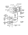
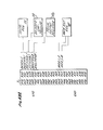
- Referring to FIG. 1, there is seen a system block diagram of a typical Burroughs host computer system, with central
processing unit cabinet 100 having basically a series of main memory modules 101, amemory control module 102, adata processor module 103, working in cooperation with a hostdependent port module 104. The host dependent port module provides a series ofcommunication cables 105 designated as MLI or message level interfaces. These message level interfaces provide communication lines to a base module cabinet 106 (or a plurality of such cabinets) which are designated as the Universal Input/Output Base Module Cabinet. The base module cabinet is built to support a plurality of universal input/output (UIO)base modules 107. Each of these UIO base modules provides communication, control, and data transfer lines to specific types of peripheral devices. - It should be noted that the host dependent port module can have message level interfaces to a plurality of UIO base module cabinets. And likewise, each UIO base module cabinet may have message level interface communication lines to other host systems 200 (main memory and processor) in addition to the first described host system of FIG. 1.
- In the preferred embodiment of the system to be described herein, it will be seen that a base module cabinet can support from one to four UIO base modules. Formerly each of the UIO base modules contained up to eight peripheral-
controllers 108 known as "line control processors" and each of the line control processors were dedicated to data transfer and control with a particular type ofperipheral device 109. This plurality of separate peripheral-controllers for each different peripheral has now been replaced with a single universal microprocessor and application dependent logic module which constitutes a single peripheral-controller for handling a plurality of peripheral terminals. - Another provision of the system will allow for a unit designated as a line expansion module (LEM) which can be inserted in the UIO base module so that a single message level interface can be extended to communicate with up to eight UIO base modules.
- The host system as represented by the central
processing unit cabinet 100 can communicate with up to 64 peripheral controllers (line control processors) for each message level interface (MLI), if the base module is provided with the unit known as an LEM or line expansion module. - As seen in FIG. 1, the
host system 100 can have eight message level interfaces (HLI) and can thus communicate with up to 512 peripheral controllers (line control processors). - The peripheral controllers or line control processors 5 (LCP) are controllers which are dedicated to data transfer and control between a peripheral terminal and the main host system or a plurality of host systems.
- The peripheral controllers known as line control processors have been described, both in their system interrelationships and in their internal workings, in a number of previously filed patent applications and issued patents. These include the following United States Patents: U.S. Patent 4,174,352 entitled "Modular Block Unit for I/O Subsystem", inventors Darwen J. Cook and Donald A. Millers, II; U.S. Patent 4,106,092 entitled "Interface System Providing Interfaces to Central Processing Units and Modular Processor-Controllers for an Input-Output Subsystem", inventor Donald A. Millers, II; U.S. Patent 4,162,520 entitled "Intelligent Input-Output Interface Control Unit for Input- Output Subsystem", inventors Darwen J. Cook and Donald A. Millers, II; and U.S. Patent 4,189,769, entitled "I/O Subsystem for Digital Data Processing System", inventors Darwen J. Cook and Donald A. Millers, II, and these patents are included herein by reference.
- The peripheral controllers known as line control processors (LCP's) may generally fall into types of categories. There is the 2-card LCP and the 3-card LCP.
- This peripheral controller has a first card which is designated as the CFE or common front-end on which there are supplied a plurality of read-only memories (ROM's); hardware-wise these common front-end cards are of the same construction and nature except that in individual cases the ROMs are made to hold different programs which are suitable to the application at hand or the peripheral device with which it is used; thus, hardware-wise all the front-end cards will be found to be the same physically but only differ in the fact that different program material is inserted in the individual ROMs. The second card in the 2-card LCP is the PDC or peripheral dependent card. This card is uniquely built and adapted to suit the particular type of peripheral unit to which it communicates. It may be designated as an "application dependent logic module" .
- Here, again, the first card is the CFE or common - 5 front-end card which is physically the same except for different programming, inside the ROM, this program being varied according to the application required. The second card is the CDC or common data card which is tailored to suit the requirements of different peripheral units; however, it 0 may be the same for such a group of items as magnetic tape, punched card-tape, disk pack, and console controls. The third card of the 3-card LCP is designated as the PDC or peripheral dependent card. This card is unique and is designed to handle one particular type of peripheral device.
- In FIG. 4A there is seen a more detailed perspective drawing of a typical I/
O base module 107. A plurality of these base modules are housed and serviced by a base module cabinet 126 of FIG. 1. - The
base module 107 provides housing whereby printed circuit cards holding integrated circuitry may be inserted on sliding tracks in order to connect with the backplane connectors for automatic connection into the system. A peripheral controller (or line control processor) 108 may require, as previously described, two printed circuit or three printed circuit cards. The base module may support up to eight such peripheral controllers in its housing. Communications between.the base module and the host system are controlled bydistribution card 110. Other specialized handling printed circuit cards may be inserted, such as the previously mentioned line expansion module, common front-end card, common data card; or a second distribution control card, etc., can be inserted for connection into saidbase module 107. - The frontplane or foreplane permits jumper cable connections 111 (FIG. 4A) between printed circuit cards and also permits connection cables such as
message level interface 105 to the host computer orribbon cable 109c to permit connection from the base module to external devices such asperipheral device 109. - An
interface panel 106 may be provided on the base module cabinet 120 to provide for cable connectors such as 104cc' 109 to facilitate disassembly and reconnection. cc - As was described in the previously mentioned patent references regarding line control processors, each base module unit is provided with a
Distribution Control Card 110, FIG. 4A, which connects the message level interface from the main host system to a selectively addressed line control processor (peripheral controller) in that base module. Further, the base module has a common maintenance card and a common termination card which acts in common to service the entire group of up to eight line control processors in a base module. - The UIO base module may also support a line expansion module or LEM. This feature expands the usage of a UIO base module by adding another Distribution Control Card which permits connection of that base module to yet another main host system in addition to the one already connected to the first Distribution Control Card. Thus, communication from a main host system can be expanded to cover two or more UIO base modules and their attendant line control processors. Likewise, two or more host systems can be made to communicate to a UIO base module or a plurality of such base modules.
- When it is desired to have one UIO base module connected to two main host computers, then a control card is used which is called the BCC or base control card. The base control card serves two basic functions; (a) to provide an interlock when multiple host computers try to access a base module, so that line control processors can thus be locked out from use by unauthorized host computers, and (b) to provide assorted features such as a base identification (ID) number and for maintenance control. The BCC is not mandatory when multiple hosts are connected to a base; however, it is useful. The base control card, however, can also be used when only a single host computer is connected to the UIO base module. Thus, the BCC is an independent and optional module, as is the line expansion module LEM.
- Thus, in reference to FIG. 1, it should be stated that when a host computer is connected to a UIO base module, the base module must.have at least one
distribution card 110, FIG. 4A, for each host computer which is connected to it. Now, when a UIO base module is connected to a multiple number of host computers, then there is need for the base module to be provided with a unit known as the PSM or path selection module. The path selection module is the control unit which regulates the communication to and from the multiple number of distribution cards in the UIO base module. - In the development of line control processors, such as indicated in the prior cited patents and references, it was found that the amount of logic required for adaptability to any given type of peripheral unit or to a variety of peripheral units required that expensive and space consuming logic circuitry be developed which would take large quantities' of hardware and space requirements on printed circuit cards such that sometimes four or five extra logic cards were needed in order to complete a particular line control processor. Soon the cost and space requirements of these developments became prohibitive and better means were required for handling the variety of functions required of a line control processor.
- In this situation a microprocessor-controller was developed which could handle all the basic logic for any variety of peripheral terminal units and which could be built with a minimum amount of components and placed on a single printed circuit card. This device was designated as the universal input/output state machine or UIO-SM. Thus, the UIO state machine could be built typically on a 112 chip circuit board and be placed within the slide-in card rack which is supported by the LCP base module (now called UIO base module). The UIO state machine can interface easily to any application dependent logic through its front plane and, except for power connections and clock connections, no connections needed to be made to the LCP or UIO base backplane. The universal I/O state machine is basically implemented in transistor type logic (TTL).
- The UIO-SM has been made to implement a useful group of general purpose operators which include:
- Arithmetic OP's
- Logical OP's
- Read/Write Memory OP's
- PUT/GET OP's
- Program Stack OP's (Branch, Call and Return)
- In FIG. 2, there is shown a schematic diagram,of a peripheral-controller for the I/O Subsystem of the present invention. The peripheral-controller is composed of a U
IO State Machine 1 and an associated ApplicationDependent Logic Module 60L which provides anexternal memory 90,control logic 66 andexternal registers 60 which connect to hostsystem 10 and to peripheral 109 (via adapter 109c)· - Referring to FIG. 2, the
UIO State Machine 1 is seen to be provided with Instruction-Execution Logic 2,Memory Address Logic 3,Data Manipulation Logic 4, and aninternal program memory 50. - In FIG. 2 the Application
Dependent Logic Module 60L is connected bybusses State Machine 1. TheLogic Module 60L provides anexternal memory 90 plus bus logic 66' andinterface control logic 66 which includes anaddress decoder 66ad for sensing addresses of "slow" elements, and anexternal register 60 which has bus connections to theHost System 10 and Peripheral Terminals such as 109. - At FIGS. 2A and 2B there is seen an overall block diagram of the UIO state machine. The input/output lines at the bottom of the drawing are all front plane lines which connect to the peripheral's application dependent control (PDC) logic since it is desired that the UIO state machine itself be independent of any application type logic or of the special requirements of particular peripheral units.
- Referring to the state machine block diagram of FIGS. 2A and 2B there will be seen a series of interconnecting
lines 16, 171, 172' 18, 10, 19, 11, 12 and 20, which connect to the applicationdependent logic 60L .These lines are labeled, such as the external memorydata output bus 12, the I/O and memory writeparity line 18, thememory address bus 16, the memory write enable 19 (and other functions listed on FIG. 2), the direct memory access (DMA) request line 11 (and other functions on FIG. 2), in addition to the main I/O bus 10.Line 15 is the instruction output bus from theprogram PROM 50. - A
program counter 41, having input lines fromstack memory 45 and I/O bus 10, via 10f' provides an output line which feeds an input signal to the program PROM 50 (internal memory 50). A memory reference register 40 (MRR) receives its input signals via I/O bus 10 from accumulator registers 30,memory operand 31, and the save-MRR 47 (memory reference register-save). Repetition counter 42 also receives an input line via I/O bus 10 for signals from accumulator registers 30 andmemory operand 31. - The
stack memory 45, controlled bystack pointer 46, provides an output line to theprogram counter 41. Therepetition counter 42 provides an output which feeds back aroundline 10f over to the I/O bus 10 and also around to the accumulator registers 30. - Attached and receiving input from the I/
O bus 10 is acontrol register 1 designated asitem 37, acontrol register 2 designated asitem 38 and aparity register 39. The control registers 37, 38 provide buffering of signals to application control register lines 171, 172. Theparity generator 39 has 5 an output line 18 (part of I/O bus 10) and provides "I/O and memory write" parity. - The memory
output data bus 12 from RAMexternal memory 90 connects to thememory operand register 31 whose outputs feed toALU 32 andparity check circuitry 21 which 0 has anoutput line 20 to provide memory read parity toexternal memory 90.Data bus 12 also provides an input to theinstruction register 22 which has an output line connecting to the input of the instruction decoder-controller 23. Situated within instruction decoder-controller 23 are 5 external flag registers 23e' interruptmask 23i' andstate counter 23s. - Accumulator registers 30 actually comprise two sets of eight registers, one set designated 30f (foreground accumulator registers) and the other set as 30b (background). Each of the 16 registers are addressed and selected by an
address line 23a from the instruction decoder-controller 23. - The I/
O bus 10 provides a channel to the accumulator registers 30 which have an output to the B input of thearithmetic logic unit 32. Another input A to thearithmetic logic unit 32 comes from thememory operand register 31 which gets its input from external memory via thememory output bus 12, or from internal memory viabus 15. - The arithmetic logic unit 32 (ALU) has one set of outputs which feed to the "foreground"
flag register 35 and another set of outputs to the "background"flag register 36. These flag registers 35 and 36 form an output which is fed to the instruction decoder-controller 23. They are used to signal "foreground mode" conditions for normal operation and "background mode" conditions for interrupts or emergency operation. - The F output of the.
arithmetic logic unit 32 feeds on abus 10. to theshift logic circuitry 33 and to the byte-swap circuitry 34. The outputs of thesecircuits O bus 10. - The PUT OP (operator) writes a 16-bit word (two bytes symbolized as AB) from the I/
O bus 10 into a selected application dependent register 60 (external register), the particular register being addressed via GET-PUT address lines 19. The PUT OP can address any one of 32 application dependent registers. The GET OP reads a 16-bit word from a selected applicationdependent register 60 into anaccumulator register 30 on the UIO-SM or intoRAM memory 90 through the I/O bus 10. The GET OP can also address a selected one of the 32 application dependent registers 60 (external registers). - The UIO-SM has the ability to repeat certain OP's (PUT's, GET's and logical OP's) by loading a number N (from the software) into a
repetition counter 42 to control the memory reference register (MRR) 40 which is used as a counter after having been loaded with the starting address of the data block to be used in the "repeated" OP. A more detailed discussion of this operation is presented hereinafter in connection with FIG. 2F. - In order to hold "PUT Data" for a longer period of time than can occur directly off of I/
O bus 10, there are two 8-bit registers (control registers 37, 38) which have been placed in the UIO-SM. The strobing of theseregisters - A "WAIT line" (on bus 11) has been built into the UIO-SM such that when an external "slow memory" is addressed, ; the "slow memory" can force the UIO-SM to wait however long required for the Read or the Write to be valid. This is seen on FIG. 2 at
bus 11 which feeds signals to the instruction decoder-controller 23. This line can also be used to halt the machine. A clock enable line on bus 11 (CLKENB) has been included so that the applicationdependent logic 60L may control the state machine clock for single pulse operations and also direct memory access (DMA) operations. The timing for this signal is the same as the WAIT signal onbus 11. - As seen in the state machine diagram of FIG. 2, the UIO-SM can check via
circuitry 21 for odd parity on each memory fetch. All memory fetches fromexternal memory 90 come on the memory output data bus which is shown asbus 12 and which connects toinstruction register 22 and to thememory operand register 31. All memory writes go out on the I/O bus 10 along with odd parity online 18. The UIO-SM contains 8-K words of user-defined instruction programs inPROM 50 which is capable of being expanded to 64-K words. - With reference to FIG. 3, it will be seen that memory addresses can come from two sources -- the
program counter 41 and the memory reference register (MRR) 40. The UIO-SM provides the ability to do condition and unconditional Branches, Calls and Returns. "Calls" can be nested up to 16 levels fromstack memory 45. Thememory reference register 40 stores addresses and is used (at certain times specified in instruction words) to addressRAM data memory 90 which will provide programs applicable to the peripheral device connecting to the applicationdependent logic module 60L. Thisexternal memory 90 also serves to store data which is being transferred between the host computer and the peripheral terminal device. Sincememory memory 90. The low order bit (BYTESWP) is used by the byte-oriented read/write OP's to determine whether or not to byte-swap the two byte data word before storage into accumulator registers 30 on an "external data memory read" or before storage into externalRAM data memory 90 on a "data memory write". This particular feature permits the UIO-SM to easily handle byte-oriented data in that the desired byte is automatically read into the "low order" byte position of the accumulator registers 30 on "data memory reads", as well as being automatically written from the "low order" byte position into the correct byte position on "data memory writes". The "high order" byte position of the accumulator registers 30 must contain the last byte written, if any is present. - In Table I there is shown the instruction format for the UIO-state machine operators. The external memory
output data bus 12, or internalmemory instruction bus 15, provides 17 bits designated 0-16. The bus bits 0-7 (low order) constitute the "B" byte while the bus bits 8-15 constitute the "A" byte (high order).
- As will be seen from Table I certain fields are specified such as the P field for odd parity, the basic function field Fl, F0, and function variant field by V4-VO. The destination specifier field is designated D3-D0; the source accumulator field is designated S2, Sl, S0. The field which causes selection of the memory address source to be used in fetching the operand of the instruction is designated M; while the function field for copying the arithmetic logic unit output into the
memory reference register 40 is designated by the field C. - The odd parity bit is set such that an odd number of 1's will exist across the entire 17-bit instruction (or the operand). The basic function field Fl, FO is described in Table II such that various binary digit combinations of Fl, FO provide certain functions as shown.

- For example, the GET function provides for the transfer of the contents of an
external register 60 to theaccumulator 30 or to RAMmemory 90. Thedigital bits 0, 1 provide for the transfer of the contents of an addressed register in accumulator 30 (or an addressed portion of external RAM memory 90) to the external registers 60. This is called the PUT function. TheF field bits 1, 0 provide for execution of the arithmetic logic unit operators ; whilebits - Table III shows the function variant field V4-VO and its relation to the function field F1, F0.
-

bits 0, 1 specify a PUT operation into an external register of a specified address. - Table IV shows the destination specifier field, D3, D2, D1, D0.

- This D3-DO field is subdivided into (i) GET and ALU OP's and (ii) PUT and program stack OP's. In the case of (i) there may be no destination specified; or only a miscellaneous control field may be used to update the flag register ; or the destination may be the
RAM memory 90. - In the case (ii) for the destination field, the operand source may come from
RAM memory 90; or the operand source may be from thesource accumulator 30; or the destination may be a load into therepetition counter 42. - The Source Accumulator Field S2, S1, SO is shown in Table V below:

- The source accumulator field specified as S2, S1, SO (Table V) may apply (i) to the ALU or the PUT Op where the operand from the source accumulator A(S) can be the same as the destination accumulator A(D); or (ii) where the GET Op can function so that the source is an
external application register 60 or that the source is therepetition counter 42; or wherein (iii) the program stack Op's can provide a return operator or an ICall operator. - The M field specifier (as originally noted in Table I) may occur as one of two binary states, that is as a 0 or as a 1. When M is 0, then the operand for this instruction is located one address beyond this instruction (PC + 1, program counter plus 1) or there is no operand. If the instruction does not require a memory operand, then PC + 1 is not used for an operand; the next "instruction" will be at PC + 1 (no space is allowed for an operand). The operators that do not use an operand are listed as follows:
- 1. All "GET" operators;
- 2. "PUT" operators with D3 = 1;
- 3. "CALL" or "BRANCH" with D3 = 1;
- 4. ICALL, RETURN, RETURN, ROTR, SHFL, SHFR, CMA, ONES, ZERO, SWAC, WRTW , WRTB , DRTL, EI, DI and RSTK Operators. (These operators are discussed subsequently hereinafter).
- When the M field bit is "1", then the operand for this instruction is addressed by the memory reference register 40 (MRR) or else there is no memory operand for this instruction.
- The C field originally shown in Table I may read as a 1 bit or a 0 bit. In the 1 bit situation this means that the machine will not copy the ALU output to the
memory reference register 40; however, if the bit is "0", then the ALU output will be copied on to thememory reference register 40. The C bit can be set to 0 on all instructions except GET's and RDB, RDBW', RBWR, SWAC and WRTB. These operators are discussed subsequently hereinafter. - Two flag registers are provided so that at least one flag register is fully available for each of the two operating modes. Thus,
flag register 35 is the "foreground mode" flag used under normal operating conditions whileregister 36 is the "background mode" flag which is used during interrupt or other unusual conditions. As seen in FIG. 2, flag registers 35, 36 receive output from thearithmetic logic unit 32 and provide an output line to feed input to the instruction decoder-controller 23. The flag register is updated at the end if all ALU operators (which include arithmetic OP's, logical OP's and loa /store/move OP's). On OP's which "byte swap" theALU 32 output before storage into the destination location, the flag register is updated on the basis of the full two bytes of information from theALU 32 after being swa ped. In the specific cases of REBW OP (read before write byte) and the RBWR OP (read before write byte reversed) , a full memory word is read into the UIO state machine, but only one of the two bytes read is written into accumulator register 30 (the low order byte of the accumulator destination register remains unchanged). The flag registers (35,36) are updated on the basis of the full word read fromRAM memory 90. - As indicated in FIG. 2, the accumulator registers 30 actually constitute two different sets of eight registers. One set 30 f of accumulator registers is for normal operating conditions (foreground mode) while the
other set 30b of eight accumulator registers is for abnormal conditions (background mode) as during interrupts. - The use of the
repetition counter 42 provides an instruction repetition feature where a PUT or a GET OP may be repeated up to 256 times by the use of a PUT OP to load the repetition counter 42 which must be followed by the PUT or the GET OP to be repeated. Any value N from 0 to 255 (from the software) may be loaded into therepetition counter 42 and N + 1 operations will be performed (1 to 256). The address source for the repeated PUT data or the address destination for the repeated GET data is found inMRR 40 and thus these addresses will originate from thememory reference register 40 and not from the program counter 41 (PC + 1) . In other words, the M-bit is set to "1" in the repeated PUT or GET. After each PUT or GET OPs, the hardware will increment theMRR 40 in preparation for the next PUT or GET. When repeated, each individual PUT or GET will execute in one clock period, unless the PUT or the GET addresses a "slow memory", in which case there will be one extra clock period at the beginning of the repeated PUT's or at the end of the repeated GET's. - The use of the repeated PUT's or GET's serves to greatly increase code compaction while also greatly increasing the speed of the clock transfers to or from
RAM memory 90. - Any logical OP (AND, CMA, CMM, OR,XOR, ONES, ZERO, ADDC, SUBC, etc. as described hereinafter) may be repeated up to 256 times by the use of a PUT OP to load the repetition counter 42 which must be followed by the logical OP to be repeated. Any value of N from 0 to 255 may be loaded into the
repetition counter 42 and N + 1 operations will be performed (1 to 256). For the repeated OP to work as expected, thesource accumulator 30 should be equal to thedestination accumulator 30. The address source for the operand data should originate from the memory reference register 40 (MRR) just as for the repeated PUT or GET. After each OP of the repeat sequence is executed, the hardware willincrement MRR 40 in preparation for the next OP. When repeated, each individual logical OP will execute in one clock period, unless the operands are located in a "slow memory". - One particular case, where a repeated logical OP can increase code compaction and execution speed, is the use of the repeated "Exclusive OR" for the purpose of generating longitudinal parity on a data block located in
external memory 90. - The PUT OP which loads the
repetition counter 42 must have the N value in the "B" byte (low order 8-bits) of the PUT data. The "A" byte (high order 8-bits) is a "don't care". - The application
dependent logic 60L has the capability of stopping instruction repetition. even though the full number of operations has not occurred as will be later discussed in connection with FIG. 2F. - The capability exists to do repeat operations with PC (program counter 41) used for the memory operand source address (M-bit equal to 0). In this case,
PC 41 will increment during the repeat operation instead of MRR 40 (provided that the operator does use a memory operand). UsingPC 41 during the repeated operations will allow the use of a multiple word literal following the single repeated operator. The size of the "literal" field must be exactly the number of words specified by the repeat count value plus 1 word. The HLT REP / interface line (halt repetition) must remain "high" during all repeatoperations using PC 41 as an address source for operand data. - In regard to the instruction execution speed, the basic clock rate for the UIO-SM is 8 MHZ (125 nanosecond clock period). All OP's, with the exception of the program stack operators, execute in two clock periods except such OP's that write from the UIO-
SM accumulators 30 into RAM memory 90 (3 clocks required) or have operands to be fetched from or stored into "slow memory" (three or more clocks required). The program stack operators require 3 clock periods to execute if the condition is true (Branch or Call "executed") and only require 2 clock periods if the condition is false (Branch or Call "not executed"). The NO-OP executes in 2 clock periods. The OP IReturn executes in 3 clock periods, while Load and Store Accumulator executes in 4 clock periods. - The execution of any given instruction requires an "instruction fetch" along with the above-noted execution cycles; however, in the case of the UIO-SM, the instruction fetch for the next instruction is performed during the last execute cycle of the current instruction. Therefore, the "instruction fetch" is masked from the timing.
- The NO-OP consists of any program stack operator (such as Branch) with the condition test field set to "UNCONDITIONAL" and the destination specifier set to "EXECUTE ON CONDITION TEST NOT TRUE" (Branch never). Whether or not the NO-OP occupies one or occupies two memory locations, is a function of whether or not the operand (Branch never address) is located next to the instruction (PC + 1) or is addressed by the
memory reference register 40 or comes from anaccumulator 30. The flag registers 35, 36 will not be updated on the NO-OP. - The clear sequence is a "zeroing" operation. When a "Clear" is issued to the UIO-SM, the
program counter 41, therepetition counter 42, and thestack pointer 46 are reset to zero and an instruction is fetched. After a "Power-up Clear" has been issued, theaccumulators 30 cannot be predicted. However, if a "Clear" is issued while power remains up, the accumulator registers 30 will retain their states just previous to the "Clear". While "Clear" is true, at least two clocks must be issued; after "Clear" has gone false, one clock is required before execution of the first instruction begins. - There are two output control registers 37 and 38 in the UIO-SM as seen in FIG. 2. These can be used by the application
dependent logic 60L to hold "PUT Data" for a longer period of time than can normally occur directly off of the I/O bus 10. Both output control registers 37 and 38 are 8-bits wide and have their data inputs connected to thelow order 8 bits of the I/O bus 10 ("B" byte). Both of these output control registers must be clocked by the applicationdependent logic 60L. FIG. 5 illustrates a preferred method for clocking the output control registers 37 and 38. A tripleinput NAND gate 74 in FIG. 5 has three input line signals: PUT STROBE/ signal; address signals for an external register (60 of FIG. 2); and the clock signal. These signals are correlated in FIG. 5. - Once clocked by a leading edge, the outputs of these registers will stabilize in 17 nanoseconds or less A Schottky
TTL NAND device 74 is used for the control register clock generator since the PUT Data" can be guaranteed for only 10 nanoseconds past the leading edge of CLOCK as received on the UIO-SM, and the output control registers require a data hold time of 2 nanoseconds minimum past the leading edge of their clock. - In the preferred embodiment and without expansion of memory, the UIO-SM has the capability of directly addressing 0 to 64K words of
program memory 50, FIG. 2, and from 0 to 32K words of data memory inRAM 90. To facilitate any further expansion of memory, such as by using paging techniques or otherwise, the enabling of theprogram PROM 50 in the UIO-SM can be controlled by an expanded.memory in the application dependent logic 60 L. - FIG. 6 illustrates how such an expanded memory can control the enabling of the UIO-
SM program PROM 50 through the use of a front-plane external signal. If the expanded memory drives this signal to a "high" level, the UIO-SM program PROM 50 will be disabled. If the applicationdependent logic 60L does not have a requirement for expanded memory, then it will simply tie this line to a logic "low". In FIG. 6, a 5-input NORgate 75 has inputs fromprogram counter 41 in order to provide a parity disable signal (high) to disablePROM 50. - The UIO-
SM program PROM 50 may be expanded from 8K up to 64K words by using different size PROMs. The chip select and the addressing functions of thePROM 50 are automatically adjusted without circuit changes. A jumper arrangement is used to anable the parity bit output for the size of the program memory being used. With reference to FIG. 6, jumpers can be installed according to the following Table VI for each word size of PROM shown below.
- The UIO-SM receives its clock signal from the backplane of the UIO base module. To receive clock signals, the UIO-SM preferably uses Schottky type flip-flops followed by Schottky type inverters in order to generate the internal UIO-SM clock (CLOCK). All the timings are relative to this internal clock which preferably has a minimum delay of four nanoseconds and a maximum delay of 13 nanoseconds from the clock on the backplane. In order to insure minimum clock skew between the
application logic 60L and the UIO-SM, theapplication logic 60L is preferably made to use the same type of devices to receive and distribute the clock. - The following paragraphs will illustrate detailed timing and explanation for the interface between the UIO-SM and the application
dependent logic 60L. - Referring to FIG. 7, which is entitled "Clear Line Timing", it will be seen that in order to initialize the UIO-SM, the CLEAR line must be "true" (active low) .for at least two full clock periods.
- Another feature implemented into the UIO-SM is the WAIT line (WAIT/). This is used such that when "slow memory" is addressed, the slow memory can force the UIO-SM to wait however long required for the "read" or the "write" to be valid. This line can also be used to halt the machine for any length of time required. The timing requirements for the WAIT/line are illustrated in FIG. 8. Since this line has multiple sources, including one line on the UIO-SM itself, it must be driven by an open-collector (TTL device).
- Referring to FIG. 3, the state machine processor has a clock signal derived from the backplane of the base module. This clock, when not disabled, will execute data transfers from the I/O bus to external devices at the clock rate. But this rate would be too rapid for "slow" external devices to accept the high speed rate of the microprocessor.
- The application dependent logic module 60L (FIGS. 2A-2B) has Control Logic 66 (with an internal Address Decoder, FIG. 2) which recognizes any addresses directed to the external memory/external register means. These types of addresses originate from the
memory reference register 40 or theinstruction register 22. Upon recognition of addresses directed to external devices (external memory/external register means) theControl Logic 66 will initiate the WAIT signal to the microprocessor system which will "disable" the clock for one or more clock cycles. Thus, data to be transferred from the I/O bus will be held until the clock signal resumes. Depending on the "slowness" of the external devices, the WAIT signal can be programmed or set to disable 1, 2,...x clock cycles, thus to delay data transfer from the I/O bus 10 to the external devices. - In addition, if the external devices are busy (not ready) the
Control Logic 66 is connected to sense this, and can further maintain the WAIT signal longer until the external device is "ready" (not busy). - When the WAIT signal is shut off by the
Control Logic 66, then the clock signal in the microprocessor system resumes, and data transfers again are effectuated. - A CLOCK enable (CLOCKENB) line is implemented on the UIO-SM for use in single pulse or for direct memory access (DMA) functions. The timing here is the same as the WAIT/ of FIG. 8.
- The timing relationships for the non-repeated GET's and PUT's are illustrated in FIG. 9. The WAIT line can be used on the GET to increase the memory write time in the case of a "slow" write memory. Another application for use of the WAIT line on GET's is to increase the amount of time available for the application
dependent logic 60L to drive the "GET DATA" and meet set-up times after having received the GET enable signal. - In the case of the PUT OP, the effect of the WAIT line is to increase the period of time that "PUT DATA" is on the I/
O bus 10, although the UIO-SM would be halted during this time. It should also be noted that the timing of the PUT Strobe can only be guaranteed relative to the CLOCK signal and not relative to the PUT DATA. As such, neither edge of the PUT Strobe is used to directly clock the PUT Data into an applicationdependent register 60. - The first transfer of data in a "repeated" GET to an addressed register in
accumulator 30 will be invalid. All data transfers (after the first) will be valid. Thesame accumulator register 30 is addressed as a "destination" for each repeat GET operation. - If M = 1 (refer to Table I), the
memory reference register 40 will be incremented during each repeat GET operation, even thoughexternal RAM memory 90 is not used by the GET operator. - The timing relationships for repeated GET's and repeated PUT's are shown in FIG. 10. Specifically this timing chart further illustrates when repeated "GET Data" can change and when repeated "PUT Data" will also change.
- The timing relationships for memory "Reads" in the UIO-SM are shown in FIG. 11. The WAIT line has been utilized on one of the memory reads to illustrate how one (or more) extra clock periods can be inserted after address stabilization to allow "slow access" memory to meet the setup time requirements of the UIO-SM.
- In regard to the memory "Write" timings for the UIO-SM, these memory Writes are shown in FIG. 12. UIO-SM instructions which can do memory Write.s are: WRTW (Write Word), WRTB (Write Byte), and also GET. The
WAIT line 11 has been utilized on one of the memory Writes to illustrate how one (or more) extra clock periods can be inserted after address stabilization in order to allow "slow" Write memory an adequate Write time. - Although the total number of operations on a repeated instruction may not be copmpleted, the repeated instruction itself can be halted by the application
dependent logic 60L. The application dependent logic produces the signal HLTREP/ (active low), which is the signal to the UIO-SM that halts the repetition. In FIG. 13 there is shown the timing of this signal. If the applicationdependent logic 60L has no requirement for halting repeated instructions, then the application dependent logic can simply leave the HLTREP/ signal unconnected. - When the HLTREP signal goes false, the current processing operation will be completed and a fetch of the next instruction is started at the-"high"-clock transition. The HLTREP/ line must remain "high" during repeat operations using the program counter (PC) 41 to address the memory operands (M bit = 0).
- On every memory fetch the UIO-SM checks for odd parity and signals the results to the application
dependent logic 60L. If incorrect parity is detected, the UIO-SM takes no action other than to signal the error to the applicationdependent logic 60L. This timing of the parity error line PARERR/ is shown in FIG. 14. - Referring to FIG. 3 and to the memory reference register 40 (MRR) there is a line which is used by external memory mapping logic to control
address bit 15 of thememory reference register 40. This line is designated as MR R 15 and the state of this line is loaded intoM RR 40 atbit 15 whenever a loading ofmemory reference register 40 is called for by a UIO-SM instruction. The state of this line should be stable for at least 30 nanoseconds prior to the high transition of the clock to ensure that it can be operly loaded. This line is tied to ground (low side) if memory mapping is not used. - There is a line designated IRQ/ on
bus 11 which line is the "interrupt request line". This line is driven "low" preferably by an open-collector device in order to request an interrupt of the UIO-SM. The UIO-SM will only recognize an interrupt request if the interrupt mask is reset (EI instruction executed, Table XII-F, for resetting the interrupt mask bit) and an instruction fetch has just been completed when not in repeat mode (high clock transition at end of TO and the start of Tl). - The UIO-SM responds to an interrupt by forcing execution of an ICALL instruction and switching the UIO-SM "background" mode "on". The ICALL instruction generates an acknowledge signal (ACKI/) in order to allow the
application logic 60L to place an interrupt call address on the I/O bus 10. The ICALL instruction saves thememory reference register 40 data in the MRR saveregister 47 and it saves the old PC (program counter) value on the stack before loading PC with the call address (placed on the I/O bus 10 by the application logic 60L). Further interrupts are inhibited in the "background" mode and the duplicate set of flags (35) and accumulators (30f) are used so that the "foreground" operating environment is preserved therein. - A return to the "foreground" mode is accomplished by executing an IRET instruction. The top value from the
stack memory 45 is placed in theprogram counter PC 41 for the return address and the contents of the MRR saveregister 47 is placed into the memoryreference register MRR 40. The originalforeground flag 35 andforeground accumulator 30f are again made active and contain the same values as before the interrupt. The clear line will place the UIO-SM in the "foreground" mode and set the interrupt mask to disable interrupts. The IRQ/line must be stable at least 60 nanoseconds before the leading edge (high transition) of the clock signal. - The
DMA request line 11 of FIG. 3 is a line which is driven "low" by the applicationdependent logic 60L in order to isolate the UIO-SM address outputs on memory address bus line-16 so that direct memory access (DMA) logic can drive this bus. This line is left unconnected when not using the DMA. - The bus enable line (BUSEN/LINE) from
Control Logic 66 is driven "low" by theapplication logic 60L in order to enable the I/O bus drivers on I/O bus 10, including data, GETENB, PUTSTB and REGADR signals. The GETENB is a signal used to indicate that GET data is driven on to the I/O bus 10; the PUTSTB is the signal used to indicate that PUT data is on the I/O bus 10; the REGADR signal is the signal used to indicate the enabling of the external register address lines for GET's and PUT's. When "high", this line disables all I/O signals. This line is tied to "low" if it is not used. - The front plane connectors (FIG. 4A, FIG. 4B-1, 4B-2) which provide the interface for the UIO-SM are preferably four in number wherein each of the four front plane connectors provides 25 pin connections on each of two sides of each front plane connector. The following Tables VII-X show the signal name for each pin number for each side of the four front plane connectors.


- The following Tables XII and XII-A through G show the operators of the UIO State Machine


- The
program counter 41 holds addresses which are used to select instruction data from theprogram memory 50. This program counter is reset to zero with the initiation of the "power on" signal and the clear signal. - With the initiation of the fetching of instruction words from the program memory and with the receipt of an I/O command descriptor, the command descriptor data will be transferred to an internal register of the microprocessor system, such as the
accumulator register 30 where it can then be inspected and analyzed by the data manipulation circuitry (ALU 32) and the associated shift logic andbyte swap circuitry - For example, the PUT operator is generated by the microprocessor and is applied to the application
dependent logic module 60L. An address (of a peripheral adapter and a peripheral terminal unit)will then be provided and the application dependent logic module will operate on this address to select the appropriate adapter and peripheral unit for data to be transferred. The software of the microprocesso: system generates the PUT commands to the peripheral adapter. - When the microprocessor system generates a PUT operator to the application
dependent logic module 60L, then this enables the system to operate such that the host computer will send data onmessage level interface 105 to selected applicationdependent registers 60 where it can then be transferred into and stored in theexternal memory 90. As the microprocessor system provides a multiple series of repeated GET operators, then each word of data (or each byte of data if the peripheral can only accept bytes) will be transferred from theexternal register 60 to the selected peripheral terminal. - Since the microprocessor operates much faster than the peripheral terminal, then what would generally be done is that if there is a multiple word transfer of data, is that the words would be stored in the
external memory 90 and then fetched and transferred out to a selected peripheral at the slower speed with which the peripheral terminal device can accept the data. In this respect theexternal memory 90 acts as a storage buffer which permits the microprocessor to operate at its high speed while data can reside in theexternal memory 90 and then be transferred at a slower speed to the selected peripheral. - Data will be sent from
external memory 90 to the peripheral terminal by the use of a PUT operator which is used to control the peripheral adapter and terminal unit. That is to say, the PUT operator will command a word to be transferred fromexternal memory 90 into a selectedexternal register 60 and thence the peripheral. The PUT operator always deals with full "words" (AB). For byte-oriented usage, the microprocessor generates intervening instructions to isolate a "byte" from a memory word into a selected accumulator from which a PUT operation is then executed. - The use of the
memory reference register 40 is prominent here in that this register provides a source of addresses for the selection of operands and for the selection of programs which reside in theexternal memory 90. - In the situation of a Read operation where it is desired that a selected peripheral terminal unit will "send" data to the main memory of the host system, again the I/O descriptor command will be placed by the host computer into the application
dependent register 60 which will then interrupt the microprocessor and ask it to "GET" the I/O command and to analyze and execute it. Since this is a Read operation from a selected peripheral device, the microprocessor will then generate the addresses and the transfer commands so that a particularly selected peripheral and its control adapter'will be selected and the data from that particularly selected peripheral will be transferred to applicationdependent register 60 and thence stored temporarily inexternal memory 90. Then a series of GET operators will cause the transfer of the words stored inexternal memory 90 to theexternal register 60 and thence through themessage level interface 105 over to thehost system 100. Transfers to the host system will be done on a full word (two byte) basis, AB, in repetitive cycles since the host system can accept the complete 16 bit word AB. - In summary, a multiple number of GET operators will cause the transfer of data from the peripheral terminal unit into the
external memory 90 which acts as a buffer. Then a multiple number of PUT operators will be used to transfer this data fromexternal memory 90 to theapplication register 60 and thence through the message level interface to themain host system 100. Theadapters 109 c of FIG. 1 which are supplied for each of the peripheral devices are useful in accepting commands and for controlling operations of the particular peripheral. For example, at certain times it might be necessary to rewind the tape mechanism of a tape peripheral terminal unit or to eject or slew the paper on a printing device type terminal unit, or to select a certain address sector in the disk terminal unit. - In regard to the "C" bit previously discussed under the title "C field-, this feature permits certain economies in the number of instructions.
- Because there is only one memory reference register (MRR), loops of code which deal with multiple address ranges, such as a loop to move 'n' words from address 's' to address 'd', involve alternately loading MRR with source ('s') and destination ('d') addresses. Such loops also involve incrementing the 's' and 'd' addresses for each iteration. Without the copy (C) bit, such a loop looks like:
- <get # of words in accumulator A0>
- < get source address 's' in A1>
- < get destination address 'd' in A2>
- L: WRTW MRR, A1 % MRR←Source address
- RDW A3' M % A3 ←Next source word from memory
- ADD A1, A1, 1 % Increment source address for next time
- WRTW MRR, A2 % MRR ←Destination address
- WRTW M, A3 % Store source word into memory from A3
- ADD A2, A2, 1 % Increment destination address for next time
- ADD A0, A0' -1 % Decrement word counter A0
- BR L, NZERO %.Go back to point L if not done (A0≠0) Total for loop = 8 instructions per word moved
- Using the copy bit it is possible to combine the incrementing of the address accumulator with the setting of MRR in one step. To do so, adopting the trick of starting with 's-1' and 'd-1' in the accumulators, this is done only once:
- <get # of words in accumulator A0>
- <get source address 's' in A1>
- <get destination address 'd' in A2>
- not ADD A1, A1, -1 % A1 now contains s-1 inside
- loop ADD A2, A2, -1 % A2 now contains d-1
- L: ADD A1, A1, 1, C % increment source address and copy to MRR
- RDW A3, M % A3 ←next source word from memory
- ADD A2, A2, 1, C % increment destination address and copy to MRR
- WRTW M, A3 % write source word into memory from A3
- ADD A0, A0, -1 % decrement word counter A0
- BR L, NZERO % go back to point L if not done (A0≠0) Total for loop = 6 instructions per word moved
- Thus, it is possible to save ((8-6)* n)-2 instructions by using move 'n' words, or 2n-2 instructions. For 100 words, this is 198; at current speeds that equals about 50 microseconds saved for 100 words moved.
- As was previously discussed, the UIO-SM has been implemented with several operators to simplify the processing of byte-oriented data even though the memory is organized in words which are two bytes wide. These particular operators work in conjunction with the
memory reference register 40 of FIG. 2 which addresses externalRAM data memory 90. - The byte-oriented read/write operators use the "byte-swap" feature of the UIO-SM such that the "desired" byte is always read from external memory (90) into the "low order" byte of a selected register of the destination accumulator A(D) even though the desired byte might have been in the "high" order byte of the memory location in 90. The desired byte, after being placed into the destination accumulator A(D), can then be processed. After the low order byte is processed, the high order byte of the accumulator A(D) must be updated with the other byte from the current data memory location, and then the two bytes are written into
memory 90 as one word, and each byte will go into the proper position. This would be needed, for example, when a card reader peripheral is supplying only one byte of a word for each transfer operation. - In the case of byte-oriented operators, the decision whether or not to "byte-swap" is determined by the low order bit of the
memory reference register 40 which, in essence, is a byte-address. The following Table XIII is an example which illustrates the use of these operators in handling sequential byte data which is stored inmemory 90. - The next following Table XIV shows a sequence of instructions and the resultant signals in the
memory reference register 40, theaccumulator register 30 and thedata memory 90. Thus, the sequence shown in Table XIV starts with loading thememory reference register 40; reading the byte (RDB); translation; read before write byte (RDBW); write byte (WRTB); incrementing the memory reference register (MRR 40); again read byte (RDB); again translate; again read before write byte (RDBW); write byte (WRTB); incrementingmemory reference register 40; read byte (RDB); translate;. read before write byte (RDBW); write byte (WRTB); and so on.

- A further "byte-oriented" operator has been implemented into the UIO-SM and is illustrated in the following Table XV. This operator aids in the formation'of a "two-byte" data word where the two bytes are sequentially located in
data memory 90. But unless several OP's are used, it is not known whether or not the two desired bytes are in a single memory location or whether they straddle two memory locations. - The upper portion of Table XV shows the arrangement of data in a
first Memory 1 and asecond Memory 2 corresponding to true and false signals of the data memory address. Then the lower part of Table XV shows an exemplary sequence for the sequential instructions with reference to data in thememory reference register 40 and in theaccumulator 30.
- FIG. 2C is a schematic block drawing of the
Instruction Decoder 23 with its linear micro-sequencing circuit. AState Counter 23s is initiated into a Fetch operation upon receipt of a Clear signal to its input. TheState Counter 23 s feeds address bits to thePROM 23p which contains a set of internal micro-instructions. ThePROM 23P provides one output line designated Count Enable which is used to sequence theState Counter 23 . - One set of instruction signal outputs, selected from
PROM 23p, are a set of control terms which are conveyed to apipeline register 23r which provides control signals to the units of the microprocessor and the applicationdependent logic 60L. The pipeline register 23r is used (a) to synchronize the output control term signals and also (b) to delay (by one clock) an output control term so that the signal fromPROM 23p will be adequately stabilized. Another set of control signal terms are provided directly from the output lines ofPROM 23p. - As seen by the dotted lines above
PROM 23P, an alternate plug-compatible PROM 23x can replace 23 P and be utilized by up to two extra address lines fromState Counter 23s. Each line (1 bit) will permit the addressing of an alternate or added set of instructions from PROm 23x (in addition to using the original 2 bit lines). - In FIG. 2C the
Instruction Register 22 provides input instructions toPROM 23p. An input of 15 bits (instruction fields) is fed toInstruction Register 22 from eitherProgram Memory 50 orexternal memory 90 depending on which memory has been selected as a source of data. - One register of
Instruction Register 22 is dedicated to receipt of the one bit of data called the "M" bit which is placed in each instruction word (from Program Memory 50). As discussed earlier, this field (M) is the one which selects either theProgram Counter 41 or theMemory Reference Register 40 as the source of addresses to be next used for the selection of data. - In FIG. 2C the
Condition Select Multiplexer 23m has inputs from internal flag registers 35, 36, and fromexternal flags 23e in the ApplicationDependent Logic 60L. The output ofCondition Select Multiplexer 23m is used to provide an input toPROM 23 of the linear micro-sequencer. - Operationally, it should be noted that, at the same time that an instruction is being decoded, there is simultaneously a Fetch of the operand, since the M bit, when set, will initiate selection of an address from Memory Reference Register 40 (or when M not set, selects Program Counter) to access data from a location in external memory 90 (or Program Memory 50).
- FIG. 2C-1 is a schematic illustration indicating modes of the
State Counter 23s. At state number 0 (upon activation of the Clear signal) a Fetch operation is initiated. Thence the "1" state is achieved where the instructions may start execution of an instruction. - After completion of the "1" state, the sequencer may . return to "0" for a Fetch and proceed to the "2" state. Here an operation step can occur.
- After completion of this cycle, the State Counter returns to "0" for another Fetch operation, or else sequence to state "3" which permits an additional set of operations as shown in FIG. 2C-1.
- After this, the State Counter goes to "0" (or "4") for Fetch.
- The remaining portions of FIG. 2C-1 showing the states "4", "5", "6" and "7" refer to the situation in FIG. 2C where an alternate
larger instruction PROM 23x has been used to replace 23p with the extra two address lines of 1 bit each for addressing the micro-instruction PROM. Here, an alternate instruction set can be accessed and sequenced, similar to the sequencing of thePROM 23p using the states 0 through 3. TheState Counter 23 s can thus be used to address and select instructions from eitherPROM 23p or from alarger PROM 23x. - Referring again to FIG. 2C, the
Instruction Register 22 is seen to provide a 5 bit address line to select anexternal register 60. There is further provided a 3 bit "source address" line and a 3 bit "destination address" line to Multiplexer 30x (which is shown again in FIG. 2D). Referring to FIG. 2D, the accumulator registers 30 are seen clocked by a 8 megahertz clock, and also have a Write Enable (WE) input line coming from decoder-controller 23. - Multiplexer 30x (FIG. 2D) receives input addresses (from instruction register 22') for the source of data and for the destination of data. The SELECT line to MUX 30x enables the source address to be read on the first half of the clock as seen in FIG. 2E at "Read", and enables the destination address to be written on the second half of the clock at "Write". Thus, the source location of data to be processed, and the destination location, where the data is to be placed, are all accomplished in one clock (125 nanoseconds).
- Referring to FIG. 2D, a
latch 30 is provided to the accumulator registers 30 to hold and convey data toALU 32. The other data input toALU 32 is fromMemory Operand Register 31 which receives data and instructions along instruction bus 15 (from Program Memory 50), and/or memory data bus 12 (from external memory). - The I/
O bus 10 provides a path for processed data to be fed back to accumulator registers 30 or to theexternal memory 90 or to the external registers 60 (of application dependent logic unit 60L). - Referring to FIG. 2F, there is seen a schematic drawing showing the intercooperation of the
Repetition Counter 42 and Repeat Mode Flip-Flop 23f and decoder-controller 23. - When a LOAD/PUT OP occurs which loads a number N into the
Repetition Counter 42, this operation also sets the Repeat Mode Flip-Flop 23f which then continues to signal the decoder-controller 23 to continue iterative operations of the next instruction OP. On each iteration, the Repetition Counter is decremented. When the count therein reads "0", then a reset signal is conveyed to the Repeat Mode Flip-Flop 23f to turn it off which will signal the decoder-controller 23 that the iteration is finished (or to be halted), at which time the microprocessor will then select the next instruction from Program Memory 50 (via program counter 41). - In FIG. 2F, there will be seen another line for resetting (shutting off) the Repeat Mode Flip-
Flop 23f. - This is done by using a HALT/REP signal from
Control'Logic 66 in the ApplicationDependent Logic Unit 60L. This could occur becauseControl Logic 66 has sensed an early ending in the data transfer operation. - The linear micro-sequencer enables functions to be partitioned among the various PROMs so that each PROM will handle certain functions. There is no need for a stack memory or a next address register in the micro-sequencing circuitry. The micro-sequencer lowers the need for multiple IC's and permits expansion of PROM usage with no increase in hardware.
- The microprocessor system permits simplicity and time-economy with which instructions can be fetched and executed, and data fetched and manipulated for data transfer purposes can be accomplished by what may be called (1) instruction pipelining and (2) operand pipelining.
- Certain overlapping operations are made to occur which provide for an exceptionally short time for instruction and operand fetch and for execution of instructions.
- Thus, while the processor is fetching an instruction in one clock, on the next clock, it is storing the result data in an I/O (peripheral) device by means of the I/
O bus 10, or it may be storing the result data in theexternal memory 90, for example. At the same time that the result data is being stored, another fetch cycle occurs which is a fetch cycle using a memory.address on theaddress bus 16 which will then-provide an output of memory data on thememory data bus 12. - Note that the external memory read
path 12 is set separate from thememory write path 10 and the system can store the result data in a peripheral I/O device while at the same time reading instructions from memory. - There are basically two different lines or separate paths, one for instructions and one for operands. For example, the
instruction bus 15 feeds instructions to theinstruction register 22. Thememory operand register 31 also can receive operands from thememory data bus 12. Thus, on one clock the instruction bus can feed instructions to the instruction register (and then to instruction decoder-controller) while on the next clock the operand can be fed to thememory operand register 31 to facilitate the execution of the instructions. - Since the address of the I/O device (peripheral) is contained in the instruction word, the system can immediately store data in the I/O device. One level of the instruction pipelining includes (a) storing result data into the internal register files (as the
accumulators 30 or the external registers 60) and (b) storage of results into an I/O port adapter which connects to peripheral devices. - The operand pipeline uses the M bit. Thus, in one clock while the processor is storing result data by using the I/O bus and using an address that has already been fetched, then at the same time an instruction fetch cycle can be occurring from
program memory 15,on the next clock a decoding operation takes place simultaneously with the fetching of the operand after which on the next clock the storage of result data takes place in an addressed location. - The M bit is used as part of the operand pipeline in order to determine which source of addressing will be used -- that is whether the
memory reference register 40 will be used (data pointer) or whether theprogram counter 41 will be used (instruction pointer). Please refer topage 76 of specification on Byte oriented Read/Write operators. Note that thearithmetic logic unit 32 has the one input from thememory operand register 31 while the other input is from the accumulator registers 30. - While a preferred embodiment of the disclosed invention has been described and explained, it is, of course, understood that modifications and changes may be made without departing from the concept of the invention as defined by the following claims.
Claims (10)
Priority Applications (2)
| Application Number | Priority Date | Filing Date | Title |
|---|---|---|---|
| DE8282305387T DE3377170D1 (en) | 1983-01-31 | 1983-01-31 | Peripheral controller for i/o subsystem using slow devices |
| EP19820305387 EP0116098B1 (en) | 1983-01-31 | 1983-01-31 | Peripheral controller for i/o subsystem using slow devices |
Applications Claiming Priority (1)
| Application Number | Priority Date | Filing Date | Title |
|---|---|---|---|
| EP19820305387 EP0116098B1 (en) | 1983-01-31 | 1983-01-31 | Peripheral controller for i/o subsystem using slow devices |
Publications (2)
| Publication Number | Publication Date |
|---|---|
| EP0116098A1 true EP0116098A1 (en) | 1984-08-22 |
| EP0116098B1 EP0116098B1 (en) | 1988-06-22 |
Family
ID=8189800
Family Applications (1)
| Application Number | Title | Priority Date | Filing Date |
|---|---|---|---|
| EP19820305387 Expired EP0116098B1 (en) | 1983-01-31 | 1983-01-31 | Peripheral controller for i/o subsystem using slow devices |
Country Status (2)
| Country | Link |
|---|---|
| EP (1) | EP0116098B1 (en) |
| DE (1) | DE3377170D1 (en) |
Cited By (2)
| Publication number | Priority date | Publication date | Assignee | Title |
|---|---|---|---|---|
| GB2211006A (en) * | 1987-10-13 | 1989-06-21 | Standard Microsyst Smc | Interface circuit |
| CN109842409A (en) * | 2017-11-27 | 2019-06-04 | 中国航空工业集团公司西安航空计算技术研究所 | A kind of control circuit for supporting PROM and processor Configuration Online eFPGA |
Citations (9)
| Publication number | Priority date | Publication date | Assignee | Title |
|---|---|---|---|---|
| US4000487A (en) * | 1975-03-26 | 1976-12-28 | Honeywell Information Systems, Inc. | Steering code generating apparatus for use in an input/output processing system |
| US4124888A (en) * | 1975-12-24 | 1978-11-07 | Computer Automation, Inc. | Peripheral-unit controller apparatus |
| US4166289A (en) * | 1977-09-13 | 1979-08-28 | Westinghouse Electric Corp. | Storage controller for a digital signal processing system |
| US4287560A (en) * | 1979-06-27 | 1981-09-01 | Burroughs Corporation | Dual mode microprocessor system |
| US4290106A (en) * | 1979-06-27 | 1981-09-15 | Burroughs Corporation | Microprocessor system with source address selection |
| US4291372A (en) * | 1979-06-27 | 1981-09-22 | Burroughs Corporation | Microprocessor system with specialized instruction format |
| US4292667A (en) * | 1979-06-27 | 1981-09-29 | Burroughs Corporation | Microprocessor system facilitating repetition of instructions |
| US4293909A (en) * | 1979-06-27 | 1981-10-06 | Burroughs Corporation | Digital system for data transfer using universal input-output microprocessor |
| US4301505A (en) * | 1979-06-27 | 1981-11-17 | Burroughs Corporation | Microprocessor having word and byte handling |
-
1983
- 1983-01-31 DE DE8282305387T patent/DE3377170D1/en not_active Expired
- 1983-01-31 EP EP19820305387 patent/EP0116098B1/en not_active Expired
Patent Citations (9)
| Publication number | Priority date | Publication date | Assignee | Title |
|---|---|---|---|---|
| US4000487A (en) * | 1975-03-26 | 1976-12-28 | Honeywell Information Systems, Inc. | Steering code generating apparatus for use in an input/output processing system |
| US4124888A (en) * | 1975-12-24 | 1978-11-07 | Computer Automation, Inc. | Peripheral-unit controller apparatus |
| US4166289A (en) * | 1977-09-13 | 1979-08-28 | Westinghouse Electric Corp. | Storage controller for a digital signal processing system |
| US4287560A (en) * | 1979-06-27 | 1981-09-01 | Burroughs Corporation | Dual mode microprocessor system |
| US4290106A (en) * | 1979-06-27 | 1981-09-15 | Burroughs Corporation | Microprocessor system with source address selection |
| US4291372A (en) * | 1979-06-27 | 1981-09-22 | Burroughs Corporation | Microprocessor system with specialized instruction format |
| US4292667A (en) * | 1979-06-27 | 1981-09-29 | Burroughs Corporation | Microprocessor system facilitating repetition of instructions |
| US4293909A (en) * | 1979-06-27 | 1981-10-06 | Burroughs Corporation | Digital system for data transfer using universal input-output microprocessor |
| US4301505A (en) * | 1979-06-27 | 1981-11-17 | Burroughs Corporation | Microprocessor having word and byte handling |
Cited By (4)
| Publication number | Priority date | Publication date | Assignee | Title |
|---|---|---|---|---|
| GB2211006A (en) * | 1987-10-13 | 1989-06-21 | Standard Microsyst Smc | Interface circuit |
| GB2211006B (en) * | 1987-10-13 | 1992-06-03 | Standard Microsyst Smc | Interface circuit |
| CN109842409A (en) * | 2017-11-27 | 2019-06-04 | 中国航空工业集团公司西安航空计算技术研究所 | A kind of control circuit for supporting PROM and processor Configuration Online eFPGA |
| CN109842409B (en) * | 2017-11-27 | 2023-01-13 | 中国航空工业集团公司西安航空计算技术研究所 | Control circuit supporting PROM and processor to configure eFPGA on line |
Also Published As
| Publication number | Publication date |
|---|---|
| DE3377170D1 (en) | 1988-07-28 |
| EP0116098B1 (en) | 1988-06-22 |
Similar Documents
| Publication | Publication Date | Title |
|---|---|---|
| US4507732A (en) | I/O subsystem using slow devices | |
| US4301505A (en) | Microprocessor having word and byte handling | |
| US4293909A (en) | Digital system for data transfer using universal input-output microprocessor | |
| EP0189638B1 (en) | Bus width adapter | |
| US4292667A (en) | Microprocessor system facilitating repetition of instructions | |
| US4438492A (en) | Interruptable microprogram controller for microcomputer systems | |
| US4633417A (en) | Emulator for non-fixed instruction set VLSI devices | |
| EP0569969B1 (en) | Microcomputer having instruction memory storing instructions for reading out internal conditions | |
| US5748806A (en) | Deskew circuit in a host interface circuit | |
| US5548786A (en) | Dynamic bus sizing of DMA transfers | |
| US5826093A (en) | Dual function disk drive integrated circuit for master mode and slave mode operations | |
| US4077058A (en) | Method and apparatus for executing an extended decor instruction | |
| US4181934A (en) | Microprocessor architecture with integrated interrupts and cycle steals prioritized channel | |
| US5347638A (en) | Method and apparatus for reloading microinstruction code to a SCSI sequencer | |
| US4750113A (en) | Dual function I/O controller | |
| US3930236A (en) | Small micro program data processing system employing multi-syllable micro instructions | |
| US4379328A (en) | Linear sequencing microprocessor facilitating | |
| EP0230664A2 (en) | Master slave microprocessor system with virtual memory | |
| US4750107A (en) | Printer-tape data link processor with DMA slave controller which automatically switches between dual output control data chomels | |
| US4291372A (en) | Microprocessor system with specialized instruction format | |
| WO1983002020A1 (en) | Direct memory access for a data transfer network | |
| US4456970A (en) | Interrupt system for peripheral controller | |
| US4287560A (en) | Dual mode microprocessor system | |
| WO1983002021A1 (en) | Interface circuit for subsystem controller | |
| US4371931A (en) | Linear micro-sequencer for micro-processor system utilizing specialized instruction format |
Legal Events
| Date | Code | Title | Description |
|---|---|---|---|
| PUAI | Public reference made under article 153(3) epc to a published international application that has entered the european phase |
Free format text: ORIGINAL CODE: 0009012 |
|
| 17P | Request for examination filed |
Effective date: 19821016 |
|
| AK | Designated contracting states |
Designated state(s): BE DE FR GB IT NL SE |
|
| 17Q | First examination report despatched |
Effective date: 19861014 |
|
| RAP1 | Party data changed (applicant data changed or rights of an application transferred) |
Owner name: BURROUGHS CORPORATION (A DELAWARE CORPORATION) |
|
| RAP1 | Party data changed (applicant data changed or rights of an application transferred) |
Owner name: UNISYS CORPORATION |
|
| GRAA | (expected) grant |
Free format text: ORIGINAL CODE: 0009210 |
|
| AK | Designated contracting states |
Kind code of ref document: B1 Designated state(s): BE DE FR GB IT NL SE |
|
| REF | Corresponds to: |
Ref document number: 3377170 Country of ref document: DE Date of ref document: 19880728 |
|
| ET | Fr: translation filed | ||
| ITF | It: translation for a ep patent filed |
Owner name: MODIANO & ASSOCIATI S.R.L. |
|
| PLBE | No opposition filed within time limit |
Free format text: ORIGINAL CODE: 0009261 |
|
| STAA | Information on the status of an ep patent application or granted ep patent |
Free format text: STATUS: NO OPPOSITION FILED WITHIN TIME LIMIT |
|
| 26N | No opposition filed | ||
| PGFP | Annual fee paid to national office [announced via postgrant information from national office to epo] |
Ref country code: SE Payment date: 19921215 Year of fee payment: 11 |
|
| ITTA | It: last paid annual fee | ||
| PGFP | Annual fee paid to national office [announced via postgrant information from national office to epo] |
Ref country code: BE Payment date: 19930212 Year of fee payment: 11 |
|
| PGFP | Annual fee paid to national office [announced via postgrant information from national office to epo] |
Ref country code: FR Payment date: 19940111 Year of fee payment: 12 |
|
| PG25 | Lapsed in a contracting state [announced via postgrant information from national office to epo] |
Ref country code: BE Effective date: 19940131 |
|
| PGFP | Annual fee paid to national office [announced via postgrant information from national office to epo] |
Ref country code: NL Payment date: 19940131 Year of fee payment: 12 |
|
| PG25 | Lapsed in a contracting state [announced via postgrant information from national office to epo] |
Ref country code: SE Effective date: 19940201 |
|
| BERE | Be: lapsed |
Owner name: UNISYS CORP. Effective date: 19940131 |
|
| EUG | Se: european patent has lapsed |
Ref document number: 82305387.1 Effective date: 19940910 |
|
| PG25 | Lapsed in a contracting state [announced via postgrant information from national office to epo] |
Ref country code: NL Effective date: 19950801 |
|
| PG25 | Lapsed in a contracting state [announced via postgrant information from national office to epo] |
Ref country code: FR Effective date: 19950929 |
|
| NLV4 | Nl: lapsed or anulled due to non-payment of the annual fee |
Effective date: 19950801 |
|
| REG | Reference to a national code |
Ref country code: FR Ref legal event code: ST |
|
| PGFP | Annual fee paid to national office [announced via postgrant information from national office to epo] |
Ref country code: GB Payment date: 19951218 Year of fee payment: 14 |
|
| PGFP | Annual fee paid to national office [announced via postgrant information from national office to epo] |
Ref country code: DE Payment date: 19960125 Year of fee payment: 14 |
|
| PG25 | Lapsed in a contracting state [announced via postgrant information from national office to epo] |
Ref country code: GB Effective date: 19970131 |
|
| GBPC | Gb: european patent ceased through non-payment of renewal fee |
Effective date: 19970131 |
|
| PG25 | Lapsed in a contracting state [announced via postgrant information from national office to epo] |
Ref country code: DE Effective date: 19971001 |