EP0105932B1 - Program-selecting device - Google Patents
Program-selecting device Download PDFInfo
- Publication number
- EP0105932B1 EP0105932B1 EP83901227A EP83901227A EP0105932B1 EP 0105932 B1 EP0105932 B1 EP 0105932B1 EP 83901227 A EP83901227 A EP 83901227A EP 83901227 A EP83901227 A EP 83901227A EP 0105932 B1 EP0105932 B1 EP 0105932B1
- Authority
- EP
- European Patent Office
- Prior art keywords
- channel
- data
- address
- write
- program
- Prior art date
- Legal status (The legal status is an assumption and is not a legal conclusion. Google has not performed a legal analysis and makes no representation as to the accuracy of the status listed.)
- Expired
Links
Images


Classifications
-
- G—PHYSICS
- G04—HOROLOGY
- G04G—ELECTRONIC TIME-PIECES
- G04G15/00—Time-pieces comprising means to be operated at preselected times or after preselected time intervals
- G04G15/006—Time-pieces comprising means to be operated at preselected times or after preselected time intervals for operating at a number of different times
-
- H—ELECTRICITY
- H03—ELECTRONIC CIRCUITRY
- H03J—TUNING RESONANT CIRCUITS; SELECTING RESONANT CIRCUITS
- H03J7/00—Automatic frequency control; Automatic scanning over a band of frequencies
- H03J7/18—Automatic scanning over a band of frequencies
Definitions
- the present invention relates to a programmable channel selecting system used for television image receivers, etc., in which the channels to be selected by a tuner are stored in memories according to a preliminarily set program and the channel selection is controlled by this stored program.
- the present invention provides a programmable channel selecting system having relatively small- capacity memories but practical operability, with the daily channel selecting operations, when being performed, entered as program data into the memories as they are, on the basis of the periodicity with a definite cycle (e.g., one week) of broadcasting programs of television, etc.
- a definite cycle e.g., one week
- the special operation for storing the program in the memories is obviated by storing into the memories the state of channel selections as it is as a program based on the channel selecting operations which have been actually conducted by the user during his normal real time operations over one week, for example.
- the letter (C) designates a commanding means including a keyboard which is actually operated by the user at the time of manual switching, for entering into the channel control means (B) the channel data which represent the channels to select, in order to make manual switchings for the channel selection by the tuner.
- (D) represents a memory for storing for one week, for example, program data available at 15 minutes intervals, for example, for automatic switching to be done by the program between channels through selection by the aforementioned tuner (A).
- program data available at 15 minutes intervals, for example, for automatic switching to be done by the program between channels through selection by the aforementioned tuner (A).
- 672 types of address are provided in the memories.
- the letter (E) gives an address switching means for specifying write/read addresses in the aforementioned memories (D) by making switchings at such definite time intervals as, for example, 15-minutes and making the address designations with certain period cycles; (F) a writing means for taking out of the channel controlling means (B) the channel data which were entered by the commanding means (C) at the aforementioned manual switching times and which represent the channels that have been selected by the tuner through the channel controlling means (B) and, then, writing them as program data in the memories (D) at the addresses specified at those times to store them there, and (G) a reading means for reading out of the memories (D) the aforementioned program data at definite time intervals, at read times every hour, for example, 0, 15, 30 and 45 minutes and automatically switching between channels through selection by the tuner (A) on the basis of the aforementioned program data by entering the channel data into the channel controlling means (B) on the basis of the program data.
- the channel to select is automatically switched in accordance with the program by controlling with a remote control the channel to select by the tuner and controlling the remote controlling means installed inside the channel controlling means (B) by means of the program data read out of the memories (D).
- memories (D) for switching write/read address with a definite cycle are used as the memories for storing program data. This step time is set at 15 minutes in this instance, so that the switchings take place at 0, 15, 30 and 45 minutes every hour.
- the address designations in the memories (D) are to be repeated with 1 week as one cycle.
- the timing relationships between the times for reset of addresses, switching of addresses, read, write and write permission in the memories (D) for programming are very important.
- the timings for read from the memories (D) shall be set at 0, 15, 30 and 45 minutes every hour. Since the step time is 15 minutes as above-described, the memory read times must exactly coincide with any of the times above-mentioned at the address reset times.
- the data are once written in the channel selecting registers in RAM in the microcomputer for remote control and, thereafter, the final channels selected are written in the memories (D). Accordingly, if channels have been manually switched many times around the read times, for example, each 5 minutes write permissive time, the channel selecting data will be renewed in the channel selecting registers one after another. After the write permissive times have ended, the data in the channel selecting registers will be written in the memories (D) for programming.
- FIG. 2 is a block diagram showing an embodiment of this invention.
- the numeral 1 denotes a microcomputer; 2 programmable memories comprising 4 1K but RAMs; 3, 3' and 3" address output latches; 4 a latch for delivery of WE (write enable) signal and write/read signals; 5 I/0 port; and 6 internal bus line.
- WE write enable
- the numeral 7 designates a quartz oscillator for clock; 8, clock oscillator; 9, clock divider; 10, counter; 11, ALU; 12 accumulator; 13, register stack pointer; 14 RAM; 15, program counter; 16, ROM; 17, instruction decoder; 18, output latch; 19, input port; 20, keyboard; 21, input port; 22, mode changeover switch; 23, reset switch; 24, output port; 25, amplifier for remote control signal; and 26, infrared diode for delivery of remote control signal. Elements inside the dashed line are located on the chip of the microcomputer 1. The power source is not shown in this diagram.
- the numeral 28 stands for a photo-diode for receiving the remote control signal; 29, tuner; and 28', a control circuit for controlling the tuner's (29) channel selection by the remote control signal.
- a keyboard 20 as the commanding means (C) is a keyboard for channel command by the manually operated remote control; by specifying the channel by operating one of the keys, a pulse code row of the types corresponding to the respective channels to select is produced inside the microcomputer 1, is, then, delivered from the output port 24 to the amplifier 25 for remote control signal, thereby making the operation of delivering infrared remote control signals by driving a diode 26.
- this remote control signal is received by the phototransistor 28 and given to the tuner control circuit 28', the channel designated for actual entrance at that time by the command from the keyboard 20 is selected by the tuner 29.
- the arrangement of elements to this tuner control circuit 28' is included in the channel controlling means (B) in Figure 1.
- the output from the clock oscillator 8 is divided by the divider 9 and counter 10, to allow offerings to occur every 0.5 seconds.
- timing signals are produced on a software basis inside the microcomputer 1. Now, assuming that the offering occur every 0.5 seconds, that the step time for address switching by the address switching means E is 15 minutes and that the 1 cycle time for addresses in the memories is 7 days, the last channel selection data within the write permissive times, or 5 minutes before and after the read times, are written in the memories 2. The writing into the memories 2 shall be made immediately after ending the write permissive time and the address switching timing shall be just before ending the write permissive time.
- the numeral 30 represents the read times synchronized with the real times, which may be set in agreement with the latter by depressing the reset switch 23 at correct times: 0,15,30 and 45 minutes.
- the numeral 31 in Figure 3 gives the memories address signal; and 32 WE (write enable) signal of memories 2; when this signal is "1", the writing operation is enabled.
- the numeral 33 signifies R/W (read/write) signal, which, when rising from "0" to "1", writes the signal on the data bus into the aforementioned memory 2.
- the signal of 34 has represented by "1" the time range for writing the channel selecting data into the channel selecting register (which will be described later; refer to Figure 7) inside the microcomputer. The narrower the range, the more properly may the will of the operator be reflected.
- Too narrow a range may result in lost data. If it is widened forwardly, the data'entered one step before may be mixed in. If it is widened backwardly, the result of selection will be reflected stronger. However, this merely indicates one direction of selection.
- Figure 5 is a table showing the arrangement of address switching counters laid out in part of RAM 14 inside the microcomputer 1 and their addresses.
- FIG. 6 (A) and (B), is a flow-chart showing their operation.
- To- T11 in Figure 5 represent 12 bit counters which count 600 input signals at 0.5 second intervals on a software basis for a time length of 5 minutes.
- T 12 and T 13 stand for 2 bit counters, which count 3 5-minute inputs for the total of 15 minutes.
- TMF indicates a timer mode flag, which will be set to "1", when the mode changeover switch 22 in Figure 2 is switched to Auto mode (a mode in which automatic channel selection is made, based on the channel selecting data from RAM, as the read time has arrived), but to "0", when it is switched to Man mode (a mode in which automatic channel selection is prohibited).
- WEF denotes a flag which gives "1", when the write time signal 34 in Figure 2 gives "1".
- a o -A 9 show address counters, which count 672 addresses for 7 days at 15 minute steps.
- each present register is evacuated (41) and 5 minute counters 42 (addresses 5F-5D) are raised by one count.
- This system is constructed on a software basis such that the 5 minute counters 42 are reset, after taking 600 counts (43).
- TMR1 and TMR2 signify timers formed on a software basis.
- Figure 7 is a block diagram showing how the channel selecting data are taken in and Figure 8, (A) and (B), gives a flow chart showing the operation.
- Switches SW I -SW 12 in Figure 7 designate a channel selection button group, by which "1 -"C" in hexadecimal notation in correspondence with the switches SW 1 -SW 12 are written as channel number data in channel number registers 61.
- Scan counters 62 perform scanning of keys by successively turning to "1" each one of bits of output latch 18.
- the circuits of Figure 7, exclusive of the keyboard 60, are all placed on the chip of the microcomputer 1.
- the numeral 14 represents RAM and 19 input port. These elements and ALU 11 and accumulator 12 are connected through a bus 6.
- the numeral 65 represents a program for always making only one bit in the output latch 18 "1", the highest level bit only remaining, when a plurality of bits are "1", but the lowest level bit giving "1", when all bits are "0". Then this signal is delivered from the output latch 18 by the step of 66, while the signal from the input port 19 is taken into the accumulator 12 (67).
- the data in the output latch 18 is judged and "0", "4" and “8” are put in the accumulator 12 (74) in correspondence with the data from the output latch 18, "1", “2” and "4", and with the content of the temporary memory 63 added, are received in the channel number registers 61 (75). If the mode is Man (76), this data will be written in the channel selection registers (77). In accordance with this data, channel selecting signals will be delivered (78). When the data of the output latch 18 above-mentioned is 8 (79), this means that keys other than those for channel selection have been depressed; the flow will be branched to other remote control treatments (80). In this way, the expected operation may be performed with the circuit composition of Figure 2.
- this system may be so arranged that when, the channel selection data from RAM during the read time shown in Figure 6 (B) and the data of the channel number registers 61 are in agreement, as compared in Figure 9 (56), the channel selecting operation will not be run.
- Or-it- may be composed such that the channel selecting data may be obtained which can be programmed only when same channels have been received continuously over n weeks, by adding to the program RAM such a judgement bit as effectively enters the channel selecting data into the addresses specified in the memories, only when such channel selecting data are entered that select same channels to same addresses over n cycles (n is an integer of 2 or more) of the address designation in the memories, for example, over n weeks.
- the programmable channel selecting system of this invention enables program input of channel selection to be made under almost natural operating condition, obviating special program entering operation. Accordingly, this invention can provide a programmable channel selecting system which is optimally useful, as used in television or radio receivers.
Landscapes
- Physics & Mathematics (AREA)
- General Physics & Mathematics (AREA)
- Channel Selection Circuits, Automatic Tuning Circuits (AREA)
- Circuits Of Receivers In General (AREA)
Description
- The present invention relates to a programmable channel selecting system used for television image receivers, etc., in which the channels to be selected by a tuner are stored in memories according to a preliminarily set program and the channel selection is controlled by this stored program.
- In conventional programmable channel selecting system, in storing data of the channels to be selected in memories for 1 week, for example, by operating a keyboard, etc., successive inputs are provided, with the time points (hours and minutes) at which respective channels are to be switched corresponded with the channels to be selected, while switching memories' write addresses, and, then, the data are to be written in the respective channels.
- With this system, the writing operation had to be performed by a special procedure quite different from the normal channel selecting operation. This procedure has been troublesome and complicated.
- The present invention provides a programmable channel selecting system having relatively small- capacity memories but practical operability, with the daily channel selecting operations, when being performed, entered as program data into the memories as they are, on the basis of the periodicity with a definite cycle (e.g., one week) of broadcasting programs of television, etc.
- Thus according to the programmable channel selecting system of this invention, in a programmable channel selecting system used with television sets, etc., which provides such a control as to select any specified channels at any specified times, the special operation for storing the program in the memories is obviated by storing into the memories the state of channel selections as it is as a program based on the channel selecting operations which have been actually conducted by the user during his normal real time operations over one week, for example.
-
- Figures 1 and 2 are block diagrams showing the construction of a programmable channel selecting system embodying this invention;
- Figures 3 and 4 are timing charts illustrating the operation of this system;
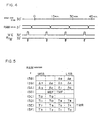
- Figure 5 is a chart showing positions and addresses of counter flags related to address counters in RAM inside a microcomputer;
- Figure 6 (A) and (B), is flow chart representing address counters and formation of a variety of timings in this system.
- Figure 7 is a diagram showing a partial block diagram and positions and addresses of register flags related to channel selecting resisters of inside RAM;
- Figure 8 (A) and (B), is a flow chart showing the channel selecting operation of this system; and
- Figure 9 is a flow chart of the part which prohibits the automatic operation, when the channel is identical with that which has been received by this system just before.
- A programmable channel selecting system for television sets embodying this invention is described hereunder with reference'to accompanying drawings:
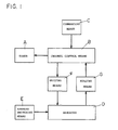
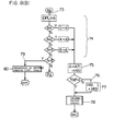
- First, Figure 1 shows the construction of this system by utilizing function blocks. Referring to this diagram, (A) designates a tuner for selecting the channel of television broadcasting to receive and (B) a channel control means for producing control signals to be impressed on the tuner (A) for controlling the channel selection. This channel control means (B) includes a remote control signal producing means which makes use of a microcomputer and a tuner control means for controlling the tuner by the remote control signals.
- The letter (C) designates a commanding means including a keyboard which is actually operated by the user at the time of manual switching, for entering into the channel control means (B) the channel data which represent the channels to select, in order to make manual switchings for the channel selection by the tuner.
- Further, (D) represents a memory for storing for one week, for example, program data available at 15 minutes intervals, for example, for automatic switching to be done by the program between channels through selection by the aforementioned tuner (A). For example, 672 types of address are provided in the memories.
- The letter (E) gives an address switching means for specifying write/read addresses in the aforementioned memories (D) by making switchings at such definite time intervals as, for example, 15-minutes and making the address designations with certain period cycles; (F) a writing means for taking out of the channel controlling means (B) the channel data which were entered by the commanding means (C) at the aforementioned manual switching times and which represent the channels that have been selected by the tuner through the channel controlling means (B) and, then, writing them as program data in the memories (D) at the addresses specified at those times to store them there, and (G) a reading means for reading out of the memories (D) the aforementioned program data at definite time intervals, at read times every hour, for example, 0, 15, 30 and 45 minutes and automatically switching between channels through selection by the tuner (A) on the basis of the aforementioned program data by entering the channel data into the channel controlling means (B) on the basis of the program data.
- These address switching means (E), writing means (F) and reading means (G) should be run by means of a microcomputer used in the channel controlling means (B).
- As above-described, in this system, the channel to select is automatically switched in accordance with the program by controlling with a remote control the channel to select by the tuner and controlling the remote controlling means installed inside the channel controlling means (B) by means of the program data read out of the memories (D). On the other hand, memories (D) for switching write/read address with a definite cycle (called step time) are used as the memories for storing program data. This step time is set at 15 minutes in this instance, so that the switchings take place at 0, 15, 30 and 45 minutes every hour. The address designations in the memories (D) are to be repeated with 1 week as one cycle. The timing relationships between the times for reset of addresses, switching of addresses, read, write and write permission in the memories (D) for programming are very important.
- In particularly describing the aforementioned example, the timings for read from the memories (D) shall be set at 0, 15, 30 and 45 minutes every hour. Since the step time is 15 minutes as above-described, the memory read times must exactly coincide with any of the times above-mentioned at the address reset times.
- Since, generally, the manual channel switching operations of a television set in use are thought to occur concentrically around the read times, for the broadcasting programs change at either 0, 15, 30 or 45 minutes every hour, the data are once written in the channel selecting registers in RAM in the microcomputer for remote control and, thereafter, the final channels selected are written in the memories (D). Accordingly, if channels have been manually switched many times around the read times, for example, each 5 minutes write permissive time, the channel selecting data will be renewed in the channel selecting registers one after another. After the write permissive times have ended, the data in the channel selecting registers will be written in the memories (D) for programming.
- On the other hand, the switching between addresses needs to be done before reading, but if no channel selecting register is provided, it needs to be done before the write permissive time (thus, 5 minutes before read time).
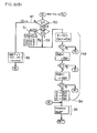
- Figure 2 is a block diagram showing an embodiment of this invention. The
numeral 1 denotes a microcomputer; 2 programmable memories comprising 4 1K but RAMs; 3, 3' and 3" address output latches; 4 a latch for delivery of WE (write enable) signal and write/read signals; 5 I/0 port; and 6 internal bus line. The numeral 7 designates a quartz oscillator for clock; 8, clock oscillator; 9, clock divider; 10, counter; 11, ALU; 12 accumulator; 13, register stack pointer; 14 RAM; 15, program counter; 16, ROM; 17, instruction decoder; 18, output latch; 19, input port; 20, keyboard; 21, input port; 22, mode changeover switch; 23, reset switch; 24, output port; 25, amplifier for remote control signal; and 26, infrared diode for delivery of remote control signal. Elements inside the dashed line are located on the chip of themicrocomputer 1. The power source is not shown in this diagram. Thenumeral 28 stands for a photo-diode for receiving the remote control signal; 29, tuner; and 28', a control circuit for controlling the tuner's (29) channel selection by the remote control signal. - Referring to Figure 2, when the
mode changeover switch 22 is opened to provide the write mode, akeyboard 20 as the commanding means (C) is a keyboard for channel command by the manually operated remote control; by specifying the channel by operating one of the keys, a pulse code row of the types corresponding to the respective channels to select is produced inside themicrocomputer 1, is, then, delivered from the output port 24 to theamplifier 25 for remote control signal, thereby making the operation of delivering infrared remote control signals by driving adiode 26. As this remote control signal is received by thephototransistor 28 and given to the tuner control circuit 28', the channel designated for actual entrance at that time by the command from thekeyboard 20 is selected by thetuner 29. The arrangement of elements to this tuner control circuit 28' is included in the channel controlling means (B) in Figure 1. - On the other hand, the output from the
clock oscillator 8 is divided by thedivider 9 andcounter 10, to allow offerings to occur every 0.5 seconds. - By making use of the offerings, timing signals are produced on a software basis inside the
microcomputer 1. Now, assuming that the offering occur every 0.5 seconds, that the step time for address switching by the address switching means E is 15 minutes and that the 1 cycle time for addresses in the memories is 7 days, the last channel selection data within the write permissive times, or 5 minutes before and after the read times, are written in thememories 2. The writing into thememories 2 shall be made immediately after ending the write permissive time and the address switching timing shall be just before ending the write permissive time. - The timing relationships at these times are shown in the time chart in Figure 3.
- The
numeral 30 represents the read times synchronized with the real times, which may be set in agreement with the latter by depressing thereset switch 23 at correct times: 0,15,30 and 45 minutes. Thenumeral 31 in Figure 3 gives the memories address signal; and 32 WE (write enable) signal ofmemories 2; when this signal is "1", the writing operation is enabled. Thenumeral 33 signifies R/W (read/write) signal, which, when rising from "0" to "1", writes the signal on the data bus into theaforementioned memory 2. The signal of 34 has represented by "1" the time range for writing the channel selecting data into the channel selecting register (which will be described later; refer to Figure 7) inside the microcomputer. The narrower the range, the more properly may the will of the operator be reflected. Too narrow a range, however, may result in lost data. If it is widened forwardly, the data'entered one step before may be mixed in. If it is widened backwardly, the result of selection will be reflected stronger. However, this merely indicates one direction of selection. - Figure 5 is a table showing the arrangement of address switching counters laid out in part of
RAM 14 inside themicrocomputer 1 and their addresses. - Figure 6 (A) and (B), is a flow-chart showing their operation. To- T11 in Figure 5 represent 12 bit counters which count 600 input signals at 0.5 second intervals on a software basis for a time length of 5 minutes. T12 and T13 stand for 2 bit counters, which count 3 5-minute inputs for the total of 15 minutes. TMF indicates a timer mode flag, which will be set to "1", when the
mode changeover switch 22 in Figure 2 is switched to Auto mode (a mode in which automatic channel selection is made, based on the channel selecting data from RAM, as the read time has arrived), but to "0", when it is switched to Man mode (a mode in which automatic channel selection is prohibited). WEF denotes a flag which gives "1", when thewrite time signal 34 in Figure 2 gives "1". Ao-A9 show address counters, which count 672 addresses for 7 days at 15 minute steps. - In the flow chart of Figure 6 (A), 40 designates the start of offerings by the timers, which occur every 0.5 seconds. As a timer offering has occurred, first, each present register is evacuated (41) and 5 minute counters 42 (
addresses 5F-5D) are raised by one count. This system is constructed on a software basis such that the 5 minute counters 42 are reset, after taking 600 counts (43). - As the 5 minute counters have been reset, a 15
minute counter 44 will be raised by one count. When the 15 minute counter has counted 5 minutes (45), WEF will be reset and WE output and R/W output will be produced (46). TMR1 and TMR2 signify timers formed on a software basis. - Subsequently, the steps of Figure 6 (B) are taken. Thus when the 15 minute timer has recorded 10 minutes (47), WEF will be set and the numbers counted in the address counters 48 will be delivered at address output latches 3, 3' and 3" (49). When the 15 minute timer has run 15 minutes (50) and the mode changeover switch is under Auto mode (51), channel selection signals are produced (52). When the mode switch is under Man (53), the channel selection signals will not be issued. Then the address counters 48 will be raised by one count. As the address counters 48 have taken 672 counts, they will be reset (54).
- On the whole returning route from the aforementioned operations, the initially evacuated registers will be returned (55), the offerings completed and the former program resumed.
- In the foregoing, the designs of counters' operations and formation of timings have been described.
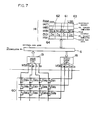
- In the following, the flow of channel selecting data is described: Figure 7 is a block diagram showing how the channel selecting data are taken in and Figure 8, (A) and (B), gives a flow chart showing the operation. Switches SWI-SW12 in Figure 7 designate a channel selection button group, by which "1 -"C" in hexadecimal notation in correspondence with the switches SW1-SW12 are written as channel number data in channel number registers 61. Scan counters 62 perform scanning of keys by successively turning to "1" each one of bits of
output latch 18. The circuits of Figure 7, exclusive of thekeyboard 60, are all placed on the chip of themicrocomputer 1. The numeral 14 represents RAM and 19 input port. These elements andALU 11 andaccumulator 12 are connected through abus 6. - The flow chart of Figure 8, (A) and (B), in contrast to that of Figure 6, (A) and (B), which is operated by offerings, is composed as part of a whole program loop. In this chart, such detail parts as a chattering preventer, etc., are not included. The numeral 65 represents a program for always making only one bit in the
output latch 18 "1", the highest level bit only remaining, when a plurality of bits are "1", but the lowest level bit giving "1", when all bits are "0". Then this signal is delivered from theoutput latch 18 by the step of 66, while the signal from theinput port 19 is taken into the accumulator 12 (67). - . If there is no input (or when not a key has been depressed) (68), the
scan counter 62 will be shifted by one place to left (69), then the program proceeding to the next step. When inputs have been made (70), the input values "1", "2", "4" and "8" (binary coded numbers) from theinput port 19, respectively, are converted into "1", "2", "3" and "4" (decimally coded numbers) which are, then, written into temporary memories 63 (71). If a plurality of inputs have been made, they will be returned through a loop of (72) and data will be again taken in (67). - After entering inputs into temporary memories 63 (73), the data in the
output latch 18 is judged and "0", "4" and "8" are put in the accumulator 12 (74) in correspondence with the data from theoutput latch 18, "1", "2" and "4", and with the content of thetemporary memory 63 added, are received in the channel number registers 61 (75). If the mode is Man (76), this data will be written in the channel selection registers (77). In accordance with this data, channel selecting signals will be delivered (78). When the data of theoutput latch 18 above-mentioned is 8 (79), this means that keys other than those for channel selection have been depressed; the flow will be branched to other remote control treatments (80). In this way, the expected operation may be performed with the circuit composition of Figure 2. - Besides, this system may be so arranged that when, the channel selection data from RAM during the read time shown in Figure 6 (B) and the data of the channel number registers 61 are in agreement, as compared in Figure 9 (56), the channel selecting operation will not be run.
- Or-it-may be composed such that the channel selecting data may be obtained which can be programmed only when same channels have been received continuously over n weeks, by adding to the program RAM such a judgement bit as effectively enters the channel selecting data into the addresses specified in the memories, only when such channel selecting data are entered that select same channels to same addresses over n cycles (n is an integer of 2 or more) of the address designation in the memories, for example, over n weeks.
- As described in the foregoing, the programmable channel selecting system of this invention enables program input of channel selection to be made under almost natural operating condition, obviating special program entering operation. Accordingly, this invention can provide a programmable channel selecting system which is optimally useful, as used in television or radio receivers.
- The following is a

Claims (3)
Applications Claiming Priority (2)
| Application Number | Priority Date | Filing Date | Title |
|---|---|---|---|
| JP57065897A JPS58182326A (en) | 1982-04-19 | 1982-04-19 | Program memory device |
| JP65897/82 | 1982-04-19 |
Publications (3)
| Publication Number | Publication Date |
|---|---|
| EP0105932A1 EP0105932A1 (en) | 1984-04-25 |
| EP0105932A4 EP0105932A4 (en) | 1985-04-11 |
| EP0105932B1 true EP0105932B1 (en) | 1987-11-25 |
Family
ID=13300211
Family Applications (1)
| Application Number | Title | Priority Date | Filing Date |
|---|---|---|---|
| EP83901227A Expired EP0105932B1 (en) | 1982-04-19 | 1983-04-15 | Program-selecting device |
Country Status (5)
| Country | Link |
|---|---|
| US (1) | US4593414A (en) |
| EP (1) | EP0105932B1 (en) |
| JP (1) | JPS58182326A (en) |
| DE (1) | DE3374748D1 (en) |
| WO (1) | WO1983003726A1 (en) |
Families Citing this family (39)
| Publication number | Priority date | Publication date | Assignee | Title |
|---|---|---|---|---|
| CH655587B (en) * | 1983-09-22 | 1986-04-30 | ||
| JPH06103507B2 (en) * | 1984-11-02 | 1994-12-14 | 株式会社日立製作所 | Pulse input / output processor and microcomputer using the same |
| US5089955A (en) * | 1984-11-02 | 1992-02-18 | Hitachi, Ltd. | Programmable counter/timer device with programmable registers having programmable functions |
| DE3524270A1 (en) * | 1985-07-06 | 1987-01-08 | Thomson Brandt Gmbh | DEVICE FOR AUTOMATICALLY SWITCHING ON AND OFF THE RECORDING OPERATION OF A VIDEO RECORDER |
| GB2192320B (en) * | 1986-06-27 | 1990-07-04 | Samsung Electronics Co Ltd | Video signal processing system for double deck video tape recorder |
| US4984295A (en) * | 1987-01-07 | 1991-01-08 | Motorola, Inc. | Programmable electronic device |
| GB8702187D0 (en) * | 1987-01-31 | 1987-03-04 | Long A T | Controlling video recorders |
| JP2511040B2 (en) * | 1987-06-02 | 1996-06-26 | 株式会社東芝 | Tuning device |
| DE3733015A1 (en) * | 1987-09-30 | 1989-04-20 | Thomson Brandt Gmbh | PROGRAMMING METHOD AND / OR DEVICE FOR AUDIO OR VIDEO DEVICES |
| JPH01155722A (en) * | 1987-12-11 | 1989-06-19 | Sony Corp | Receiver |
| JPH01168124A (en) * | 1987-12-23 | 1989-07-03 | Pioneer Electron Corp | Channel selection system for tuner |
| JPH01236826A (en) * | 1988-03-17 | 1989-09-21 | Toyo Commun Equip Co Ltd | Automatic channel selection device for television receiver and the like |
| CA2005070C (en) * | 1988-12-23 | 1999-04-27 | Henry C. Yuen | Apparatus and method for using encoded video recorder/player timer preprogramming information |
| US5974222A (en) * | 1988-12-23 | 1999-10-26 | Gemstar Development Corporation | Apparatus and method using compressed codes for scheduling broadcast information recording |
| US6049652A (en) * | 1988-12-23 | 2000-04-11 | Gemstar Development Corporation | Apparatus and method using compressed codes for recorder preprogramming |
| US6430359B1 (en) | 1988-12-23 | 2002-08-06 | Gemstar Development Corporation | Apparatus and method using compressed codes for television program record scheduling |
| US5307173A (en) * | 1988-12-23 | 1994-04-26 | Gemstar Development Corporation | Apparatus and method using compressed codes for television program record scheduling |
| JPH02252184A (en) * | 1989-03-24 | 1990-10-09 | Hashimoto Corp | Automatically selective viewing and hearing device for television and radio or the like |
| JPH03121628A (en) * | 1989-10-05 | 1991-05-23 | Hitachi Denshi Ltd | Automatic adjustment radio equipment |
| JPH0461510A (en) * | 1990-06-29 | 1992-02-27 | Matsushita Electric Ind Co Ltd | Channel selection device |
| AU2515295A (en) | 1994-05-16 | 1995-12-05 | Roy J. Mankovitz | Television program record scheduling and satellite receiver control using compressed codes |
| US5574494A (en) * | 1994-05-31 | 1996-11-12 | U.S. West Technologies, Inc. | Method for automatically navigating a complex struture at an interactive user station |
| US6769128B1 (en) | 1995-06-07 | 2004-07-27 | United Video Properties, Inc. | Electronic television program guide schedule system and method with data feed access |
| AU733993B2 (en) | 1997-07-21 | 2001-05-31 | Rovi Guides, Inc. | Systems and methods for displaying and recording control interfaces |
| US6476947B1 (en) * | 1998-05-04 | 2002-11-05 | Michael Lee Harvey | Process and apparatus for maximizing a software component and minimizing a hardware component of an infrared code |
| CN1867068A (en) | 1998-07-14 | 2006-11-22 | 联合视频制品公司 | Client-server based interactive television program guide system with remote server recording |
| US6898762B2 (en) | 1998-08-21 | 2005-05-24 | United Video Properties, Inc. | Client-server electronic program guide |
| US6792197B1 (en) | 1998-12-07 | 2004-09-14 | Index Systems, Inc. | System and method for generating video taping reminders |
| CA2425479C (en) | 2000-10-11 | 2014-12-23 | United Video Properties, Inc. | Systems and methods for providing storage of data on servers in an on-demand media delivery system |
| US7493646B2 (en) | 2003-01-30 | 2009-02-17 | United Video Properties, Inc. | Interactive television systems with digital video recording and adjustable reminders |
| US8438601B2 (en) | 2003-07-02 | 2013-05-07 | Rovi Solutions Corporation | Resource management for a networked personal video recording system |
| US7454120B2 (en) | 2003-07-02 | 2008-11-18 | Macrovision Corporation | Methods and apparatus for client aggregation of television programming in a networked personal video recording system |
| US8806533B1 (en) | 2004-10-08 | 2014-08-12 | United Video Properties, Inc. | System and method for using television information codes |
| JP4600203B2 (en) * | 2005-08-08 | 2010-12-15 | 株式会社日立製作所 | Video playback device |
| US8582946B2 (en) | 2005-11-04 | 2013-11-12 | Rovi Guides, Inc. | Systems and methods for recording programs using a network recording device as supplemental storage |
| US7801888B2 (en) | 2007-03-09 | 2010-09-21 | Microsoft Corporation | Media content search results ranked by popularity |
| US8293714B2 (en) * | 2008-05-05 | 2012-10-23 | Covx Technology Ireland, Ltd. | Anti-angiogenic compounds |
| US10063934B2 (en) | 2008-11-25 | 2018-08-28 | Rovi Technologies Corporation | Reducing unicast session duration with restart TV |
| US8805418B2 (en) | 2011-12-23 | 2014-08-12 | United Video Properties, Inc. | Methods and systems for performing actions based on location-based rules |
Family Cites Families (10)
| Publication number | Priority date | Publication date | Assignee | Title |
|---|---|---|---|---|
| JPS5346408B2 (en) * | 1973-03-19 | 1978-12-13 | ||
| DE2624733A1 (en) * | 1976-06-02 | 1977-12-15 | Droesel Hermann Dipl Math | Microprocessor based controller with learning capability - enamines input output status during step sequencing through cycle and data is entered into memory |
| JPS5346408A (en) * | 1976-10-08 | 1978-04-26 | Kawasaki Steel Co | Method of repairing furnace body cooler for shaft furnace |
| US4162513A (en) * | 1977-09-30 | 1979-07-24 | Rca Corporation | Television system scheduler |
| JPS6040741B2 (en) * | 1977-12-19 | 1985-09-12 | 松下電器産業株式会社 | Receiver with timer |
| US4228543A (en) * | 1978-03-24 | 1980-10-14 | Jackson Joseph N | Programmable television receiver controllers |
| JPS5527729A (en) * | 1978-08-17 | 1980-02-28 | Matsushita Electric Ind Co Ltd | Channel selection device |
| US4344000A (en) * | 1979-03-21 | 1982-08-10 | Dynascan Corporation | Power circuit control programmable timer |
| US4349748A (en) * | 1979-03-21 | 1982-09-14 | Dynascan Corporation | Timer and power control system |
| DE3023199C2 (en) * | 1980-06-21 | 1983-02-17 | Standard Elektrik Lorenz Ag, 7000 Stuttgart | Consumer electronics device with a programming device for preselected radio and / or television programs |
-
1982
- 1982-04-19 JP JP57065897A patent/JPS58182326A/en active Pending
-
1983
- 1983-04-15 WO PCT/JP1983/000120 patent/WO1983003726A1/en active IP Right Grant
- 1983-04-15 DE DE8383901227T patent/DE3374748D1/en not_active Expired
- 1983-04-15 US US06/568,240 patent/US4593414A/en not_active Expired - Fee Related
- 1983-04-15 EP EP83901227A patent/EP0105932B1/en not_active Expired
Also Published As
| Publication number | Publication date |
|---|---|
| JPS58182326A (en) | 1983-10-25 |
| US4593414A (en) | 1986-06-03 |
| DE3374748D1 (en) | 1988-01-07 |
| EP0105932A1 (en) | 1984-04-25 |
| WO1983003726A1 (en) | 1983-10-27 |
| EP0105932A4 (en) | 1985-04-11 |
Similar Documents
| Publication | Publication Date | Title |
|---|---|---|
| EP0105932B1 (en) | Program-selecting device | |
| US4081754A (en) | Programmable television receiver controllers | |
| US4162513A (en) | Television system scheduler | |
| US4004085A (en) | Receiving program-presetting system for a television receiver | |
| US5523781A (en) | System for controlling television and billing for its use | |
| US4620229A (en) | Picture display device | |
| EP0068422B2 (en) | Equipment for the reproduction of alphanumerical data | |
| GB2077069A (en) | Broadcast receiver with search tuning | |
| GB2063600A (en) | Receiver with a channel swapping apparatus | |
| GB1581525A (en) | Frequency synthesis control system | |
| US4379946A (en) | Signalling system and signal control equipment for multi-address calling | |
| GB1567052A (en) | Tuning circuits for communications receiving apparatus | |
| US4232301A (en) | Apparatus for automatically selectively displaying information of a plurality of kinds | |
| US4131853A (en) | Electronic multiple channel tuner | |
| US4031470A (en) | Operation program-presetting system | |
| EP0401849B1 (en) | Apparatus for referring to a content of a dial memory in a telephone set | |
| JPS5816646B2 (en) | Television electronic tuning device | |
| US4298851A (en) | Presettable tuning apparatus | |
| US5301106A (en) | Action item docketing device | |
| US4005368A (en) | Memory tuning system with automatic two speed display | |
| US4075422A (en) | Automatic page selectors | |
| US4063071A (en) | Flexitime recorder | |
| US4517683A (en) | Microprocessor controlled system for decoding serial data into parallel data for execution | |
| US4060768A (en) | Memory tuning system with dual speed programming | |
| JPS6352514B2 (en) |
Legal Events
| Date | Code | Title | Description |
|---|---|---|---|
| PUAI | Public reference made under article 153(3) epc to a published international application that has entered the european phase |
Free format text: ORIGINAL CODE: 0009012 |
|
| 17P | Request for examination filed |
Effective date: 19831222 |
|
| AK | Designated contracting states |
Designated state(s): DE FR GB |
|
| 17Q | First examination report despatched |
Effective date: 19860423 |
|
| GRAA | (expected) grant |
Free format text: ORIGINAL CODE: 0009210 |
|
| AK | Designated contracting states |
Kind code of ref document: B1 Designated state(s): DE FR GB |
|
| REF | Corresponds to: |
Ref document number: 3374748 Country of ref document: DE Date of ref document: 19880107 |
|
| ET | Fr: translation filed | ||
| PLBE | No opposition filed within time limit |
Free format text: ORIGINAL CODE: 0009261 |
|
| STAA | Information on the status of an ep patent application or granted ep patent |
Free format text: STATUS: NO OPPOSITION FILED WITHIN TIME LIMIT |
|
| 26N | No opposition filed | ||
| REG | Reference to a national code |
Ref country code: GB Ref legal event code: 746 Effective date: 19951123 |
|
| REG | Reference to a national code |
Ref country code: FR Ref legal event code: D6 |
|
| PGFP | Annual fee paid to national office [announced via postgrant information from national office to epo] |
Ref country code: GB Payment date: 19970407 Year of fee payment: 15 |
|
| PGFP | Annual fee paid to national office [announced via postgrant information from national office to epo] |
Ref country code: FR Payment date: 19970409 Year of fee payment: 15 |
|
| PGFP | Annual fee paid to national office [announced via postgrant information from national office to epo] |
Ref country code: DE Payment date: 19970418 Year of fee payment: 15 |
|
| PG25 | Lapsed in a contracting state [announced via postgrant information from national office to epo] |
Ref country code: GB Free format text: LAPSE BECAUSE OF NON-PAYMENT OF DUE FEES Effective date: 19980415 |
|
| PG25 | Lapsed in a contracting state [announced via postgrant information from national office to epo] |
Ref country code: FR Free format text: THE PATENT HAS BEEN ANNULLED BY A DECISION OF A NATIONAL AUTHORITY Effective date: 19980430 |
|
| GBPC | Gb: european patent ceased through non-payment of renewal fee |
Effective date: 19980415 |
|
| PG25 | Lapsed in a contracting state [announced via postgrant information from national office to epo] |
Ref country code: DE Free format text: LAPSE BECAUSE OF NON-PAYMENT OF DUE FEES Effective date: 19990202 |
|
| REG | Reference to a national code |
Ref country code: FR Ref legal event code: ST |