EP0091824B1 - Receiving circuit for a data transmission system - Google Patents
Receiving circuit for a data transmission system Download PDFInfo
- Publication number
- EP0091824B1 EP0091824B1 EP83302054A EP83302054A EP0091824B1 EP 0091824 B1 EP0091824 B1 EP 0091824B1 EP 83302054 A EP83302054 A EP 83302054A EP 83302054 A EP83302054 A EP 83302054A EP 0091824 B1 EP0091824 B1 EP 0091824B1
- Authority
- EP
- European Patent Office
- Prior art keywords
- voltage
- transmission line
- receiving station
- signal components
- receiving
- Prior art date
- Legal status (The legal status is an assumption and is not a legal conclusion. Google has not performed a legal analysis and makes no representation as to the accuracy of the status listed.)
- Expired
Links
Images
Classifications
-
- H—ELECTRICITY
- H04—ELECTRIC COMMUNICATION TECHNIQUE
- H04B—TRANSMISSION
- H04B3/00—Line transmission systems
- H04B3/54—Systems for transmission via power distribution lines
- H04B3/56—Circuits for coupling, blocking, or by-passing of signals
-
- H—ELECTRICITY
- H04—ELECTRIC COMMUNICATION TECHNIQUE
- H04B—TRANSMISSION
- H04B3/00—Line transmission systems
- H04B3/54—Systems for transmission via power distribution lines
-
- H—ELECTRICITY
- H04—ELECTRIC COMMUNICATION TECHNIQUE
- H04B—TRANSMISSION
- H04B2203/00—Indexing scheme relating to line transmission systems
- H04B2203/54—Aspects of powerline communications not already covered by H04B3/54 and its subgroups
- H04B2203/5404—Methods of transmitting or receiving signals via power distribution lines
- H04B2203/5425—Methods of transmitting or receiving signals via power distribution lines improving S/N by matching impedance, noise reduction, gain control
-
- H—ELECTRICITY
- H04—ELECTRIC COMMUNICATION TECHNIQUE
- H04B—TRANSMISSION
- H04B2203/00—Indexing scheme relating to line transmission systems
- H04B2203/54—Aspects of powerline communications not already covered by H04B3/54 and its subgroups
- H04B2203/5429—Applications for powerline communications
- H04B2203/5433—Remote metering
-
- H—ELECTRICITY
- H04—ELECTRIC COMMUNICATION TECHNIQUE
- H04B—TRANSMISSION
- H04B2203/00—Indexing scheme relating to line transmission systems
- H04B2203/54—Aspects of powerline communications not already covered by H04B3/54 and its subgroups
- H04B2203/5462—Systems for power line communications
- H04B2203/5483—Systems for power line communications using coupling circuits
Description
- The present invention relates to a receiving station for a system in which data is transmitted over a transmission wiring or lines, and more particularly to a receiving station equipped with a receiving circuit capable of data detection regardless of variations in load impedance characteristics over the transmission wiring to which devices of various impedance characteristics are randomly connected.
- Fig. 1 of the accompanying drawings illustrates a general data transmission system comprising a transmitting station 1, a transmission wiring or
lines 2, aload 3, and a receiving station 4. Under normal conditions, the load on thetransmission wiring 2 is subjected to small variations. Therefore, the presence or absence of a signal can easily be detected by a voltage developed across a load impedance ZR' in the receiving station. - Power wiring transmission is often employed for reducing the system cost. With a variety of devices connected randomly to power wiring or lines, the level of detected signal voltages across the load impedance becomes quite small if

- With the foregoing prior difficulty in view, it is an object of the present invention to provide a receiving station capable of detecting data transmitted over transmission wiring in a data transmission system irrespective of variations in load impedance characteristics.
- There is disclosed in Patents Abstract of Japan.
Volume 3, No. 22 (E-93) of 24th Feb. 1979, page 76 (E93) (abstract of JP-A-54813 Tokyo Denryoku K.K) a data transmission system which comprises a transmitting station, a receiving station, and a transmission wiring connecting the receiving and transmitting stations, the receiving station having a receiving circuit for determining whether there is a signal over the transmission wiring with the aid of the sum of a current and a voltage on the transmission wiring. This summation is effected by a receiver which is coupled to receive separately the current and voltage components of the transmitted signal. - However, there is not disclosure whatsoever in this prior art of the manner in which these components are combined in order to provide a detection signal.
- According to the present invention there is provided a receiving station (14) for receiving data signals transmitted from a transmitting station (10) over a transmission line (12), the transmission line having a variable load impedance caused by one or more load devices (13) connected thereto, said receiving station including a data detection circuit comprising:
- current detector means (17) magnetically coupled to said transmission line (12) for detecting current signal components of said data signals,
- voltage detector means (15) directly coupled to said transmission line (12) for generating voltage signal components of said data signals, and
- means for generating an output signal by combining said current signal components and said voltage signal components,
- characterised in that said current detector means and said voltage detector means are connected in series and in that said generator means comprises output impedance means (ZR) for simultaneously receiving said current signal components and said voltage signal components of said data signal, said output signal comprising a voltage developed across the impedance means (ZR) from said current and voltage signal components of said data signals,
- whereby said output signal voltage is generated with a sufficient signal strength to be detectable irrespective of the impedance of the variable load impedance (ZL).
- Preferably, the voltage detector means includes a coil (15) in series between a portion of said transmission line (12) an said output impedance means (ZR) and said current detector means includes a core (17) magnetically coupled to said portion of said transmission line, said coil (15) being wound around said core (17).
- Preferably there is also provided capacitor means (16) in series with said coil (15) and forming a series resonant circuit therewith, said resonant circuit being tuned to selectively pass only said data signals.
- ' The invention is particularly applicable where the transmission line is a conventional A.C. power supply line and said load devices (13) are power utilization devices connected to said power supply line (12).
- The present invention will be better understood from the detailed description given hereinbelow and the accompanying drawings which are given by way of illustration only, and thus are not limitative of the present invention and wherein:
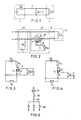
- Fig. 1 is an equivalent circuit diagram of a general data transmission system;
- Fig. 2 is a circuit diagram of a data transmission system according to an embodiment of the present invention;
- Fig. 3 is an equivalent circuit diagram of the arrangement in which the circuit of Fig. 2 is connected as shown by the solid line;
- Fig. 4 is an equivalent circuit diagram of the arrangement in which the circuit of Fig. 2 is connected as shown by the dotted line; and
- Fig. 5 is a system diagram showing an application in which the present invention is incorporated.
- Fig. 2 is a circuit diagram of a data transmission system including a transmitting station and a receiving station according to the present invention. The transmitting and receiving unit comprises a transmitting
station 10, areceiving station 14, a transmission wiring orlines 12, and aload 13. -
Coil 15 picks up a current flowing through thetransmission wiring 12 by way of coupling of magnetic fluxes. Thecoil 15 also serves to pick up a voltage by being connected to thetransmission wiring 12. Thecoil 15 is wound on an annular core 17 which is threaded by the transmission wiring. Acapacitor 16 and thecoils 15 constitute a series-connected resonance circuit. Thecapacitor 16 serves to pick up high frequency dependent on signals transmitted over thetransmission wiring 12 while rejecting other frequency components such as power supply frequencies (50/60 Hz). - The
coil 15 may be connected to thetransmission wiring 12 as shown by either the solid line A or the dotted line B. - Fig. 3 shows an equivalent circuit of the transmitting and receiving unit in which the circuit arrangement of Fig. 2 is connected as illustrated by the solid line A.
- A voltage VR across a load impedance ZR in the receiving station can be expressed by the following equation:

capacitor 16, and M the mutual inductance of the coils. - If the load impedance I ZR in the receiving station is selected to be higher than the impedances of the other components, the following expressions can be established in view of the fact that the coil L1 has a single turn and the coil L2 and the capacitor C causes series resonance with respect to a carrier frequency:

- By simplifying the equation (1) with the expressions (2) taken into account,

- When

- When

- Thus, when the effect of the load is small, the receiving station receives a voltage having substantially the same level as that of a transmitted voltage. When the effect of the load is large, a voltage dependent on the current flowing through the transmission wiring can be produced. Under ordinary conditions, a voltage can be obtained due to a combination of both of the load effects.
- Fig. 4 shows an equivalent circuit of the transmitting and receiving unit in which the circuit arrangement of Fig. 2 is connected as illustrated by the dotted line B.
- A voltage VR across the load imepdance ZR in the receiving station can be expressed by the following equation:

- With the inequalities (2) in view, the equation (6) becomes:

- As is apparent from the equation (3) or (7), the received voltage VR in the receiving station may be increased by:
- (i) making the impedance ZS as small as possible, and
- (ii) making the mutual inductance M as large as possible.
- The mutual inductance M is given by:

- (i) coupling the coils L1, L2 closely with each other (K-1), and
- (ii) increasing the inductance of the coil L2 (increasing the number of turns of the secondary winding).
- A power supply system for a single house in a multiple dwelling house is shown in Fig. 5. The power supply system has a watt-
hour meter 21, a main breaker 22, andsubbreakers 23 connected to various electric appliances. Where data is to be transmitted between houses in such a multiple dwelling house, the receiving circuit according to the present invention may be incorporated in a receiving station 24 (Fig. 5) for data reception without being affected by the impedance characteristics of the electric appliances in the house. - With the arrangement of the present invention, as described, the receiving station has a receiving circuit which is simultaneously capable of coupling of currents by way of magnetic coupling of coils and also of coupling of voltages by way of wiring connection. This allows data to be transmitted irrespectively of variations in the load impedance characteristics over transmission wiring to which devices of varying impedance characteristics are connected. A data transmission system with the receiving circuit of the invention is of particular advantage when used for power wiring data transmission characterized by a reduced system cost.
Claims (5)
Applications Claiming Priority (2)
| Application Number | Priority Date | Filing Date | Title |
|---|---|---|---|
| JP62785/82 | 1982-04-14 | ||
| JP57062785A JPS58179034A (en) | 1982-04-14 | 1982-04-14 | Data transmitting system |
Publications (3)
| Publication Number | Publication Date |
|---|---|
| EP0091824A2 EP0091824A2 (en) | 1983-10-19 |
| EP0091824A3 EP0091824A3 (en) | 1985-04-17 |
| EP0091824B1 true EP0091824B1 (en) | 1988-06-22 |
Family
ID=13210348
Family Applications (1)
| Application Number | Title | Priority Date | Filing Date |
|---|---|---|---|
| EP83302054A Expired EP0091824B1 (en) | 1982-04-14 | 1983-04-12 | Receiving circuit for a data transmission system |
Country Status (5)
| Country | Link |
|---|---|
| US (1) | US4622535A (en) |
| EP (1) | EP0091824B1 (en) |
| JP (1) | JPS58179034A (en) |
| CA (1) | CA1226919A (en) |
| DE (1) | DE3377189D1 (en) |
Families Citing this family (20)
| Publication number | Priority date | Publication date | Assignee | Title |
|---|---|---|---|---|
| US4823364A (en) * | 1987-03-12 | 1989-04-18 | The Boeing Company | Receive coupler for binary data communication systems |
| US4825450A (en) * | 1987-03-12 | 1989-04-25 | The Boeing Company | Binary data communication system |
| EP0302746B1 (en) * | 1987-08-07 | 1994-03-30 | Mitsui Petrochemical Industries, Ltd. | Apparatus for and method of discriminating signals |
| JPH06275979A (en) * | 1993-03-19 | 1994-09-30 | Nec Kansai Ltd | Structure for grounding high frequency unit |
| US5644286A (en) * | 1993-10-04 | 1997-07-01 | Lockheed Martin Corporation | Power bus digital communication system |
| WO1995029553A1 (en) * | 1994-04-25 | 1995-11-02 | Foster-Miller Inc. | Self-powered powerline sensor |
| DE19642034A1 (en) * | 1996-10-11 | 1998-04-23 | Gore W L & Ass Gmbh | Electrical data transmission device |
| US7158012B2 (en) | 1996-11-01 | 2007-01-02 | Foster-Miller, Inc. | Non-invasive powerline communications system |
| US5850114A (en) * | 1996-12-23 | 1998-12-15 | Froidevaux; Jean-Claude | Device for improving the quality of audio and/or video signals |
| US6677743B1 (en) | 1999-03-05 | 2004-01-13 | Foster-Miller, Inc. | High voltage powerline sensor with a plurality of voltage sensing devices |
| US6668058B2 (en) | 2000-03-07 | 2003-12-23 | Telkonet Communications, Inc. | Power line telephony exchange |
| US6975212B2 (en) * | 2001-10-02 | 2005-12-13 | Telkonet Communications, Inc. | Method and apparatus for attaching power line communications to customer premises |
| US7091831B2 (en) * | 2001-10-02 | 2006-08-15 | Telkonet Communications, Inc. | Method and apparatus for attaching power line communications to customer premises |
| US20040227623A1 (en) * | 2003-05-07 | 2004-11-18 | Telkonet, Inc. | Network topology and packet routing method using low voltage power wiring |
| US20040233928A1 (en) * | 2003-05-07 | 2004-11-25 | Telkonet, Inc. | Network topology and packet routing method using low voltage power wiring |
| US7493100B2 (en) | 2003-10-15 | 2009-02-17 | General Electric Company | Compensating for dynamic nulls in a power line communication system |
| US7548819B2 (en) * | 2004-02-27 | 2009-06-16 | Ultra Electronics Limited | Signal measurement and processing method and apparatus |
| US20060193336A1 (en) * | 2005-02-25 | 2006-08-31 | Telkonet, Inc. | Local area network above cable television methods and devices |
| US20060193310A1 (en) * | 2005-02-25 | 2006-08-31 | Telkonet, Inc. | Local area network above telephony methods and devices |
| US20060193313A1 (en) * | 2005-02-25 | 2006-08-31 | Telkonet, Inc. | Local area network above telephony infrastructure |
Family Cites Families (7)
| Publication number | Priority date | Publication date | Assignee | Title |
|---|---|---|---|---|
| JPS5129414B1 (en) * | 1970-04-03 | 1976-08-25 | ||
| US3986115A (en) * | 1975-01-20 | 1976-10-12 | The United States Of America As Represented By The Secretary Of The Navy | Transient direction detector |
| US4183072A (en) * | 1976-12-29 | 1980-01-08 | Mitsubishi Denki Kabushiki Kaisha | Protective relaying system |
| JPS586418B2 (en) * | 1977-06-03 | 1983-02-04 | 東京電力株式会社 | Signal reception method |
| US4281386A (en) * | 1979-08-01 | 1981-07-28 | Tokyo Shibaura Denki Kabushiki Kaisha | Systems for detecting faults in electric power systems |
| US4438396A (en) * | 1981-07-24 | 1984-03-20 | General Electric Company | Low cost volt/ampere meter with liquid crystal display |
| DE3262712D1 (en) * | 1982-01-18 | 1985-04-25 | Landis & Gyr Ag | Audiofrequency signals receiver |
-
1982
- 1982-04-14 JP JP57062785A patent/JPS58179034A/en active Granted
-
1983
- 1983-04-07 CA CA000425394A patent/CA1226919A/en not_active Expired
- 1983-04-08 US US06/483,252 patent/US4622535A/en not_active Expired - Lifetime
- 1983-04-12 EP EP83302054A patent/EP0091824B1/en not_active Expired
- 1983-04-12 DE DE8383302054T patent/DE3377189D1/en not_active Expired
Also Published As
| Publication number | Publication date |
|---|---|
| JPS6240894B2 (en) | 1987-08-31 |
| DE3377189D1 (en) | 1988-07-28 |
| JPS58179034A (en) | 1983-10-20 |
| EP0091824A3 (en) | 1985-04-17 |
| EP0091824A2 (en) | 1983-10-19 |
| CA1226919A (en) | 1987-09-15 |
| US4622535A (en) | 1986-11-11 |
Similar Documents
| Publication | Publication Date | Title |
|---|---|---|
| EP0091824B1 (en) | Receiving circuit for a data transmission system | |
| US4475209A (en) | Regenerator for an intrabundle power-line communication system | |
| AU595884B2 (en) | Power line communication interference preventing circuit | |
| KR950001370B1 (en) | Switch by-pass circuit | |
| US4504705A (en) | Receiving arrangements for audio frequency signals | |
| US3895370A (en) | High-frequency communication system using A-C utility lines | |
| US4254402A (en) | Transformer arrangement for coupling a communication signal to a three-phase power line | |
| US5257006A (en) | Method and apparatus for power line communications | |
| US4142178A (en) | High voltage signal coupler for a distribution network power line carrier communication system | |
| US4481501A (en) | Transformer arrangement for coupling a communication signal to a three-phase power line | |
| US3924223A (en) | Power line communication system having a protective terminating impedance arrangement | |
| US4621170A (en) | Means of transmitting signals along a line while also providing a direct voltage source | |
| US4646319A (en) | Bidirectional bus coupler presenting peak impedance at carrier frequency | |
| EP0124260A2 (en) | Power supply line carrier communication systems | |
| EP1500211B1 (en) | Adapter for communicating over power line | |
| EP0302746B1 (en) | Apparatus for and method of discriminating signals | |
| EP0098066B1 (en) | A data transmission system | |
| US3749857A (en) | Cable testing device for long-distance cables, particularly for occupied cables | |
| US4390863A (en) | System for the transmission of binary signals between the components of an alarm system | |
| US3909536A (en) | Audience survey system | |
| US1954794A (en) | Signaling system and electromagnetic mechanism therefor | |
| US1843525A (en) | Feeding arrangement for electric devices | |
| WO1996017444A1 (en) | Power line signalling system | |
| US2243180A (en) | All-wave radio receiving system | |
| JPS5975172A (en) | Transmitter and receiver driving circuit of sonnar |
Legal Events
| Date | Code | Title | Description |
|---|---|---|---|
| PUAI | Public reference made under article 153(3) epc to a published international application that has entered the european phase |
Free format text: ORIGINAL CODE: 0009012 |
|
| AK | Designated contracting states |
Designated state(s): DE FR GB IT |
|
| PUAL | Search report despatched |
Free format text: ORIGINAL CODE: 0009013 |
|
| AK | Designated contracting states |
Designated state(s): DE FR GB IT |
|
| 17P | Request for examination filed |
Effective date: 19850827 |
|
| 17Q | First examination report despatched |
Effective date: 19860917 |
|
| ITF | It: translation for a ep patent filed |
Owner name: DR. ING. A. RACHELI & C. |
|
| GRAA | (expected) grant |
Free format text: ORIGINAL CODE: 0009210 |
|
| AK | Designated contracting states |
Kind code of ref document: B1 Designated state(s): DE FR GB IT |
|
| REF | Corresponds to: |
Ref document number: 3377189 Country of ref document: DE Date of ref document: 19880728 |
|
| ET | Fr: translation filed | ||
| PLBE | No opposition filed within time limit |
Free format text: ORIGINAL CODE: 0009261 |
|
| STAA | Information on the status of an ep patent application or granted ep patent |
Free format text: STATUS: NO OPPOSITION FILED WITHIN TIME LIMIT |
|
| 26N | No opposition filed | ||
| ITTA | It: last paid annual fee | ||
| PGFP | Annual fee paid to national office [announced via postgrant information from national office to epo] |
Ref country code: GB Payment date: 19970403 Year of fee payment: 15 |
|
| PGFP | Annual fee paid to national office [announced via postgrant information from national office to epo] |
Ref country code: FR Payment date: 19970409 Year of fee payment: 15 |
|
| PGFP | Annual fee paid to national office [announced via postgrant information from national office to epo] |
Ref country code: DE Payment date: 19970418 Year of fee payment: 15 |
|
| PG25 | Lapsed in a contracting state [announced via postgrant information from national office to epo] |
Ref country code: GB Free format text: LAPSE BECAUSE OF NON-PAYMENT OF DUE FEES Effective date: 19980412 |
|
| PG25 | Lapsed in a contracting state [announced via postgrant information from national office to epo] |
Ref country code: FR Free format text: THE PATENT HAS BEEN ANNULLED BY A DECISION OF A NATIONAL AUTHORITY Effective date: 19980430 |
|
| GBPC | Gb: european patent ceased through non-payment of renewal fee |
Effective date: 19980412 |
|
| PG25 | Lapsed in a contracting state [announced via postgrant information from national office to epo] |
Ref country code: DE Free format text: LAPSE BECAUSE OF NON-PAYMENT OF DUE FEES Effective date: 19990202 |
|
| REG | Reference to a national code |
Ref country code: FR Ref legal event code: ST |