EP0091191B1 - Phase detector control for a servo system - Google Patents
Phase detector control for a servo system Download PDFInfo
- Publication number
- EP0091191B1 EP0091191B1 EP83301019A EP83301019A EP0091191B1 EP 0091191 B1 EP0091191 B1 EP 0091191B1 EP 83301019 A EP83301019 A EP 83301019A EP 83301019 A EP83301019 A EP 83301019A EP 0091191 B1 EP0091191 B1 EP 0091191B1
- Authority
- EP
- European Patent Office
- Prior art keywords
- signal
- counter
- microprocessor
- line
- movable member
- Prior art date
- Legal status (The legal status is an assumption and is not a legal conclusion. Google has not performed a legal analysis and makes no representation as to the accuracy of the status listed.)
- Expired
Links
Images


Classifications
-
- G—PHYSICS
- G11—INFORMATION STORAGE
- G11B—INFORMATION STORAGE BASED ON RELATIVE MOVEMENT BETWEEN RECORD CARRIER AND TRANSDUCER
- G11B15/00—Driving, starting or stopping record carriers of filamentary or web form; Driving both such record carriers and heads; Guiding such record carriers or containers therefor; Control thereof; Control of operating function
- G11B15/18—Driving; Starting; Stopping; Arrangements for control or regulation thereof
- G11B15/46—Controlling, regulating, or indicating speed
- G11B15/467—Controlling, regulating, or indicating speed in arrangements for recording or reproducing wherein both record carriers and heads are driven
-
- H—ELECTRICITY
- H02—GENERATION; CONVERSION OR DISTRIBUTION OF ELECTRIC POWER
- H02P—CONTROL OR REGULATION OF ELECTRIC MOTORS, ELECTRIC GENERATORS OR DYNAMO-ELECTRIC CONVERTERS; CONTROLLING TRANSFORMERS, REACTORS OR CHOKE COILS
- H02P23/00—Arrangements or methods for the control of AC motors characterised by a control method other than vector control
- H02P23/18—Controlling the angular speed together with angular position or phase
- H02P23/186—Controlling the angular speed together with angular position or phase of one shaft by controlling the prime mover
Definitions
- the present invention generally relates to servo systems and, more particularly, to a phase detection control of a variable in a servo system where the phase is discretely measured.
- the present invention is adapted to control a variable where the phase is discretely measured, such as a motor having a tachometer of an optical type, for example. More particularly, in the environment of the disclosure of the apparatus described herein, it is associated with a capstan servo of a recording and reproducing apparatus. Obviously, the apparatus of the present invention is adapted to detect the phase and control a drive motor for a rotatable member or of any other type of variable drive where the phase is discretely measured. Many prior art phase detection servo controlled systems are direction sensitive to the reference or to the measured feedback direction. Such systems are susceptible to running away if the control variable rate exceeds the reference rate in the reverse direction.
- a further object of the present invention is to provide a phase detection and servo control system of the foregoing type which automatically eliminates the possibility of reverse run away if the control variable rate exceeds the reference rate in the reverse direction.
- a preferred object of the present invention is to provide an improved phase detection control for a servo system of the foregoing type which accomplishes the foregoing objects simply and inexpensively due to its superior design which has relatively few circuit components.
- the servo apparatus known from GB-2012999A has features corresponding to those in the premable of claim 1.
- the invention provides servo apparatus for controlling the speed of a movable member, comprising means for providing a two-level reference signal having transitions between levels at a rate indicative of a desired speed of the movable member, means for providing a two-level feedback signal having transitions between levels at a rate indicative of the actual speed of the movable member, a phase difference between transitions of the reference signal and the feedback signal respectively being indicative of a difference between the speed of the movable member and the desired speed, a counter capable of counting clock pulses to provide a pulse count in accordance with the phase difference and drive means responsive to the pulse counter for adjusting the speed of the movable member, characterised by latches responsive to each clock pulse and the contemporaneous level of each signal to provide respective latched signal levels for the duration of a clock pulse period and a logic circuit, responsive to the latched levels and a direction signal which indicates the direction of movement of the movable member relative to a reference direction corresponding to a normal direction of movement of the member, the logic circuit enabling the
- phase detection control apparatus of the present invention is described in the environment of an apparatus which includes a microprocessor that effectively controls the major servo systems of a tape recording and reproducing apparatus, including servos which control the scanning drum operation, the automatic scan tracking, the reels and the capstan, the last of which includes the specific phase detection circuitry that embodies the present invention. Since the servos other than the capstan servo are not particularly relevant to the present invention, they are not described herein, but for a full and comprehensive description of the entire servo system, reference is made to our co-pending European Patent Application No. 83301016.8 filed 25th February 1983 (publication No. 0091188).
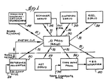
- a microprocessor 30 which is interconnected by a data bus 31 with a reel servo 32, a capstan servo 34, a scanner servo 36 and a machine communication interface and data 38 which essentially controls the various modes of the recording and reproducing apparatus as manipulated by an operator or from a remote location.
- the microprocessor also interacts with a reference generator 40 which receives as an input thereto a reference station composite sync signal via line 42 and the reference generator generates system clocks which clock the microprocessor and which in turn synchronizes all of the clock timing of the servos and other circuitry.
- the microprocessor also interacts with the automatic scan tracking servo 44 and a tape sync processor 46 which has a tape composite sync signal input via line 48.
- the tape sync processor additionally provides a signal to the time base corrector interface 50 which provides appropriate timing and control signals for use by the time base corrector to provide a broadcast quality video image having the requisite stability and vertical position with respect to system reference as well as the correct chroma information, which processing varies depending upon what reproducing mode the apparatus is being operated.
- FIG. 1 illustrates the interaction of the microprocessor with the various servo systems of the apparatus, with machine control and with the time base corrector and the like
- the system can also be functionally described in terms of input and output signals that are provided to and from the microprocessor and this functional block diagram is shown in Figure 2.
- the microprocessor 30 receives frequency, phase and timing data shown by the upper left functional block including such input signals as scanner tach pulses, reel tach pulses, capstan tach pulses, reference vertical and frame timing signals, which is converted into digital information for processing by the microprocessor.
- the microprocessor also receives analog information shown by the block left of the microprocessor which is converted into digital information for processing by the microprocessor and such analog input signals include the automatic scan tracking error signals, the tension arm error signals and various motor currents from the reel drive motors, the capstan drive motor and the scanner drive motor.
- the data bus also receives operating mode information as well as other machine control data and it processes this information and provides status information and other data.
- the microprocessor generates digital information which is converted to analog information and these analog output signals include control signals for the capstan servo, the reel servo, the scanner servo and the automatic scan tracking servo.
- the microprocessor provides frequency, phase and timing output information which include delay signals, phase and timing output information that are used by the various servos and other circuits.
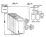
- the apparatus is programmed to operate in various operating modes as is shown in the broad flow chart of Figure 3a.
- the flow chart representing microprocessor software shows that once the machine is initialized, a mode is selected and these modes include stop, record, slow and fast motion reproduce, stop motion or still frame reproduce, ready and normal play.
- a mode test to determine if it is a valid mode and if such is the case, it will return to that mode and begin running the program that controls the apparatus in that mode. If the mode test is invalid, then it will return to the stop mode and the apparatus will stop. After the apparatus is placed in a valid mode, it will continue in that mode until some event occurs, such as a mode change or a completion of some operation.
- each operating mode includes various subroutines which are called as shown in Figure 3a. Certain ones of these subroutines are used in various ones of the operating modes.
- the play mode will contain a block of code instructions that will call up various subroutines in the specified order. As long as the apparatus is operating in the play mode it will repetitively go through this block of code instructions. When the scanner tachometer pulse occurs, it will cause an interrupt to the microprocessor as shown in Figure 3b.
- the microprocessor operates on an interrupt basis, with an interrupt resulting from one of three inputs.
- the software determines which input caused the interrupt and the microprocessor then enters the appropriate block of code which runs through various subroutines until it reaches the end and then returns to the instruction that had previously been completed prior to the interrupt.
- the scanner tachometer pulse originally triggered a counter which has a count that exceeds the maximum time required to store all current relevant information in stack registers in the microprocessor. When this is done, it is ready to immediately perform the instructions in the scanner 1 block of code. This is carried out by the scanner interrupt block of code which causes the microprocessor to store in the information and then literally wait for the scanner 1 interrupt. After the scanner 1 block of code is run, the microprocessor removes the information from the stack registers and resumes running through the instructions specified by the operating mode.
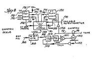
- the capstan servo is illustrated by the functional block diagram of the accompanying Figure 4.
- the tape 72 is controlled by the capstan 76 which has a drive motor 150 with an associated tachometer, the tachometer providing tachometer pulses on line 152 which provides an inner servo loop function.
- the tachometer signal is applied to an up/down counter 154 the output of which is applied to a digital-to-analog converter 156 via line 158 and its output is fed to a motor drive amplifier 160 that controls the motor 150.
- the up/down counter 154 also has an input line 162 provided by a 16-bit counter 164 which has as a reference frequency a 4 MHz signal applied thereto via line 166.
- the counter essentially controls the frequency of the reference signal that is applied to the up/down counter through its output line 162.
- the microprocessor 30 loads a number into the counter via line 168 which essentially controls the output frequency on line 162. Varying the number that is loaded into the counter 164 changes the division function to thereby vary the output reference signal frequency and thereby vary the speed of the capstan.
- the upper left hand portion of the block diagram illustrates the control track reference logic function which has inputs comprising the reference vertical information via line 170, the color framing information via line 172.
- control track play logic circuitry 186 provides a control track frame rate signal on line 188, 1/4 frame and 1/2 frame rate signals on lines 190 and 192, which signals are also applied to the microprocessor.
- the microprocessor determines whether the recorder must perform a color frame match operation.
- the apparatus If the apparatus is operating as a 525 line NTSC recording and reproducing apparatus, it will color frame match using the 1/2 frame rate signal and if it is operating as a 625 line PAL or SECAM system, it will color frame match using the 1/4 rate signal.
- the control track play logic therefore is adapted to control the tape so that proper color framing is achieved.
- variable control potentiometer 196 on the front panel of the recorder which controls the capstan and therefore the tape speed.
- the variable control signal is converted from analog to digital form for use by the microprocessor, which could be done by the analog-to-digital converter shown in Figures 5a and 5b if desired.
- the digital variable control signal is applied to the microprocessor when then applies a corresponding digital word to the counter 164 for controlling the speed.
- the control is non- linearized and programmable to provide nonlinear control of capstan speed as a function of the potentiometer position and the actual tape speed.
- microprocessor circuitry The microprocessor circuitry
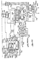
- the microprocessor 30, which is a Motorola integrated circuit Model MC 6802 has 16 address lines which address circuit components as well as specific addresses of memory circuits.
- address lines A o through A ls extend rightwardly to a random access memory 280 which is controlled by address lines A o through A 7 , as well as respective programmable read only memories 282 and 284 ( Figure 5b) which are controlled by address lines A o through All.
- the address lines also extend to a buffer 286 which has output lines indicated generally at 288 which extend to the second printed circuit board address lines.
- the lines 288 also extend downwardly to respective decoder integrated circuits 290 and 292 which are used to select ports P o through P ⁇ o .
- the address lines also extend to yet another decoder 294 which provides selection of various programmable timer integrated circuits T " through T H .
- Decoders 290, 292 and 294 are enabled when a master decode enable line S 4 is active and this is provided by a master decode circuit 296 located to the left of the decoder 294.
- address lines A 12 , A 13 and A 14 from the microprocessor 30 control the address selection master decode enable output lines So through S 7 that activate various portions of the circuitry.
- the decoded output line So enables the random access memory 280
- decode output S 6 enables the memory 282
- the decode output S 7 similarly enables memory 284.
- the data bus 31 from the microprocessor comprises eight output lines Do through D 7 extending to the memories 280, 282, 284 as well as to bidirectional buffers 298 and 300.
- Buffer 290 has output lines that extend the data bus to the second printed circuit board, and it is activated by the decode output S 5 . Activation of the decode output S 4 enables the decoders 290, 292 and 294 as well as the other bidirectional buffer 300 which effectively extends the data bus to the remaining circuitry shown in the upper portion of Figures 5a and 5b and to remaining circuitry on board No. 1.
- the data bus 31 has input latches 302 and 304 connected thereto and an output latch 306 being shown in Figure 5b.
- the data lines 308 are also connected to these latches and the lines 308 represent a data bus to the machine control system which has a separate microprocessor controlled system for carrying out other machine control functions of the apparatus independently of the system controlled by microprocessor 30.
- the interaction of operator control and mode switches, diagnostics and the like with the servo system of the present invention is carried out through this data bus via the latches 302, 304 and 306.
- latches are respectively enabled by enable lines E o , E 1 and E 2 which are decoded outputs of a decoder circuit 310 that has operator activated address lines A o through A3 from the machine control system.
- the decode circuit 310 is enabled by a line 312 from the machine control system.
- a latch 314 that is connected to the data bus can receive a data word which decodes an address for controlling a multiplexing.
- switch 316 selects one of the left inputs thereof for application onto line 318 that extends to an analog-to-digital converter, indicated generally at 320, having output lines 322 which extend to a latch 324 which applies data onto the data bus for use by the microprocessor when a port line P o is enabled from the address decoder 292.
- the multiplexing switch 316 can select a capstan servo control track error signal applied via line 326, an automatic scan tracking movable element position error signal applied via line 328 or a signal that is indicative of the position of the tension arm 70 applied via line 330.
- the circuitry at the upper portion of Figure 5a provides an analog signal on line 330 that represents the position of the previously described arm through appropriate loop compensation circuitry indicated generally at 331.
- the arm positional reference for forward and reverse arm locations during shuttle and still frame reproducing is set by coding lines 333 and 335 by means of the output latch 314 from the microprocessor.
- line 337 can be selected to measure the actual mechanical arm position for tape threading and unthreading.
- the capstan servo described in the block diagram of Figure 4 embodied by the detailed circuitry shown in Figures 6a and 6b.
- the capstan tachometer signal is applied on line 640 ( Figure 6b) which extends to a D latch which is part of the quad D latch integrated circuit 642 and the reference input frequency signal is applied via line 644.
- the latches are clocked by the microprocessor output clock E via line 646 and this clock also clocks an up/down counter 648, the output of which is applied to a digital-to-analog converter 650 which provides an analog output signal to the drive amplifier circuitry, indicated generally at 652.
- the circuitry includes a high gain section 654 and a low gain section 656 and a switching circuit 658 controlled by the microprocessor to either provide a high or low gain error signal.
- Line 660 controlled by the microprocessor, controls the switching circuit 658 to either apply the high gain signal from the upper circuitry 654 or the low gain signal from the lower circuitry 656 through the switcher onto line 662 which results in the capstan error signal being produced at the output line 664.
- the circuitry shown in Figure 6b effectively compares the phase of the reference on line 644 with the phase of the capstan tachometer on line 640 and provides a capstan servo error signal to control the precise speed of the capstan.
- the illustrated circuitry has the advantage that it does not suffer from common problems that can cause a servo system to run away in that it is incapable of doing so because of the absence of any capstan direction sensitivity or any upper or lower speed limits.
- the circuitry eliminates the possibility of reverse run away, even if the control variable rate, i.e., the capstan tachometer, exceeds the reference rate in the reverse direction. More specifically, common prior art capstan servos can run away in two different ways.
- the first can occur if the polarity of the feedback is reversed from that defined according to the normal capstan direction without a corresponding reversal of the generated error.
- the second way in which the capstan can run away occurs when the up/down counter is permitted to roll-over when the count limit conditions are reached.
- the circuitry uses the fully synchronous up/ down binary counter 648 and appropriate gating to enable the counter and to control an up/down control line 666.
- the reference input and tachometer inputs are automatically guided to increment or decrement the counter 648 in accordance with the direction lines.
- the output of the D latches for the capstan tachometer line 640 is applied to a NAND gate 668 and the reference signal is gated through the D latch and it is connected to an EXCLUSIVE OR gate 670.
- the NAND gate 668 provides a low output for every positive transition of the capstan tachometer pulse and this low output signal has a duration of one clock period.
- the reference signal that is applied through the D latch to the EXCLUSIVE OR gate 670 produces a low signal for every transition of the reference signal and this low signal also lasts for one clock period.
- the output from the EXCLUSIVE OR 670 is applied to an inverter 672, as well as to one input of another EXCLUSIVE OR gate 674, with the output of the inverter 672 being applied to a NAND gate 676.
- the NAND gate 668 output is applied to an inverter 678, as well as to the other input of the EXCLUSIVE OR gate 674.
- the output of the inverter 678 is applied to one input of a NAND gate 680 and the outputs of NAND gates 680 and 676 are applied to NAND gate 682, the output of which extends via an inverter 684 and line 666 to the up/down control of the up/down counter 648.
- the output of the EXCLUSIVE OR gate 674 is applied through an inverter 686 and line 688 to enable the input of the up/down counter 648.
- the operation of the logic circuitry is effective to control the up/down control line 666 so as to change the digital value of the counter in the proper direction to reduce the error. If the system contains no error, then the reference and capstan tachometer signals will be coincident and in such event, low outputs will be produced by the NAND gate 668 as well as the EXCLUSIVE OR gate 670 and both inputs will cause the EXCLUSIVE OR gate 674 to disable the up/down counter so that it will neither be incremented or decremented by the clock. If only one of the gates 668 or 670 is active, then the logic circuitry will cause the up/ down line to be controlled at the proper signal level so as to either increment or decrement the counter in the correct direction to reduce the error.
- the gate 680 also has one input supplied by a capstan forward and reverse control line 689 which automatically steers the logic to control the up/down control line so as to reduce the error regardless of the direction the capstan is being driven.
- the recorded control track information is used in the conventional manner and this operation is also accomplished under microprocessor control.
- the control track signal on input line 690 is applied through inverter 692 and EXCLUSIVE OR gate 694, whose output appears on line 696 which extends downwardly to an AND gate 698 (Figure 6b) that has its output line 700 applied to the input of a one-shot multivibrator 702 that is part of programmable timer chip 704.
- Line 700 also extends to clock a D flip-flop 706 ( Figure 6a) which has a Q output line 708 that clears a flip-flop 710 that provides a playback flag.
- the free-wheeling one-shot 702 has output line 712 that extends to the other input of the AND gate 698 and the AND gate and one-shot operate to block any spurious control track signals that may be present on line 696 until shortly before the control track pulse is expected to occur, at which time the free-wheeling one-shot changes state to enable the legitimate control track pulse to be applied and be gated through the AND gate 698 and again trigger the one-shot 702.
- the change of state of the free-wheeling one-shot 702 timing out will similarly cause an output signal on line 712 and the AND gate will provide a clock signal on line 700 to flip-flop 706 in the same manner as would an actual control track pulse.
- An output line 714 from flip-flop 706 is applied to the input of a flag sample gate counter 716 of a programmable timer chip 718 as well as a 1/2 ramp delay one-shot 720, the latter of which provides an output on line 722 which triggers a digital-to-analog converter 724 which samples the value of up/down counter 726 which contains the digital values of the control track signal.
- the 1/2 ramp delay 720 effectively causes the digital-to-analog converter 724 to sample the value of the counter 726 at the mid-point of the frame signal and properly times the control track playback signal. Stated in other words, the digital-to-analog converter 724 is triggered by the 1/2 ramp delay 720 so that the control track sample which is delayed from the actual control track by 1/2 ramp delay results in the actual control track and the actual reference being in phase.
- the capstan servo circuitry programmable timer chip 704 ( Figure 6a) reference vertical input signal on line 730 which is applied to a tracking one-shot 732.
- the tracking one-shot is programmed to directly follow the reference vertical and apply a pulse on output line 734 which is applied to a counter divider 736 that in turn provides various output signals, such as a frame rate signal on line 738, a 1/2 frame rate signal on line 740, and a 1/4 frame rate signal on line 742.
- the frame signals will be synchronized to reference vertical and is phase adjustable by operation of the control track phase control.
- the programmable timer chip 704 and particularly the tracking one-shot 732 therein in that it can be reprogrammed to operate as a rate generator and provide an output that varies slightly relative to the input reference.
- the output signal on line 734 may be one count in 40,000 counts different relative to the reference vertical or any other difference can be programmed by the microprocessor so that a definite time compression or expansion of the reproduction can be obtained if desired. This would permit an entire program to be speeded up or slowed down to fit the time slot that is desired and it can be done without removing any particular segment of the program. All that needs to be done is to reprogram the tracking one-shot section of the timer chip 704 to provide a time difference that will result in either a time expansion or compression of the program and all of the program content will still be present during reproducing.
- Figure 6b which has the reference vertical signal applied via input line 730 as previously described.
- the output of the one-shot 732 provides a delay time that is a function of a control track phase adjustment potentiometer which is located on the front panel of the apparatus and which is a part of the operator controlled machine control system.
- the output from the tracking one-shot 732 appears on line 734 to the divider 736 and the frame output on line 738 is used to control the up/down line of the counter 726 shown in Figure 6a.
- the value of the counter is latched into the digital-to-analog converter 724 by the control track playback frame pulse on line 722 which thereby generates a control track error voltage that appears at the output of the digital-to-analog converter 724 and which ultimately results in a signal at output line 326 that is one of the inputs to the analog-to-digital converter circuit 320 shown in Figure 5b.
- the circuitry of Figure 5b converts the analog value to an 8-bit word that is applied to the microprocessor 30 through the multiplexed analog-to-digital converter 320 shown in Figure 5b.
- the microprocessor converts the data to a 16- bit word which it applies to an inner loop reference counter 744 ( Figure 6b) which clocks a D flip-flop 746 that operates as a divide-by-two and provides the reference input signal on line 644 which closes the control track servo loop.
- the microprocessor 30 When the apparatus is operating in the asynchronous playback mode, the microprocessor 30 is programmed to write a high signal to a latch 748 which has an output line 750 that extends to gates 752 and 754 ( Figure 6b).
- the high signal on line 750 effectively disables the loading operations that would occur in the divider 736 and it additionally forces the input to the tracking one-shot 732 high to enable it to begin counting.
- the tracking one-shot is thereby changed to be a rate generator that produces an output vertical reference frequency that is programmable by the microprocessor. Since the output to the counter 732 is the studio reference clock frequency, the output can be programmed to be different from the normal reference vertical by the expression
- the programmed count can be derived from a local or a remote source.
- the automatic scan tracking head since the tape will be moving at a speed that is slighly different from the normal record or reproduce speed to accomplish the desired time compression or expansion, the automatic scan tracking head will occasionally be required to make a track jump. For this reason, the automatic scan tracking servo and time base corrector operation is switched from normal play to variable play so that the desired track jumps can be carried out.
- phase detector automatically compensates for the direction of the reference as well as the controlled variable.
Description
- The present invention generally relates to servo systems and, more particularly, to a phase detection control of a variable in a servo system where the phase is discretely measured.
- The present invention is adapted to control a variable where the phase is discretely measured, such as a motor having a tachometer of an optical type, for example. More particularly, in the environment of the disclosure of the apparatus described herein, it is associated with a capstan servo of a recording and reproducing apparatus. Obviously, the apparatus of the present invention is adapted to detect the phase and control a drive motor for a rotatable member or of any other type of variable drive where the phase is discretely measured. Many prior art phase detection servo controlled systems are direction sensitive to the reference or to the measured feedback direction. Such systems are susceptible to running away if the control variable rate exceeds the reference rate in the reverse direction.
- Accordingly, it is an object of the present invention to provide a phase detection servo control of such a variable which is incapable of running away due to any direction sensitivity of either the reference or the feedback or because of any upper or lower limits that are imposed by the circuitry.
- A further object of the present invention is to provide a phase detection and servo control system of the foregoing type which automatically eliminates the possibility of reverse run away if the control variable rate exceeds the reference rate in the reverse direction.
- A preferred object of the present invention is to provide an improved phase detection control for a servo system of the foregoing type which accomplishes the foregoing objects simply and inexpensively due to its superior design which has relatively few circuit components.
- The servo apparatus known from GB-2012999A has features corresponding to those in the premable of
claim 1. - The invention provides servo apparatus for controlling the speed of a movable member, comprising means for providing a two-level reference signal having transitions between levels at a rate indicative of a desired speed of the movable member, means for providing a two-level feedback signal having transitions between levels at a rate indicative of the actual speed of the movable member, a phase difference between transitions of the reference signal and the feedback signal respectively being indicative of a difference between the speed of the movable member and the desired speed, a counter capable of counting clock pulses to provide a pulse count in accordance with the phase difference and drive means responsive to the pulse counter for adjusting the speed of the movable member, characterised by latches responsive to each clock pulse and the contemporaneous level of each signal to provide respective latched signal levels for the duration of a clock pulse period and a logic circuit, responsive to the latched levels and a direction signal which indicates the direction of movement of the movable member relative to a reference direction corresponding to a normal direction of movement of the member, the logic circuit enabling the counter to count selectively up and down, the direction of count depending on the directional sense of the phase difference, when the said direction signal indicates that the direction of movement of the member is the same as the reference direction and controlling the counter to count in only one direction when the direction signal indicates that the direction of movement of the member is different from the reference direction.
-
- Figure 1 is a functional block diagram illustrating the functional interaction of a microprocessor with the various servo systems of the apparatus, and of the microprocessor and other important circuitry;
- Figure 2 is another functional block diagram of the microprocessor and illustrates the manner in which it receives input information relating to the operation of the apparatus and provides output signals that are used to control the operation of the apparatus;
- Figures 3a and 3b are very broad flow charts illustrating the software functional operation of the microprocessor;
- Figure 4 is a functional block diagram of the capstan servo system;
- Figures 5a and 5b together comprise a detailed electrical schematic diagram illustrating the microprocessor together with machine control interfacing circuitry and multiplexing analog-to-digital converting circuitry; and
- Figures 6a and 6b together comprise a detailed electrical circuit schematic diagram of the capstan servo circuitry of the apparatus, which detailed circuitry carries out the operation of the block shown in Figure 4.
- Broadly stated, the phase detection control apparatus of the present invention is described in the environment of an apparatus which includes a microprocessor that effectively controls the major servo systems of a tape recording and reproducing apparatus, including servos which control the scanning drum operation, the automatic scan tracking, the reels and the capstan, the last of which includes the specific phase detection circuitry that embodies the present invention. Since the servos other than the capstan servo are not particularly relevant to the present invention, they are not described herein, but for a full and comprehensive description of the entire servo system, reference is made to our co-pending European Patent Application No. 83301016.8 filed 25th February 1983 (publication No. 0091188).
- In block diagram of Figure 1 is shown a
microprocessor 30 which is interconnected by adata bus 31 with areel servo 32, acapstan servo 34, ascanner servo 36 and a machine communication interface anddata 38 which essentially controls the various modes of the recording and reproducing apparatus as manipulated by an operator or from a remote location. The microprocessor also interacts with areference generator 40 which receives as an input thereto a reference station composite sync signal vialine 42 and the reference generator generates system clocks which clock the microprocessor and which in turn synchronizes all of the clock timing of the servos and other circuitry. The microprocessor also interacts with the automaticscan tracking servo 44 and a tape sync processor 46 which has a tape composite sync signal input via line 48. The tape sync processor additionally provides a signal to the timebase corrector interface 50 which provides appropriate timing and control signals for use by the time base corrector to provide a broadcast quality video image having the requisite stability and vertical position with respect to system reference as well as the correct chroma information, which processing varies depending upon what reproducing mode the apparatus is being operated. - While the functional block diagrams shown in Figure 1 illustrate the interaction of the microprocessor with the various servo systems of the apparatus, with machine control and with the time base corrector and the like, the system can also be functionally described in terms of input and output signals that are provided to and from the microprocessor and this functional block diagram is shown in Figure 2. The
microprocessor 30 receives frequency, phase and timing data shown by the upper left functional block including such input signals as scanner tach pulses, reel tach pulses, capstan tach pulses, reference vertical and frame timing signals, which is converted into digital information for processing by the microprocessor. The microprocessor also receives analog information shown by the block left of the microprocessor which is converted into digital information for processing by the microprocessor and such analog input signals include the automatic scan tracking error signals, the tension arm error signals and various motor currents from the reel drive motors, the capstan drive motor and the scanner drive motor. The data bus also receives operating mode information as well as other machine control data and it processes this information and provides status information and other data. The microprocessor generates digital information which is converted to analog information and these analog output signals include control signals for the capstan servo, the reel servo, the scanner servo and the automatic scan tracking servo. Similarly, the microprocessor provides frequency, phase and timing output information which include delay signals, phase and timing output information that are used by the various servos and other circuits. - The apparatus is programmed to operate in various operating modes as is shown in the broad flow chart of Figure 3a. The flow chart representing microprocessor software shows that once the machine is initialized, a mode is selected and these modes include stop, record, slow and fast motion reproduce, stop motion or still frame reproduce, ready and normal play. Once the apparatus is placed in an operating mode, then it undergoes a mode test to determine if it is a valid mode and if such is the case, it will return to that mode and begin running the program that controls the apparatus in that mode. If the mode test is invalid, then it will return to the stop mode and the apparatus will stop. After the apparatus is placed in a valid mode, it will continue in that mode until some event occurs, such as a mode change or a completion of some operation. Included as part of each operating mode are various subroutines which are called as shown in Figure 3a. Certain ones of these subroutines are used in various ones of the operating modes. For example, the play mode will contain a block of code instructions that will call up various subroutines in the specified order. As long as the apparatus is operating in the play mode it will repetitively go through this block of code instructions. When the scanner tachometer pulse occurs, it will cause an interrupt to the microprocessor as shown in Figure 3b.
- The microprocessor operates on an interrupt basis, with an interrupt resulting from one of three inputs. The software determines which input caused the interrupt and the microprocessor then enters the appropriate block of code which runs through various subroutines until it reaches the end and then returns to the instruction that had previously been completed prior to the interrupt. The scanner tachometer pulse originally triggered a counter which has a count that exceeds the maximum time required to store all current relevant information in stack registers in the microprocessor. When this is done, it is ready to immediately perform the instructions in the
scanner 1 block of code. This is carried out by the scanner interrupt block of code which causes the microprocessor to store in the information and then literally wait for thescanner 1 interrupt. After thescanner 1 block of code is run, the microprocessor removes the information from the stack registers and resumes running through the instructions specified by the operating mode. - Complete software for operating the microprocessor for controlling all of the servos and other operations shown in the block diagrams of Figures 1, 2, 3a and 3b is contained in the aforementioned European Patent Application No. 83301016.8 and need not be repeated here.
- From the illustration of Figure 4 of that application it should be appreciated that the entire operation of all of the servos and other operations shown in the block diagram of Figures 1 and 2 are carried out utilizing less than 4 K of program. The operation of the capstan servo will now be broadly described followed by a more detailed description of a specific embodiment.
- The capstan servo is illustrated by the functional block diagram of the accompanying Figure 4. The tape 72 is controlled by the
capstan 76 which has adrive motor 150 with an associated tachometer, the tachometer providing tachometer pulses on line 152 which provides an inner servo loop function. The tachometer signal is applied to an up/downcounter 154 the output of which is applied to a digital-to-analog converter 156 via line 158 and its output is fed to amotor drive amplifier 160 that controls themotor 150. The up/downcounter 154 also has an input line 162 provided by a 16-bit counter 164 which has as a reference frequency a 4 MHz signal applied thereto vialine 166. The counter essentially controls the frequency of the reference signal that is applied to the up/down counter through its output line 162. Themicroprocessor 30 loads a number into the counter via line 168 which essentially controls the output frequency on line 162. Varying the number that is loaded into thecounter 164 changes the division function to thereby vary the output reference signal frequency and thereby vary the speed of the capstan. The upper left hand portion of the block diagram illustrates the control track reference logic function which has inputs comprising the reference vertical information vialine 170, the color framing information vialine 172. These signals enable logic circuitry 174 to generate a control track record signal online lines 178 and 180 and a control track reference frame signal online 182 which latter three signals are applied to and used by themicroprocessor 30 as shown. On the right side is a simialr functional circuit which utilizes control track playback signal information fromline 184 obtained from the tape during reproducing. Control trackplay logic circuitry 186 provides a control track frame rate signal online lines 190 and 192, which signals are also applied to the microprocessor. The microprocessor determines whether the recorder must perform a color frame match operation. If the apparatus is operating as a 525 line NTSC recording and reproducing apparatus, it will color frame match using the 1/2 frame rate signal and if it is operating as a 625 line PAL or SECAM system, it will color frame match using the 1/4 rate signal. The control track play logic therefore is adapted to control the tape so that proper color framing is achieved. - There is also an
input line 154 to the microprocessor which applies a signal from avariable control potentiometer 196 on the front panel of the recorder which controls the capstan and therefore the tape speed. The variable control signal is converted from analog to digital form for use by the microprocessor, which could be done by the analog-to-digital converter shown in Figures 5a and 5b if desired. The digital variable control signal is applied to the microprocessor when then applies a corresponding digital word to thecounter 164 for controlling the speed. As is described in EP-A-0091190, the control is non- linearized and programmable to provide nonlinear control of capstan speed as a function of the potentiometer position and the actual tape speed. - Before describing the detailed electrical circuit schematic diagrams of the various servos that have been previously described with respect to functional block diagrams, the schematic diagrams which contain the
microprocessor 30 itself will be briefly described in connection with Figures 5a and 5b which together comprise a single schematic. As previously mentioned, and as has been shown by the block diagram of Figure 1, the bulk of the circuitry of the apparatus described herein is contained on only two printed circuit boards and one of said printed circuit boards contains the microprocessor itself. The layout of the circuitry is such that address control of bidirectional buffers enables the data bus from the microprocessor to be connected to either the first or the second printed circuit board. As shown in Figure 5a, themicroprocessor 30, which is a Motorola integratedcircuit Model MC 6802 has 16 address lines which address circuit components as well as specific addresses of memory circuits. As shown on the lower portion of themicroprocessor 30 in Figure 5a, address lines Ao through Als extend rightwardly to arandom access memory 280 which is controlled by address lines Ao through A7, as well as respective programmable read onlymemories 282 and 284 (Figure 5b) which are controlled by address lines Ao through All. The address lines also extend to abuffer 286 which has output lines indicated generally at 288 which extend to the second printed circuit board address lines. Thelines 288 also extend downwardly to respective decoder integratedcircuits decoder 294 which provides selection of various programmable timer integrated circuits T" through TH. -
Decoders master decode circuit 296 located to the left of thedecoder 294. As is clearly illustrated, address lines A12, A13 and A14 from themicroprocessor 30 control the address selection master decode enable output lines So through S7 that activate various portions of the circuitry. For example, when active, the decoded output line So enables therandom access memory 280, decode output S6 enables thememory 282 and the decode output S7 similarly enablesmemory 284. Thedata bus 31 from the microprocessor comprises eight output lines Do through D7 extending to thememories bidirectional buffers Buffer 290 has output lines that extend the data bus to the second printed circuit board, and it is activated by the decode output S5. Activation of the decode output S4 enables thedecoders bidirectional buffer 300 which effectively extends the data bus to the remaining circuitry shown in the upper portion of Figures 5a and 5b and to remaining circuitry on board No. 1. - As shown in Figure 5a, the
data bus 31 has input latches 302 and 304 connected thereto and an output latch 306 being shown in Figure 5b. The data lines 308 are also connected to these latches and thelines 308 represent a data bus to the machine control system which has a separate microprocessor controlled system for carrying out other machine control functions of the apparatus independently of the system controlled bymicroprocessor 30. The interaction of operator control and mode switches, diagnostics and the like with the servo system of the present invention is carried out through this data bus via thelatches decoder circuit 310 that has operator activated address lines Ao through A3 from the machine control system. Thedecode circuit 310 is enabled by a line 312 from the machine control system. By selectively enabling decode output lines Eo, E1 and E2, data can be input into thelatches microprocessor 30 and enabling the latch 306 permits data from themicroprocessor 30 to be latched therein for communication to the machine control system vialines 308. - The remaining portion of the circuitry shown in the upper portion of Figures 5a and 5b concern the analog information input that is provided to the
microprocessor 30. When port P1 fromdecoder 292 is active, a latch 314that is connected to the data bus can receive a data word which decodes an address for controlling a multiplexing. switch 316. Theswitch 316 selects one of the left inputs thereof for application ontoline 318 that extends to an analog-to-digital converter, indicated generally at 320, havingoutput lines 322 which extend to alatch 324 which applies data onto the data bus for use by the microprocessor when a port line Po is enabled from theaddress decoder 292. - The
multiplexing switch 316 can select a capstan servo control track error signal applied vialine 326, an automatic scan tracking movable element position error signal applied vialine 328 or a signal that is indicative of the position of the tension arm 70 applied vialine 330. The circuitry at the upper portion of Figure 5a provides an analog signal online 330 that represents the position of the previously described arm through appropriate loop compensation circuitry indicated generally at 331. The arm positional reference for forward and reverse arm locations during shuttle and still frame reproducing is set by codinglines 333 and 335 by means of theoutput latch 314 from the microprocessor. In addition, line 337 can be selected to measure the actual mechanical arm position for tape threading and unthreading. - The capstan servo described in the block diagram of Figure 4 embodied by the detailed circuitry shown in Figures 6a and 6b. The capstan tachometer signal is applied on line 640 (Figure 6b) which extends to a D latch which is part of the quad D latch integrated
circuit 642 and the reference input frequency signal is applied via line 644. The latches are clocked by the microprocessor output clock E via line 646 and this clock also clocks an up/downcounter 648, the output of which is applied to a digital-to-analog converter 650 which provides an analog output signal to the drive amplifier circuitry, indicated generally at 652. The circuitry includes ahigh gain section 654 and alow gain section 656 and aswitching circuit 658 controlled by the microprocessor to either provide a high or low gain error signal.Line 660, controlled by the microprocessor, controls theswitching circuit 658 to either apply the high gain signal from theupper circuitry 654 or the low gain signal from thelower circuitry 656 through the switcher ontoline 662 which results in the capstan error signal being produced at theoutput line 664. - The circuitry shown in Figure 6b effectively compares the phase of the reference on line 644 with the phase of the capstan tachometer on line 640 and provides a capstan servo error signal to control the precise speed of the capstan. The illustrated circuitry has the advantage that it does not suffer from common problems that can cause a servo system to run away in that it is incapable of doing so because of the absence of any capstan direction sensitivity or any upper or lower speed limits. The circuitry eliminates the possibility of reverse run away, even if the control variable rate, i.e., the capstan tachometer, exceeds the reference rate in the reverse direction. More specifically, common prior art capstan servos can run away in two different ways. The first can occur if the polarity of the feedback is reversed from that defined according to the normal capstan direction without a corresponding reversal of the generated error. The second way in which the capstan can run away occurs when the up/down counter is permitted to roll-over when the count limit conditions are reached. The present circuitry automatically overcomes these problems by virtue of the fact that it automatically compensates for the capstan-direction or error changes.
- The circuitry uses the fully synchronous up/ down
binary counter 648 and appropriate gating to enable the counter and to control an up/downcontrol line 666. The reference input and tachometer inputs are automatically guided to increment or decrement thecounter 648 in accordance with the direction lines. The output of the D latches for the capstan tachometer line 640 is applied to aNAND gate 668 and the reference signal is gated through the D latch and it is connected to an EXCLUSIVE ORgate 670. TheNAND gate 668 provides a low output for every positive transition of the capstan tachometer pulse and this low output signal has a duration of one clock period. The reference signal that is applied through the D latch to theEXCLUSIVE OR gate 670 produces a low signal for every transition of the reference signal and this low signal also lasts for one clock period. The output from the EXCLUSIVE OR 670 is applied to aninverter 672, as well as to one input of another EXCLUSIVE ORgate 674, with the output of theinverter 672 being applied to aNAND gate 676. TheNAND gate 668 output is applied to aninverter 678, as well as to the other input of theEXCLUSIVE OR gate 674. The output of theinverter 678 is applied to one input of aNAND gate 680 and the outputs ofNAND gates NAND gate 682, the output of which extends via aninverter 684 andline 666 to the up/down control of the up/downcounter 648. The output of theEXCLUSIVE OR gate 674 is applied through an inverter 686 and line 688 to enable the input of the up/downcounter 648. - The operation of the logic circuitry is effective to control the up/down
control line 666 so as to change the digital value of the counter in the proper direction to reduce the error. If the system contains no error, then the reference and capstan tachometer signals will be coincident and in such event, low outputs will be produced by theNAND gate 668 as well as the EXCLUSIVE ORgate 670 and both inputs will cause the EXCLUSIVE ORgate 674 to disable the up/down counter so that it will neither be incremented or decremented by the clock. If only one of thegates gate 680 also has one input supplied by a capstan forward and reversecontrol line 689 which automatically steers the logic to control the up/down control line so as to reduce the error regardless of the direction the capstan is being driven. - The recorded control track information is used in the conventional manner and this operation is also accomplished under microprocessor control. As shown in Figure 6a, the control track signal on input line 690 is applied through inverter 692 and EXCLUSIVE OR gate 694, whose output appears on
line 696 which extends downwardly to an AND gate 698 (Figure 6b) that has itsoutput line 700 applied to the input of a one-shot multivibrator 702 that is part of programmable timer chip 704.Line 700 also extends to clock a D flip-flop 706 (Figure 6a) which has aQ output line 708 that clears a flip-flop 710 that provides a playback flag. The free-wheeling one-shot 702 hasoutput line 712 that extends to the other input of the ANDgate 698 and the AND gate and one-shot operate to block any spurious control track signals that may be present online 696 until shortly before the control track pulse is expected to occur, at which time the free-wheeling one-shot changes state to enable the legitimate control track pulse to be applied and be gated through the ANDgate 698 and again trigger the one-shot 702. In the event that a control track pulse is not present, then the change of state of the free-wheeling one-shot 702 timing out will similarly cause an output signal online 712 and the AND gate will provide a clock signal online 700 to flip-flop 706 in the same manner as would an actual control track pulse. The only difference is that it will be slightly advanced relative to when it should occur which will cause a slight drift in the rate of the control track, but will not be of sufficient magnitude to create any significant problem during the time that control track is not present. An output line 714 from flip-flop 706 is applied to the input of a flagsample gate counter 716 of a programmable timer chip 718 as well as a 1/2 ramp delay one-shot 720, the latter of which provides an output online 722 which triggers a digital-to-analog converter 724 which samples the value of up/down counter 726 which contains the digital values of the control track signal. The 1/2ramp delay 720 effectively causes the digital-to-analog converter 724 to sample the value of thecounter 726 at the mid-point of the frame signal and properly times the control track playback signal. Stated in other words, the digital-to-analog converter 724 is triggered by the 1/2ramp delay 720 so that the control track sample which is delayed from the actual control track by 1/2 ramp delay results in the actual control track and the actual reference being in phase. - The capstan servo circuitry programmable timer chip 704 (Figure 6a) reference vertical input signal on line 730 which is applied to a tracking one-
shot 732. During reproducing, the tracking one-shot is programmed to directly follow the reference vertical and apply a pulse onoutput line 734 which is applied to acounter divider 736 that in turn provides various output signals, such as a frame rate signal online 738, a 1/2 frame rate signal online 740, and a 1/4 frame rate signal online 742. During normal operation, the frame signals will be synchronized to reference vertical and is phase adjustable by operation of the control track phase control. - The programmable timer chip 704 and particularly the tracking one-
shot 732 therein in that it can be reprogrammed to operate as a rate generator and provide an output that varies slightly relative to the input reference. Thus, the output signal online 734 may be one count in 40,000 counts different relative to the reference vertical or any other difference can be programmed by the microprocessor so that a definite time compression or expansion of the reproduction can be obtained if desired. This would permit an entire program to be speeded up or slowed down to fit the time slot that is desired and it can be done without removing any particular segment of the program. All that needs to be done is to reprogram the tracking one-shot section of the timer chip 704 to provide a time difference that will result in either a time expansion or compression of the program and all of the program content will still be present during reproducing. - It should be appreciated that when a video tape is recorded on one apparatus and is played back on another, there is an interchange problem which can create time variations that are greatly in excess of the difference that may be programmed into the tracking one-shot. Therefore, to insure that the program will be actually expanded or compressed by the desired amount, it is necessary that the apparatus still maintain control track lock of the capstan servo. When such is done, then the rate generator operation from the tracking one-shot will effectively perform the time expansion or contraction that is programmed into the apparatus as is desired.
- To accomplish the asynchronous playback that has been described, reference is made to Figure 6b which has the reference vertical signal applied via input line 730 as previously described. During normal playback, the output of the one-
shot 732 provides a delay time that is a function of a control track phase adjustment potentiometer which is located on the front panel of the apparatus and which is a part of the operator controlled machine control system. The output from the tracking one-shot 732 appears online 734 to thedivider 736 and the frame output online 738 is used to control the up/down line of thecounter 726 shown in Figure 6a. The value of the counter is latched into the digital-to-analog converter 724 by the control track playback frame pulse online 722 which thereby generates a control track error voltage that appears at the output of the digital-to-analog converter 724 and which ultimately results in a signal atoutput line 326 that is one of the inputs to the analog-to-digital converter circuit 320 shown in Figure 5b. The circuitry of Figure 5b converts the analog value to an 8-bit word that is applied to themicroprocessor 30 through the multiplexed analog-to-digital converter 320 shown in Figure 5b. The microprocessor converts the data to a 16- bit word which it applies to an inner loop reference counter 744 (Figure 6b) which clocks a D flip-flop 746 that operates as a divide-by-two and provides the reference input signal on line 644 which closes the control track servo loop. - When the apparatus is operating in the asynchronous playback mode, the
microprocessor 30 is programmed to write a high signal to a latch 748 which has anoutput line 750 that extends togates 752 and 754 (Figure 6b). The high signal online 750 effectively disables the loading operations that would occur in thedivider 736 and it additionally forces the input to the tracking one-shot 732 high to enable it to begin counting. The tracking one-shot is thereby changed to be a rate generator that produces an output vertical reference frequency that is programmable by the microprocessor. Since the output to thecounter 732 is the studio reference clock frequency, the output can be programmed to be different from the normal reference vertical by the expression
- From the foregoing detailed description, it should be appreciated that an improved phase detection control apparatus has been described which accomplishes the objects previously set forth. The phase detector automatically compensates for the direction of the reference as well as the controlled variable.
Claims (5)
Applications Claiming Priority (2)
| Application Number | Priority Date | Filing Date | Title |
|---|---|---|---|
| US36496482A | 1982-04-02 | 1982-04-02 | |
| US364964 | 1982-04-02 |
Publications (2)
| Publication Number | Publication Date |
|---|---|
| EP0091191A1 EP0091191A1 (en) | 1983-10-12 |
| EP0091191B1 true EP0091191B1 (en) | 1989-05-31 |
Family
ID=23436905
Family Applications (1)
| Application Number | Title | Priority Date | Filing Date |
|---|---|---|---|
| EP83301019A Expired EP0091191B1 (en) | 1982-04-02 | 1983-02-25 | Phase detector control for a servo system |
Country Status (3)
| Country | Link |
|---|---|
| EP (1) | EP0091191B1 (en) |
| JP (1) | JPS58217018A (en) |
| DE (1) | DE3379984D1 (en) |
Family Cites Families (6)
| Publication number | Priority date | Publication date | Assignee | Title |
|---|---|---|---|---|
| US3582541A (en) * | 1967-10-19 | 1971-06-01 | Ampex | Coincidence servosystem |
| US4155033A (en) * | 1977-06-16 | 1979-05-15 | Triple I, Incorporated | Synchronous capstan drive system |
| AU515771B2 (en) * | 1978-01-17 | 1981-04-30 | Sony Corporation | Digital servo circuit |
| JPS54102474A (en) * | 1978-01-27 | 1979-08-11 | Sony Corp | Digital servo circuit |
| JPS56153412A (en) * | 1980-04-30 | 1981-11-27 | Matsushita Electric Ind Co Ltd | Rotation control device for rotator |
| FR2486731A1 (en) * | 1980-07-11 | 1982-01-15 | Cii Honeywell Bull | DEVICE FOR REGULATING THE ROTATION SPEED OF AN ELECTRIC MOTOR |
-
1983
- 1983-02-25 DE DE8383301019T patent/DE3379984D1/en not_active Expired
- 1983-02-25 EP EP83301019A patent/EP0091191B1/en not_active Expired
- 1983-03-31 JP JP58056766A patent/JPS58217018A/en active Granted
Also Published As
| Publication number | Publication date |
|---|---|
| EP0091191A1 (en) | 1983-10-12 |
| JPS58217018A (en) | 1983-12-16 |
| DE3379984D1 (en) | 1989-07-06 |
| JPH028323B2 (en) | 1990-02-23 |
Similar Documents
| Publication | Publication Date | Title |
|---|---|---|
| US4394694A (en) | Tape synchronizing apparatus | |
| US4536806A (en) | Microprocessor controlled multiple servo system for a recording and/or reproducing apparatus | |
| US4581658A (en) | Variable speed picture reproducing apparatus for video tape recorder | |
| KR940010143B1 (en) | Edit control unit | |
| US4611252A (en) | Video tape recorder | |
| US4514671A (en) | Head scanning servo system in a recording and/or reproducing apparatus | |
| US4544967A (en) | Automatic scan tracking servo system | |
| US4635138A (en) | Microprocessor controlled reproducing apparatus having asynchronous reproducing capability | |
| EP0091186A1 (en) | An improved reel servo system in a recording and/or reproducing apparatus | |
| EP0091191B1 (en) | Phase detector control for a servo system | |
| US4595868A (en) | Phase detector control for a servo system | |
| US4679098A (en) | Video tape transport servo for variable tape speed control | |
| US4649441A (en) | Head reel servo system in a recording and/or reproducing apparatus | |
| EP0255912A2 (en) | Magnetic recording and reproducing apparatus | |
| JPS6037890A (en) | Magnetic reproducing device | |
| US4538190A (en) | Programmable non-linear speed control for a recording and/or reproducing apparatus | |
| EP0091190B1 (en) | A programmable nonlinear speed control for a recording and/or reproducing apparatus | |
| EP0091187B1 (en) | Microprocessor controlled reproducing apparatus having asynchronous reproducing capability | |
| EP0227052B1 (en) | Servo control apparatus | |
| EP0106500A2 (en) | A capstan servo with a reference locked tape speed override for a video tape recorder | |
| KR19990050198A (en) | Jog operation control method of jog shuttle device | |
| KR890004245B1 (en) | Slow motion regeneration servo-system | |
| JP2500869B2 (en) | Digital signal playback device | |
| JPH0197076A (en) | Frame index magnetic recording and reproducing device | |
| JP3363572B2 (en) | Magnetic recording / reproducing device |
Legal Events
| Date | Code | Title | Description |
|---|---|---|---|
| PUAI | Public reference made under article 153(3) epc to a published international application that has entered the european phase |
Free format text: ORIGINAL CODE: 0009012 |
|
| AK | Designated contracting states |
Designated state(s): CH DE FR GB LI NL |
|
| 17P | Request for examination filed |
Effective date: 19840314 |
|
| GRAA | (expected) grant |
Free format text: ORIGINAL CODE: 0009210 |
|
| AK | Designated contracting states |
Kind code of ref document: B1 Designated state(s): CH DE FR GB LI NL |
|
| REF | Corresponds to: |
Ref document number: 3379984 Country of ref document: DE Date of ref document: 19890706 |
|
| ET | Fr: translation filed | ||
| PLBE | No opposition filed within time limit |
Free format text: ORIGINAL CODE: 0009261 |
|
| STAA | Information on the status of an ep patent application or granted ep patent |
Free format text: STATUS: NO OPPOSITION FILED WITHIN TIME LIMIT |
|
| 26N | No opposition filed | ||
| REG | Reference to a national code |
Ref country code: GB Ref legal event code: 732E |
|
| PGFP | Annual fee paid to national office [announced via postgrant information from national office to epo] |
Ref country code: FR Payment date: 19940210 Year of fee payment: 12 |
|
| PGFP | Annual fee paid to national office [announced via postgrant information from national office to epo] |
Ref country code: GB Payment date: 19940215 Year of fee payment: 12 |
|
| PGFP | Annual fee paid to national office [announced via postgrant information from national office to epo] |
Ref country code: CH Payment date: 19940224 Year of fee payment: 12 |
|
| PGFP | Annual fee paid to national office [announced via postgrant information from national office to epo] |
Ref country code: NL Payment date: 19940228 Year of fee payment: 12 |
|
| NLS | Nl: assignments of ep-patents |
Owner name: AMPEX SYSTEMS CORPORATION TE REDWOOD CITY, CALIFOR |
|
| PG25 | Lapsed in a contracting state [announced via postgrant information from national office to epo] |
Ref country code: GB Effective date: 19950225 |
|
| PG25 | Lapsed in a contracting state [announced via postgrant information from national office to epo] |
Ref country code: LI Effective date: 19950228 Ref country code: CH Effective date: 19950228 |
|
| PG25 | Lapsed in a contracting state [announced via postgrant information from national office to epo] |
Ref country code: NL Effective date: 19950901 |
|
| GBPC | Gb: european patent ceased through non-payment of renewal fee |
Effective date: 19950225 |
|
| PG25 | Lapsed in a contracting state [announced via postgrant information from national office to epo] |
Ref country code: FR Effective date: 19951031 |
|
| NLV4 | Nl: lapsed or anulled due to non-payment of the annual fee |
Effective date: 19950901 |
|
| REG | Reference to a national code |
Ref country code: FR Ref legal event code: ST |
|
| PGFP | Annual fee paid to national office [announced via postgrant information from national office to epo] |
Ref country code: DE Payment date: 20010221 Year of fee payment: 19 |
|
| PG25 | Lapsed in a contracting state [announced via postgrant information from national office to epo] |
Ref country code: DE Free format text: LAPSE BECAUSE OF NON-PAYMENT OF DUE FEES Effective date: 20020903 |