EP0081329A2 - Method of making a two mask structure for cathode ray tube - Google Patents
Method of making a two mask structure for cathode ray tube Download PDFInfo
- Publication number
- EP0081329A2 EP0081329A2 EP82306329A EP82306329A EP0081329A2 EP 0081329 A2 EP0081329 A2 EP 0081329A2 EP 82306329 A EP82306329 A EP 82306329A EP 82306329 A EP82306329 A EP 82306329A EP 0081329 A2 EP0081329 A2 EP 0081329A2
- Authority
- EP
- European Patent Office
- Prior art keywords
- masks
- mask
- mask structure
- making
- flat
- Prior art date
- Legal status (The legal status is an assumption and is not a legal conclusion. Google has not performed a legal analysis and makes no representation as to the accuracy of the status listed.)
- Granted
Links
Images


Classifications
-
- H—ELECTRICITY
- H01—ELECTRIC ELEMENTS
- H01J—ELECTRIC DISCHARGE TUBES OR DISCHARGE LAMPS
- H01J9/00—Apparatus or processes specially adapted for the manufacture, installation, removal, maintenance of electric discharge tubes, discharge lamps, or parts thereof; Recovery of material from discharge tubes or lamps
- H01J9/02—Manufacture of electrodes or electrode systems
- H01J9/14—Manufacture of electrodes or electrode systems of non-emitting electrodes
- H01J9/142—Manufacture of electrodes or electrode systems of non-emitting electrodes of shadow-masks for colour television tubes
-
- H—ELECTRICITY
- H01—ELECTRIC ELEMENTS
- H01J—ELECTRIC DISCHARGE TUBES OR DISCHARGE LAMPS
- H01J29/00—Details of cathode-ray tubes or of electron-beam tubes of the types covered by group H01J31/00
- H01J29/02—Electrodes; Screens; Mounting, supporting, spacing or insulating thereof
-
- H—ELECTRICITY
- H01—ELECTRIC ELEMENTS
- H01J—ELECTRIC DISCHARGE TUBES OR DISCHARGE LAMPS
- H01J9/00—Apparatus or processes specially adapted for the manufacture, installation, removal, maintenance of electric discharge tubes, discharge lamps, or parts thereof; Recovery of material from discharge tubes or lamps
- H01J9/02—Manufacture of electrodes or electrode systems
- H01J9/18—Assembling together the component parts of electrode systems
-
- Y—GENERAL TAGGING OF NEW TECHNOLOGICAL DEVELOPMENTS; GENERAL TAGGING OF CROSS-SECTIONAL TECHNOLOGIES SPANNING OVER SEVERAL SECTIONS OF THE IPC; TECHNICAL SUBJECTS COVERED BY FORMER USPC CROSS-REFERENCE ART COLLECTIONS [XRACs] AND DIGESTS
- Y10—TECHNICAL SUBJECTS COVERED BY FORMER USPC
- Y10T—TECHNICAL SUBJECTS COVERED BY FORMER US CLASSIFICATION
- Y10T29/00—Metal working
- Y10T29/49—Method of mechanical manufacture
- Y10T29/4981—Utilizing transitory attached element or associated separate material
- Y10T29/49812—Temporary protective coating, impregnation, or cast layer
Definitions
- the present invention relates to a method of making a mask structure including two spaced apart masks for a colour cathode ray tube (CRT).
- CRT colour cathode ray tube
- One such CRT having this type of mask structure is the mask focusing colour picture tube.
- a mask focusing colour picture tube different potentials are applied to the masks and an electrostatic lens is formed between the adjacent masks.
- the electron beam utility factor is significantly increased compared with a conventional shadow mask type colour CRT.
- a mask focusing colour picture tube is described in Japanese Utility Model Publication No. 38930/1972, and U. S. Patents Nos. 2971117 and 3398309.
- This colour CRT has two masks. One mask acts as a colour selection electrode and the other mask acts as an electron shield for preventing the first mask from being bombarded by electron beams and suffering from the effects of the bombardment.
- Japanese Patent Publication No. 28188/1972 discloses a method of making such a mask structure. According to this method, on one surface of one shadow mask, a glass insulating layer is formed. Then the glass insulating layer is etched from the shadow mask side to form apertures. After that, another shadow mask is attached on the glass insulating layer.
- the mask structure made by this method has the glass insulating layer between two shadow masks in an effective area. Therefore, it is difficult to press-form the mask structure into a curved shape. Further, the glass insulating layer is charged up by electron beam bombardment and electron beams passing through the apertures are affected by this charge. Thus, this mask structure is not practical.
- An object of the present invention is to provide a method of making a mask structure including at least two masks for a colour CRT, which method facilitates the desired alignment for the corresponding apertures of the masks.
- the present invention provides a method of making a mask structure for a cathode ray tube characterised in that it comprises the steps of arranging two flat masks, each mask comprising an effective portion having a plurality of apertures therethrough and a non-effective portion surrounding said effective portion, in parallel spaced apart relation with corresponding apertures aligned; filling said apertures of said flat masks and space between the masks with pourable filling material; solidifying said filling material, thereby fixing said flat masks together; simultaneously pressing said fixed flat masks into a predetermined curvature; and removing said filling material from said curved masks.
- the present invention also provides a mask structure formed by the above-described manufacturing steps.
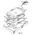
- Figure 1 is a cross sectional view of a mask focusing colour picture tube including a mask structure having two masks formed according to the present invention.
- a funnel 2 is joined to the outer periphery of a face plate 4, on the inner surface of which is formed a metal-backed phosphor screen 6.
- a neck 8 is joined to the end of funnel 2.
- Electron guns 10 are disposed within the neck 8.
- a conventional deflection apparatus 12 is mounted on the outer surfaces of funnel 2 and around neck 8.
- a first shadow mask 14 is mounted in spaced apart relation with screen 6, and a second shadow mask 16 is mounted in spaced apart relation with first shadow mask 14.
- First and second masks 14 and 16 each have a plurality of apertures extending therethrough.
- Second shadow mask 16 is mounted within face plate 4 by a mask frame 18, resilient support members 20 and pins 22.
- First shadow mask 14 is mounted on second shadow mask 16 through an insulating member 24.
- the metal-backed phosphor screen 6 has phosphor stripes of regularly alternating three colours coated on the inner surface of face plate 4, and a thin metal layer formed on the phosphor stripes.
- a conductive film 26 is uniformly coated on the inner surface of funnel 2 and on part of the inner surface of neck 8.
- Two electrical contact buttons 28 and 30 are mounted on funnel 2 for receiving electrical potentials from the outside of the CRT.
- Button 28 is electrically connected to a conductive film 26 and to a resilient conductive connector 32 connected to mask frame 18 and to the metal-backed phosphor screen layer 6 by way of pins 22.
- Button 30 is electrically connected to the first shadow mask 14 by way of a resilient conductive connector 34.
- the potential applied to metal-backed phosphor screen 6 and second mask 16 is slightly higher than the potential applied to first shadow mask 14.
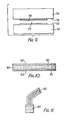
- each apertured flat mask 40, 50 includes an effective portion 41, 51 having a plurality of apertures 42, 52 therein and a non-effective portion 43, 53 surrounding the effective portion.
- Guide holes 44, 54 for positioning the masks are provided at the four corners of the non-effective portion.
- a surface plate 60 has a flat surface 61 and location pins 62. When guide holes 44, 54 of the masks are fitted over pins 62, the corresponding apertures of each mask are aligned with a high degree of precision.
- Flat mask 50 is placed on the flat surface 61 and located by the pins 62. Then first spacers 64 of insulating material are set on the non-effective portion of the flat mask and second spacers 66 extend across the effective portion. Second spacers 66 are wires which extend beyond the non-effective portion. Both first and second spacers 64 and 66 have the same thickness, which corresponds to the desired gap between the two masks of the final product. Polyamide film is preferable as the first spacer, because of ease of forming, resistance to high temperature and insulating characteristics. As the second spacer an insulated nickel chromium wire is preferred. After setting spacers 64 and 66, another flat mask 40 is stacked on the spacers and located on pins 62.
- paraffin 68 is poured on flat mask 40.
- the paraffin penetrates into the apertures of flat masks 40 and 50 and fills the remaining space between the flat masks.
- the paraffin is then cooled and becomes solidified, and so masks 40 and 50 and spacers 64 and 66 are firmly fixed together by the solidified paraffin.
- an electrical voltage is applied to the second spacers to generate heat which melts the paraffin surrounding the second spacers, which can then be pulled out from between the masks.
- the paraffin is cooled again to resolidify it.
- Figure 3 shows an enlarged cross section of the flat masks fixed by the solidified paraffin.
- Two flat masks 40 and 50 are fixed firmly by solidified paraffin 68 because of the complex configuration of apertures 42 and 52 in masks 40 and 50.
- the fixed flat masks are then simultaneously pressed to a predetermined shape, in a manner known in the prior art for pressing a shadow mask of a conventional cathode ray tube.
- the solidified paraffin filling the apertures will conform to the curvature of the mask so that sliding and non-uniform stretching of the masks is prevented.
- Figure 4 shows an enlarged cross section of the masks after pressing.
- the apertures of each flat mask are so designed as to be aligned after pressing. Even though the masks are fitted by the solidified paraffin to minimise the sliding between the masks, it is preferable to bond the first spacer to the masks with adhesive.
- the paraffin is removed from the pressed masks and then the inner mask is welded to the mask frame. Then the mask is held to the mask frame only by press forming. When the masks are thick, the other mask is held firmly. Adhesive coupling by heat resistive adhesive material to increase reliability is preferred.
- the paraffin can be removed by washing with trychroloethylene, ether or hot alcohol.
- Each flat mask has an outline of about 428 mm x 330 mm, an effective portion of about 328 mm x 290 mm and thickness of 0.30 mm.
- the gap between both masks is set at 0.5 mm respectively.
- the radius of curvature on the effective portion is about 740 mm to 800 mm.
- a wire spacer is used as the second spacer for ease of removal.
- the second spacer is not limited to the form of a wire.
- Figure 5 shows another embodiment of the invention. Plate-like spacers 69 made of, for example, cellulose acetate, are disposed over the effective portion 51 of the flat mask 50 instead of the wire spacers of the above-described embodiment.
- many spacers can be arranged on the effective portion so that the gap -between the two masks can be correctly set over the effective portion.
- Aluminium and vinyl can also be used as the second spacer even though cellulose acetate is preferred. These materials can be dissolved by a suitable solvent without any damage being caused to the masks or the first spacer.
- FIG. 9 shows such an embodiment.
- Two electromagnets 72 and 73 have flat surfaces 74 and 75 respectively facing each other. Apertured flat masks 76 and 77 are attracted to respective flat surfaces 72 and 73. Their relative positions are regulated with reference to location regulating means (not shown), for example, the guide holes through the flat masks and the location pins provided in the electromagnets.
- the first spacer 64 is placed on the non-effective portion of the flat mask 77.
- Electromagnet 72 is moved towards electromagnet 73, under the action of magnetic force, which forces the masks apart.
- paraffin is penetrated into the gap between the flat masks and into apertures from the side of the stacked masks.
- the paraffin is allowed to solidify and the electromagnets 72 and 73 are deactivated to enable the fixed flat masks to be removed.
- the masks,, fixed by the paraffin, are pressed into a predetermined shape as described above.
- paraffin 80 can be filled in the gap between non-effective portions 82 and 83 as well as the gap between effective portions 84 and 85.
- the electromagnetic apparatus shown in Figure 9 is utilised. After pressing the masks, fixing members 90 are attached at several positions on the periphery of the pressed masks as shown in Figure 11. After that, the paraffin is removed from the masks.
- paraffin is used as filling material, however, other materials can be used as paraffin substitutes as long as they meet the following criteria.
- the material must be a liquid or have a desired'viscosity so it is pourable and must be capable of being solidified in some manner after being poured.
- phenol resin, polyvinyl resin, gelatin and varnish may be used as the filling material.
- paraffin is employed because of its cheap price and its ease of handling.
- the first spacer is made of insulating material.
- conductive material for example, aluminium, can be used as the first spacer, particularly in the case where one of the masks acts as an electron shield.
Landscapes
- Engineering & Computer Science (AREA)
- Manufacturing & Machinery (AREA)
- Electrodes For Cathode-Ray Tubes (AREA)
Abstract
Description
- The present invention relates to a method of making a mask structure including two spaced apart masks for a colour cathode ray tube (CRT).
- One such CRT having this type of mask structure is the mask focusing colour picture tube. In a mask focusing colour picture tube, different potentials are applied to the masks and an electrostatic lens is formed between the adjacent masks. The electron beam utility factor is significantly increased compared with a conventional shadow mask type colour CRT. A mask focusing colour picture tube is described in Japanese Utility Model Publication No. 38930/1972, and U. S. Patents Nos. 2971117 and 3398309.
- Another type of CRT which has the above-described mask structure is described in Japanese Patent Publication No. 2698/1980. This colour CRT has two masks. One mask acts as a colour selection electrode and the other mask acts as an electron shield for preventing the first mask from being bombarded by electron beams and suffering from the effects of the bombardment.
- In both types of colour CRTs, the corresponding apertures of the masks must be aligned coaxially with the electron beams. However, it is difficult to make such a mask structure. Japanese Patent Publication No. 28188/1972 discloses a method of making such a mask structure. According to this method, on one surface of one shadow mask, a glass insulating layer is formed. Then the glass insulating layer is etched from the shadow mask side to form apertures. After that, another shadow mask is attached on the glass insulating layer. The mask structure made by this method has the glass insulating layer between two shadow masks in an effective area. Therefore, it is difficult to press-form the mask structure into a curved shape. Further, the glass insulating layer is charged up by electron beam bombardment and electron beams passing through the apertures are affected by this charge. Thus, this mask structure is not practical.
- An object of the present invention is to provide a method of making a mask structure including at least two masks for a colour CRT, which method facilitates the desired alignment for the corresponding apertures of the masks.
- Therefore, the present invention provides a method of making a mask structure for a cathode ray tube characterised in that it comprises the steps of arranging two flat masks, each mask comprising an effective portion having a plurality of apertures therethrough and a non-effective portion surrounding said effective portion, in parallel spaced apart relation with corresponding apertures aligned; filling said apertures of said flat masks and space between the masks with pourable filling material; solidifying said filling material, thereby fixing said flat masks together; simultaneously pressing said fixed flat masks into a predetermined curvature; and removing said filling material from said curved masks.
- The present invention also provides a mask structure formed by the above-described manufacturing steps.
- In order that the invention may be more readily understood, it will now be described, by way of example only, with reference to the accompanying drawings, in which:-
- Figure 1 is a cross-sectional view of a mask focusing colour cathode ray tube employing a mask structure manufactured by the method of the present invention;
- Figure 2 is a perspective view illustrating one step of the method of the present invention;
- Figure 3 is an enlarged cross section of the fixed flat masks showing one step of the invention;
- Figure 4 is an enlarged cross section of the curved masks showing one step of the invention;
- Figure 5 is a perspective view illustrating one step of the method of one embodiment of the invention;
- Figures 6 to 8 are cross sections of the curved masks showing succesive steps of the method of the invention; and
- Figures 9 to 11 are cross sections illustrating steps of the method of the invention according to alternative embodiments.
- Figure 1 is a cross sectional view of a mask focusing colour picture tube including a mask structure having two masks formed according to the present invention. A
funnel 2 is joined to the outer periphery of a face plate 4, on the inner surface of which is formed a metal-backedphosphor screen 6. A neck 8 is joined to the end offunnel 2.Electron guns 10 are disposed within the neck 8. Aconventional deflection apparatus 12 is mounted on the outer surfaces offunnel 2 and around neck 8. Afirst shadow mask 14 is mounted in spaced apart relation withscreen 6, and a second shadow mask 16 is mounted in spaced apart relation withfirst shadow mask 14. First andsecond masks 14 and 16 each have a plurality of apertures extending therethrough. Second shadow mask 16 is mounted within face plate 4 by amask frame 18,resilient support members 20 andpins 22.First shadow mask 14 is mounted on second shadow mask 16 through aninsulating member 24. - The metal-backed
phosphor screen 6 has phosphor stripes of regularly alternating three colours coated on the inner surface of face plate 4, and a thin metal layer formed on the phosphor stripes. Aconductive film 26 is uniformly coated on the inner surface offunnel 2 and on part of the inner surface of neck 8. Twoelectrical contact buttons funnel 2 for receiving electrical potentials from the outside of the CRT.Button 28 is electrically connected to aconductive film 26 and to a resilientconductive connector 32 connected tomask frame 18 and to the metal-backedphosphor screen layer 6 by way ofpins 22.Button 30 is electrically connected to thefirst shadow mask 14 by way of a resilientconductive connector 34. The potential applied to metal-backedphosphor screen 6 and second mask 16 is slightly higher than the potential applied tofirst shadow mask 14. - In the colour picture tube as described above, three
electron beams electron guns 10, and deflected bydeflection apparatus 12, are selectively focused by the second andfirst shadow masks 16 and 14, and the beams pass through their respective apertures and impinge on the appropriate phosphor stripes ofscreen 6, which then emit light of the corresponding colour. Therefore, the corresponding apertures of each mask must be arranged coaxially. The method steps according to the present invention for fabricating the masks and forming the resulting product will now be described. - Referring to Figure 2, each apertured
flat mask effective portion apertures non-effective portion Guide holes surface plate 60 has aflat surface 61 andlocation pins 62. When guideholes pins 62, the corresponding apertures of each mask are aligned with a high degree of precision. -
Flat mask 50 is placed on theflat surface 61 and located by thepins 62. Thenfirst spacers 64 of insulating material are set on the non-effective portion of the flat mask andsecond spacers 66 extend across the effective portion.Second spacers 66 are wires which extend beyond the non-effective portion. Both first andsecond spacers spacers flat mask 40 is stacked on the spacers and located onpins 62. Then heat meltedparaffin 68 is poured onflat mask 40. The paraffin penetrates into the apertures offlat masks masks spacers flat masks paraffin 68 because of the complex configuration ofapertures masks - The fixed flat masks are then simultaneously pressed to a predetermined shape, in a manner known in the prior art for pressing a shadow mask of a conventional cathode ray tube. During the pressing step, the solidified paraffin filling the apertures will conform to the curvature of the mask so that sliding and non-uniform stretching of the masks is prevented. Figure 4 shows an enlarged cross section of the masks after pressing. The apertures of each flat mask are so designed as to be aligned after pressing. Even though the masks are fitted by the solidified paraffin to minimise the sliding between the masks, it is preferable to bond the first spacer to the masks with adhesive.
- After pressing the masks, the paraffin is removed from the pressed masks and then the inner mask is welded to the mask frame. Then the mask is held to the mask frame only by press forming. When the masks are thick, the other mask is held firmly. Adhesive coupling by heat resistive adhesive material to increase reliability is preferred. The paraffin can be removed by washing with trychroloethylene, ether or hot alcohol.
- A specification of one embodiment is as follows. Each flat mask has an outline of about 428 mm x 330 mm, an effective portion of about 328 mm x 290 mm and thickness of 0.30 mm. The gap between both masks is set at 0.5 mm respectively. The radius of curvature on the effective portion is about 740 mm to 800 mm.
- In the mask structure manufactured by the above described manner, the corrresponding apertures of each mask exactly correspond to each other. No insulating spacer is left on the effective portion so that the charging drawback discussed with respect to the prior art is eliminated.
- In the above-described embodiment, a wire spacer is used as the second spacer for ease of removal. However, the second spacer is not limited to the form of a wire. Figure 5 shows another embodiment of the invention. Plate-
like spacers 69 made of, for example, cellulose acetate, are disposed over theeffective portion 51 of theflat mask 50 instead of the wire spacers of the above-described embodiment. - After setting a
first spacer 64 andsecond spacers 69, anotherflat mask 40 is placed onspacers flat mask 40. The paraffin penetrates through the apertures and fills the remaining space between the flat masks. The paraffin is then allowed to solidify. The flat masks fixed by the paraffin are then simultaneously pressed to a predetermined curvature shape as shown in Figure 6. The masks are then washed with hot alcohol and the paraffin is removed as shown in Figure 7. Then the plate-like second spacers of cellulose acetate are dissolved away by acetone as shown in Figure 8. - In this embodiment, many spacers can be arranged on the effective portion so that the gap -between the two masks can be correctly set over the effective portion. Aluminium and vinyl can also be used as the second spacer even though cellulose acetate is preferred. These materials can be dissolved by a suitable solvent without any damage being caused to the masks or the first spacer.
- Even though the above-described embodiments use the second spacers on the effective portion to keep a spacing between two masks, the second spacers can be emliminated. Figure 9 shows such an embodiment. Two
electromagnets flat surfaces flat masks flat surfaces first spacer 64 is placed on the non-effective portion of theflat mask 77.Electromagnet 72 is moved towardselectromagnet 73, under the action of magnetic force, which forces the masks apart. Under these circumstances, melted paraffin is penetrated into the gap between the flat masks and into apertures from the side of the stacked masks. The paraffin is allowed to solidify and theelectromagnets - All embodiments described above have employed first spacers between the non-effective portions of the masks. However, the first spacers also can be eliminated. As shown in Figure 10,
paraffin 80 can be filled in the gap betweennon-effective portions effective portions members 90 are attached at several positions on the periphery of the pressed masks as shown in Figure 11. After that, the paraffin is removed from the masks. - In the above-described embodiments, paraffin is used as filling material, however, other materials can be used as paraffin substitutes as long as they meet the following criteria. First, the material must be a liquid or have a desired'viscosity so it is pourable and must be capable of being solidified in some manner after being poured. Second, it must be dissolvable or decomposable in some manner. For example, phenol resin, polyvinyl resin, gelatin and varnish may be used as the filling material. In the described embodiments paraffin is employed because of its cheap price and its ease of handling.
- In the above-described embodiments, the first spacer is made of insulating material. However, conductive material, for example, aluminium, can be used as the first spacer, particularly in the case where one of the masks acts as an electron shield.
- While the invention has been described in connection with what is presently considered to be the most practical and preferred embodiments, it is to be understood that the invention is not to be limited to the disclosed embodiments but, on the contrary, is intended to cover various modifications and equivalent arrangements included with the spirit and scope of the appended claims which scope is to be accorded the broadest interpretation so as to encompass all such modifications and equivalent structures.
Claims (10)
Applications Claiming Priority (2)
| Application Number | Priority Date | Filing Date | Title |
|---|---|---|---|
| JP56193647A JPS5897243A (en) | 1981-12-03 | 1981-12-03 | Manufacture of color picture tube mask |
| JP193647/81 | 1981-12-03 |
Publications (3)
| Publication Number | Publication Date |
|---|---|
| EP0081329A2 true EP0081329A2 (en) | 1983-06-15 |
| EP0081329A3 EP0081329A3 (en) | 1984-05-16 |
| EP0081329B1 EP0081329B1 (en) | 1987-03-25 |
Family
ID=16311417
Family Applications (1)
| Application Number | Title | Priority Date | Filing Date |
|---|---|---|---|
| EP82306329A Expired EP0081329B1 (en) | 1981-12-03 | 1982-11-26 | Method of making a two mask structure for cathode ray tube |
Country Status (5)
| Country | Link |
|---|---|
| US (1) | US4540374A (en) |
| EP (1) | EP0081329B1 (en) |
| JP (1) | JPS5897243A (en) |
| KR (1) | KR860000935B1 (en) |
| DE (1) | DE3275883D1 (en) |
Cited By (3)
| Publication number | Priority date | Publication date | Assignee | Title |
|---|---|---|---|---|
| EP0157936A1 (en) * | 1984-03-28 | 1985-10-16 | Siemens Aktiengesellschaft | Moulding and coating compositions |
| WO1997006551A1 (en) * | 1995-08-04 | 1997-02-20 | Orion Electric Co., Ltd. | High-luminance-low-temperature mask for crts and fabrication of a screen using the mask |
| US5827628A (en) * | 1995-04-29 | 1998-10-27 | Orion Electric Co., Ltd. | Method of electrographically manufacturing a luminescent screen assembly for a CRT and CRT comprising a luminescent screen assembly manufacturing by the method |
Families Citing this family (3)
| Publication number | Priority date | Publication date | Assignee | Title |
|---|---|---|---|---|
| US6601949B1 (en) | 1992-08-26 | 2003-08-05 | Seiko Epson Corporation | Actuator unit for ink jet recording head |
| KR100215612B1 (en) * | 1995-02-21 | 1999-08-16 | 가네꼬 히사시 | Color cathode-ray tube |
| KR100206271B1 (en) * | 1995-08-04 | 1999-07-01 | 김영남 | Shadow mask of cathode-ray tube and method thereof |
Citations (5)
| Publication number | Priority date | Publication date | Assignee | Title |
|---|---|---|---|---|
| US2971117A (en) * | 1956-03-01 | 1961-02-07 | Rca Corp | Color-kinescopes, etc. |
| US3046202A (en) * | 1957-06-24 | 1962-07-24 | Westinghouse Electric Corp | Method of making an apertured member |
| LU53166A1 (en) * | 1966-03-10 | 1967-09-11 | ||
| US4207656A (en) * | 1976-01-16 | 1980-06-17 | U.S. Philips Corporation | Color television display tube and method of manufacturing same |
| EP0074738A2 (en) * | 1981-09-10 | 1983-03-23 | Kabushiki Kaisha Toshiba | Method for making CRT shadow masks |
Family Cites Families (5)
| Publication number | Priority date | Publication date | Assignee | Title |
|---|---|---|---|---|
| US3725065A (en) * | 1970-09-30 | 1973-04-03 | Rca Corp | Method for making a kinescope comprising a color selection mask with temporary corridors |
| NL7600420A (en) * | 1976-01-16 | 1977-07-19 | Philips Nv | ELECTRICAL DISCHARGE DEVICE. |
| US4112563A (en) * | 1977-01-13 | 1978-09-12 | U.S. Philips Corporation | Color display tube and method of manufacturing same |
| JPS57141849A (en) * | 1981-02-25 | 1982-09-02 | Toshiba Corp | Focus-mask-type color picture tube |
| JPS5844644A (en) * | 1981-09-10 | 1983-03-15 | Toshiba Corp | Manufacturing method for mask for color picture tube |
-
1981
- 1981-12-03 JP JP56193647A patent/JPS5897243A/en active Pending
-
1982
- 1982-11-26 DE DE8282306329T patent/DE3275883D1/en not_active Expired
- 1982-11-26 EP EP82306329A patent/EP0081329B1/en not_active Expired
- 1982-12-02 KR KR8205407A patent/KR860000935B1/en active
-
1985
- 1985-01-31 US US06/696,881 patent/US4540374A/en not_active Expired - Lifetime
Patent Citations (5)
| Publication number | Priority date | Publication date | Assignee | Title |
|---|---|---|---|---|
| US2971117A (en) * | 1956-03-01 | 1961-02-07 | Rca Corp | Color-kinescopes, etc. |
| US3046202A (en) * | 1957-06-24 | 1962-07-24 | Westinghouse Electric Corp | Method of making an apertured member |
| LU53166A1 (en) * | 1966-03-10 | 1967-09-11 | ||
| US4207656A (en) * | 1976-01-16 | 1980-06-17 | U.S. Philips Corporation | Color television display tube and method of manufacturing same |
| EP0074738A2 (en) * | 1981-09-10 | 1983-03-23 | Kabushiki Kaisha Toshiba | Method for making CRT shadow masks |
Cited By (4)
| Publication number | Priority date | Publication date | Assignee | Title |
|---|---|---|---|---|
| EP0157936A1 (en) * | 1984-03-28 | 1985-10-16 | Siemens Aktiengesellschaft | Moulding and coating compositions |
| US5827628A (en) * | 1995-04-29 | 1998-10-27 | Orion Electric Co., Ltd. | Method of electrographically manufacturing a luminescent screen assembly for a CRT and CRT comprising a luminescent screen assembly manufacturing by the method |
| WO1997006551A1 (en) * | 1995-08-04 | 1997-02-20 | Orion Electric Co., Ltd. | High-luminance-low-temperature mask for crts and fabrication of a screen using the mask |
| US5843601A (en) * | 1995-08-04 | 1998-12-01 | Orion Electric Co., Ltd. | High-luminance-low-temperature mask for CRTS and fabrication of a screen using the mask |
Also Published As
| Publication number | Publication date |
|---|---|
| DE3275883D1 (en) | 1987-04-30 |
| EP0081329A3 (en) | 1984-05-16 |
| EP0081329B1 (en) | 1987-03-25 |
| KR840003139A (en) | 1984-08-13 |
| KR860000935B1 (en) | 1986-07-19 |
| US4540374A (en) | 1985-09-10 |
| JPS5897243A (en) | 1983-06-09 |
Similar Documents
| Publication | Publication Date | Title |
|---|---|---|
| KR100439285B1 (en) | Coated spacer for a field emission display | |
| CA1139821A (en) | Electron multipliers with discrete dynode separating elements | |
| EP0081329B1 (en) | Method of making a two mask structure for cathode ray tube | |
| US4121131A (en) | Color television display tube and method of manufacturing same | |
| EP0548467A1 (en) | Cathode-ray tube wherein plural regions of phosphor screen are scanned independently of one another | |
| CA1071298A (en) | Post-deflection focusing method | |
| RU2157018C2 (en) | Color cathode-ray tube and method for producing mask | |
| EP0073654B1 (en) | Shadow mask arrangement and method of manufacture | |
| EP0075147B1 (en) | Method for manufacturing mask for color crt | |
| US4482334A (en) | Method for making CRT shadow masks | |
| US6476543B1 (en) | Cathode ray tube having an improved electrode assembly | |
| US5272413A (en) | Flat panel display device and a method of making the same | |
| EP0048510B1 (en) | Cathode ray tube | |
| NL7904653A (en) | COLOR IMAGE TUBE. | |
| EP1121703B1 (en) | Color picture tube having a tension focus mask | |
| EP0637051B1 (en) | Image display apparatus and method of making the same | |
| EP0108335B1 (en) | Color picture tube | |
| US4207656A (en) | Color television display tube and method of manufacturing same | |
| EP0219914A2 (en) | Method of making a colour selection deflection structure, and a colour picture display tube including a colour selection deflection structure made by the method | |
| WO2002082493A2 (en) | Method and apparatus for maintaining mask strand spatial uniformity for a crt | |
| JPS63195937A (en) | Deflection magnifying lens and cathode ray tube | |
| JPH05325821A (en) | Body structure of electron gun for cathode-ray tube | |
| JPH0352170B2 (en) | ||
| JPH0454334B2 (en) | ||
| WO2002061794A2 (en) | Color cathode lay tube and method of manufacturing the same |
Legal Events
| Date | Code | Title | Description |
|---|---|---|---|
| PUAI | Public reference made under article 153(3) epc to a published international application that has entered the european phase |
Free format text: ORIGINAL CODE: 0009012 |
|
| AK | Designated contracting states |
Designated state(s): DE FR GB |
|
| PUAL | Search report despatched |
Free format text: ORIGINAL CODE: 0009013 |
|
| AK | Designated contracting states |
Designated state(s): DE FR GB |
|
| RAP1 | Party data changed (applicant data changed or rights of an application transferred) |
Owner name: KABUSHIKI KAISHA TOSHIBA |
|
| 17P | Request for examination filed |
Effective date: 19841022 |
|
| 17Q | First examination report despatched |
Effective date: 19860619 |
|
| GRAA | (expected) grant |
Free format text: ORIGINAL CODE: 0009210 |
|
| AK | Designated contracting states |
Kind code of ref document: B1 Designated state(s): DE FR GB |
|
| ET | Fr: translation filed | ||
| REF | Corresponds to: |
Ref document number: 3275883 Country of ref document: DE Date of ref document: 19870430 |
|
| PLBE | No opposition filed within time limit |
Free format text: ORIGINAL CODE: 0009261 |
|
| STAA | Information on the status of an ep patent application or granted ep patent |
Free format text: STATUS: NO OPPOSITION FILED WITHIN TIME LIMIT |
|
| 26N | No opposition filed | ||
| REG | Reference to a national code |
Ref country code: GB Ref legal event code: 746 Effective date: 19980917 |
|
| REG | Reference to a national code |
Ref country code: FR Ref legal event code: D6 |
|
| PGFP | Annual fee paid to national office [announced via postgrant information from national office to epo] |
Ref country code: FR Payment date: 20011113 Year of fee payment: 20 |
|
| PGFP | Annual fee paid to national office [announced via postgrant information from national office to epo] |
Ref country code: GB Payment date: 20011128 Year of fee payment: 20 |
|
| PGFP | Annual fee paid to national office [announced via postgrant information from national office to epo] |
Ref country code: DE Payment date: 20011210 Year of fee payment: 20 |
|
| REG | Reference to a national code |
Ref country code: GB Ref legal event code: IF02 |
|
| PG25 | Lapsed in a contracting state [announced via postgrant information from national office to epo] |
Ref country code: GB Free format text: LAPSE BECAUSE OF EXPIRATION OF PROTECTION Effective date: 20021125 |
|
| REG | Reference to a national code |
Ref country code: GB Ref legal event code: PE20 Effective date: 20021125 |