EP0080712A2 - Sampling frequency converting apparatus - Google Patents
Sampling frequency converting apparatus Download PDFInfo
- Publication number
- EP0080712A2 EP0080712A2 EP82110938A EP82110938A EP0080712A2 EP 0080712 A2 EP0080712 A2 EP 0080712A2 EP 82110938 A EP82110938 A EP 82110938A EP 82110938 A EP82110938 A EP 82110938A EP 0080712 A2 EP0080712 A2 EP 0080712A2
- Authority
- EP
- European Patent Office
- Prior art keywords
- frequency
- read
- address
- digital signal
- memory
- Prior art date
- Legal status (The legal status is an assumption and is not a legal conclusion. Google has not performed a legal analysis and makes no representation as to the accuracy of the status listed.)
- Granted
Links
Images

Classifications
-
- H—ELECTRICITY
- H03—ELECTRONIC CIRCUITRY
- H03H—IMPEDANCE NETWORKS, e.g. RESONANT CIRCUITS; RESONATORS
- H03H17/00—Networks using digital techniques
- H03H17/02—Frequency selective networks
- H03H17/06—Non-recursive filters
- H03H17/0621—Non-recursive filters with input-sampling frequency and output-delivery frequency which differ, e.g. extrapolation; Anti-aliasing
- H03H17/0635—Non-recursive filters with input-sampling frequency and output-delivery frequency which differ, e.g. extrapolation; Anti-aliasing characterized by the ratio between the input-sampling and output-delivery frequencies
- H03H17/0685—Non-recursive filters with input-sampling frequency and output-delivery frequency which differ, e.g. extrapolation; Anti-aliasing characterized by the ratio between the input-sampling and output-delivery frequencies the ratio being rational
-
- H—ELECTRICITY
- H04—ELECTRIC COMMUNICATION TECHNIQUE
- H04B—TRANSMISSION
- H04B1/00—Details of transmission systems, not covered by a single one of groups H04B3/00 - H04B13/00; Details of transmission systems not characterised by the medium used for transmission
- H04B1/66—Details of transmission systems, not covered by a single one of groups H04B3/00 - H04B13/00; Details of transmission systems not characterised by the medium used for transmission for reducing bandwidth of signals; for improving efficiency of transmission
- H04B1/662—Details of transmission systems, not covered by a single one of groups H04B3/00 - H04B13/00; Details of transmission systems not characterised by the medium used for transmission for reducing bandwidth of signals; for improving efficiency of transmission using a time/frequency relationship, e.g. time compression or expansion
-
- H—ELECTRICITY
- H04—ELECTRIC COMMUNICATION TECHNIQUE
- H04N—PICTORIAL COMMUNICATION, e.g. TELEVISION
- H04N7/00—Television systems
- H04N7/01—Conversion of standards, e.g. involving analogue television standards or digital television standards processed at pixel level
- H04N7/0102—Conversion of standards, e.g. involving analogue television standards or digital television standards processed at pixel level involving the resampling of the incoming video signal
-
- H—ELECTRICITY
- H04—ELECTRIC COMMUNICATION TECHNIQUE
- H04N—PICTORIAL COMMUNICATION, e.g. TELEVISION
- H04N9/00—Details of colour television systems
- H04N9/64—Circuits for processing colour signals
Definitions
- This invention relates to a sampling frequency converting apparatus for a digital television signal.
- sampling frequencies are frequently used in different television systems such as NTSC, PAL and SECAM systems, or in the same television system. If a plurality of digital units adopting respective different sampling frequencies are applied in a digital television signal transmission path, a sampling frequency converting apparatus is necessary to convert a digital signal with one sampling frequency f A to a digital signal with another sampling frequency f B .
- a frequency conversion method by means of a frequency of an integer multiplication of the sampling frequencies f A and f B has already been proposed in an Article "Sampling Rate Conversion for NTSC T.V.” by B. G. Haskell, IEEE Communication Society, March 3, 1977.
- a sampling frequency converting apparatus which comprises means for temporarily storing a digital television signal, which is sampled by a first frequency, into a memory at the timing of the first frequency, means for reading out the digital television signal from the memory at the timing of a second frequency and means for interpolating the read-out digital television signal from the memory so as to produce a digital television signal which is sampled by the second frequency.
- the maximal speed for the sampling frequency conversion is determined by the greater frequency between the first and second frequencies.
- the same circuit configuration can be used for the conversion from first sampling frequency to the second sampling frequency and vice versa.
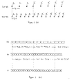
- the output data O 0 is produced from the input data I 0 and I 1 by linear interpolation.
- the output data O 1 and O 2 are produced from the output data I 0 and I 1 , and I and I 2 , respectively, by the linear interpolation.
- the same sampling points corresponding to the input data I 0 and I 1 are used for the interpolation, but their interpolation coefficients are different. This relation also holds true for the output data O 2 and 0 3 and this relation is repeated every five output data.
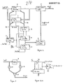
- Figure 2 shows a first embodiment of the present invention.
- the input data of the input digital television signal are applied to buffer memories 1 and 2 juxtaposed with each other and are alternately stored in the memories 1 and 2 in accordance with a write-address produced by a write-address counter 3.
- the stored data in the buffer memories I and 2 are alternately read out in accordance with a read-address produced by a read-address counter 5. Accordingly, when either one of the buffer memories 1 and 2 is in the write-mode, the other is in the read-mode.
- the write or read-mode of the memories 1 and 2 is interchanged every M input data. For example, after the M data of the input data are stored in the memory 1, the next input M data are stored in the memory 2.
- the write-address is produced in the write-in address counter by counting a clocks of the frequency f A (period T A ) and being cleared every M counts under the control of a clear pulse.
- a master counter 6 counts the second sampling pulses S B (period T ) and is cleared by the clear pulse.
- the output of the master counter 6 is applied to a memory controller 4.
- the memory controller 4 is composed of a decoder 41, a gate 42 and a flip-flop 43 as shown in Figure 2(a).
- the decoder 41 produces N timing pulses during N periods of the second sampling pulses S B .
- the last timing pulse delivered from the decoder 41 is supplied to the flip-flop 43 as the clear pulse.
- the Q and Q output of the flip-flop 43 are supplied to the memories 1 and 2 as a write/read control signal, respectively.
- the gate 42 inhibits two clocks of the second sampling pulses S B during N periods, i.e., the one clear pulse period.
- the read-address counter 5 counts the clocks delivered from the gate 42 and is cleared by the clear pulse.
- the read-address from the counter 5 is applied to the memories 1 and 3. It is noticed that the one period of the clear pulse just contains M clocks of the frequency f A and N clocks of the frequency f B .
- the sampling period in the read data alternately derived from the memories 1 and 2 is converted from T A to T B and the read data are then supplied to an interpolation filter 7, where the data at sampling points are processed for the interpolation.
- the interpolation coefficient of the interpolation filter 7 is controlled by an interpolation controller 8 in synchronism with the clocks of the frequency f B .
- the interpolation controller 8 receives the output of the master counter 6.
- Figure l(b) is a diagram showing the relationship between the write-address and the read-address supplied to the buffer memories 1 and 2, and the coefficients of the interpolation filter.
- the write-address WA repeats 0, I, 2, .... and the first three data are written to the buffer memory 1 and the next three data, to the buffer memory 2.
- the read-address RA has five addresses corresponding to the three write-addresses and the designated addresses are 0, 0, 1, 1 and 2. The flow of the read-address is performed by the gate 42 in the memory controller 4.
- a transversal filter is generally used as the interpolation filter. If coefficients to be multiplied to each delay output are k 0 - k 4 , the control output K of the interpolation controller 8 ( Figure 2) is such as shown in Figure l(b). In the embodiment shown in Figure 2, the memory controller 4 and the read-address counter can be substituted to a read-only memory (ROM) which stores the flow of the read-addresses 0, 0, 1, 1 and 2.
- ROM read-only memory
- the memory controller 4 When the sampling frequency conversion is effected between two different sampling frequencies according to the present invention, the memory controller 4, the interpolation filter 7 and the coefficient for the interpolation filter are changed in accordance with the input and output sampling frequencies. These portions to be changed are constructed by a programmable ROM (P-ROM) so as to change the content of the program in accordance with the change of the sampling frequencies and if the buffer memories have sufficient capacity, the same circuit can cope with the change of the sampling frequencies.
- P-ROM programmable ROM
- sampling frequencies of the NTSC TV system will be described by way of example.
- conversion will be considered between the sampling frequency (14. 31818 MHz), i.e., the four times subcarrier frequency which has been widely used conventionally and 13.5 MHz frequency which is scheduled to be a world-wide standard sampling frequency in a digital television signal processing.
- f A 13.5 MHz
- f 14.31818 MHz
- the buffer memories 1 and 2 in this case must have capacity to store 33 data of the input digital television signals.
- the interpolation filter 7 shown in Figure 2 a higher order interpolation filter is practically used in order to satisfy the gain and phase characteristics within a necessary frequency band.
- a second embodiment also contains two buffer memories 13 and 14.
- the second embodiment is differentiated from the first embodiment shown in Figure 2 in that the alternative interchange operation of the memories 13 and 14 is performed by switchers 15, 16, 17 and 18, and a write-address and a read-address are produced by the combination of registers 19 and 21 and adders 20 and 22.
- the address production will be described in detail hereinafter.
- the sampling frequency 13.5 MHz is converted to the sampling frequency 14.31818, for example.
- a master counter 23 counts clocks of the frequency 14.31818 and supplies the output to a decoder 24 and an interpolation controller 25.
- the decoder 24 produces a clear pulse, which is similar to the clear pulse derived from the memory controller 4 shown in Figure 2, for the registers 19 and 21 and the master counter 23.
- the write-address is produced by the combination of the register 19 and the adder 20. This combination increases the output of the register 19 by "1" in synchronism with the clocks A (13.5 MHz) and the output is supplied to the memory 13 or 14 as the write-address.
- the combination including the register 21 and the adder 22 increases the output of the register 21 by in synchronism with the clocks B (14.41818 MHz).
- the integer portion of the output of the register 21 is applied to the memory 13 or 14 as the read-address.
- the read data from the memory 13 or 14 are supplied to a transversal filter 26 where the read data are processed for the interpolation.
- sampling frequency conversion for the NTSC TV system by way of the example, sampling conversion for the PAL system or other systems can be similarly made according to the present invention.
- the present invention provides the sampling frequency converting apparatus which does not need calculation elements having high speed and yet, is extremely simple in construction.
Landscapes
- Engineering & Computer Science (AREA)
- Signal Processing (AREA)
- Multimedia (AREA)
- Computer Networks & Wireless Communication (AREA)
- Physics & Mathematics (AREA)
- Computer Hardware Design (AREA)
- Mathematical Physics (AREA)
- Television Systems (AREA)
- Transmission Systems Not Characterized By The Medium Used For Transmission (AREA)
Abstract
Description
- This invention relates to a sampling frequency converting apparatus for a digital television signal.
- When a television signal is converted into a digital television signal, different sampling frequencies are frequently used in different television systems such as NTSC, PAL and SECAM systems, or in the same television system. If a plurality of digital units adopting respective different sampling frequencies are applied in a digital television signal transmission path, a sampling frequency converting apparatus is necessary to convert a digital signal with one sampling frequency fA to a digital signal with another sampling frequency fB. To perform such the sampling frequency conversion in a purely digital manner, a frequency conversion method by means of a frequency of an integer multiplication of the sampling frequencies fA and fB has already been proposed in an Article "Sampling Rate Conversion for NTSC T.V." by B. G. Haskell, IEEE Communication Society, March 3, 1977. However, this prior art method requires a high speed logic circuit in comparison with the original sampling frequencies and must prepare different circuit constructions for the conversion (fA→fB) and the conversion (fB →fA). Hence, this methods is not advantageous in conjunction with the circuit construction, the power consumption and the cost of production.
- It is therefore an object of the present invention to provide a sampling frequency converting apparatus which does not require a high calculation speed for the conversion but makes it possible to convert one sampling frequency to the other between two sampling frequencies.
- In accordance with the present invention, there is provided a sampling frequency converting apparatus which comprises means for temporarily storing a digital television signal, which is sampled by a first frequency, into a memory at the timing of the first frequency, means for reading out the digital television signal from the memory at the timing of a second frequency and means for interpolating the read-out digital television signal from the memory so as to produce a digital television signal which is sampled by the second frequency. In the present invention, the maximal speed for the sampling frequency conversion is determined by the greater frequency between the first and second frequencies. Furthermore, the same circuit configuration can be used for the conversion from first sampling frequency to the second sampling frequency and vice versa. Hence, the advantage of the present invention is extremely greater than those of the prior art.
-
- Figure l(a) is a diagram useful for explaning the priciple of the the present invention;
- Figure l(b) is a diagram showing the operation of the embodiment of the present invention;
- Figure 2 shows one embodiment of the present invention;
- Figure 2(a) shows the block diagram of a memory controller shown in Figure 2;
- Figure 3 shows the basic construction of the interpolation filter;
- Figure 4 shows a table of an example of the coefficients of the interpolation filter shown in Figure 4; and
- Figure 5 shows another embodiment of the present invention.
- In a following description, it is initially assumpted that an input digital television signal which is sampled by a sampling frequency fA (cycle period TA) is converted to an output digital television signal which is sampled by a sampling frequency fB (cycle period TB) and that the relationship between the sampling frequency fA and the sampling frequency fB is defined by fA : fB = M : N (TA: TB = M: N) (N , M: integar).
- As clearly understood from Fig. l(a), the sample point at the M-th data in the input digital television signal is coincident with the sample point at the N-th data in the output digital television signal. Hereinafter, the case of M=3 and N=5, i.e., fA:fB= 3:5 will be described for one example. In Figure l(a), the input data, train is sequentially expressed as I0, I1, I2, I'0, I'1, I'2, ... and the converted output data train is sequentially expressed as O0, O1' O2, O3, O4, O'0, O'1, O'2, O'3, O"0, ...., respectively. The output data O0 is produced from the input data I0 and I1 by linear interpolation. Similarly, the output data O1 and O2 are produced from the output data I0 and I1, and I and I2, respectively, by the linear interpolation. Here, with respect to the output data O0 and the output data O1, the same sampling points corresponding to the input data I0 and I1 are used for the interpolation, but their interpolation coefficients are different. This relation also holds true for the output data O2 and 03 and this relation is repeated every five output data.
- Figure 2 shows a first embodiment of the present invention. The input data of the input digital television signal are applied to
buffer memories memories address counter 3. The stored data in the buffer memories I and 2 are alternately read out in accordance with a read-address produced by a read-address counter 5. Accordingly, when either one of thebuffer memories memories memory 1, the next input M data are stored in thememory 2. The write-address is produced in the write-in address counter by counting a clocks of the frequency fA (period TA) and being cleared every M counts under the control of a clear pulse. - A
master counter 6 counts the second sampling pulses SB (period T ) and is cleared by the clear pulse. The output of themaster counter 6 is applied to amemory controller 4. Thememory controller 4 is composed of a decoder 41, agate 42 and a flip-flop 43 as shown in Figure 2(a). The decoder 41 produces N timing pulses during N periods of the second sampling pulses SB. The last timing pulse delivered from the decoder 41 is supplied to the flip-flop 43 as the clear pulse. The Q and Q output of the flip-flop 43 are supplied to thememories gate 42 inhibits two clocks of the second sampling pulses SB during N periods, i.e., the one clear pulse period. - The read-
address counter 5 counts the clocks delivered from thegate 42 and is cleared by the clear pulse. The read-address from thecounter 5 is applied to thememories memories interpolation filter 7, where the data at sampling points are processed for the interpolation. The interpolation coefficient of theinterpolation filter 7 is controlled by aninterpolation controller 8 in synchronism with the clocks of the frequency fB. Theinterpolation controller 8 receives the output of themaster counter 6. - Figure l(b) is a diagram showing the relationship between the write-address and the read-address supplied to the
buffer memories buffer memory 1 and the next three data, to thebuffer memory 2. In contrast, the read-address RA has five addresses corresponding to the three write-addresses and the designated addresses are 0, 0, 1, 1 and 2. The flow of the read-address is performed by thegate 42 in thememory controller 4. These memories are arranged so that when the write-operation is made to thebuffer memory 1, the read-operation can be made to thebuffer memory 2 and the write-operation and the read-operation are not made to the same memory as described above. A transversal filter is generally used as the interpolation filter. If coefficients to be multiplied to each delay output are k0 - k4, the control output K of the interpolation controller 8 (Figure 2) is such as shown in Figure l(b). In the embodiment shown in Figure 2, thememory controller 4 and the read-address counter can be substituted to a read-only memory (ROM) which stores the flow of the read-addresses - When the sampling frequency conversion is effected between two different sampling frequencies according to the present invention, the
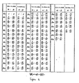
memory controller 4, theinterpolation filter 7 and the coefficient for the interpolation filter are changed in accordance with the input and output sampling frequencies. These portions to be changed are constructed by a programmable ROM (P-ROM) so as to change the content of the program in accordance with the change of the sampling frequencies and if the buffer memories have sufficient capacity, the same circuit can cope with the change of the sampling frequencies. - Next, conversion of sampling frequencies of the NTSC TV system will be described by way of example. Here, conversion will be considered between the sampling frequency (14. 31818 MHz), i.e., the four times subcarrier frequency which has been widely used conventionally and 13.5 MHz frequency which is scheduled to be a world-wide standard sampling frequency in a digital television signal processing. In this case, fA= 13.5 MHz, f = 14.31818 MHz and TA: TB = N:M = 33: 35. In Figure 2, the
buffer memories interpolation filter 7 shown in Figure 2, a higher order interpolation filter is practically used in order to satisfy the gain and phase characteristics within a necessary frequency band. For ease of explanation, linear interpolation using two adjacent sampling points such as shown in Figure 3 will be considered. The coefficients k0, k1, .... , kn, .... k34 produced from the interpolation controller becomes such as shown in Figure 4. In the sampling frequency conversion from 13.5 MHz to 14.31818 MHz, 35 pairs of coefficients a and β are used as shown in Figure 4. Since it is obvious that the alignment of the coefficients is symmetric with the center of k17 and k18, the number of the coefficients stored in the interpolation controller can be reduced by using this symmetry. On the other hand, in the sampling frequency conversion from 14. 31817 MHz to 13. 5 MHz, M:N = 35:33 , the number of the coefficients becomes 33 of k0 to k32 as also shown in Figure 4. - Referring to Fig. 5, a second embodiment also contains two
buffer memories memories switchers registers adders decoder 24 and aninterpolation controller 25. Thedecoder 24 produces a clear pulse, which is similar to the clear pulse derived from thememory controller 4 shown in Figure 2, for theregisters master counter 23. The write-address is produced by the combination of theregister 19 and theadder 20. This combination increases the output of theregister 19 by "1" in synchronism with the clocks A (13.5 MHz) and the output is supplied to thememory register 21 and theadder 22 increases the output of theregister 21 by
- The integer portion of the output of the
register 21 is applied to thememory memory transversal filter 26 where the read data are processed for the interpolation. - In the second embodiment, though the sampling frequency conversion from the lower frequency to the higher frequency is performed, it is obvious that conversion in the reverse manner can be made by changing the preset value with the same circuit construction.
- Though the foregoing illustrates the sampling frequency conversion for the NTSC TV system by way of the example, sampling conversion for the PAL system or other systems can be similarly made according to the present invention.
- As described in detail in the foregoing, the present invention provides the sampling frequency converting apparatus which does not need calculation elements having high speed and yet, is extremely simple in construction.
Claims (3)

Applications Claiming Priority (2)
| Application Number | Priority Date | Filing Date | Title |
|---|---|---|---|
| JP190312/81 | 1981-11-27 | ||
| JP56190312A JPS5892160A (en) | 1981-11-27 | 1981-11-27 | Sampling frequency converter |
Publications (3)
| Publication Number | Publication Date |
|---|---|
| EP0080712A2 true EP0080712A2 (en) | 1983-06-08 |
| EP0080712A3 EP0080712A3 (en) | 1986-11-20 |
| EP0080712B1 EP0080712B1 (en) | 1989-06-28 |
Family
ID=16256067
Family Applications (1)
| Application Number | Title | Priority Date | Filing Date |
|---|---|---|---|
| EP82110938A Expired EP0080712B1 (en) | 1981-11-27 | 1982-11-26 | Sampling frequency converting apparatus |
Country Status (4)
| Country | Link |
|---|---|
| US (1) | US4630034A (en) |
| EP (1) | EP0080712B1 (en) |
| JP (1) | JPS5892160A (en) |
| DE (1) | DE3279796D1 (en) |
Cited By (7)
| Publication number | Priority date | Publication date | Assignee | Title |
|---|---|---|---|---|
| GB2172167A (en) * | 1985-03-07 | 1986-09-10 | Sony Corp | Video signal processing |
| EP0287331A2 (en) * | 1987-04-14 | 1988-10-19 | RCA Thomson Licensing Corporation | Sampled data memory system eg for a television picture magnification system |
| EP0336669A2 (en) * | 1988-04-08 | 1989-10-11 | Sony Corporation | Sampling frequency converter |
| EP0591707A2 (en) * | 1992-10-05 | 1994-04-13 | LOEWE OPTA GmbH | Method for converting digitalized television signals |
| EP0637170A2 (en) * | 1993-07-27 | 1995-02-01 | Philips Patentverwaltung GmbH | Circuit for synchronizing a data flow |
| EP0769849A1 (en) * | 1995-10-19 | 1997-04-23 | Alcatel Espace | Method for digital wide-band filtering and filter using this method |
| GB2307128A (en) * | 1995-11-09 | 1997-05-14 | Sony Uk Ltd | Controlling video down-conversion apparatus |
Families Citing this family (15)
| Publication number | Priority date | Publication date | Assignee | Title |
|---|---|---|---|---|
| JPS60143087A (en) * | 1983-12-29 | 1985-07-29 | Nec Corp | Buffer memory control circuit |
| US5067141A (en) * | 1986-08-07 | 1991-11-19 | International Mobile Machine Corporation | Interpolator for varying a signal sampling rate |
| JPH0793548B2 (en) * | 1987-08-31 | 1995-10-09 | 三洋電機株式会社 | Sampling frequency conversion circuit |
| JP3094419B2 (en) * | 1990-02-19 | 2000-10-03 | ソニー株式会社 | Sampling rate converter |
| JPH0435111A (en) * | 1990-05-25 | 1992-02-05 | Sony Corp | Sampling rate converter |
| JP3032382B2 (en) * | 1992-07-13 | 2000-04-17 | シャープ株式会社 | Digital signal sampling frequency converter |
| US5331346A (en) * | 1992-10-07 | 1994-07-19 | Panasonic Technologies, Inc. | Approximating sample rate conversion system |
| JP2605284Y2 (en) * | 1992-12-28 | 2000-07-04 | ヤマハ株式会社 | Data converter |
| US5657261A (en) * | 1995-04-17 | 1997-08-12 | Wilson; Dennis L. | Interpolation of digital signals using signal sample replication |
| KR100218318B1 (en) | 1996-10-01 | 1999-09-01 | 문정환 | Frequency converting apparatus |
| JPH10126218A (en) * | 1996-10-15 | 1998-05-15 | Sony Corp | Sampling frequency converting device |
| EP0957579A1 (en) | 1998-05-15 | 1999-11-17 | Deutsche Thomson-Brandt Gmbh | Method and apparatus for sampling-rate conversion of audio signals |
| JP3630591B2 (en) * | 1999-08-30 | 2005-03-16 | 沖電気工業株式会社 | Clock transfer method and circuit |
| TW536827B (en) * | 2000-07-14 | 2003-06-11 | Semiconductor Energy Lab | Semiconductor display apparatus and driving method of semiconductor display apparatus |
| US7262716B2 (en) * | 2002-12-20 | 2007-08-28 | Texas Instruments Incoporated | Asynchronous sample rate converter and method |
Citations (3)
| Publication number | Priority date | Publication date | Assignee | Title |
|---|---|---|---|---|
| US3934094A (en) * | 1972-08-28 | 1976-01-20 | Hitachi, Ltd. | Frequency band converter |
| GB1455822A (en) * | 1973-05-23 | 1976-11-17 | British Broadcasting Corp | Sampling rate changer |
| GB2039195A (en) * | 1978-12-20 | 1980-07-30 | Bnritish Broadcasting Corp | Digital signal processing method and apparatus |
Family Cites Families (3)
| Publication number | Priority date | Publication date | Assignee | Title |
|---|---|---|---|---|
| US4270027A (en) * | 1979-11-28 | 1981-05-26 | International Telephone And Telegraph Corporation | Telephone subscriber line unit with sigma-delta digital to analog converter |
| US4270026A (en) * | 1979-11-28 | 1981-05-26 | International Telephone And Telegraph Corporation | Interpolator apparatus for increasing the word rate of a digital signal of the type employed in digital telephone systems |
| US4460890A (en) * | 1982-01-21 | 1984-07-17 | Sony Corporation | Direct digital to digital sampling rate conversion, method and apparatus |
-
1981
- 1981-11-27 JP JP56190312A patent/JPS5892160A/en active Granted
-
1982
- 1982-11-26 EP EP82110938A patent/EP0080712B1/en not_active Expired
- 1982-11-26 DE DE8282110938T patent/DE3279796D1/en not_active Expired
- 1982-11-29 US US06/444,915 patent/US4630034A/en not_active Expired - Lifetime
Patent Citations (3)
| Publication number | Priority date | Publication date | Assignee | Title |
|---|---|---|---|---|
| US3934094A (en) * | 1972-08-28 | 1976-01-20 | Hitachi, Ltd. | Frequency band converter |
| GB1455822A (en) * | 1973-05-23 | 1976-11-17 | British Broadcasting Corp | Sampling rate changer |
| GB2039195A (en) * | 1978-12-20 | 1980-07-30 | Bnritish Broadcasting Corp | Digital signal processing method and apparatus |
Non-Patent Citations (1)
| Title |
|---|
| PROCEEDINGS OF ICASSP 81, IEEE INTERNATIONAL CONFERENCE ON ACOUSTICS, SPEECH AND SIGNAL PROCESSING, Atlanta, Georgia, US, 30th March - 1st April 1981, vol. 1, pages 595-598, IEEE, New York, US; R. LAGADEC et al.: "A universal, digital sampling frequency converter for digital audio" * |
Cited By (16)
| Publication number | Priority date | Publication date | Assignee | Title |
|---|---|---|---|---|
| GB2172167A (en) * | 1985-03-07 | 1986-09-10 | Sony Corp | Video signal processing |
| EP0287331A2 (en) * | 1987-04-14 | 1988-10-19 | RCA Thomson Licensing Corporation | Sampled data memory system eg for a television picture magnification system |
| EP0287331A3 (en) * | 1987-04-14 | 1991-01-09 | RCA Thomson Licensing Corporation | Sampled data memory system eg for a television picture magnification system |
| EP0336669A2 (en) * | 1988-04-08 | 1989-10-11 | Sony Corporation | Sampling frequency converter |
| EP0336669A3 (en) * | 1988-04-08 | 1990-12-12 | Sony Corporation | Sampling frequency converter |
| EP0591707A2 (en) * | 1992-10-05 | 1994-04-13 | LOEWE OPTA GmbH | Method for converting digitalized television signals |
| EP0591707A3 (en) * | 1992-10-05 | 1994-06-22 | Loewe Opta Gmbh | Method for converting digitalized television signals |
| EP0637170A3 (en) * | 1993-07-27 | 1995-02-08 | Philips Patentverwaltung GmbH | Circuit for synchronizing a data flow |
| EP0637170A2 (en) * | 1993-07-27 | 1995-02-01 | Philips Patentverwaltung GmbH | Circuit for synchronizing a data flow |
| US5493589A (en) * | 1993-07-27 | 1996-02-20 | U.S. Philips Corporation | Circuit arrangement for synchronizing a data stream |
| EP0769849A1 (en) * | 1995-10-19 | 1997-04-23 | Alcatel Espace | Method for digital wide-band filtering and filter using this method |
| FR2740284A1 (en) * | 1995-10-19 | 1997-04-25 | Alcatel Espace | WIDE BAND DIGITAL FILTERING METHOD AND FILTER USING THE METHOD |
| US6125155A (en) * | 1995-10-19 | 2000-09-26 | Alcatel Espace | Broad-band digital filtering method and a filter implementing the method |
| GB2307128A (en) * | 1995-11-09 | 1997-05-14 | Sony Uk Ltd | Controlling video down-conversion apparatus |
| US5828415A (en) * | 1995-11-09 | 1998-10-27 | Sony Corporation | Apparatus for controlling video down-conversion |
| GB2307128B (en) * | 1995-11-09 | 2000-01-26 | Sony Uk Ltd | Controlling video down-conversion |
Also Published As
| Publication number | Publication date |
|---|---|
| JPS5892160A (en) | 1983-06-01 |
| JPS6357993B2 (en) | 1988-11-14 |
| EP0080712A3 (en) | 1986-11-20 |
| DE3279796D1 (en) | 1989-08-03 |
| EP0080712B1 (en) | 1989-06-28 |
| US4630034A (en) | 1986-12-16 |
Similar Documents
| Publication | Publication Date | Title |
|---|---|---|
| EP0080712A2 (en) | Sampling frequency converting apparatus | |
| CA1236914A (en) | Interlaced digital video input/filter/decimator and/or expander/interpolator filter | |
| US4496974A (en) | Conversion of the scanning line count of television pictures | |
| CA1260605A (en) | Standard converting apparatus | |
| JPH06268477A (en) | Sampling frequency converter | |
| US4471381A (en) | System for converting number of scanning lines | |
| EP0469761A2 (en) | Digital shift register using random access memory | |
| US5289292A (en) | Picture element data density conversion apparatus | |
| EP0435951B1 (en) | Video signal processing and video stores | |
| US4694413A (en) | Compact-structure input-weighted multitap digital filters | |
| US4598314A (en) | Method and apparatus for converting a video signal to a corresponding signal of lower line count | |
| US4757469A (en) | Method of addressing a random access memory as a delay line, and signal processing device including such a delay line | |
| JP2513661B2 (en) | Time axis compression multiplex transmission codec | |
| JPH05233801A (en) | Digital two-dimensional filter and two-dimensional finite impulse response (fir) filter | |
| GB2126450A (en) | Time compression of sampled signals | |
| US4977452A (en) | Sampled-value code processing device | |
| JP2965624B2 (en) | Method and circuit arrangement for digitally filtering a video signal | |
| US5153845A (en) | Time base conversion circuit | |
| KR970003101B1 (en) | Digital filter | |
| JPH0611098B2 (en) | Digital Filter | |
| JPS6214226A (en) | Semiconductor memory | |
| KR970003802Y1 (en) | A vertical decimation filter | |
| EP0562851A1 (en) | Digital signal processing using parallel filters | |
| JPS62178083A (en) | Line number transforming circuit | |
| JPS5939182A (en) | Frame memory circuit |
Legal Events
| Date | Code | Title | Description |
|---|---|---|---|
| PUAI | Public reference made under article 153(3) epc to a published international application that has entered the european phase |
Free format text: ORIGINAL CODE: 0009012 |
|
| AK | Designated contracting states |
Designated state(s): DE FR GB |
|
| RAP1 | Party data changed (applicant data changed or rights of an application transferred) |
Owner name: NEC CORPORATION |
|
| PUAL | Search report despatched |
Free format text: ORIGINAL CODE: 0009013 |
|
| AK | Designated contracting states |
Kind code of ref document: A3 Designated state(s): DE FR GB |
|
| 17P | Request for examination filed |
Effective date: 19870520 |
|
| 17Q | First examination report despatched |
Effective date: 19880201 |
|
| GRAA | (expected) grant |
Free format text: ORIGINAL CODE: 0009210 |
|
| STAA | Information on the status of an ep patent application or granted ep patent |
Free format text: STATUS: THE PATENT HAS BEEN GRANTED |
|
| AK | Designated contracting states |
Kind code of ref document: B1 Designated state(s): DE FR GB |
|
| REF | Corresponds to: |
Ref document number: 3279796 Country of ref document: DE Date of ref document: 19890803 |
|
| ET | Fr: translation filed | ||
| PLBE | No opposition filed within time limit |
Free format text: ORIGINAL CODE: 0009261 |
|
| 26N | No opposition filed | ||
| PGFP | Annual fee paid to national office [announced via postgrant information from national office to epo] |
Ref country code: FR Payment date: 20011113 Year of fee payment: 20 |
|
| PGFP | Annual fee paid to national office [announced via postgrant information from national office to epo] |
Ref country code: GB Payment date: 20011128 Year of fee payment: 20 |
|
| PGFP | Annual fee paid to national office [announced via postgrant information from national office to epo] |
Ref country code: DE Payment date: 20011210 Year of fee payment: 20 |
|
| REG | Reference to a national code |
Ref country code: GB Ref legal event code: IF02 |
|
| PG25 | Lapsed in a contracting state [announced via postgrant information from national office to epo] |
Ref country code: GB Free format text: LAPSE BECAUSE OF EXPIRATION OF PROTECTION Effective date: 20021125 |
|
| REG | Reference to a national code |
Ref country code: GB Ref legal event code: PE20 Effective date: 20021125 |