EP0077736A2 - Test vector indexing method and apparatus - Google Patents
Test vector indexing method and apparatus Download PDFInfo
- Publication number
- EP0077736A2 EP0077736A2 EP82401915A EP82401915A EP0077736A2 EP 0077736 A2 EP0077736 A2 EP 0077736A2 EP 82401915 A EP82401915 A EP 82401915A EP 82401915 A EP82401915 A EP 82401915A EP 0077736 A2 EP0077736 A2 EP 0077736A2
- Authority
- EP
- European Patent Office
- Prior art keywords
- test
- memory
- vector
- response
- address
- Prior art date
- Legal status (The legal status is an assumption and is not a legal conclusion. Google has not performed a legal analysis and makes no representation as to the accuracy of the status listed.)
- Granted
Links
- 238000012360 testing method Methods 0.000 title claims abstract description 106
- 239000013598 vector Substances 0.000 title claims abstract description 91
- 238000000034 method Methods 0.000 title claims description 10
- 230000015654 memory Effects 0.000 claims abstract description 54
- 230000004044 response Effects 0.000 claims description 49
- 238000010586 diagram Methods 0.000 description 8
- 238000005259 measurement Methods 0.000 description 6
- 238000010998 test method Methods 0.000 description 6
- 230000006870 function Effects 0.000 description 3
- 230000001154 acute effect Effects 0.000 description 1
- 238000013459 approach Methods 0.000 description 1
- 230000001143 conditioned effect Effects 0.000 description 1
- 238000013144 data compression Methods 0.000 description 1
- 230000001419 dependent effect Effects 0.000 description 1
- 230000009977 dual effect Effects 0.000 description 1
- 230000000977 initiatory effect Effects 0.000 description 1
- 238000004377 microelectronic Methods 0.000 description 1
- 238000012544 monitoring process Methods 0.000 description 1
- 238000012163 sequencing technique Methods 0.000 description 1
- 230000029305 taxis Effects 0.000 description 1
- 238000012956 testing procedure Methods 0.000 description 1
Images


Classifications
-
- G—PHYSICS
- G01—MEASURING; TESTING
- G01R—MEASURING ELECTRIC VARIABLES; MEASURING MAGNETIC VARIABLES
- G01R31/00—Arrangements for testing electric properties; Arrangements for locating electric faults; Arrangements for electrical testing characterised by what is being tested not provided for elsewhere
- G01R31/28—Testing of electronic circuits, e.g. by signal tracer
- G01R31/317—Testing of digital circuits
- G01R31/3181—Functional testing
- G01R31/3183—Generation of test inputs, e.g. test vectors, patterns or sequences
- G01R31/318371—Methodologies therefor, e.g. algorithms, procedures
-
- G—PHYSICS
- G01—MEASURING; TESTING
- G01R—MEASURING ELECTRIC VARIABLES; MEASURING MAGNETIC VARIABLES
- G01R15/00—Details of measuring arrangements of the types provided for in groups G01R17/00 - G01R29/00, G01R33/00 - G01R33/26 or G01R35/00
- G01R15/12—Circuits for multi-testers, i.e. multimeters, e.g. for measuring voltage, current, or impedance at will
-
- G—PHYSICS
- G01—MEASURING; TESTING
- G01R—MEASURING ELECTRIC VARIABLES; MEASURING MAGNETIC VARIABLES
- G01R31/00—Arrangements for testing electric properties; Arrangements for locating electric faults; Arrangements for electrical testing characterised by what is being tested not provided for elsewhere
- G01R31/28—Testing of electronic circuits, e.g. by signal tracer
- G01R31/317—Testing of digital circuits
- G01R31/3181—Functional testing
- G01R31/319—Tester hardware, i.e. output processing circuits
- G01R31/31917—Stimuli generation or application of test patterns to the device under test [DUT]
- G01R31/31919—Storing and outputting test patterns
- G01R31/31921—Storing and outputting test patterns using compression techniques, e.g. patterns sequencer
Definitions
- the present invention relates to a system for storing and retrieving digital information, and more particularly to a system for compressing the amount of digital information that is stored in a local data channel memory for a digital tester to thereby decrease the amount of storage space required to provide for a thorough exercising of an electronic component.
- test vectors are generated in a central control computer and eventually applied to various nodes on a printed circuit board to cause an electronic component on the board, such as an integrated circuit chip, to produce response signals at other nodes.
- the response signals produced by the component under test are compared with expected responses to determine whether the component is functioning properly.
- the nature of the test vectors that are applied to the nodes as stimulus signals is such that they do not harm other.components on the circuit board but they drive the node of the circuit under test sufficiently to overcome the influence of other components that might be connected to that node.
- a typical digital tester might have over 500 individual data channels through which stimulus signals are applied to the circuit board and response signals are received.
- each data channel has its own local memory that is loaded with the test vectors generated in the central control at the initiation of a test procedure.
- the local memories can apply the test vectors to the circuit board at a much faster rate than they can be generated by the computer, as well as independently of one another, to thereby substantially decrease the time it takes to thoroughly exercise all of the electronic components on the circuit board.
- RAM random access
- This implementation allows the test vectors to be applied to the nodes on the circuit board by addressing predetermined locations within the memory, and hence allows test vectors to be reused since they are not "lost" when they are read out of the memory.
- random access memories enable subroutines and looping instructions to be utilized to recall stored test vectors, so that it is not necessary to allocate one memory location for each cycle in the test procedure, thereby providing a measure of test data compression.
- one drawback associated with prior art random access type memories is the fact that they are not capable of accessing variable data when executing a sequence in the test procedure. In other words, once the test vectors are loaded from the central control computer into the RAMs, the data is fixed and the sequence of test vectors cannot be modified in response to different types of output signals from the circuit being tested.
- test pattern vectors are loaded into the RAM and are addressed with a test pattern controller.
- the shift register is loaded with variable data that can be inserted into the test pattern, for example between subroutines or loops executed with the RAM, in a first-in, first-out manner.
- a method of generating a sequence of test vectors comprising the steps of: storing a set of test vectors; storing a list of variables to be inserted in said test vector; storing a set of test pattern instructions; generating a first address signal for accessing one of said test vectors in response to a stored test pattern instruction; generating a second address signal for accessing one of said variables; and selectively employing one of said first and second address signals to access one of said test vectors or said variables in response to a stored test pattern instruction.
- Another aspect of the invention includes apparatus for generating a sequence of test vectors, comprising: a first memory for storing a first set of test vectors and a second set of test vectors representing variables to be inserted in said first set of test vectors; a second memory for storing test pattern instructions; a test pattern controller responsive to the instructions stored in said second memory for addressing said first memory to access a test vector from said first set; a vector data controller responsive to the instructions stored in said second memory for addressing said first memory to access a test vector from said second set; and switching means for selectively applying address signals from said test pattern controller or said vector data controller to said first memory in accordance with instructions from said second memory.
- FIG. 1 An in-circuit digital tester of the type to which the present invention applies is illustrated in block diagram form in Figure 1. Operation of the tester is generally controlled by a central control circuit 10 that performs such functions as generating test vectors to be applied to the components to be tested, evaluating the responses of the components to a set of applied signals, and programming the general sequence and timing of the test signals.
- An input/output interface circuit 12 connects the central control 10 with a program control circuit 14 and a sequence control circuit 16.
- the program control and sequence control circuits 14 and 16 receive data and timing signals generated by the central control
- a switching circuit 18 that also contains control switches and drive circuits.
- the program control and sequence control circuits 14 and 16 also generate timing signals that are applied to the various switches within the switching circuit 18.
- the switching circuit 18 comprises a multiplicity of data channels, each of which includes a local memory, one or more control switches, and a dri- ver/detector pair. Information is exchanged between the switching circuit 18 and a circuit board 20 under test by means of a test pin fixture 22 that connects the data channels in the switching circuit with nodes on the circuit board.
- the test pin fixture 22 can be, for example, a bed of nails type fixture that comprises an array of spring loaded pins that contact the nodes on the board 20. Where the number of pins on the fixture 22 is greater than the number of data channels in the switching circuit 18, the data channels can be selectively connected to various ones of the pins through a suitable multiplexing unit 24.
- the local memories within the switching circuit 18 are loaded with test vectors to be applied to the various nodes on the board during a test procedure. These test vectors are generated within the central control 10 and routed to appropriate memories through the program control and sequence control circuits 14 and 16. After the memories are loaded, they are selectively connected to the drivers of the data channels through the control switches in the switching circuit 18, to apply stimulus signals to the nodes of the circuit board 20. The response of the components on the board to the applied stimulus signals is compared with an expected result to determine whether the components are operating properly. This comparison can be performed within the switching circuit 18 for each individual data channel, or alternatively can be carried out within the program control circuit 14 or the central control 10.
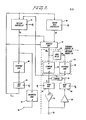
- FIG. 2 A more detailed block circuit diagram of the portions of a sequence control circuit 16 and a switching circuit 18 that implement the present invention appears in Figure 2.
- Each data channel in the switching circuit 18 includes a local memory 26 that comprises a stimulus RAM 28 and a response RAM 30.
- the stimulus RAM 28 is loaded with test vectors representing a sequence of main stimulus signals, expected response signals, and subroutines of vector signals to be applied to a node of a circuit board under test.
- the stimulus RAM 28 also contains a list of vectors representing variables to be inserted into the sequence of stimulus signals.
- the stimulus RAM 28 is connected to a driver 32 by means of a driver register 34 that receives the test vector information stored at an addressed location of the stimulus RAM 28 and applies a suitable current vector signal to the driver 32 in response to a clock pulse 0.0
- the driver 32 in turn applies an appropriate current or voltage signal to a test pin 36 that is connected to one of the nodes on the circuit board under test.
- the test pin 36 is also connected to a receiver 38 which applies any response signals received at the test pin 36 to a measurement register 40.
- the measured results in the register 40 are compared with expected results stored in the stimulus RAM 28, for example in a suitable comparator 42.
- the results of the comparison are stored in the response RAM 30.
- Address signals to be applied to the stimulus and response RAMs 28 and 30 are generated in a pattern controller 44.
- the pattern controller can be any suitable conventional device for generating address signals A in response to applied instruction signals I, such as a 2910 sequencer, for example.
- the instruction signals I that are applied to the pattern controller 44 are stored in a sequence instruction RAM 46 that receives the address signals A generated by the controller 44.
- the instruction signal that is read from the sequence RAM 46 in response to an address signal is stored in an instruction register 48 during the clock period in which the preceding instruction is applied to the pattern controller 44.
- the instruction signals I from the RAM 46 are also applied as input signals to a vector data controller 50 that produces address signals RO relating to variables that are to be inserted into the sequence of test pattern vectors being generated by the.stimulus RAM 28 in response to the address signals A from the pattern controller 44.
- the vector data controller 50 can be any suitable conventional type of indexable register, such as a 2901A register, for example.
- the address signals A and RO from both the pattern controller 44 and the vector data controller 50 are fed to an address multiplexer 52.
- the address multiplexer 52 selectively applies either the output signal A or RO from the pattern controller 44 or from the vector data controller 50 as an address signal MA to the stimulus and response RAMs 28 and 30.
- the pattern controller 44 In operation, upon the occurrence of a clock pulse O se the pattern controller 44 produces an address signal A in response to the sequence instruction In appearing at its input terminal. This address signal is applied to the multiplexer 52 and to the sequence RAM 46, causing the next sequence instruction I n+1 to be read into the instruction register 48 during the clock pulse. Simultaneously, the vector information V n-1 appearing as a data output from the stimulus RAM 28 in response to the previous address signal will be clocked into the driver register 34, to apply an appropriate current vector to the driver 32, which in turn injects a stimulus signal onto a node of the circuit under test through the test pin 36.
- the data channel functions to measure a response signal
- the signal appearing at the tested node of the circuit under test is received in the receiver 38 and clocked into a measurement register 40 during a measurement clock pulse 0 ⁇ m .
- the address signals appearing at the output terminal of the address multiplexer 52 are always one clock pulse ahead of the vectors being applied to the circuit it is necessary to delay the address to the response RAM 30 until the response comes back from the tested circuit and is clocked into the measurement register 40.
- a suitable address delay circuit 54 can be incorporated between the output terminal of the address multiplexer 52 and the address input terminal of the response RAM 30, to delay the address signal applied to the RAM by one clock period.
- the instruction from the sequence RAM 46 in addition to controlling the address output signal of the pattern controller 44,.indexes the register in the vector data controller 50 to a predetermined location relating to the address of a desired variable stored in the stimulus RAM 28.
- the address multiplexer 52 is responsive to the sequence instructions I to selectively pass either the address output signal A of the pattern controller 44, or the register output signal RO from the vector data controller 50, as an address signal MA to the stimulus and response to RAMs.
- variable data stored at predetermined locations in the stimulus RAM 28 can be injected into the pattern of test vectors read out of the RAM in response to address signals produced by the pattern controller 44.
- the address signals from the pattern controller 44 can be used to provide a diagnostic function for monitoring the operation of the tester.
- a diagnostice RAM 56 can store synchronization signals at predetermined address locations. These signals can be as simple as a single binary bit, for example.
- the pattern controller 44 When the pattern controller 44 generates the address of one of the synchronization signals, the RAM 56 will produce an output signal at a test point 58 that is external to the tester apparatus. The appearance of the synchronization signals at the test point 58 enables an operator to ascertain that the tester is at the proper test steps during a test sequence.
- the ability to insert variables into the test vector pattern is particularly advantageous in those test situations in which it is desirable to apply different stimulus signals in accordance with different responses received from the circuit under test. For example, if the response to an applied stimulus signal is the expected one, it may be desirable to continue with a predetermined test vector sequence, whereas if the response is not as expected, it may be preferable to apply a different set of vectors to assist in further defining the source of the incorrect response.
- the instruction signal from the sequence RAM 46 can be a conditional instruction which directs the pattern controller 44 to generate one of two different address signals in dependence upon a measured response.
- the pattern controller can receive an input signal, for example from the comparator 42, that indicates whether a measured response matches an expected response. The pattern controller can then generate the proper address instruction in accordance with this signal.
- the timing circuit includes a timing RAM 56 containing instructions relating to the rate at which the timing signals, such as ⁇ s and ⁇ m, are to be generated. These instructions can be written into the RAM 56 by the central control 10, for example.
- the instructions are fed to a suitably clocked timing register 58 which controls the generation of the timing signals accordingly.
- the timing instructions can also be fed to an address register 60 which determines the address of the next timing instruction signal to be read from the RAM 56.
Abstract
Description
- The present invention relates to a system for storing and retrieving digital information, and more particularly to a system for compressing the amount of digital information that is stored in a local data channel memory for a digital tester to thereby decrease the amount of storage space required to provide for a thorough exercising of an electronic component.
- In a digital tester such as an in-cir- cuit/functional electronic component tester of the type disclosed in U.S. Patent No. 3,870,953, test vectors are generated in a central control computer and eventually applied to various nodes on a printed circuit board to cause an electronic component on the board, such as an integrated circuit chip, to produce response signals at other nodes. The response signals produced by the component under test are compared with expected responses to determine whether the component is functioning properly. The nature of the test vectors that are applied to the nodes as stimulus signals is such that they do not harm other.components on the circuit board but they drive the node of the circuit under test sufficiently to overcome the influence of other components that might be connected to that node. In other digital testers for testing electronic components that are not connected to other circuits, e.g. individual IC's, or for functionally testing entire circuit boards through edge connectors, stimulus signals are similarly applied and responses are similarly measured, but the problems of harming other components and overcoming other signal levels are not present.
- A typical digital tester might have over 500 individual data channels through which stimulus signals are applied to the circuit board and response signals are received. In order to increase the rate at which the test vectors are applied to the circuit board, each data channel has its own local memory that is loaded with the test vectors generated in the central control at the initiation of a test procedure. The local memories can apply the test vectors to the circuit board at a much faster rate than they can be generated by the computer, as well as independently of one another, to thereby substantially decrease the time it takes to thoroughly exercise all of the electronic components on the circuit board.
- I As the state of microelectronics advances and integrated circuits evolve from small scale to large scale and very large scale devices, the length of a test pattern, i.e., the number of test vectors, required to thoroughly check a component increases substantially, and taxes the limits of the local memory for each data channel. This problem is particularly acute in testers which utilize shift registers to implement the local memory for each data channel. Once the contents of the memory has been shifted out of the registers, it must be reloaded with new test vectors before the test procedure can resume. The time it takes to load information into a local memory plays a significant role in the overall rate at which a device can be tested, and. hence the need to reload during a test substantially reduces the total efficiency of the test procedure. In addition, another problem associated with the shift register type memories is the fact that once a test vector is shifted out of the memory, it cannot be reused until it has been reloaded into the memory and shifted through all of its stages.
- In an effort to overcome the problems associated with shift register type memories, other testers utilize random access (RAM) type memories to store the data channel information. This implementation allows the test vectors to be applied to the nodes on the circuit board by addressing predetermined locations within the memory, and hence allows test vectors to be reused since they are not "lost" when they are read out of the memory. In addition, random access memories enable subroutines and looping instructions to be utilized to recall stored test vectors, so that it is not necessary to allocate one memory location for each cycle in the test procedure, thereby providing a measure of test data compression. However, one drawback associated with prior art random access type memories is the fact that they are not capable of accessing variable data when executing a sequence in the test procedure. In other words, once the test vectors are loaded from the central control computer into the RAMs, the data is fixed and the sequence of test vectors cannot be modified in response to different types of output signals from the circuit being tested.
- One type of memory system that attempts to overcome this problem is disclosed in an article entitled "Compressing Test Patterns To Fit Into LSI Testers" by Trent Cave, Electronics Magazine, October 12, 1978, pages 136-140. The local memory system disclosed therein utilizes both a random access memory and a shift register to store the test vectors for the data channel. Test pattern vectors are loaded into the RAM and are addressed with a test pattern controller. The shift register is loaded with variable data that can be inserted into the test pattern, for example between subroutines or loops executed with the RAM, in a first-in, first-out manner.
- Although this dual memory approach enables variable data to be inserted into a test pattern stored within a random access memory, it still suffers from the drawbacks associated with shift register memories. Specifically, once a variable in the test vector has been shifted out of the shift register memory, it cannot be reused until it has been reloaded into the memory. The need to reload the shift register each time a new variable is to be inserted into the test pattern continues to play a significant role in the overall throughput capabilities of the tester.
- Accordingly, it is a general object of the present invention to provide a method and apparatus for compressing test vector information stored in the local memory of a digital tester.
- This and other objects are attained, in accordance with one aspect of the invention, by a method of generating a sequence of test vectors, comprising the steps of: storing a set of test vectors; storing a list of variables to be inserted in said test vector; storing a set of test pattern instructions; generating a first address signal for accessing one of said test vectors in response to a stored test pattern instruction; generating a second address signal for accessing one of said variables; and selectively employing one of said first and second address signals to access one of said test vectors or said variables in response to a stored test pattern instruction.
- Another aspect of the invention includes apparatus for generating a sequence of test vectors, comprising: a first memory for storing a first set of test vectors and a second set of test vectors representing variables to be inserted in said first set of test vectors; a second memory for storing test pattern instructions; a test pattern controller responsive to the instructions stored in said second memory for addressing said first memory to access a test vector from said first set; a vector data controller responsive to the instructions stored in said second memory for addressing said first memory to access a test vector from said second set; and switching means for selectively applying address signals from said test pattern controller or said vector data controller to said first memory in accordance with instructions from said second memory.
- A more thorough appreciation of the invention and its advantages can be obtained with reference to the following detailed description of a preferred embodiment of the invention illustrated in the accompanying drawings.
-
- Figure 1 is a block circuit diagram of the general layout of an in-circuit digital tester;
- Figure 2 is a block circuit diagram of the portions of a sequence control circuit and a switching circuit that implement the present invention;
- Figure 3 is a timing diagram illustrating the variation in the clocking signals that are applied to the various sequencing control registers under different testing conditions; and
- Figure 4 is a block circuit diagram of a timing circuit that can be used to provide variable timing control.
- The preferred embodiment of the invention is described hereinafter with particular reference to its implementation in an in-circuit digital tester. It will be appreciated by those of ordinary skill in the art, - however, that the invention has more general applicability. Specifically, it can be successfully utilized in any type of digital tester that includes a memory unit for storing test vectors that are to be applied as stimulus signals to a component, including functional and individual component testers, for example.
- An in-circuit digital tester of the type to which the present invention applies is illustrated in block diagram form in Figure 1. Operation of the tester is generally controlled by a
central control circuit 10 that performs such functions as generating test vectors to be applied to the components to be tested, evaluating the responses of the components to a set of applied signals, and programming the general sequence and timing of the test signals. An input/output interface circuit 12 connects thecentral control 10 with aprogram control circuit 14 and asequence control circuit 16. The program control andsequence control circuits - 10 and generate additional timing and address signals to route data into appropriate memory units within a
switching circuit 18 that also contains control switches and drive circuits. The program control andsequence control circuits switching circuit 18. - The
switching circuit 18 comprises a multiplicity of data channels, each of which includes a local memory, one or more control switches, and a dri- ver/detector pair. Information is exchanged between theswitching circuit 18 and acircuit board 20 under test by means of atest pin fixture 22 that connects the data channels in the switching circuit with nodes on the circuit board. Thetest pin fixture 22 can be, for example, a bed of nails type fixture that comprises an array of spring loaded pins that contact the nodes on theboard 20. Where the number of pins on thefixture 22 is greater than the number of data channels in theswitching circuit 18, the data channels can be selectively connected to various ones of the pins through asuitable multiplexing unit 24. - In operation, the local memories within the
switching circuit 18 are loaded with test vectors to be applied to the various nodes on the board during a test procedure. These test vectors are generated within thecentral control 10 and routed to appropriate memories through the program control andsequence control circuits switching circuit 18, to apply stimulus signals to the nodes of thecircuit board 20. The response of the components on the board to the applied stimulus signals is compared with an expected result to determine whether the components are operating properly. This comparison can be performed within theswitching circuit 18 for each individual data channel, or alternatively can be carried out within theprogram control circuit 14 or thecentral control 10. - A more detailed block circuit diagram of the portions of a
sequence control circuit 16 and aswitching circuit 18 that implement the present invention appears in Figure 2. Each data channel in theswitching circuit 18 includes alocal memory 26 that comprises astimulus RAM 28 and aresponse RAM 30. Thestimulus RAM 28 is loaded with test vectors representing a sequence of main stimulus signals, expected response signals, and subroutines of vector signals to be applied to a node of a circuit board under test. Thestimulus RAM 28 also contains a list of vectors representing variables to be inserted into the sequence of stimulus signals. - The
stimulus RAM 28 is connected to adriver 32 by means of adriver register 34 that receives the test vector information stored at an addressed location of thestimulus RAM 28 and applies a suitable current vector signal to thedriver 32 in response to a clock pulse 0.0 Thedriver 32 in turn applies an appropriate current or voltage signal to atest pin 36 that is connected to one of the nodes on the circuit board under test. Thetest pin 36 is also connected to areceiver 38 which applies any response signals received at thetest pin 36 to ameasurement register 40. The measured results in theregister 40 are compared with expected results stored in thestimulus RAM 28, for example in asuitable comparator 42. The results of the comparison are stored in theresponse RAM 30. - Address signals to be applied to the stimulus and
response RAMs pattern controller 44. The pattern controller can be any suitable conventional device for generating address signals A in response to applied instruction signals I, such as a 2910 sequencer, for example. The instruction signals I that are applied to thepattern controller 44 are stored in asequence instruction RAM 46 that receives the address signals A generated by thecontroller 44. The instruction signal that is read from thesequence RAM 46 in response to an address signal is stored in aninstruction register 48 during the clock period in which the preceding instruction is applied to thepattern controller 44. - The instruction signals I from the
RAM 46 are also applied as input signals to avector data controller 50 that produces address signals RO relating to variables that are to be inserted into the sequence of test pattern vectors being generated bythe.stimulus RAM 28 in response to the address signals A from thepattern controller 44. Thevector data controller 50 can be any suitable conventional type of indexable register, such as a 2901A register, for example. The address signals A and RO from both thepattern controller 44 and thevector data controller 50 are fed to anaddress multiplexer 52. In response to the sequence instruction I from thesequence RAM 46, theaddress multiplexer 52 selectively applies either the output signal A or RO from thepattern controller 44 or from thevector data controller 50 as an address signal MA to the stimulus andresponse RAMs - In operation, upon the occurrence of a clock pulse Ose the
pattern controller 44 produces an address signal A in response to the sequence instruction In appearing at its input terminal. This address signal is applied to themultiplexer 52 and to thesequence RAM 46, causing the next sequence instruction In+1 to be read into theinstruction register 48 during the clock pulse. Simultaneously, the vector information Vn-1 appearing as a data output from thestimulus RAM 28 in response to the previous address signal will be clocked into thedriver register 34, to apply an appropriate current vector to thedriver 32, which in turn injects a stimulus signal onto a node of the circuit under test through thetest pin 36. - When the data channel functions to measure a response signal, in addition to, or rather than injecting a stimulus signal, the signal appearing at the tested node of the circuit under test is received in the
receiver 38 and clocked into ameasurement register 40 during a measurement clock pulse 0̸m. Since the address signals appearing at the output terminal of theaddress multiplexer 52 are always one clock pulse ahead of the vectors being applied to the circuit it is necessary to delay the address to theresponse RAM 30 until the response comes back from the tested circuit and is clocked into themeasurement register 40. Accordingly, a suitableaddress delay circuit 54 can be incorporated between the output terminal of theaddress multiplexer 52 and the address input terminal of theresponse RAM 30, to delay the address signal applied to the RAM by one clock period. - The instruction from the
sequence RAM 46, in addition to controlling the address output signal of thepattern controller 44,.indexes the register in thevector data controller 50 to a predetermined location relating to the address of a desired variable stored in thestimulus RAM 28. Theaddress multiplexer 52 is responsive to the sequence instructions I to selectively pass either the address output signal A of thepattern controller 44, or the register output signal RO from thevector data controller 50, as an address signal MA to the stimulus and response to RAMs. Hence, in accordance with the sequence instructions stored in thesequence RM 46, variable data stored at predetermined locations in thestimulus RAM 28 can be injected into the pattern of test vectors read out of the RAM in response to address signals produced by thepattern controller 44. - In addition to addressing the
stimulus RAM 28 and thesequence RAM 46, the address signals from thepattern controller 44 can be used to provide a diagnostic function for monitoring the operation of the tester. For example, adiagnostice RAM 56 can store synchronization signals at predetermined address locations. These signals can be as simple as a single binary bit, for example. When thepattern controller 44 generates the address of one of the synchronization signals, theRAM 56 will produce an output signal at atest point 58 that is external to the tester apparatus. The appearance of the synchronization signals at thetest point 58 enables an operator to ascertain that the tester is at the proper test steps during a test sequence. - The ability to insert variables into the test vector pattern is particularly advantageous in those test situations in which it is desirable to apply different stimulus signals in accordance with different responses received from the circuit under test. For example, if the response to an applied stimulus signal is the expected one, it may be desirable to continue with a predetermined test vector sequence, whereas if the response is not as expected, it may be preferable to apply a different set of vectors to assist in further defining the source of the incorrect response. In such a case, the instruction signal from the
sequence RAM 46 can be a conditional instruction which directs thepattern controller 44 to generate one of two different address signals in dependence upon a measured response. The pattern controller can receive an input signal, for example from thecomparator 42, that indicates whether a measured response matches an expected response. The pattern controller can then generate the proper address instruction in accordance with this signal. - Generally, it is desirable to apply the stimulus signals to the circuit under test at as fast a rate as possible, without waiting for the response to one stimulus signal before applying the next stimulus signal. Such a situation is illustrated in the timing diagram of Figure 3, wherein the second pulse in the signal 0., for applying the second test vector, occurs before the first pulse in the signal øm, for measuring the response to the first vector, is terminated. However, it will be apparent that such a timing procedure cannot be utilized when the vector to be applied is conditioned upon the response to a previous vector. For example, referring to Figure 3, if
Vector 3 to be applied to the component is dependent upon the response toVector 2, the measurement of such response must be completed beforeVector 3 can be applied. Similarly, whenever a HALT instruction is issued by thesequence RAM 46, the measurement of the final applied vector must take place before the testing procedure can indeed stop, as illustrated with respect toVector 4. - Accordingly, it is preferable to have a variable timing rate for controlling the operation of the
pattern controller 44 and associated registers in the data channel. One example of a circuit for producing the variable rate is illustrated in block diagram form in Figure 4. The timing circuit includes atiming RAM 56 containing instructions relating to the rate at which the timing signals, such as Øs and øm, are to be generated. These instructions can be written into theRAM 56 by thecentral control 10, for example. - The instructions are fed to a suitably clocked
timing register 58 which controls the generation of the timing signals accordingly. The timing instructions can also be fed to anaddress register 60 which determines the address of the next timing instruction signal to be read from theRAM 56. - The principles, preferred embodiments and modes of operation of the present invention have been described in the foregoing specification. The invention which is intended to be protected herein, however, is not to be construed as limited to the particular forms disclosed, since these are to be regarded as illustrative rather than restrictive. Variations and changes may be made by those skilled in the art without departing from the spirit of the invention.
Claims (10)
Applications Claiming Priority (2)
| Application Number | Priority Date | Filing Date | Title |
|---|---|---|---|
| US06/312,839 US4493045A (en) | 1981-10-19 | 1981-10-19 | Test vector indexing method and apparatus |
| US312839 | 1981-10-19 |
Publications (3)
| Publication Number | Publication Date |
|---|---|
| EP0077736A2 true EP0077736A2 (en) | 1983-04-27 |
| EP0077736A3 EP0077736A3 (en) | 1985-11-21 |
| EP0077736B1 EP0077736B1 (en) | 1989-03-22 |
Family
ID=23213245
Family Applications (1)
| Application Number | Title | Priority Date | Filing Date |
|---|---|---|---|
| EP82401915A Expired EP0077736B1 (en) | 1981-10-19 | 1982-10-19 | Test vector indexing method and apparatus |
Country Status (7)
| Country | Link |
|---|---|
| US (1) | US4493045A (en) |
| EP (1) | EP0077736B1 (en) |
| JP (1) | JPS58108475A (en) |
| KR (1) | KR890004450B1 (en) |
| AU (1) | AU558212B2 (en) |
| CA (1) | CA1198827A (en) |
| DE (1) | DE3279572D1 (en) |
Cited By (4)
| Publication number | Priority date | Publication date | Assignee | Title |
|---|---|---|---|---|
| EP0204130A2 (en) * | 1985-06-03 | 1986-12-10 | International Business Machines Corporation | Apparatus for reducing test data storage requirements for high speed VLSI circuit testing |
| GB2184555A (en) * | 1985-12-11 | 1987-06-24 | Rohde & Schwarz | Assembling a module library for the generation of a PCB test program |
| US4733148A (en) * | 1984-12-22 | 1988-03-22 | Heidelberger Druckmaschinen Ag | Method and device for brake control for a motion-monitored and controlled drive motor for a printing machine |
| US8762141B2 (en) | 2008-02-15 | 2014-06-24 | Nokia Corporation | Reduced-complexity vector indexing and de-indexing |
Families Citing this family (27)
| Publication number | Priority date | Publication date | Assignee | Title |
|---|---|---|---|---|
| US4667300A (en) * | 1983-07-27 | 1987-05-19 | Guiltech Research Company, Inc. | Computing method and apparatus |
| FR2553540B1 (en) * | 1983-10-13 | 1986-01-03 | Centre Nat Rech Scient | RANDOM TEST DEVICE FOR LOGIC CIRCUITS, ESPECIALLY MICROPROCESSORS |
| JPH0658925B2 (en) * | 1983-10-31 | 1994-08-03 | 株式会社東芝 | Integrated circuit test equipment |
| US4639919A (en) * | 1983-12-19 | 1987-01-27 | International Business Machines Corporation | Distributed pattern generator |
| US4644486A (en) * | 1984-01-09 | 1987-02-17 | Hewlett-Packard Company | Vector network analyzer with integral processor |
| US4669051A (en) * | 1984-01-09 | 1987-05-26 | Hewlett-Packard Company | Vector network analyzer with integral processor |
| DE3513551A1 (en) * | 1985-04-16 | 1986-10-16 | Wandel & Goltermann Gmbh & Co, 7412 Eningen | DIGITAL WORD GENERATOR FOR THE AUTOMATIC GENERATION OF PERIODIC PERMANENT CHARACTERS FROM N-BIT WORDS OF ALL WORD WEIGHTS AND THEIR PERMUTATIONS |
| US5043910A (en) * | 1985-04-19 | 1991-08-27 | Graphtec Kabushikikaisha | Printed circuit board function testing system |
| US4931723A (en) * | 1985-12-18 | 1990-06-05 | Schlumberger Technologies, Inc. | Automatic test system having a "true tester-per-pin" architecture |
| CA1251575A (en) * | 1985-12-18 | 1989-03-21 | A. Keith Jeffrey | Automatic test system having a "true tester-per-pin" architecture |
| US4744084A (en) * | 1986-02-27 | 1988-05-10 | Mentor Graphics Corporation | Hardware modeling system and method for simulating portions of electrical circuits |
| FR2605112B1 (en) * | 1986-10-10 | 1989-04-07 | Thomson Csf | DEVICE AND METHOD FOR GENERATING TEST VECTORS AND TEST METHOD FOR INTEGRATED CIRCUIT |
| US4856001A (en) * | 1987-05-29 | 1989-08-08 | Zehntel, Inc. | Digital in-circuit tester having channel-memory earse-preventer |
| JPH0792496B2 (en) * | 1990-11-21 | 1995-10-09 | 株式会社東芝 | Integrated circuit test equipment |
| US5321701A (en) * | 1990-12-06 | 1994-06-14 | Teradyne, Inc. | Method and apparatus for a minimal memory in-circuit digital tester |
| US5243603A (en) * | 1991-03-26 | 1993-09-07 | Hewlett-Packard Company | Method for online modification of compressed digital test vectors |
| US5235613A (en) * | 1992-03-02 | 1993-08-10 | The Boeing Company | Frequency hopping method and apparatus |
| US5390129A (en) * | 1992-07-06 | 1995-02-14 | Motay Electronics, Inc. | Universal burn-in driver system and method therefor |
| US5436849A (en) * | 1993-02-09 | 1995-07-25 | International Business Machines Corporation | Incremental logic synthesis system for efficient revision of logic circuit designs |
| US5550760A (en) * | 1993-02-18 | 1996-08-27 | Digital Equipment Corporation | Simulation of circuits |
| US5617431A (en) * | 1994-08-02 | 1997-04-01 | Advanced Micro Devices, Inc. | Method and apparatus to reuse existing test patterns to test a single integrated circuit containing previously existing cores |
| US6073263A (en) * | 1997-10-29 | 2000-06-06 | Credence Systems Corporation | Parallel processing pattern generation system for an integrated circuit tester |
| US5825787A (en) * | 1997-11-25 | 1998-10-20 | Xilinx, Inc. | System and method for accessing a test vector memory |
| US6263303B1 (en) * | 1998-10-26 | 2001-07-17 | Sony Corporation | Simulator architecture |
| US6154865A (en) * | 1998-11-13 | 2000-11-28 | Credence Systems Corporation | Instruction processing pattern generator controlling an integrated circuit tester |
| KR20050106524A (en) * | 2003-03-14 | 2005-11-09 | 주식회사 아도반테스토 | Testing apparatus, program for testing apparatus, test pattern recording medium, and method of controlling testing apparatus |
| CN1955945A (en) * | 2005-10-25 | 2007-05-02 | 国际商业机器公司 | Method and device for automatic generating test executive routine sequence of software test process |
Family Cites Families (11)
| Publication number | Priority date | Publication date | Assignee | Title |
|---|---|---|---|---|
| US3634883A (en) * | 1969-11-12 | 1972-01-11 | Honeywell Inc | Microinstruction address modification and branch system |
| JPS5439980B2 (en) * | 1972-03-24 | 1979-11-30 | ||
| JPS5410219B2 (en) * | 1973-12-07 | 1979-05-02 | ||
| US4091446A (en) * | 1975-01-24 | 1978-05-23 | Ing. C. Olivetti & C., S.P.A. | Desk top electronic computer with a removably mounted ROM |
| US4038643A (en) * | 1975-11-04 | 1977-07-26 | Burroughs Corporation | Microprogramming control system |
| US4070565A (en) * | 1976-08-18 | 1978-01-24 | Zehntel, Inc. | Programmable tester method and apparatus |
| JPS5552967A (en) * | 1978-10-13 | 1980-04-17 | Advantest Corp | Pattern signal generator |
| US4293950A (en) * | 1978-04-03 | 1981-10-06 | Nippon Telegraph And Telephone Public Corporation | Test pattern generating apparatus |
| US4307445A (en) * | 1978-11-17 | 1981-12-22 | Motorola, Inc. | Microprogrammed control apparatus having a two-level control store for data processor |
| JPS5585265A (en) * | 1978-12-23 | 1980-06-27 | Toshiba Corp | Function test evaluation device for integrated circuit |
| US4397021A (en) * | 1981-06-15 | 1983-08-02 | Westinghouse Electric Corp. | Multi-processor automatic test system |
-
1981
- 1981-10-19 US US06/312,839 patent/US4493045A/en not_active Expired - Fee Related
-
1982
- 1982-10-18 KR KR8204688A patent/KR890004450B1/en active
- 1982-10-18 CA CA000413655A patent/CA1198827A/en not_active Expired
- 1982-10-18 AU AU89457/82A patent/AU558212B2/en not_active Ceased
- 1982-10-19 JP JP57182232A patent/JPS58108475A/en active Granted
- 1982-10-19 EP EP82401915A patent/EP0077736B1/en not_active Expired
- 1982-10-19 DE DE8282401915T patent/DE3279572D1/en not_active Expired
Non-Patent Citations (2)
| Title |
|---|
| DIGEST OF PAPERS - 1980 TEST CONFERENCE, 11th-13th November 1980, paper 3.4, pages 68-73, IEEE, New York, US; H.R. SHERMAN et al.: "Low cost pattern generator for testing digital LSI devices" * |
| ELECTRONICS, vol. 51, no. 21, 12th October 1978, pages 136-140, New York, US; T. CAVE: "Compressing test patterns to fit into LSI testers" * |
Cited By (6)
| Publication number | Priority date | Publication date | Assignee | Title |
|---|---|---|---|---|
| US4733148A (en) * | 1984-12-22 | 1988-03-22 | Heidelberger Druckmaschinen Ag | Method and device for brake control for a motion-monitored and controlled drive motor for a printing machine |
| EP0204130A2 (en) * | 1985-06-03 | 1986-12-10 | International Business Machines Corporation | Apparatus for reducing test data storage requirements for high speed VLSI circuit testing |
| EP0204130A3 (en) * | 1985-06-03 | 1988-10-05 | International Business Machines Corporation | Apparatus for reducing test data storage requirements for high speed vlsi circuit testing |
| GB2184555A (en) * | 1985-12-11 | 1987-06-24 | Rohde & Schwarz | Assembling a module library for the generation of a PCB test program |
| GB2184555B (en) * | 1985-12-11 | 1990-08-01 | Rohde & Schwarz | Procedure for assembling or extending a module library for the generation of an in-circuit test program for printed circuit boards |
| US8762141B2 (en) | 2008-02-15 | 2014-06-24 | Nokia Corporation | Reduced-complexity vector indexing and de-indexing |
Also Published As
| Publication number | Publication date |
|---|---|
| EP0077736A3 (en) | 1985-11-21 |
| AU558212B2 (en) | 1987-01-22 |
| CA1198827A (en) | 1985-12-31 |
| US4493045A (en) | 1985-01-08 |
| EP0077736B1 (en) | 1989-03-22 |
| KR840002107A (en) | 1984-06-11 |
| AU8945782A (en) | 1983-04-28 |
| JPH0416752B2 (en) | 1992-03-25 |
| KR890004450B1 (en) | 1989-11-04 |
| JPS58108475A (en) | 1983-06-28 |
| DE3279572D1 (en) | 1989-04-27 |
Similar Documents
| Publication | Publication Date | Title |
|---|---|---|
| EP0077736B1 (en) | Test vector indexing method and apparatus | |
| EP0149048B1 (en) | Method and apparatus for testing semiconductor devices | |
| EP0474275B1 (en) | Automatic test equipment system using pin slice architecture | |
| EP0077237B1 (en) | Digital tester local memory data storage system | |
| US4931723A (en) | Automatic test system having a "true tester-per-pin" architecture | |
| JP3577332B2 (en) | Electronic device testing equipment | |
| EP0042222B1 (en) | Programmable sequence generator for in-circuit digital tester | |
| US4994732A (en) | Automatic test system having a "true tester-per-pin" architecture | |
| US4404519A (en) | Testing embedded arrays in large scale integrated circuits | |
| US4402081A (en) | Semiconductor memory test pattern generating apparatus | |
| US4555663A (en) | Test pattern generating apparatus | |
| US4493079A (en) | Method and system for selectively loading test data into test data storage means of automatic digital test equipment | |
| US6181151B1 (en) | Integrated circuit tester with disk-based data streaming | |
| EP0222084A2 (en) | Hierarchical test system architecture | |
| EP0228332B1 (en) | Automatic test system having a "true tester-per-pin" architecture | |
| JPH0429990B2 (en) | ||
| US4837521A (en) | Delay line control system for automatic test equipment | |
| US4433412A (en) | Method and apparatus for testing and verifying the operability of register based state machine apparatus | |
| EP0699999B1 (en) | Memory architecture for automatic test equipment using vector module table | |
| US6321352B1 (en) | Integrated circuit tester having a disk drive per channel | |
| EP0468553A2 (en) | Instrumentation system and instrumentation devices adapted for use in such a system | |
| JPH08327703A (en) | Memory architecture for automatic testing device using vector module table | |
| JPS60132336A (en) | Logic integrated circuit tester | |
| JPH11273397A (en) | Semiconductor tester | |
| JPH0894715A (en) | Semiconductor ic testing device |
Legal Events
| Date | Code | Title | Description |
|---|---|---|---|
| PUAI | Public reference made under article 153(3) epc to a published international application that has entered the european phase |
Free format text: ORIGINAL CODE: 0009012 |
|
| AK | Designated contracting states |
Designated state(s): DE FR GB IT NL SE |
|
| PUAL | Search report despatched |
Free format text: ORIGINAL CODE: 0009013 |
|
| AK | Designated contracting states |
Designated state(s): DE FR GB IT NL SE |
|
| 17P | Request for examination filed |
Effective date: 19860510 |
|
| 17Q | First examination report despatched |
Effective date: 19880427 |
|
| GRAA | (expected) grant |
Free format text: ORIGINAL CODE: 0009210 |
|
| AK | Designated contracting states |
Kind code of ref document: B1 Designated state(s): DE FR GB IT NL SE |
|
| REF | Corresponds to: |
Ref document number: 3279572 Country of ref document: DE Date of ref document: 19890427 |
|
| ITF | It: translation for a ep patent filed |
Owner name: BARZANO' E ZANARDO MILANO S.P.A. |
|
| ET | Fr: translation filed | ||
| PLBE | No opposition filed within time limit |
Free format text: ORIGINAL CODE: 0009261 |
|
| STAA | Information on the status of an ep patent application or granted ep patent |
Free format text: STATUS: NO OPPOSITION FILED WITHIN TIME LIMIT |
|
| 26N | No opposition filed | ||
| PGFP | Annual fee paid to national office [announced via postgrant information from national office to epo] |
Ref country code: FR Payment date: 19910917 Year of fee payment: 10 |
|
| PGFP | Annual fee paid to national office [announced via postgrant information from national office to epo] |
Ref country code: SE Payment date: 19910919 Year of fee payment: 10 |
|
| ITTA | It: last paid annual fee | ||
| PGFP | Annual fee paid to national office [announced via postgrant information from national office to epo] |
Ref country code: NL Payment date: 19911031 Year of fee payment: 10 |
|
| PG25 | Lapsed in a contracting state [announced via postgrant information from national office to epo] |
Ref country code: SE Effective date: 19921020 |
|
| PG25 | Lapsed in a contracting state [announced via postgrant information from national office to epo] |
Ref country code: NL Effective date: 19930501 |
|
| NLV4 | Nl: lapsed or anulled due to non-payment of the annual fee | ||
| PG25 | Lapsed in a contracting state [announced via postgrant information from national office to epo] |
Ref country code: FR Effective date: 19930630 |
|
| REG | Reference to a national code |
Ref country code: FR Ref legal event code: ST |
|
| PGFP | Annual fee paid to national office [announced via postgrant information from national office to epo] |
Ref country code: GB Payment date: 19930922 Year of fee payment: 12 |
|
| PGFP | Annual fee paid to national office [announced via postgrant information from national office to epo] |
Ref country code: DE Payment date: 19931231 Year of fee payment: 12 |
|
| PG25 | Lapsed in a contracting state [announced via postgrant information from national office to epo] |
Ref country code: GB Effective date: 19941019 |
|
| EUG | Se: european patent has lapsed |
Ref document number: 82401915.2 Effective date: 19930510 |
|
| GBPC | Gb: european patent ceased through non-payment of renewal fee |
Effective date: 19941019 |
|
| PG25 | Lapsed in a contracting state [announced via postgrant information from national office to epo] |
Ref country code: DE Effective date: 19950701 |