EP0077112B1 - External magnetic field compensator for a crt - Google Patents
External magnetic field compensator for a crt Download PDFInfo
- Publication number
- EP0077112B1 EP0077112B1 EP82302988A EP82302988A EP0077112B1 EP 0077112 B1 EP0077112 B1 EP 0077112B1 EP 82302988 A EP82302988 A EP 82302988A EP 82302988 A EP82302988 A EP 82302988A EP 0077112 B1 EP0077112 B1 EP 0077112B1
- Authority
- EP
- European Patent Office
- Prior art keywords
- ray tube
- cathode ray
- output
- magnetic field
- coupled
- Prior art date
- Legal status (The legal status is an assumption and is not a legal conclusion. Google has not performed a legal analysis and makes no representation as to the accuracy of the status listed.)
- Expired
Links
Images
Classifications
-
- H—ELECTRICITY
- H04—ELECTRIC COMMUNICATION TECHNIQUE
- H04N—PICTORIAL COMMUNICATION, e.g. TELEVISION
- H04N9/00—Details of colour television systems
- H04N9/12—Picture reproducers
- H04N9/16—Picture reproducers using cathode ray tubes
- H04N9/29—Picture reproducers using cathode ray tubes using demagnetisation or compensation of external magnetic fields
-
- H—ELECTRICITY
- H01—ELECTRIC ELEMENTS
- H01J—ELECTRIC DISCHARGE TUBES OR DISCHARGE LAMPS
- H01J2229/00—Details of cathode ray tubes or electron beam tubes
- H01J2229/0007—Elimination of unwanted or stray electromagnetic effects
- H01J2229/003—Preventing or cancelling fields entering the enclosure
- H01J2229/0038—Active means
Definitions
- This invention relates to apparatus for compensating for an external magnetic field affecting the operation of a cathode ray tube (CRT) display. Frequently it is necessary to operate a CRT display in the presence of a five gauss axial external magnetic field. With only a degaussing network in conjunction with a shield around the CRT, a 1.5 to 2 gauss axial field may be effectively cancelled. It has been suggested that Hall effect devices and fluxgate transformers may be used in conjunction with active circuitry to cancel external magnetic fields. However, these methods are very complex and high in cost.
- German patent document DE-Al-2809725 describes apparatus for compensating for an external magnetic field affecting a cathode ray tube (CRT) display, said apparatus comprising: means for generating a compensating magnetic field about said cathode ray tube; and
- the present invention is characterised by: means for generating a reference display of a given colour in a predetermined area on the face of said cathode ray tube,
- said means for controlling operates to control the strength of said compensating magnetic field in response to said output signal.
- FIG. 1 illustrates CRT 1 in combination with a block diagram of circuitry according to the invention for cancelling external magnetic fields affecting CRT 1.
- CRT 1 is provided with a degaussing coil 2 having a damped sine wave 2a of current at approximately 350 Hz applied during a time interval of one field (16.67 milliseconds) every ten seconds.
- This prior art degaussing function fully corrects for horizontal and vertical external magnetic fields and partially corrects for axial external magnetic fields.
- alternately wound coils 3, 4 are activated by current generator 5 to create a linear axial magnetic field, such as oppositely wound coils in a Hem- holtz configuration.
- Current generator 5 eliminates interaction between degaussing coil 2 and coils 3, 4 which may give rise to incomplete degaussing of the display.
- Coils 3, 4 are connected in series and are located within the shield 7 of CRT 1 which minimally projects beyond the face 10 of CRT 1.
- An axial field is created between coils 3 and 4 which "bucks" or cancels any axial magnetic field which is not counteracted by degaussing coil 2.
- Current generator 5 is a high impedance device and applies a current to coils 3, 4 in response to maximizing circuit 6.
- the invention includes the use of sensors 8 on the face 10 of CRT 1, preferably, out of view of the operator and in the four corners of the face 10.
- a raster is generated in the areas where the sensors 8 are located and the sensors 8 respond to the light created by the raster.
- the sensors 8 monitor an optical characteristic of CRT 1 such as light intensity or color purity. Maximizing the output of the light from the raster generated under each sensor coincides with an essentially pure, or single color, field over the entire CRT face 10. In color monitors, the red raster is most sensitive to purity changes. Therefore, sensors 8 with red filters 9 are preferred for use with a generated red raster.
- sensors 8 are located in the four corners of the face 10 of CRT 1 with red filter 9 located between sensor 8 and face 10.
- Red raster generator 11 is used to input information to red raster gun input port 12. During each field, generator 11 creates a red raster at the locations of the face 10 of CRT 1 which include sensors 8 and filters 9. Maximizing circuit 6 senses the output of sensors 8 and controls generator 5 to maximize sensor output. Therefore, the red gun of CRT 1 is energized within the field of view of sensors 8 which generate output signals which are a function of the "redness" of the reference area on CRT face 10 associated with each sensor.
- red raster 13 generated within the field of view of the sensor 8 has approximately the same cross-sectional area and shape as the sensor 8 and filter 9 associated therewith. However, red raster area 13 may be larger or smaller.
- Red raster generator 11 may be a line counter 14 and a pulse generator 15.
- Counter 14 counts the horizontal lines during each field of display of CRT 1 and activates pulse generator 15 during the intervals of the lines which are within the fields of view 13 of sensors 8.
- Pulse generator 15 is configured to provide pulses to red raster gun input port 12 so that the red gun is "on" while it is within the field of view of sensors 8. For example, consider a substantially square CRT display of 525 lines with 262.5 lines per field having 240 lines of display. Assume that the sensors 8 are located in the outermost corners of the CRT display and that each sensor covers 1 % of the total area of the CRT face.
- the fields of view 13 of the sensor 8 are as follows: the first 10% and the last 10% of the first 24 lines (10%) of display and of the last 24 lines (10%) of display of each field.
- pulse generator 15 would be configured to provide an "on" pulse during the first 10% and the last 10% of lines 1-24 and lines 217-240 of each field.
- the output of sensors 8 will change as a function of the amount of red light observed. This is because the external magnetic field will deflect the electron beam emitted by the red electron gun causing color impurities.
- the outputs of the sensors 8 are maximized by maximizing circuit 6 which may include peak detectors 16 for detecting the peak excitation of each sensor 8 during each field.
- Summing circuit 17 sums these detected peaks to provide an output signal which represents the average "redness" of the display for that field. Synchronization of the circuitry is accomplished by using the vertical synchronization signal pulse VS (16.67 millisecond). Upon receipt of a VS pulse, the peak detectors 16 are zeroed. During the next 16.67 millisecond field, each peak detector is charged to an amplitude representative of the red light observed by its corresponding sensor 8. Signals representing the observed light are summed by summing means 17 and stored in first sample and hold circuit 18.
- current generator 5 is slightly altered.
- the output of converter 20 may be amplified by a current amplifier 22.
- Counter 19 is changed by one least significant bit in response to the delayed VS pulse thereby causing the current provided by converter 20 to slightly change.
- the next VS pulse resets the peak detectors 16 and the process is repeated.
- the output of summing means 17 is stored in second sample and hold circuit 21.
- Comparator 22 now compares the data in the first sample and hold circuit 18 with the data in the second sample and hold circuit 21. If the data in the second sample and hold circuit 21 is greater than the data in the first sample and hold circuit 18, the up/ down count line remains unchanged because greater data in circuit 21 implies that the change in current generator 5 increased the average "redness" of the display. If the data in circuit 21 is less than the data in circuit 18, the up/down count line is reversed by comparator 22. At this period in time, the delayed VS pulse provided to counter 19 again changes the count by one least significant bit causing the current generated by converter 20 to slightly change. This sequence is continually repeated during each field.
- a 12-bit counter and a 12-bit converter may be used as the current generator depending on the size of the sensors and the accuracy desired. In addition, not all bits of the counter need be used. For example, only 9 bits of a 12-bit counter may be used.
- FIGs 4-7 are a simplified series of illustrations exemplifying the sequence of correction according to the invention.
- fields of view 13a, 13b, 13c, 13d defined by-the solid lines do not coincide with red rasters 23a, 23b, 23c, 23d defined by the dotted lines.
- the shaded area indicates the overlap. Assume that the invention is initially activated and results in creating a magnetic field which adds to rather than compensates for the external magnetic field.
Landscapes
- Engineering & Computer Science (AREA)
- Multimedia (AREA)
- Signal Processing (AREA)
- Video Image Reproduction Devices For Color Tv Systems (AREA)
- Vessels, Lead-In Wires, Accessory Apparatuses For Cathode-Ray Tubes (AREA)
- Electrodes For Cathode-Ray Tubes (AREA)
- Testing, Inspecting, Measuring Of Stereoscopic Televisions And Televisions (AREA)
Description
- The U.S. Government has rights in this invention pursuant to Contract No. DAAK20-79-C--0284 awarded by the Department of the Army. This invention relates to apparatus for compensating for an external magnetic field affecting the operation of a cathode ray tube (CRT) display. Frequently it is necessary to operate a CRT display in the presence of a five gauss axial external magnetic field. With only a degaussing network in conjunction with a shield around the CRT, a 1.5 to 2 gauss axial field may be effectively cancelled. It has been suggested that Hall effect devices and fluxgate transformers may be used in conjunction with active circuitry to cancel external magnetic fields. However, these methods are very complex and high in cost.
- German patent document DE-Al-2809725 describes apparatus for compensating for an external magnetic field affecting a cathode ray tube (CRT) display, said apparatus comprising: means for generating a compensating magnetic field about said cathode ray tube; and
- means for controlling the strength of said compensating magnetic field.
- The present invention is characterised by: means for generating a reference display of a given colour in a predetermined area on the face of said cathode ray tube,
- means for sensing an optical characteristic of the reference display and generating an output signal representative thereof; and in that
- said means for controlling operates to control the strength of said compensating magnetic field in response to said output signal.
- An embodiment of the invention will now be described, by way of example, with reference to the accompanying drawings, in which:-
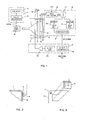
- Figure 1 is a diagram in block form illustrating an apparatus for cancelling an external magnetic field applied to a CRT in accordance with the invention.
- Figure 2 is a partial sectional view of a corner of a CRT having a photosensor and red filter mounted thereon.
- Figure 3 is a partial view of a corner of a CRT illustrating a relationship between a reference area on the CRT and a photosensor for detecting the color characteristics of the reference area.
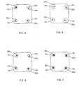
- Figures 4-7 are various views of the face of a CRT during different fields, illustrating the patterns which will occur during a compensation process according to the invention.
- In order to completely negate the effects of an external axial magnetic field on a high resolution color CRT, simple shielding methods can be employed. However, the shield must protrude past the plane of the CRT face by a distance which is a function of the amplitude of the external magnetic field. For fields of the order of 5 gauss, the shield must protrude a distance somewhat greater than three inches. This results in a tunnel effect for the operator of the CRT and is unacceptable.
- Figure 1 illustrates
CRT 1 in combination with a block diagram of circuitry according to the invention for cancelling external magneticfields affecting CRT 1. As in the prior art,CRT 1 is provided with adegaussing coil 2 having a damped sine wave 2a of current at approximately 350 Hz applied during a time interval of one field (16.67 milliseconds) every ten seconds. This prior art degaussing function fully corrects for horizontal and vertical external magnetic fields and partially corrects for axial external magnetic fields. - Operating simultaneously with
degaussing coil 2, alternately woundcoils degaussing coil 2 andcoils Coils shield 7 of CRT 1 which minimally projects beyond theface 10 of CRT 1. An axial field is created betweencoils coil 2. Current generator 5 is a high impedance device and applies a current to coils 3, 4 in response to maximizingcircuit 6. - The invention includes the use of
sensors 8 on theface 10 ofCRT 1, preferably, out of view of the operator and in the four corners of theface 10. A raster is generated in the areas where thesensors 8 are located and thesensors 8 respond to the light created by the raster. Thesensors 8 monitor an optical characteristic ofCRT 1 such as light intensity or color purity. Maximizing the output of the light from the raster generated under each sensor coincides with an essentially pure, or single color, field over theentire CRT face 10. In color monitors, the red raster is most sensitive to purity changes. Therefore,sensors 8 withred filters 9 are preferred for use with a generated red raster. - Specifically,
sensors 8 are located in the four corners of theface 10 ofCRT 1 withred filter 9 located betweensensor 8 andface 10.Red raster generator 11 is used to input information to red rastergun input port 12. During each field,generator 11 creates a red raster at the locations of theface 10 ofCRT 1 which includesensors 8 andfilters 9. Maximizingcircuit 6 senses the output ofsensors 8 and controls generator 5 to maximize sensor output. Therefore, the red gun ofCRT 1 is energized within the field of view ofsensors 8 which generate output signals which are a function of the "redness" of the reference area onCRT face 10 associated with each sensor. - As
CRT 1 is exposed to external magnetic fields, sensor outputs will change as a function of the amount of red light detected in a manner described in greater detail hereinafter. By maximizing the average "redness" observed by thesensors 8, external magnetic fields are negated. - Referring to Figure 3, the
red raster 13 generated within the field of view of thesensor 8 has approximately the same cross-sectional area and shape as thesensor 8 andfilter 9 associated therewith. However,red raster area 13 may be larger or smaller. -
Red raster generator 11 may be aline counter 14 and apulse generator 15.Counter 14 counts the horizontal lines during each field of display ofCRT 1 and activatespulse generator 15 during the intervals of the lines which are within the fields ofview 13 ofsensors 8.Pulse generator 15 is configured to provide pulses to red rastergun input port 12 so that the red gun is "on" while it is within the field of view ofsensors 8. For example, consider a substantially square CRT display of 525 lines with 262.5 lines per field having 240 lines of display. Assume that thesensors 8 are located in the outermost corners of the CRT display and that each sensor covers 1 % of the total area of the CRT face. Therefore, the fields ofview 13 of thesensor 8 are as follows: the first 10% and the last 10% of the first 24 lines (10%) of display and of the last 24 lines (10%) of display of each field. As a result,pulse generator 15 would be configured to provide an "on" pulse during the first 10% and the last 10% of lines 1-24 and lines 217-240 of each field. - As the display of
CRT 1 is exposed to external magnetic fields, the output ofsensors 8 will change as a function of the amount of red light observed. This is because the external magnetic field will deflect the electron beam emitted by the red electron gun causing color impurities. The outputs of thesensors 8 are maximized by maximizingcircuit 6 which may includepeak detectors 16 for detecting the peak excitation of eachsensor 8 during each field. Summingcircuit 17 sums these detected peaks to provide an output signal which represents the average "redness" of the display for that field. Synchronization of the circuitry is accomplished by using the vertical synchronization signal pulse VS (16.67 millisecond). Upon receipt of a VS pulse, thepeak detectors 16 are zeroed. During the next 16.67 millisecond field, each peak detector is charged to an amplitude representative of the red light observed by itscorresponding sensor 8. Signals representing the observed light are summed bysumming means 17 and stored in first sample and holdcircuit 18. - At this point in time, current generator 5 is slightly altered. Specifically, current generator 5 may be an N-
bit counter 19 responsive to a delayed VS pulse and connected to an N-bit digital-to-analog converter 20 where N = 8, 12 or any other value depending on desired sensitivity. The output ofconverter 20 may be amplified by acurrent amplifier 22.Counter 19 is changed by one least significant bit in response to the delayed VS pulse thereby causing the current provided byconverter 20 to slightly change. - The next VS pulse resets the
peak detectors 16 and the process is repeated. However, during this field the output ofsumming means 17 is stored in second sample and holdcircuit 21.Comparator 22 now compares the data in the first sample and holdcircuit 18 with the data in the second sample and holdcircuit 21. If the data in the second sample and holdcircuit 21 is greater than the data in the first sample and holdcircuit 18, the up/ down count line remains unchanged because greater data incircuit 21 implies that the change in current generator 5 increased the average "redness" of the display. If the data incircuit 21 is less than the data incircuit 18, the up/down count line is reversed bycomparator 22. At this period in time, the delayed VS pulse provided to counter 19 again changes the count by one least significant bit causing the current generated byconverter 20 to slightly change. This sequence is continually repeated during each field. - A 12-bit counter and a 12-bit converter may be used as the current generator depending on the size of the sensors and the accuracy desired. In addition, not all bits of the counter need be used. For example, only 9 bits of a 12-bit counter may be used.
- The invention, therefore, functions to maximize the average light output of the
sensors 8. In maximizing these outputs, it maximizes the red light output in the fields ofview 13 of thesensors 8. This maximizing corresponds to negation of the remaining effects of an external magnetic field which is not compensated for by degaussingcoil 2. Figures 4-7 are a simplified series of illustrations exemplifying the sequence of correction according to the invention..In Figure 4, fields ofview red rasters counter 19 resulting in initial compensation of the external magnetic field as illustrated in Figure 6. Since this initial compensation would increase the average "redness" of the display, current generator 5 would remain in the same condition and increase its current generation to further compensate for the external magnetic field as shown in Figure 7.
Claims (12)
characterised by:
Applications Claiming Priority (2)
| Application Number | Priority Date | Filing Date | Title |
|---|---|---|---|
| US06/309,947 US4380716A (en) | 1981-10-09 | 1981-10-09 | External magnetic field compensator for a CRT |
| US309947 | 1981-10-09 |
Publications (2)
| Publication Number | Publication Date |
|---|---|
| EP0077112A1 EP0077112A1 (en) | 1983-04-20 |
| EP0077112B1 true EP0077112B1 (en) | 1985-08-21 |
Family
ID=23200351
Family Applications (1)
| Application Number | Title | Priority Date | Filing Date |
|---|---|---|---|
| EP82302988A Expired EP0077112B1 (en) | 1981-10-09 | 1982-06-09 | External magnetic field compensator for a crt |
Country Status (4)
| Country | Link |
|---|---|
| US (1) | US4380716A (en) |
| EP (1) | EP0077112B1 (en) |
| JP (1) | JPS5868789A (en) |
| CA (1) | CA1165910A (en) |
Families Citing this family (21)
| Publication number | Priority date | Publication date | Assignee | Title |
|---|---|---|---|---|
| US4535270A (en) * | 1983-11-17 | 1985-08-13 | Rca Corporation | Resonant degaussing without residual magnetism |
| SE459054C (en) * | 1986-03-07 | 1992-07-30 | Philips Norden Ab | PROCEDURE FOR REDUCING MAGNETIC LEAKFIELD AND DEVICE FOR IMPLEMENTATION OF THE PROCEDURE |
| FR2629628B1 (en) * | 1988-03-29 | 1990-11-23 | Thomson Cgr | COIL, METHOD FOR PRODUCING SAID COIL, AND IMAGING DEVICE COMPRISING SUCH A COIL |
| FR2634946B1 (en) * | 1988-07-29 | 1996-04-19 | Thomson Csf | DEVICE FOR NEUTRALIZATION OF INTERFERED MAGNETIC FIELD FOR IMAGE TUBE |
| US4950955A (en) * | 1988-09-06 | 1990-08-21 | Rca Licensing Corporation | Magnetic field compensator for a CRT |
| US4963789A (en) * | 1989-05-01 | 1990-10-16 | Conrac Scd, Inc. | Method and apparatus for dynamic magnetic field neutralization |
| US5073744A (en) * | 1989-05-01 | 1991-12-17 | Interstate Electronics Corp. | Method and apparatus for dynamic magnetic field neutralization |
| US5117155A (en) * | 1989-05-01 | 1992-05-26 | Interstate Electronics Corp. | Method and apparatus employing two independent means for nulling an ambient magnetic field |
| US4996461A (en) * | 1989-09-07 | 1991-02-26 | Hughes Aircraft Company | Closed loop bucking field system |
| IT1248761B (en) * | 1990-06-08 | 1995-01-27 | Fimi Srl | COMPENSATION CIRCUIT OF THE HORIZONTAL COMPONENT OF THE TERRESTRIAL MAGNETIC FIELD FOR CINESCOPE COLOR OF HIGH RESOLUTION MONITORS |
| JP3326799B2 (en) * | 1991-05-01 | 2002-09-24 | ソニー株式会社 | Degaussing device |
| US5168195A (en) * | 1991-08-09 | 1992-12-01 | Thomson Consumer Electronics, Inc. | Magnetic field compensation apparatus |
| US5583401A (en) * | 1992-02-07 | 1996-12-10 | Matsushita Electric Industrial Co., Ltd. | Beam landing correction apparatus for a cathode ray tube |
| EP0555094A2 (en) * | 1992-02-07 | 1993-08-11 | Matsushita Electric Industrial Co., Ltd. | Beam landing correction apparatus for a cathode ray tube |
| US5465012A (en) * | 1992-12-30 | 1995-11-07 | Dunnam; Curt | Active feedback system for suppression of alternating magnetic fields |
| US5594615A (en) * | 1993-05-10 | 1997-01-14 | Mti, Inc. | Method and apparatus for reducing the intensity of magenetic field emissions from display device |
| US5561333A (en) * | 1993-05-10 | 1996-10-01 | Mti, Inc. | Method and apparatus for reducing the intensity of magnetic field emissions from video display units |
| GB2291771A (en) * | 1994-07-23 | 1996-01-31 | Ibm | Cathode ray tube display apparatus with rotatable raster |
| US5742128A (en) * | 1995-02-02 | 1998-04-21 | Orwin Associates, Inc. | Apparatus for mitigating the effects of ambient magnetic fields on the operation of a CRT |
| US5604403A (en) * | 1995-06-06 | 1997-02-18 | Aydin Corporation | Color monitor magnetic shield |
| US7456768B2 (en) * | 2006-04-07 | 2008-11-25 | Washington State University | Analog-to-digital converters based on an interleaving architecture and associated methods |
Family Cites Families (5)
| Publication number | Priority date | Publication date | Assignee | Title |
|---|---|---|---|---|
| GB1220900A (en) * | 1969-08-05 | 1971-01-27 | Mullard Ltd | Measuring the beam landing characteristic of a shadow-mask cathode-ray tube |
| US4001877A (en) * | 1975-11-26 | 1977-01-04 | Rca Corporation | Method of measuring color purity tolerance of a color display tube |
| US4035654A (en) * | 1976-01-12 | 1977-07-12 | Elmer Frank J | Optical alignment sensor |
| DE2809725C2 (en) * | 1978-03-07 | 1986-11-06 | Licentia Patent-Verwaltungs-Gmbh, 6000 Frankfurt | Image display device |
| US4240073A (en) * | 1978-05-15 | 1980-12-16 | Thomas Electronics, Inc. | Cathode ray tube display system with display location memory |
-
1981
- 1981-10-09 US US06/309,947 patent/US4380716A/en not_active Expired - Fee Related
-
1982
- 1982-06-08 CA CA000404665A patent/CA1165910A/en not_active Expired
- 1982-06-09 EP EP82302988A patent/EP0077112B1/en not_active Expired
- 1982-06-09 JP JP57099919A patent/JPS5868789A/en active Granted
Also Published As
| Publication number | Publication date |
|---|---|
| JPS5868789A (en) | 1983-04-23 |
| JPH0247752B2 (en) | 1990-10-22 |
| EP0077112A1 (en) | 1983-04-20 |
| CA1165910A (en) | 1984-04-17 |
| US4380716A (en) | 1983-04-19 |
Similar Documents
| Publication | Publication Date | Title |
|---|---|---|
| EP0077112B1 (en) | External magnetic field compensator for a crt | |
| US5066891A (en) | Magnetic field cancellation circuit | |
| US4963789A (en) | Method and apparatus for dynamic magnetic field neutralization | |
| EP0421592B1 (en) | Closed loop bucking field system | |
| US5367221A (en) | Magnetic immunity system (MIS) and monitor incorporating the MIS | |
| US4950955A (en) | Magnetic field compensator for a CRT | |
| JPH02206297A (en) | Magnetism canceling device for color cathode ray tube | |
| US5604403A (en) | Color monitor magnetic shield | |
| EP0547856B1 (en) | Field compensation for cathode ray tube monitor | |
| JPS58123288A (en) | Color television monitor | |
| CA2112307A1 (en) | Method of and apparatus for canceling electric field | |
| KR100319063B1 (en) | Cathode ray tube apparatus | |
| US5473221A (en) | Bucking field system and method for mitigating the effects of an external magnetic field on a cathode ray tube display | |
| US5488270A (en) | Color CRT display apparatus | |
| JP3216355B2 (en) | Image intensifier device | |
| KR0129959B1 (en) | Color picture tube of mis-convergence control equipment | |
| JPH03232387A (en) | Color cathode ray tube display device | |
| JPH0566726A (en) | Landing correcting device | |
| JP3804131B2 (en) | Video display device | |
| JPH06189323A (en) | Cathode-ray tube display device | |
| JPH0657051B2 (en) | External magnetic field correction device for CRT | |
| JPH0278388A (en) | Electronic display device | |
| JPH08265786A (en) | Automatically correcting device for geomagnetism | |
| JPH0673293B2 (en) | Disturbance magnetic field canceling device | |
| JPH03269283A (en) | Nuclear magnetic resonance apparatus |
Legal Events
| Date | Code | Title | Description |
|---|---|---|---|
| PUAI | Public reference made under article 153(3) epc to a published international application that has entered the european phase |
Free format text: ORIGINAL CODE: 0009012 |
|
| AK | Designated contracting states |
Designated state(s): FR GB |
|
| 17P | Request for examination filed |
Effective date: 19830914 |
|
| GRAA | (expected) grant |
Free format text: ORIGINAL CODE: 0009210 |
|
| AK | Designated contracting states |
Designated state(s): FR GB |
|
| ET | Fr: translation filed | ||
| PLBE | No opposition filed within time limit |
Free format text: ORIGINAL CODE: 0009261 |
|
| STAA | Information on the status of an ep patent application or granted ep patent |
Free format text: STATUS: NO OPPOSITION FILED WITHIN TIME LIMIT |
|
| 26N | No opposition filed | ||
| PGFP | Annual fee paid to national office [announced via postgrant information from national office to epo] |
Ref country code: FR Payment date: 19940317 Year of fee payment: 13 |
|
| PGFP | Annual fee paid to national office [announced via postgrant information from national office to epo] |
Ref country code: GB Payment date: 19940324 Year of fee payment: 13 |
|
| PG25 | Lapsed in a contracting state [announced via postgrant information from national office to epo] |
Ref country code: GB Effective date: 19950609 |
|
| GBPC | Gb: european patent ceased through non-payment of renewal fee |
Effective date: 19950609 |
|
| PG25 | Lapsed in a contracting state [announced via postgrant information from national office to epo] |
Ref country code: FR Effective date: 19960229 |
|
| REG | Reference to a national code |
Ref country code: FR Ref legal event code: ST |