EP0072857B1 - Data communication system - Google Patents
Data communication system Download PDFInfo
- Publication number
- EP0072857B1 EP0072857B1 EP82901067A EP82901067A EP0072857B1 EP 0072857 B1 EP0072857 B1 EP 0072857B1 EP 82901067 A EP82901067 A EP 82901067A EP 82901067 A EP82901067 A EP 82901067A EP 0072857 B1 EP0072857 B1 EP 0072857B1
- Authority
- EP
- European Patent Office
- Prior art keywords
- unit
- master
- register
- slave
- data
- Prior art date
- Legal status (The legal status is an assumption and is not a legal conclusion. Google has not performed a legal analysis and makes no representation as to the accuracy of the status listed.)
- Expired
Links
Images


Classifications
-
- G—PHYSICS
- G01—MEASURING; TESTING
- G01R—MEASURING ELECTRIC VARIABLES; MEASURING MAGNETIC VARIABLES
- G01R21/00—Arrangements for measuring electric power or power factor
-
- H—ELECTRICITY
- H02—GENERATION; CONVERSION OR DISTRIBUTION OF ELECTRIC POWER
- H02J—CIRCUIT ARRANGEMENTS OR SYSTEMS FOR SUPPLYING OR DISTRIBUTING ELECTRIC POWER; SYSTEMS FOR STORING ELECTRIC ENERGY
- H02J13/00—Circuit arrangements for providing remote indication of network conditions, e.g. an instantaneous record of the open or closed condition of each circuitbreaker in the network; Circuit arrangements for providing remote control of switching means in a power distribution network, e.g. switching in and out of current consumers by using a pulse code signal carried by the network
- H02J13/00006—Circuit arrangements for providing remote indication of network conditions, e.g. an instantaneous record of the open or closed condition of each circuitbreaker in the network; Circuit arrangements for providing remote control of switching means in a power distribution network, e.g. switching in and out of current consumers by using a pulse code signal carried by the network characterised by information or instructions transport means between the monitoring, controlling or managing units and monitored, controlled or operated power network element or electrical equipment
- H02J13/00007—Circuit arrangements for providing remote indication of network conditions, e.g. an instantaneous record of the open or closed condition of each circuitbreaker in the network; Circuit arrangements for providing remote control of switching means in a power distribution network, e.g. switching in and out of current consumers by using a pulse code signal carried by the network characterised by information or instructions transport means between the monitoring, controlling or managing units and monitored, controlled or operated power network element or electrical equipment using the power network as support for the transmission
- H02J13/00009—Circuit arrangements for providing remote indication of network conditions, e.g. an instantaneous record of the open or closed condition of each circuitbreaker in the network; Circuit arrangements for providing remote control of switching means in a power distribution network, e.g. switching in and out of current consumers by using a pulse code signal carried by the network characterised by information or instructions transport means between the monitoring, controlling or managing units and monitored, controlled or operated power network element or electrical equipment using the power network as support for the transmission using pulsed signals
-
- H—ELECTRICITY
- H04—ELECTRIC COMMUNICATION TECHNIQUE
- H04L—TRANSMISSION OF DIGITAL INFORMATION, e.g. TELEGRAPHIC COMMUNICATION
- H04L25/00—Baseband systems
- H04L25/38—Synchronous or start-stop systems, e.g. for Baudot code
- H04L25/40—Transmitting circuits; Receiving circuits
- H04L25/49—Transmitting circuits; Receiving circuits using code conversion at the transmitter; using predistortion; using insertion of idle bits for obtaining a desired frequency spectrum; using three or more amplitude levels ; Baseband coding techniques specific to data transmission systems
- H04L25/4902—Pulse width modulation; Pulse position modulation
-
- H—ELECTRICITY
- H04—ELECTRIC COMMUNICATION TECHNIQUE
- H04L—TRANSMISSION OF DIGITAL INFORMATION, e.g. TELEGRAPHIC COMMUNICATION
- H04L5/00—Arrangements affording multiple use of the transmission path
- H04L5/14—Two-way operation using the same type of signal, i.e. duplex
- H04L5/16—Half-duplex systems; Simplex/duplex switching; Transmission of break signals non-automatically inverting the direction of transmission
-
- Y—GENERAL TAGGING OF NEW TECHNOLOGICAL DEVELOPMENTS; GENERAL TAGGING OF CROSS-SECTIONAL TECHNOLOGIES SPANNING OVER SEVERAL SECTIONS OF THE IPC; TECHNICAL SUBJECTS COVERED BY FORMER USPC CROSS-REFERENCE ART COLLECTIONS [XRACs] AND DIGESTS
- Y02—TECHNOLOGIES OR APPLICATIONS FOR MITIGATION OR ADAPTATION AGAINST CLIMATE CHANGE
- Y02E—REDUCTION OF GREENHOUSE GAS [GHG] EMISSIONS, RELATED TO ENERGY GENERATION, TRANSMISSION OR DISTRIBUTION
- Y02E60/00—Enabling technologies; Technologies with a potential or indirect contribution to GHG emissions mitigation
-
- Y—GENERAL TAGGING OF NEW TECHNOLOGICAL DEVELOPMENTS; GENERAL TAGGING OF CROSS-SECTIONAL TECHNOLOGIES SPANNING OVER SEVERAL SECTIONS OF THE IPC; TECHNICAL SUBJECTS COVERED BY FORMER USPC CROSS-REFERENCE ART COLLECTIONS [XRACs] AND DIGESTS
- Y04—INFORMATION OR COMMUNICATION TECHNOLOGIES HAVING AN IMPACT ON OTHER TECHNOLOGY AREAS
- Y04S—SYSTEMS INTEGRATING TECHNOLOGIES RELATED TO POWER NETWORK OPERATION, COMMUNICATION OR INFORMATION TECHNOLOGIES FOR IMPROVING THE ELECTRICAL POWER GENERATION, TRANSMISSION, DISTRIBUTION, MANAGEMENT OR USAGE, i.e. SMART GRIDS
- Y04S40/00—Systems for electrical power generation, transmission, distribution or end-user application management characterised by the use of communication or information technologies, or communication or information technology specific aspects supporting them
- Y04S40/12—Systems for electrical power generation, transmission, distribution or end-user application management characterised by the use of communication or information technologies, or communication or information technology specific aspects supporting them characterised by data transport means between the monitoring, controlling or managing units and monitored, controlled or operated electrical equipment
- Y04S40/121—Systems for electrical power generation, transmission, distribution or end-user application management characterised by the use of communication or information technologies, or communication or information technology specific aspects supporting them characterised by data transport means between the monitoring, controlling or managing units and monitored, controlled or operated electrical equipment using the power network as support for the transmission
Abstract
Description
- This invention relates to a data communication system for the exchange of serial digital signal information between a programmable power meter and a remote programming/readout unit.
- It is known to provide a programmable multiple rate kilowatt hour meter for use in measuring electrical energy consumption at the premises of individual electric utility customers. Such a meter is typically completely enclosed within a weatherproof housing. The communication system of the present invention is intended to provide means for signal coupling to that meter by a separate electrical device to program the meter and to read out customer billing information. That function is carried out through the data communication system of the present invention by communication with a separate signal processing unit which can be placed in proximity and coupled with the meter. Optical coupling is preferred since this is quick and convenient without threatening the physical integrity of the meter housing.
- The rules of operation by which communications are carried out between such electrical devices over such a communication channel are important in determining the design of the data communication system.
- In FR-A-950746 there is described a duplex communication system in which pulse modulated signals are transmitted and received over a data channel at a controlled radio frequency. Master and slave processing units are connected at opposite ends of the channel, each being selectively operable to function either as a sending unit or as a receiving unit. There is, however, no provision for controlling the rate or time at which binary data is communicated, particularly when data transmission is on an irregular basis. The system is not therefore suitable for use between a programmable power meter and a remote programming/readout unit where data is transferred only in the intervals when the meter is not performing its normal metering function.
- US-A-4061975 discloses self-clocking pulse width modulators and demodulators for transmitting digital data over a single communication line.
- US-A-3,310,626 discloses an automatic telegraph transmission system in which the telegraph signals are of the type in which each character consists of a "start" unit, a plurality of data units, and a "stop" unit. The system incorporates series-to-parallel shift registers in which detection of a "start" unit in the "start" stage of the register indicates that the register is full.
- The present invention provides an improved data communication system operating in accordance with very simple rules, or modes of operation, and providing a significant improvement over prior data communication systems between programmable power meters and remote programming/readout units.
- According to the present invention there is provided a data communication system for exchanging digital signal information between a programmable power meter and a remote programming/readout unit, the system comprising master and slave processing units adapted to be communicatively coupled to opposite ends of a data channel, each of the processing units being selectively operable to function either as a sending unit or as a receiving unit, characterised in that the master processing unit includes a master control unit responsive to control signals (EMC) generated by the power meter to emit clock pulse signals, and responsive to a message received from the slave processing unit for determining the said operating function of the processing units, each of the units including a send register for storing the data to be transmitted and a receive register for receiving the transmitted data, the master unit further including gating means responsive to the clock pulse signals and to the output of the master send register such that, with the master unit operating as a sending unit, a meter reading stored as binary bits in the send register is serially transferred over the data channel to the receive register in the slave unit, and such that, with the master unit operating as a receiving unit, the clock pulse signals are transferred over the data channel to the slave unit, the slave unit further including means responsive to the clock pulse signals received from the master unit and to the output of the slave send register such that, with the slave unit operating as a sending unit, data bits representing a message signal stored in the slave send register are serially transferred over the data channel to the receive register in the master unit, the serial data transfer being such that the data bits are transmitted as long and short pulses, each data bit being transmitted at a pulse of the clock pulse signals emitted by the master control unit such that each clock pulse forms at least part of each data bit transferred in either direction over the data channel.
- In the accompanying drawings, by way of example only:
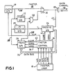
- FIG. 1 is a schematic circuit diagram of a master processing unit which is one unit of a preferred embodiment of the data communication system of this invention for transmitting and receiving data through a data channel to and from another processing unit.
- FIG. 2 is a schematic circuit diagram of a slave processing unit forming a part of the preferred embodiment of the data communication system in accordance with the present invention for transmitting and receiving data through a data channel to and from the master processing unit of FIG. 1.
- FIG. 3 is a timing diagram showing idealized wave forms of the pulse signals, and the timing relationships between pulse signals generated and received by the master and slave processing units of FIGS. 1 and 2 during the sending and receiving of information over the interconnecting data channel.
- Reference is now made to FIGS. 1 and 2 where there is shown, collectively, a data communication system comprised of a master processing unit 12 (FIG. 1) and a slave processing unit 14 (FIG. 2) communicatively coupled via a
data channel 16.Data channel 16 is shown in both FIG. 1 and FIG. 2. - The communication
link data channel 16 coupling between themaster 12 and theslave 14 can be established by various known means. For example, thedata channel 16 can be coupled optically or magnetically, or by direct electrical connection. In the preferred embodiment of the present invention, the data is to be transmitted and received between amaster 12 and aslave 14 wherein the master processing unit serves amaster user unit 18 which comprises a progra- mable multiple rate kilowatt hour meter and the slave processing unit comprises a unit for transmitting commands to that kilowatt hour meter and receiving readings from that kilowatt hour meter. In such a system, it is important to be able to very conveniently bring the portable slave processing unit into a physically coupled relationship with themaster processing unit 12 through thedata channel 16. For this purpose, an optical coupling is preferred. Since data is to be transmitted and received through the data channel by each of theprocessing units master processing unit 12, and at 15 for theslave processing unit 14. - Regardless of the type of coupling used, all information exchanged between the
master 12 andslave 14 is in serial digital signal form. That is, all information transferred over thedata channel 16 is in the form of pulses having binary states (i.e. "1" or "0"). It is a unique feature of the present invention that a logic 0 is transmitted as a short pulse, and a logic 1 is transmitted as a long pulse. The serial binary digital signals are combined in groups to convey messages, commands, or information items to be operated upon or processed. Such digital signal groups are generally referred to below as messages. - The
master 12 serves a master unit 18 (hereinafter referred to as master user 18). The master processing unit includes a master receive one-shot pulse generator 20, a master send one-shot pulse generator 22, a mastersend shift register 24, a masterreceive shift register 26, a clock one-shot pulse generator 28, an AND-gate 30, an OR-gate 32, and a master control 34. The master control 34 can be implemented with conventional discrete logic elements, or preferably by a microprocessor such as an RCA 1802. Abi-directional data bus 36interconnects master user 18, master control 34, receiveregister 26, and sendregister 36. - The
master user 18 includes an independent microprocessor. Themaster user 18 may also be implemented with an RCA 1802 microprocessor. In the preferred embodiment, themaster user 18 also comprises a programmable multiple rate kilowatt-hour meter as previously mentioned above. - The microprocessor of the programmable meter (master user 18) typically operates almost continuously to perform many important functions other than communication with
slave 14, such as measurement of power consumption, calculation of peak and demand power consumption at prescribed intervals, and switching loads on and off. - The performance and completion of these functions takes precedence over all external communications with the meter. That is, the meter (master user 18) is programmed to give precedence to the performance of its internal functions, and will communicate externally with the programmer/reader (slave 14) only when it has time to do so. The
master user 18 operates completely independently and asynchronously of the communicationmaster processing unit 12. Themaster user 18 will signal the master control 34 when themaster user 18 is available to participate in an information transfer between themaster user 12 and theslave 14. - The
slave processing unit 14 of FIG. 2 is quite similar in structure tomaster 12. The main structural difference between theslave 14 and themaster 12 is that the former does not contain a clock one-shot pulse generator 28 orgates - The
slave 14 is comprised of a slave send one-shot pulse generator 44, a slave receive one-shot pulse generator 46, a slavereceive shift register 48, a slavesend shift register 50, aslave control 52, and aslave user unit 54. Abi-directional data bus 56 is also provided to interconnect thecontrol 52,user 54 and registers 48 and 50 in a manner similar tobus 36 in themaster 12. Signal lines running between theslave user 54 and theslave control 52 carry similar nomenclature as that illustrated in FIG. 1 betweenmaster user 18 and master control 34. Further, aload line 58,clear lines 60 and 62, an enable send register (ESRG) line and an enable receive register (EERG) line are provided for controlling the send and receiveregisters master 12. - The
slave user 54 of FIG. 2 is preferably implemented by a microprocessor, such as an INTEL 8085, and contains its own program for communicating with theslave control 52. Theslave control 52 may be substantially identical to the master control 34. To cause theslave user 54 to carry out various operations, such as read or write to thedata bus 56, or to cause theslave 14 to send or receive digital signal information, a plurality ofaction control switches 64 are provided. As previously mentioned, theslave 14 in the preferred embodiment, is a microprocessor based meter programmer/reader apparatus. For that purpose, the selective activation of thevarious switches 64 will provide input control signals to theslave user 54, directing the performance of selected functions. - FIG. 3 is an idealized pulse wave form diagram indicating the relative initiation times and durations of the various pulses emitted by different components of the
master unit 12 and theslave unit 14. The first curve 68 illustrates the pulses emitted by theclock 28 each time a binary bit of information is to be transmitted by either unit and received by the other. Thecurve 70 represents the timing and duration of the pulses emitted by either the MSEND or SSEND one-shot pulse generator whenever the associated unit (12, 14) is transmitting. Similarly, curve 72 represents the relative timing and duration of the pulses emitted by either the MRECEIVE or the SRECEIVE one-shot pulse generator whenever the associated unit (12, 14) is receiving. Curve 74 illustrates the relative duration of each of the pulses transmitted through the data channel signifying a logic 1. Curve 76 illustrates the timing and the duration of each of the pulses transmitted through the data channel signifying a logic 0. - The following is a brief description of the transmission of data from master 12 (FIG. 1) to slave 14 (FIG. 2) with reference to the curves of FIG. 3. Whenever a bit (a binary digit) of information is to be transmitted, the master control 34 issues a clock pulse on a
control line 35 to the clock one-shot pulse generator 28. In response to that signal, theclock pulse generator 28 generates a short clock pulse onoutput connection 25. The leading edge of that pulse is indicated at 78 in the curve 68 of FIG. 3. Prior to the commencement of the issuance of clock pulses by theclock 28, the entire message to be sent is stored in theMSEND shift register 24. The clock pulse is supplied through theconnection 25 to theOR gate 32 and to the MSEND one-shot pulse generator 22 and to theMSEND shift register 24. TheOR gate 32 is effective in response to the signal received directly frommaster clock 28 onconnection 25 to provide at least a short pulse output corresponding to the duration of the clock pulse to the optical coupling output element 13 for transmission through thedata channel 16 to theslave unit 14. If there is no prolongation of that pulse by the other input to ORgate 32, the short pulse is received and recognized byslave 14 as a logic 0 binary bit, as shown at curve 76 of FIG. 3. - If the binary bit to be currently sent from the
MSEND shift register 24 is a logic 0 bit, then the master clock pulse supplied onconnection 25 to theMSEND shift register 24 does not result in any output from theMSEND shift register 24 to the ANDgate 30. Accordingly, ANDgate 30 is not enabled, and the short pulse output fromOR gate 32 is not extended. However, if the binary bit to be transmitted is a logic 1, theMSEND shift register 24 output enables the ANDgate 30. Furthermore, the output fromclock 28 supplied onconnection 25 to the MSEND one-shot pulse generator 22 causes that generator to issue a longer pulse, as indicated incurve 70 of FIG. 3. The result is that ANDgate 30 is activated to provide an output to ORgate 32 to prolong the output from themaster 12 throughdata channel 16 to theslave 14 for an interval determined by the duration of the MSEND pulse output as shown incurve 70 of FIG. 3. This is recognized by theslave 14 as a logic 1 signal, as illustrated in curve 74 of FIG. 3. Thus, the MSEND pulse and the resultant logic 1 pulse continue to point 80, as indicated incurves 70 and 74. - Referring now to FIG. 2, the initiation of the clock pulse (at 78 in FIG. 3) is detected through
data channel 16 and theoptical signal element 15, acting as a receiver, and thus through theconnection 45 by the SRECEIVE one-shot pulse generator 46 and by theSRECEIVE shift register 48. In response to a short pulse logic 0 signal (curve 76 in FIG. 3), theSRECEIVE register 48 is caused to shift and record a logic 0. This occurs in the absence of a prolongation of the pulse to indicate a logic 1. However, the SRECEIVE one-shot pulse generator 46 is operable in response to the receipt of the input signal originating from theclock 28 to emit an intermediate length pulse onoutput connection 66, as shown in curve 72 of FIG. 3. That pulse terminates atpoint 82, substantially after the termination of the clock pulse (curve 68), but substantially earlier than the termination of theMSEND pulse 70 at thatpoint 80. The signal onconnection 66 from theSRECEIVE pulse generator 46 is supplied to theSRECEIVE shift register 48, and the downward excursion of that signal pulse attime point 82 in curve 72 tests for the presence of a prolonged logic 1 pulse (curve 74) at theSRECEIVE register 48. If that prolonged pulse is present, the SRECEIVE shift register operates to record that a logic 1 bit has been received. Thus, theclock pulse generator 28 not only initiates the operation of the transmission of an information bit, but also enables the receivingslave unit 14 to receive and record each information bit of the message. - When the data transmission is from the
slave 14 to themaster 12, the operation is substantially identical except that the master clock pulses from the clock one-shot circuit 28 are not locally generated in theslave 14, but must be received through thedata channel 16 in order to initiate transmission from theslave 14. When the slave is in the transmiting mode and themaster 12 is in the receiving mode, the MRECEIVE one-shot pulse generator circuit 20 (FIG. 1) is enabled throughconnection 25, theMRECEIVE shift register 26 is enabled throughconnection 64 from the output ofOR gate 32, and SSEND one-shot pulse generator circuit 44 (FIG. 2) is enabled by the clock pulse signal transmitted through thedata channel 16. TheSSEND shift register 50 is enabled through theconnection 45 and through the SRECEIVE one-shot circuit 46 andconnection 66. TheSSEND shift register 50 is operable, when it is transmitting a logic 1 bit, to provide a signal onconnection 51 to the SSEND one-shot pulse generator 44 to enable that pulse generator to issue a prolonged pulse in accordance withcurve 70 of FIG. 3. The presence of that prolonged pulse is detected through the data channel andconnection 64 by theMRECEIVE shift register 26 at the end of theMRECEIVE pulse circuit 20 output (atpoint 82 of curve 72). Otherwise, theMRECEIVE shift register 26 will have received only a short pulse, recognized as a logic 0. - The
master unit 12 and theslave unit 14 are each selectively operable to function either as a sending unit or as a receiving unit. - Each of the receive
registers MRECEIVE register 26, and theslave control 52 for the SRECEIVE 48) is operable to periodically test the associated receive register to determine when the receive register is full, so as to indicate the receipt of a complete message. Eachcontrol unit 34, 52, is then operable to send the message back to the sending unit acknowledging that the complete message has been received. - In the preferred form of the invention, each of the receive
registers control unit 34, 52 to check for a binary one in the most significant bit position of the associated receiveregister - In the preferred form of the invention, the acknowledgment signal sent by the
control unit 34, 52 of the receivingprocessing unit clock source 28. - The master control 34 of the
master 12 and theslave control 52 of theslave 14 are preferably operable whenever the associated unit is in the receive mode to make a parity check on the message received by the associated receiveregister control unit 34 or 52 is then preferably operable to generate the aforementioned acknowledgment signal in either one of two binary states which represent either a valid or an invalid parity check. Thus, for instance, if the acknowledgment signal is sent as a binary one, it indicates a valid parity check, and if it is sent as binary 0, it indicates an invalid parity check. - Preferably, the sending
unit - Additionally, in the preferred form of the invention, the
control processor circuit 34 or 52 of the sendingunit send register - The following is a more detailed description of the structure and operation of the invention, with reference first to FIG. 1. An enable master control (EMC) signal line is provided from the
master user 18 to the control 34. The EMC signal on that line is generated by themaster user 18 when power is first applied, or at program interrupt times during the operation of themaster user 18, to signal the master control 34 that theuser 18 is available to perform an information transfer function. - The information transfer functions are generally in one of two classes: (1) requesting a previously received message stored in the
MRECEIVE register 26; or (2) sending a message from themaster user 18 to theslave 14 via thedata channel 16. The class is determined by the state of the signals on three lines, RD (read), WR (write) and D/C (data or control) provided to the master control 34 from themaster user 18. If the function is of the first class, RD is enabled (logic 1) and the D/C signal is disabled (logic 0), and WR is disabled (logic 0). In response to this combination, the master control 34 provides an enable receive register (ERRG) signal to theMRECEIVE register 26. The ERRG signal enables theregister 26 tobi-directional data bus 36, and the contents of theregister 26 are read by and stored in themaster user 18. - If the function is of the second class (WR enabled, RD disabled), as specified by the
master user 18, then the state of the data/control (D/C) signal from theuser 18 specifies to the control 34 which one of the following sub-functions is to be performed: - 1. If the D/C signal is enabled (logic 1), then the master control 34 generates a load signal on
line 38, enabling theMSEND register 24 and loading a message from themaster user 18 into theregister 24 via thedata bus 36. TheMRECEIVE register 26 is also reset via a clear signal online 40 from the master control 34. - 2. If the D/C signal is not enabled (logic 0), then a control word is loaded into a control register (not separately shown) in the master control 34 from the
master user 18 via thedata bus 36. This control word is decoded in the master control 34 to specify whether the subfunction is to enable themaster 12 to read digital signal information from theslave 14 or to send such information to the slave. - If data is to be sent to the
slave 14, the MSEND register will have been previously loaded from themaster user 18 as described in the preceding paragraph 1. If the master control 34 decode specifies that digital signal information is to be received from theslave 14, the master control 34 resets the MRECEIVE and MSEND registers 26 and 24 via theclear lines - Once the
master user 18 disables the signal on the EMC signal line, the master control 34 will operate independently of themaster user 18 to either send data to or receive data from theslave 14. - The
master user 18 can also interrogate the control register of the master control 34 via thedata bus 36 and obtain status information by a signal on a stat signal line from the control 34 to theuser 18. When theuser 18 interrogates the master control 34, it enables the RD signal and disables the D/C signal. This combination of signals enables the master control to enable its control register to thedata bus 36 and also provide the status information to themaster user 18. - In FIG. 2, there are interconnections between the
slave user 54 andslave control 52, and between the SSEND and SRECEIVE registers 50 and 48 and theslave control 52 which correspond exactly to the interconnections just described for the corresponding components of themaster unit 12. The interconnections are similarly labeled, and the functions are substantially identical. - The
slave user 54, under the control of manually operated switches 64, emits combinations of signals and commands to theslave control 52 corresponding to the signals and commands discussed above which were supplied from themaster user 18 in FIG. 1 to the master control 34 in FIG. 1 to control the operation of theslave unit 14. - It is a significant operational characteristic of the invention that: (1) at initial system startup, or (2) at end of any data exchange between the master and slave, or (3) upon the detection of any error in the data being exchanged, the
master 12 becomes the "listener" and theslave 14 becomes the "talker". Stated another way, upon the occurrence of either (1), (2), or (3), themaster 12 will revert to a receive mode pending the receipt of a command or message from theslave 14. - However, in all data communications, the
master 12 controls the data bit rate of transmission, and controls when an information exchange is to take place between the master and the slave by control of the emission of clock pulses from 28. Thus, no information exchange takes place unless the master control 34 of themaster unit 12 initiates the emission of a clock pulse frompulse generator 28 by a clock signal onconnection 35. Furthermore, the master control determines whethermaster 12 is to receive or send a message. However, themaster 12 responds to requests from theslave 14 to send messages. When the slave transmits a message to themaster 12 requesting information, theslave 14 then switches into the receive mode and waits to receive that information back from themaster 12. - The operation of this system may be interrupted in the middle of a message by an interruption of the clock signals emitted from the master control 34 on
connection 35 to control the operation of the masterclock pulse generator 28. However, that message can be continued at any time, for interchange of one bit at a time, whenever a clock signal is available.
Claims (9)
Applications Claiming Priority (2)
| Application Number | Priority Date | Filing Date | Title |
|---|---|---|---|
| US06/238,205 US4393501A (en) | 1981-02-26 | 1981-02-26 | Line protocol for communication system |
| US238205 | 1999-01-27 |
Publications (3)
| Publication Number | Publication Date |
|---|---|
| EP0072857A1 EP0072857A1 (en) | 1983-03-02 |
| EP0072857A4 EP0072857A4 (en) | 1985-07-01 |
| EP0072857B1 true EP0072857B1 (en) | 1989-05-10 |
Family
ID=22896918
Family Applications (1)
| Application Number | Title | Priority Date | Filing Date |
|---|---|---|---|
| EP82901067A Expired EP0072857B1 (en) | 1981-02-26 | 1982-02-19 | Data communication system |
Country Status (9)
| Country | Link |
|---|---|
| US (1) | US4393501A (en) |
| EP (1) | EP0072857B1 (en) |
| JP (1) | JPS58500345A (en) |
| BR (1) | BR8206510A (en) |
| CA (1) | CA1178686A (en) |
| DE (1) | DE3279694D1 (en) |
| MX (1) | MX150655A (en) |
| PH (1) | PH19039A (en) |
| WO (1) | WO1982002966A1 (en) |
Families Citing this family (30)
| Publication number | Priority date | Publication date | Assignee | Title |
|---|---|---|---|---|
| FR2529416B1 (en) * | 1982-06-25 | 1985-11-29 | Carpano & Pons | METHOD FOR TRANSMITTING DATA IN SERIAL FORM AND DEVICE FOR CARRYING OUT SAID METHOD |
| JPS5969826A (en) * | 1982-10-15 | 1984-04-20 | Hitachi Ltd | Controlling method of buffer |
| JPS6047531A (en) * | 1983-08-26 | 1985-03-14 | Toyota Motor Corp | Fail-safe circuit of multiple signal transmission system |
| US4646300A (en) * | 1983-11-14 | 1987-02-24 | Tandem Computers Incorporated | Communications method |
| US4882674A (en) * | 1985-03-05 | 1989-11-21 | Wang Laboratories, Inc. | Apparatus and method for control of one computer system by another computer system |
| JPS6227813A (en) * | 1985-07-29 | 1987-02-05 | Hitachi Ltd | Phase synchronization system |
| US4750176A (en) * | 1986-06-30 | 1988-06-07 | U.S. Philips Corporation | Single-channel communication bus system and station for use in such system |
| US4853954A (en) * | 1987-01-28 | 1989-08-01 | Universal Data Systems, Inc. | Dial-up line modem directly compatible with mainframe host having bisynchronous communication protocol |
| US4817115A (en) * | 1987-02-27 | 1989-03-28 | Telxon Corporation | Encoding and decoding system for electronic data communication system |
| US5067104A (en) * | 1987-05-01 | 1991-11-19 | At&T Bell Laboratories | Programmable protocol engine having context free and context dependent processes |
| GB2211326B (en) * | 1987-10-16 | 1991-12-11 | Hitachi Ltd | Address bus control apparatus |
| US5307058A (en) * | 1987-10-27 | 1994-04-26 | Matsushita Electric Works Ltd. | Remote supervisory and controlling system |
| AU593170B2 (en) * | 1987-10-27 | 1990-02-01 | Matsushita Electric Works Ltd. | Remote supervisory and controlling system |
| WO1990005339A1 (en) * | 1988-11-10 | 1990-05-17 | Maxtor Corporation | Control for a rotating media storage system |
| US5097410A (en) * | 1988-12-30 | 1992-03-17 | International Business Machines Corporation | Multimode data system for transferring control and data information in an i/o subsystem |
| GB8921143D0 (en) * | 1989-09-19 | 1989-11-08 | Psion Plc | Serial data transmission |
| US5165022A (en) * | 1989-10-23 | 1992-11-17 | International Business Machines Corporation | Channel and control unit having a first I/O program protocol for communication with a main processor and a second universal I/O program protocol for communication with a plurality of I/O adapters |
| US5309567A (en) * | 1992-01-24 | 1994-05-03 | C-Cube Microsystems | Structure and method for an asynchronous communication protocol between master and slave processors |
| US5274667A (en) * | 1992-10-23 | 1993-12-28 | David Olmstead | Adaptive data rate packet communications system |
| US5657342A (en) * | 1992-10-23 | 1997-08-12 | Olmstead; David | Adaptive data rate packet communication system |
| US5459459A (en) * | 1992-12-28 | 1995-10-17 | General Electric Company | Method and apparatus for transmitting data from an energy meter |
| US5428351A (en) * | 1992-12-28 | 1995-06-27 | General Electric Company | Method and apparatus for sharing passwords |
| US5448229A (en) * | 1992-12-28 | 1995-09-05 | General Electric Company | Method and apparatus for communicating with a meter register |
| US5848072A (en) * | 1995-08-10 | 1998-12-08 | Motorola, Inc. | Method of and apparatus for communicating messages |
| US5986574A (en) | 1997-10-16 | 1999-11-16 | Peco Energy Company | System and method for communication between remote locations |
| US20020120569A1 (en) * | 1997-10-16 | 2002-08-29 | Day Mark E. | System and method for communication between remote locations |
| US6747571B2 (en) * | 1999-03-08 | 2004-06-08 | Comverge Technologies, Inc. | Utility meter interface system |
| JP2002351825A (en) * | 2001-05-29 | 2002-12-06 | Rohm Co Ltd | Communication system |
| US8332680B2 (en) * | 2007-08-13 | 2012-12-11 | Rambus Inc. | Methods and systems for operating memory in two modes |
| US9400722B2 (en) | 2011-11-15 | 2016-07-26 | Ge Aviation Systems Llc | Method of providing high integrity processing |
Citations (2)
| Publication number | Priority date | Publication date | Assignee | Title |
|---|---|---|---|---|
| CH574690A5 (en) * | 1973-04-13 | 1976-04-15 | Int Standard Electric Corp | |
| US4061975A (en) * | 1973-04-11 | 1977-12-06 | Nippon Steel Corporation | Receiver for pulses of different widths |
Family Cites Families (10)
| Publication number | Priority date | Publication date | Assignee | Title |
|---|---|---|---|---|
| BE478610A (en) * | 1946-03-09 | |||
| US3310626A (en) * | 1963-02-28 | 1967-03-21 | Itt | Time shared telegraph transmission system including sequence transmission with reduction of start and stop signals |
| US3541523A (en) * | 1967-12-22 | 1970-11-17 | Bell Telephone Labor Inc | Protected code signaling system with discrete acknowledgment |
| US3754211A (en) * | 1971-12-30 | 1973-08-21 | Ibm | Fast error recovery communication controller |
| JPS5130728A (en) * | 1974-09-09 | 1976-03-16 | Sato Koki Kk | TOKUSHU SUTOROBO |
| JPS52149405A (en) * | 1976-06-08 | 1977-12-12 | Sony Corp | Data pulse fetch circuit |
| JPS607234B2 (en) * | 1976-08-12 | 1985-02-22 | シチズン時計株式会社 | Manufacturing method for watch dials |
| JPS5490918A (en) * | 1977-12-24 | 1979-07-19 | Fujitsu Ltd | Transfer system of asynchronous serial data signal |
| JPS5911296B2 (en) * | 1978-11-08 | 1984-03-14 | 株式会社日立製作所 | Data transmission method |
| US4270205A (en) * | 1979-02-27 | 1981-05-26 | Phillips Petroleum Company | Serial line communication system |
-
1981
- 1981-02-26 US US06/238,205 patent/US4393501A/en not_active Expired - Lifetime
-
1982
- 1982-01-21 CA CA000394620A patent/CA1178686A/en not_active Expired
- 1982-02-19 WO PCT/US1982/000206 patent/WO1982002966A1/en active IP Right Grant
- 1982-02-19 BR BR8206510A patent/BR8206510A/en unknown
- 1982-02-19 EP EP82901067A patent/EP0072857B1/en not_active Expired
- 1982-02-19 JP JP57501043A patent/JPS58500345A/en active Pending
- 1982-02-19 DE DE8282901067T patent/DE3279694D1/en not_active Expired
- 1982-02-25 PH PH26915A patent/PH19039A/en unknown
- 1982-02-26 MX MX191598A patent/MX150655A/en unknown
Patent Citations (2)
| Publication number | Priority date | Publication date | Assignee | Title |
|---|---|---|---|---|
| US4061975A (en) * | 1973-04-11 | 1977-12-06 | Nippon Steel Corporation | Receiver for pulses of different widths |
| CH574690A5 (en) * | 1973-04-13 | 1976-04-15 | Int Standard Electric Corp |
Also Published As
| Publication number | Publication date |
|---|---|
| EP0072857A4 (en) | 1985-07-01 |
| DE3279694D1 (en) | 1989-06-15 |
| US4393501A (en) | 1983-07-12 |
| CA1178686A (en) | 1984-11-27 |
| MX150655A (en) | 1984-06-13 |
| JPS58500345A (en) | 1983-03-03 |
| PH19039A (en) | 1985-12-06 |
| EP0072857A1 (en) | 1983-03-02 |
| BR8206510A (en) | 1982-10-19 |
| WO1982002966A1 (en) | 1982-09-02 |
Similar Documents
| Publication | Publication Date | Title |
|---|---|---|
| EP0072857B1 (en) | Data communication system | |
| US4264954A (en) | Distributed function communication system for remote devices | |
| US5448229A (en) | Method and apparatus for communicating with a meter register | |
| US4556958A (en) | Device for single line bidirectional data transmission between an intelligent card's microprocessor and a second processor | |
| CA1227575A (en) | Universal realtime transparent asynchronous serial/echoplex converter | |
| KR830008232A (en) | Communication Multiplexer with Variable Priority Scheme Using ROM | |
| US4156277A (en) | Access request mechanism for a serial data input/output system | |
| US5159684A (en) | Data communication interface integrated circuit with data-echoing and non-echoing communication modes | |
| US4127845A (en) | Communications system | |
| US4937816A (en) | Single-channel communication bus system and station for use in such a communication bus system | |
| JPH0359620B2 (en) | ||
| US4737967A (en) | Remote monitoring system receiver with dual baud rate selector | |
| JP4224834B2 (en) | Chip card reader with high-speed communication protocol | |
| EP0288650B1 (en) | Protocol and apparatus for a control link between a control unit and several devices | |
| WO1986001959A1 (en) | Bidirectional repeater apparatus | |
| EP0294420B1 (en) | Data transfer circuit | |
| CA1126362A (en) | Communication system for remote devices | |
| CA1123962A (en) | Computer communication network adapter | |
| JPS5922999B2 (en) | Conveyance control method using phase pulse signals | |
| JPS63146539A (en) | Data transmission equipment | |
| EP0075625A1 (en) | Conversation bus for a data processing system | |
| KR20020023742A (en) | Remote inspection apparatus installed between host computer and meter | |
| SU955167A1 (en) | Device for data checking and transmission | |
| JPH0526849Y2 (en) | ||
| JPS58165433A (en) | Carrier controlling system by phase pulse signal |
Legal Events
| Date | Code | Title | Description |
|---|---|---|---|
| PUAI | Public reference made under article 153(3) epc to a published international application that has entered the european phase |
Free format text: ORIGINAL CODE: 0009012 |
|
| AK | Designated contracting states |
Designated state(s): CH DE FR GB LI |
|
| 17P | Request for examination filed |
Effective date: 19820723 |
|
| 17Q | First examination report despatched |
Effective date: 19860715 |
|
| GRAA | (expected) grant |
Free format text: ORIGINAL CODE: 0009210 |
|
| AK | Designated contracting states |
Kind code of ref document: B1 Designated state(s): CH DE FR GB LI |
|
| REF | Corresponds to: |
Ref document number: 3279694 Country of ref document: DE Date of ref document: 19890615 |
|
| ET | Fr: translation filed | ||
| PGFP | Annual fee paid to national office [announced via postgrant information from national office to epo] |
Ref country code: FR Payment date: 19891228 Year of fee payment: 9 |
|
| PGFP | Annual fee paid to national office [announced via postgrant information from national office to epo] |
Ref country code: GB Payment date: 19891231 Year of fee payment: 9 |
|
| PGFP | Annual fee paid to national office [announced via postgrant information from national office to epo] |
Ref country code: CH Payment date: 19900116 Year of fee payment: 9 |
|
| PGFP | Annual fee paid to national office [announced via postgrant information from national office to epo] |
Ref country code: DE Payment date: 19900221 Year of fee payment: 9 |
|
| PLBE | No opposition filed within time limit |
Free format text: ORIGINAL CODE: 0009261 |
|
| STAA | Information on the status of an ep patent application or granted ep patent |
Free format text: STATUS: NO OPPOSITION FILED WITHIN TIME LIMIT |
|
| 26N | No opposition filed | ||
| PG25 | Lapsed in a contracting state [announced via postgrant information from national office to epo] |
Ref country code: GB Effective date: 19910219 |
|
| PG25 | Lapsed in a contracting state [announced via postgrant information from national office to epo] |
Ref country code: LI Effective date: 19910228 Ref country code: CH Effective date: 19910228 |
|
| GBPC | Gb: european patent ceased through non-payment of renewal fee | ||
| PG25 | Lapsed in a contracting state [announced via postgrant information from national office to epo] |
Ref country code: FR Effective date: 19911031 |
|
| REG | Reference to a national code |
Ref country code: CH Ref legal event code: PL |
|
| PG25 | Lapsed in a contracting state [announced via postgrant information from national office to epo] |
Ref country code: DE Effective date: 19911101 |
|
| REG | Reference to a national code |
Ref country code: FR Ref legal event code: ST |