EP0071752A1 - Fire alarm system - Google Patents
Fire alarm system Download PDFInfo
- Publication number
- EP0071752A1 EP0071752A1 EP82105866A EP82105866A EP0071752A1 EP 0071752 A1 EP0071752 A1 EP 0071752A1 EP 82105866 A EP82105866 A EP 82105866A EP 82105866 A EP82105866 A EP 82105866A EP 0071752 A1 EP0071752 A1 EP 0071752A1
- Authority
- EP
- European Patent Office
- Prior art keywords
- circuit
- fire
- output
- detector
- counter
- Prior art date
- Legal status (The legal status is an assumption and is not a legal conclusion. Google has not performed a legal analysis and makes no representation as to the accuracy of the status listed.)
- Granted
Links
Images

Classifications
-
- G—PHYSICS
- G08—SIGNALLING
- G08B—SIGNALLING OR CALLING SYSTEMS; ORDER TELEGRAPHS; ALARM SYSTEMS
- G08B25/00—Alarm systems in which the location of the alarm condition is signalled to a central station, e.g. fire or police telegraphic systems
- G08B25/01—Alarm systems in which the location of the alarm condition is signalled to a central station, e.g. fire or police telegraphic systems characterised by the transmission medium
- G08B25/04—Alarm systems in which the location of the alarm condition is signalled to a central station, e.g. fire or police telegraphic systems characterised by the transmission medium using a single signalling line, e.g. in a closed loop
Definitions
- the present invention relates to a fire alarm system which is capable of detecting, through a receiver, the operation and the change in output of individual fire detectors among a plurality of fire sensors that are arrayed in parallel along the same lines in the same area.
- a plurality of fire detectors are connected in parallel across a pair of lines for every area, and the lines are short-circuited when a physical phenomenon such as heat or smoke caused by fire has reached a predetermined value to transmit fire signals to the control panel. Therefore, the area where fire has broken out could be indicated only roughly by the control panel. In other words, it is not possible to indicate which fire detector has worked or the change of its output, and it is not possible to indicate the burning condition. Namely it is not possible to suitably control equipment for preventing or expelling the smoke, or to suitably control fire extinguishers.
- the object of the present invention is to provide a fire alarm system according to which, in case a fire detector has operated, fire signals are transmitted to the control panel like the conventional fire detector, and an address signal which indicates the operated fire detector and the change in output of the detector are transmitted to the control panel, such that the area where fire has broken out, the operated fire detector and the change of its output, are indicated by the control panel.
- symbols D 11 to D In and D nl to D nn denote fire detectors that are connected in parallel across a pair of lines l1 and l through up to a pair of lines l n to l covering every area, and Re denotes a control panel.
- the fire detectors connected in parallel in each area have been constructed in the same way except a decoder that is provided to generate an address signal specific to the detector. Therefore, the detector D 11 only will be described below with reference to Figs. 2 and 3, in which reference numeral 1 denotes a fire detector circuit which consists of a fire detector portion 2, and a comparator 3 such as operational amplifier A that detects a predetermined output of the detector portion 2.
- the fire detector portion 2 has an inner ion chamber CH 1 and an outer ion chamber CH 2 connected in series, and an FET which detects the change in potential at a middle point between the inner ion chamber and the outer ion chamber.
- Reference numeral 4 denotes an inhibit circuit whose input is connected to the output of the comparator 3, and whose inhibit input is connected to a line voltage detector circuit 5 which detects a predetermined voltage drop across a pair of lines l 1 and l.
- the detector circuit 5 consists of a transistor T 1 , a Zener diode Z l , and resistors R 1 , R 2 . Under the supervisory condition, the Zener diode Z 1 is rendered conductive, whereby the transistor T 1 is rendered conductive.
- Reference numeral 6 denotes a latch circuit consisting of an RS flip-flop circuit, the set terminal being connected to the inhibit circuit 4, and the output terminal being connected to a switching circuit 7 and to a delay circuit 8.
- the switching circuit 7 is connected across the pair of lines l 1 , l to produce fire signals, and consists of a Zener diode Z 2 having a Zener voltage smaller than that of the Zener diode Z 1 , and a transistor T 2 .
- the base of the transistor T 2 which serves as an input terminal is connected to the output of the latch circuit 6.
- the delay circuit 8 so works that the output of the latch circuit 6 is produced being delayed by a predetermined period of time, and consists of a resistor R 3 and a capacitor C 1 .
- the output of the delay circuit 8 is sent to a non-stable multivibrator 11 via a Schmidt trigger inhibit circuit 9 and an OR circuit 10.
- Reference numeral 12 denotes a counter which counts pulse outputs produced by the multivibrator 11, and 13 denotes a decoder which produces an output at a predetermined counted value of the counter 12. In the case of this detector D 11 , the output is produced when "1" is counted.
- other detectors see Fig.
- the decoder produces an output when "2" is counted.
- the decoder produces an output when "n" is counted.
- Reference numeral 14 denotes a latch circuit which consists of an RS flip-flop circuit, the set terminal thereof being connected to the output of the decoder 13, and the output terminal thereof being connected to the inhibit input of the inhibit circuit and to a clear terminal of the counter 12 via the OR circuit 15.
- Reference numeral 16 denotes a switching circuit which is connected across the lines l 1 and t like the switching circuit 7, and which works to send the address and fire detection quantity signal of the detector D 11 .
- the switching circuit 7 consists of a Zener diode Z 3 having a Zener voltage smaller than that of the Zener diode Z 2 , and a transistor T 3 , the base of the transistor T 3 which serves as an input terminal beinq connected to the output of the non-stable multivibrator 11.
- Reference numeral 17 denotes a delay circuit which is connected to the output of the latch circuit 14, which consists of a resistor R 4 , a capacitor C 2 and a Schmidt triqqer circuit B, and which has a delay time that is sufficiently longer than the time for sending address signals.
- Reference numeral 18 denotes a non-stable multivibrator which operates responsive to the output of the delay circuit 17, and which has a pulse width and a period longer than the time for sending the fire detection quantity signals to the control panel Re via the multivibrator 11. The output of the non-stable multivibrator 18 is connected to the non-stable multivibrator 11 via a flip-flop circuit 19 and the OR circuit 10.
- Reference numeral 20 denotes an analog-to-digital converter of which the analog input is connected to the source of the FET in the fire detector portion 2, of which the digital output is supplied to one input of a digital coincidence circuit 21, and of which the strobe input is connected to the output of the non-stable multivibrator 18.
- the digital coincidence circuit 21 consists of a magnitude comparator, wherein another input for comparison is connected to the output of the counter 12, and the coincidence output is supplied to the clear terminal of the counter 12 via the OR circuit 15, and is also supplied to the reset terminal of the flip-flop circuit 19 via OR circuit 22.
- Reference numeral 23 denotes a reset circuit which consists of resistors R 5 to R 7 , a capacitor C 3 , and a transistor T 4 , that are provided on the output side of the constant- voltage circuit 24.
- the collector of the transistor T 4 which produces an output is connected to the clear terminal of the counter 12 and to the reset terminal of the flip-flop circuit 19 via the OR circuits 15 or 22, and to reset terminals of the latch circuits 6, 14.
- Reference numeral 25 denotes a fire signal receiver circuit in the control panel Re, which consists of resistors R 8 to R11 , a Z ener diode Z4 , a transistor T 5 which becomes conductive upon receipt of a fire signal from the fire detector, and a self-holding circuit made up of a transistor T 6 , a relay N, and a contact point n l .
- Reference numeral 26 denotes a circuit which receives addresses and fire detection quantity signals, and which consists of resistors R 8 , R 12 to R 14 , a Zener diode Z 4 , and a transistor T 7 which is rendered conductive responsive to a pulse such as an address signal from the fire detector.
- Reference numeral 27 denotes an alarm indicator circuit which indicates the section where fire has broken out, and which consists of a lamp L that will be turned on when a contact n 2 of a relay N is closed.
- Reference numeral 28 denotes an AND circuit which consists of a contact n 3 of a relay N, a transistor T 8 of which the base is connected to the collector of the transistor T 7 , and a resistor R 15 , that are all connected in series
- 29 denotes a counter which counts the number of pulses sent through the AND circuit 28 as address signals and fire detection quantity signals, and which assumes the form of a four-bit binary counter like the counter 12 in the detector
- 30 denotes a pulse generator circuit which consists of resistors R 16 , R 17 , a capacitor C 4 and a contact n 4 of a relay N.
- the pulse generator circuit 30 is connected to inputs of the AND circuit 32 via a flip-flop circuit 31 together with the output of the counter 29, such that only the number of pulses in the form of address signals is stored in a register 33 of a subsequent stage.
- reference numeral 34 denotes a decoder which converts binary values stored in the register 33 into different values, e.g., which converts binary numbers into decimal numbers.
- Reference numeral 35 denotes an address indicator circuit which indicates a detector that is operated by the output of the decoder 34, and which consists of numeral display tubes.
- Reference numeral 36 denotes a timer circuit which produces a single pulse after a predetermined period of time has passed from the reception of a fire signal, an address signal or a fire detection quantity signal produced by the fire detector.
- the timer circuit 36 consists of a monostable multivibrator M l of which the input is connected to the collector of the transistor T 5 , an OR circuit OR I of which the inputs are connected to the emitter of the transistor T 8 and to the output of the vibrator M l , respectively, a timer T, and a monostable multivibrator M 2 .
- the output of the timer circuit 36 is connected to the clear terminal of the counter 29 via OR circuit 37, connected to the reset terminal of the flip-flop circuit 31, and is connected to the set terminal of a flip-flop circuit 38.
- the output of the flip-flop circuit 38 is connected to the inputs of an AND circuit 39 together with the output of the counter 29, such that the number of pulses in the form of fire detection quantity signals is temporarily stored in a register 40 in a subsequent stage.
- reference numeral 41 denotes a decoder which converts binary numbers stored in the registers 40 into different values, e.g., which converts binary numbers into decimal numbers
- 42 denotes a fire detection quantity indicator circuit which indicates a fire detection quantity depending upon the output of the decoder 41, and which consists of numeral display tubes
- 43 denotes a push-button switch for restoration
- 44 denotes a reset circuit which consits of resistor R 18 to R 20 , a capacitor C 5 , and a transistor T 9 .
- the collector of the transistor T 9 which produces output is connected to the flip-flop circuit 38 and to the reset terminal of the register 33, and is further connected to the clear terminal of the counter 29 and to the reset terminal of the register 40, respectively, via OR circuits 37 and 45, and another input of the OR circuit 45 is connected to the output of the timer circuit 36.
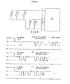
- the switching circuit 7 renders the transistor T 2 conductive. Therefore, a voltage Vq across the lines l 1 and t is dropped to a value V F as determined by the Zener diode Z 2 , as shown in Fig. 4(a), and the thus obtained fire signal is sent to the control panel Re. Accordingly, the voltage drops across the resistor R 8 in the fire signal receiver circuit 25 in the receiver Re, whereby the transistor T 5 is rendered conductive, the monostable multivibrator M l in the timer circuit 36 is operated to energize the timer T through OR circuit OR 1 and to actuate the relay N so that its operation is maintained by the closure of its contact n l .
- outputs of the latch circuit 6 delayed through the delay circuit 8 drive the non-stable multivibrator 11 via inhibit circuit 9 and OR circuit 10, such that pulse outputs are generated.
- the pulses are counted by the counter 12.
- the decoder 13 operates, whereby the flip-flop circuit that works as latch circuit 14 is set, the inhibit input of the inhibit circuit 9 assumes the high level, the non-stable multivibrator 11 is stopped through the OR circuit 10, the counter 12 is cleared through the OR circuit 15, and the output is sent to the delay circuit 17.
- the transistor T 3 in the switching circuit 16 operates for a short period of time responsive to a pulse output from the multivibrator 11, and the voltage across the lines l 1 and l is dropped to V A as shown in Fig. 4(a), such that the address signal in the form of a pulse produced by the detector D 11 is sent to the receiver Re.
- the transistor T 7 in the circuit 26 which receives address signals and fire detection quantity signals, operates responsive to the pulse and is turned on through the contact n 3 in the AND circuit 28 where the transistor T 8 has already been closed, and a pulse number "1" is counted in the counter 29.
- the contact n 4 in the relay N is switched and the flip-flop circuit 31 is set.
- the value counted by the counter 29 therefore is temporarily stored in the register 33 through AND circuit 32, and "1" is displayed on the numeral display tube of the address indicator circuit 35 through decoder 34, to indicate that the first detector has operated, i.e., to indicate that the fire detector D 11 has operated.
- the timer T which operates after a predetermined period of time has passed produces an output which causes the monostable multivibrator M 2 to operate, and the flip-flop circuit 31 is reset by the pulse, the counter 29 is cleared through the OR circuit 37, and the flip-flop circuit 38 is set.
- outputs of the latch circuit 14 delayed by the delay circuit 17 in the fire detector D 11 drive the non-stable multivibrator 18 so that it will periodically produce pulses having a long pulse width. Responsive to the pulses introduced through the flip-flop circuit 19 and the OR circuit 10, the non-stable multivibrator 11 and the analog-to-digital converter 20 are intermittently actuated.
- the number of pulses generated by the multivibrator 11, i.e., the value counted by the counter 12, and the fire detection quantity of the fire detector portion 2, i.e., the output of the analog-to-digital converter 20, are compared in the digital coincidence circuit 21 which produces an output when the analog quantity produced by the fire detector portion 2 is in agreement with the value counted by the counter 12.
- This output resets the flip-flop circuit 19 through OR circuit 22, stops the non-stable multivibrator 11 through OR circuit 10, and clears the counter 12 through OR circuit 15. Therefore, the non-stable multivibrator 11 produces pulses of a number corresponding to the fire detection quantity of the fire detection portion.
- the flip-flop circuit 19 is set responsive to pulses generated successively from the non-stable multivibrator 18, to actuate the non-stable multivibrator 11 and the analog-to-digital converter 20. Being controlled by the digital coincidence circuit 21, therefore, the pulses are continuously produced by the non-stable multivibrator 11 in a number corresponding to the fire detection quantity of that time. Responsive to the thus produced pulses, the transistor T 3 in the switching circuit 16 operates for short periods of time, such that the voltage across the lines l 1 and A is dropped to V A twice and then thrice as shown in Fig. 4(a).
- fire detection quantity signals are sent to the receiver to indicate that the output of the fire detection portion 2 is increasing, for example, to 2 volts and then 3 volts.
- the transistor T 7 in the circuit 26 which receives address signals and fire detection quantity signals, operates responsive to the pulses, whereby the transistor T 8 in the AND circuit 28 is intermittently rendered conductive twice, the timer circuit 36 is energized, the counter 29 counts the pulse number "2", the counted value is temporarily stored in the register 40 through AND circuit 39, and "2" is displayed on the numeral display tube of the detection quantity indicator circuit 42 via decoder 41, to indicate that the output of 2 volts is produced by the fire detection portion 2 in the fire detector D 11 .
- the monostable multivibrator M 2 is then operated by the output of the timer T which operates after a predetermined time has passed, the counter 29 is cleared through OR circuit 37, and the register 40 is reset through OR circuit 45.
- the fire detection quantity signals are then received by the receiver circuit 26, and "3" is displayed in the detection quantity indicator circuit 42, to indicate that the output produced by the fire detector D 11 has risen to 3 volts.
- the above operation is performed repetitively, and the fire detection quantity produced by the detector D 11 is displayed on the control panel Re with the lapse of time.
- the transistor T 1 in their circuit 5 for detecting line voltage remains non-conductive, the inhibit input of the inhibit circuit 4 assumes the high level, and no output is transmitted from the fire detector circuit 1. Namely the detectors D 12 to D ln remain in the inoperative condition.
- the non-stable multivibrator 11 of the detector is stopped by the output of the decoder 12 under the condition in which two pulses are sent. Therefore, two pulses are sent through the switching circuit 16 as shown in Fig. 4(b).
- n pulses are sent as shown in Fig. 4(c). In the control panel Re, therefore, the pulses are counted by the counter 29, and the address indicator circuit 35 indicates that the second detector or the n-th detector has operated.
- a fire signal receiver circuit 25 (which is not shown) operates to indicate the area where fire has broken out, and the pulse number "1" produced by the detector as an address signal is detected by the circuit which receives address signals and fire detection quantity signals, whereby it is indicated that the first detector has operated. Moreover, the output of the detector is indicated relying upon the fire detection quantity signals that are introduced subsequently.
- a button switch 43 for restoring the control panel Re is depressed for a short period of time, the reset circuit 23 in the detector and the reset circuit 44 in the control panel Re operate; i.e., the detector and the control panel are restored to normal condition.
- ion chambers are employed as the fire detector portion 2 in the above-mentioned embodiment, it is of course allowable to employ a fire detector portion of the photoelectric type which detects the light scattered by the smoke or of the thermal type such as thermistors.
- the invention is constructed and operates as mentioned above. Namely, the invention provides a fire alarm system which is capable of discriminating the operation of a fire detector in an area where a plurality of fire detectors are connected in parallel across the same lines, and which is also capable of detecting the change in the output produced by the detector as a result of the fire.
Landscapes
- Business, Economics & Management (AREA)
- Emergency Management (AREA)
- Physics & Mathematics (AREA)
- General Physics & Mathematics (AREA)
- Fire Alarms (AREA)
- Alarm Systems (AREA)
Abstract
Description
- The present invention relates to a fire alarm system which is capable of detecting, through a receiver, the operation and the change in output of individual fire detectors among a plurality of fire sensors that are arrayed in parallel along the same lines in the same area.
- In conventional fire alarm systems, a plurality of fire detectors are connected in parallel across a pair of lines for every area, and the lines are short-circuited when a physical phenomenon such as heat or smoke caused by fire has reached a predetermined value to transmit fire signals to the control panel. Therefore, the area where fire has broken out could be indicated only roughly by the control panel. In other words, it is not possible to indicate which fire detector has worked or the change of its output, and it is not possible to indicate the burning condition. Namely it is not possible to suitably control equipment for preventing or expelling the smoke, or to suitably control fire extinguishers.
- In view of the above-mentioned situations, the object of the present invention is to provide a fire alarm system according to which, in case a fire detector has operated, fire signals are transmitted to the control panel like the conventional fire detector, and an address signal which indicates the operated fire detector and the change in output of the detector are transmitted to the control panel, such that the area where fire has broken out, the operated fire detector and the change of its output, are indicated by the control panel.
- The fire alarm facility according to an embodiment of the present invention will now be described below in conjunction with Figs. 1 to 3.
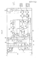
- In Fig. 1, symbols D11 to DIn and Dnl to Dnn denote fire detectors that are connected in parallel across a pair of lines ℓ1 and ℓ through up to a pair of lines ℓn to ℓ covering every area, and Re denotes a control panel. The fire detectors connected in parallel in each area have been constructed in the same way except a decoder that is provided to generate an address signal specific to the detector. Therefore, the detector D11 only will be described below with reference to Figs. 2 and 3, in which
reference numeral 1 denotes a fire detector circuit which consists of afire detector portion 2, and acomparator 3 such as operational amplifier A that detects a predetermined output of thedetector portion 2. Thefire detector portion 2 has an inner ion chamber CH1 and an outer ion chamber CH2 connected in series, and an FET which detects the change in potential at a middle point between the inner ion chamber and the outer ion chamber.Reference numeral 4 denotes an inhibit circuit whose input is connected to the output of thecomparator 3, and whose inhibit input is connected to a line voltage detector circuit 5 which detects a predetermined voltage drop across a pair of lines ℓ1 and ℓ. The detector circuit 5 consists of a transistor T1, a Zener diode Zl, and resistors R1, R2. Under the supervisory condition, the Zener diode Z1 is rendered conductive, whereby the transistor T1 is rendered conductive. When other detectors connected in parallel across the lines ℓ1 and ℓ have worked to decrease the line voltage, the Zener diode Z1 is rendered non-conductive, whereby the transistor T1 becomes non-conductive.Reference numeral 6 denotes a latch circuit consisting of an RS flip-flop circuit, the set terminal being connected to theinhibit circuit 4, and the output terminal being connected to aswitching circuit 7 and to adelay circuit 8. Theswitching circuit 7 is connected across the pair of lines ℓ1, ℓ to produce fire signals, and consists of a Zener diode Z2 having a Zener voltage smaller than that of the Zener diode Z1, and a transistor T2. The base of the transistor T2 which serves as an input terminal is connected to the output of thelatch circuit 6. Thedelay circuit 8 so works that the output of thelatch circuit 6 is produced being delayed by a predetermined period of time, and consists of a resistor R3 and a capacitor C1. The output of thedelay circuit 8 is sent to anon-stable multivibrator 11 via a Schmidt trigger inhibitcircuit 9 and anOR circuit 10. Reference numeral 12 denotes a counter which counts pulse outputs produced by themultivibrator -
Reference numeral 14 denotes a latch circuit which consists of an RS flip-flop circuit, the set terminal thereof being connected to the output of thedecoder 13, and the output terminal thereof being connected to the inhibit input of the inhibit circuit and to a clear terminal of the counter 12 via theOR circuit 15.Reference numeral 16 denotes a switching circuit which is connected across the lines ℓ1 and t like theswitching circuit 7, and which works to send the address and fire detection quantity signal of the detector D11. Theswitching circuit 7 consists of a Zener diode Z3 having a Zener voltage smaller than that of the Zener diode Z2, and a transistor T3, the base of the transistor T3 which serves as an input terminal beinq connected to the output of thenon-stable multivibrator 11.Reference numeral 17 denotes a delay circuit which is connected to the output of thelatch circuit 14, which consists of a resistor R4, a capacitor C2 and a Schmidt triqqer circuit B, and which has a delay time that is sufficiently longer than the time for sending address signals.Reference numeral 18 denotes a non-stable multivibrator which operates responsive to the output of thedelay circuit 17, and which has a pulse width and a period longer than the time for sending the fire detection quantity signals to the control panel Re via themultivibrator 11. The output of thenon-stable multivibrator 18 is connected to thenon-stable multivibrator 11 via a flip-flop circuit 19 and theOR circuit 10.Reference numeral 20 denotes an analog-to-digital converter of which the analog input is connected to the source of the FET in thefire detector portion 2, of which the digital output is supplied to one input of adigital coincidence circuit 21, and of which the strobe input is connected to the output of thenon-stable multivibrator 18. Thedigital coincidence circuit 21 consists of a magnitude comparator, wherein another input for comparison is connected to the output of the counter 12, and the coincidence output is supplied to the clear terminal of the counter 12 via theOR circuit 15, and is also supplied to the reset terminal of the flip-flop circuit 19 viaOR circuit 22.Reference numeral 23 denotes a reset circuit which consists of resistors R5 to R7, a capacitor C3, and a transistor T4, that are provided on the output side of the constant-voltage circuit 24. The collector of the transistor T4 which produces an output is connected to the clear terminal of the counter 12 and to the reset terminal of the flip-flop circuit 19 via theOR circuits latch circuits -
Reference numeral 25 denotes a fire signal receiver circuit in the control panel Re, which consists of resistors R8 to R11, a Zener diode Z4, a transistor T5 which becomes conductive upon receipt of a fire signal from the fire detector, and a self-holding circuit made up of a transistor T6, a relay N, and a contact point nl.Reference numeral 26 denotes a circuit which receives addresses and fire detection quantity signals, and which consists of resistors R8, R12 to R14, a Zener diode Z4, and a transistor T7 which is rendered conductive responsive to a pulse such as an address signal from the fire detector.Reference numeral 27 denotes an alarm indicator circuit which indicates the section where fire has broken out, and which consists of a lamp L that will be turned on when a contact n2 of a relay N is closed.Reference numeral 28 denotes an AND circuit which consists of a contact n3 of a relay N, a transistor T8 of which the base is connected to the collector of the transistor T7, and a resistor R15, that are all connected in series, 29 denotes a counter which counts the number of pulses sent through theAND circuit 28 as address signals and fire detection quantity signals, and which assumes the form of a four-bit binary counter like the counter 12 in the detector, 30 denotes a pulse generator circuit which consists of resistors R16, R17, a capacitor C4 and a contact n4 of a relay N. Thepulse generator circuit 30 is connected to inputs of theAND circuit 32 via a flip-flop circuit 31 together with the output of thecounter 29, such that only the number of pulses in the form of address signals is stored in aregister 33 of a subsequent stage. Further,reference numeral 34 denotes a decoder which converts binary values stored in theregister 33 into different values, e.g., which converts binary numbers into decimal numbers.Reference numeral 35 denotes an address indicator circuit which indicates a detector that is operated by the output of thedecoder 34, and which consists of numeral display tubes.Reference numeral 36 denotes a timer circuit which produces a single pulse after a predetermined period of time has passed from the reception of a fire signal, an address signal or a fire detection quantity signal produced by the fire detector. Thetimer circuit 36 consists of a monostable multivibrator Ml of which the input is connected to the collector of the transistor T5, an OR circuit ORI of which the inputs are connected to the emitter of the transistor T8 and to the output of the vibrator Ml, respectively, a timer T, and a monostable multivibrator M2. The output of thetimer circuit 36 is connected to the clear terminal of thecounter 29 viaOR circuit 37, connected to the reset terminal of the flip-flop circuit 31, and is connected to the set terminal of a flip-flop circuit 38. The output of the flip-flop circuit 38 is connected to the inputs of anAND circuit 39 together with the output of thecounter 29, such that the number of pulses in the form of fire detection quantity signals is temporarily stored in aregister 40 in a subsequent stage. Further,reference numeral 41 denotes a decoder which converts binary numbers stored in theregisters 40 into different values, e.g., which converts binary numbers into decimal numbers, 42 denotes a fire detection quantity indicator circuit which indicates a fire detection quantity depending upon the output of thedecoder 41, and which consists of numeral display tubes, 43 denotes a push-button switch for restoration, and 44 denotes a reset circuit which consits of resistor R18 to R20, a capacitor C5, and a transistor T9. The collector of the transistor T9 which produces output is connected to the flip-flop circuit 38 and to the reset terminal of theregister 33, and is further connected to the clear terminal of thecounter 29 and to the reset terminal of theregister 40, respectively, viaOR circuits OR circuit 45 is connected to the output of thetimer circuit 36. - Operation of the circuit will be described below. In Fig. 2, if smoke produced by fire enters into the ion chamber CH2 in the
fire detector portion 2 of a fire detector D11 among a multiplicity of fire detectors D11 to Dln connected in parallel across the lines ℓ1 and ℓ, the source potential of FET rises, whereby thecomparator 3 operatives at a predetermined value, and the output is sent to theinhibit circuit 4. In this case, other sensors D12 to Dln connected in parallel between the lines ℓ1 and ℓ do not operate, the line voltage detector circuit 5 is inoperative, and the inhibit input of theinhibit circuit 4 assumes the low level. Therefore, the output from thefire detector circuit 1 sets the flip-flop circuit which works as alatch circuit 6 via inhibitcircuit 4, and is further transmitted to theswitching circuit 7 and to thedelay circuit 8. - Responsive to this output, the
switching circuit 7 renders the transistor T2 conductive. Therefore, a voltage Vq across the lines ℓ1 and t is dropped to a value VF as determined by the Zener diode Z2, as shown in Fig. 4(a), and the thus obtained fire signal is sent to the control panel Re. Accordingly, the voltage drops across the resistor R8 in the firesignal receiver circuit 25 in the receiver Re, whereby the transistor T5 is rendered conductive, the monostable multivibrator Ml in thetimer circuit 36 is operated to energize the timer T through OR circuit OR1 and to actuate the relay N so that its operation is maintained by the closure of its contact nl. Consequently, the contact n2 in thealarm indicator circuit 27 is closed to turn the lamp L on. Thus, it is indicated that fire broke out in the area where the de- tectors D11, D12 to Dln are connected in parallel between the lines ℓ1 and ℓ. - Further, while the fire signals are being received by the control panel Re, outputs of the
latch circuit 6 delayed through thedelay circuit 8 drive thenon-stable multivibrator 11 via inhibitcircuit 9 andOR circuit 10, such that pulse outputs are generated. The pulses are counted by the counter 12. When a pulse number "1" is counted, thedecoder 13 operates, whereby the flip-flop circuit that works aslatch circuit 14 is set, the inhibit input of theinhibit circuit 9 assumes the high level, thenon-stable multivibrator 11 is stopped through theOR circuit 10, the counter 12 is cleared through theOR circuit 15, and the output is sent to thedelay circuit 17. Furthermore, the transistor T3 in theswitching circuit 16 operates for a short period of time responsive to a pulse output from themultivibrator 11, and the voltage across the lines ℓ1 and ℓ is dropped to VA as shown in Fig. 4(a), such that the address signal in the form of a pulse produced by the detector D11 is sent to the receiver Re. In the control panel Re, the transistor T7 in thecircuit 26 which receives address signals and fire detection quantity signals, operates responsive to the pulse and is turned on through the contact n3 in theAND circuit 28 where the transistor T8 has already been closed, and a pulse number "1" is counted in thecounter 29. In thepulse generator circuit 30, furthermore, the contact n4 in the relay N is switched and the flip-flop circuit 31 is set. The value counted by thecounter 29 therefore is temporarily stored in theregister 33 through ANDcircuit 32, and "1" is displayed on the numeral display tube of theaddress indicator circuit 35 throughdecoder 34, to indicate that the first detector has operated, i.e., to indicate that the fire detector D11 has operated. Thereafter, the timer T which operates after a predetermined period of time has passed produces an output which causes the monostable multivibrator M2 to operate, and the flip-flop circuit 31 is reset by the pulse, thecounter 29 is cleared through theOR circuit 37, and the flip-flop circuit 38 is set. While the address signals are being received by the control panel Re, outputs of thelatch circuit 14 delayed by thedelay circuit 17 in the fire detector D11 drive thenon-stable multivibrator 18 so that it will periodically produce pulses having a long pulse width. Responsive to the pulses introduced through the flip-flop circuit 19 and theOR circuit 10, thenon-stable multivibrator 11 and the analog-to-digital converter 20 are intermittently actuated. The number of pulses generated by themultivibrator 11, i.e., the value counted by the counter 12, and the fire detection quantity of thefire detector portion 2, i.e., the output of the analog-to-digital converter 20, are compared in thedigital coincidence circuit 21 which produces an output when the analog quantity produced by thefire detector portion 2 is in agreement with the value counted by the counter 12. This output resets the flip-flop circuit 19 throughOR circuit 22, stops thenon-stable multivibrator 11 throughOR circuit 10, and clears the counter 12 throughOR circuit 15. Therefore, thenon-stable multivibrator 11 produces pulses of a number corresponding to the fire detection quantity of the fire detection portion. The flip-flop circuit 19 is set responsive to pulses generated successively from thenon-stable multivibrator 18, to actuate thenon-stable multivibrator 11 and the analog-to-digital converter 20. Being controlled by thedigital coincidence circuit 21, therefore, the pulses are continuously produced by thenon-stable multivibrator 11 in a number corresponding to the fire detection quantity of that time. Responsive to the thus produced pulses, the transistor T3 in the switchingcircuit 16 operates for short periods of time, such that the voltage across the lines ℓ1 and A is dropped to VA twice and then thrice as shown in Fig. 4(a). Thus, fire detection quantity signals are sent to the receiver to indicate that the output of thefire detection portion 2 is increasing, for example, to 2 volts and then 3 volts. In the control panel Re, the transistor T7 in thecircuit 26 which receives address signals and fire detection quantity signals, operates responsive to the pulses, whereby the transistor T8 in the ANDcircuit 28 is intermittently rendered conductive twice, thetimer circuit 36 is energized, thecounter 29 counts the pulse number "2", the counted value is temporarily stored in theregister 40 through ANDcircuit 39, and "2" is displayed on the numeral display tube of the detectionquantity indicator circuit 42 viadecoder 41, to indicate that the output of 2 volts is produced by thefire detection portion 2 in the fire detector D11. The monostable multivibrator M2 is then operated by the output of the timer T which operates after a predetermined time has passed, thecounter 29 is cleared through ORcircuit 37, and theregister 40 is reset through ORcircuit 45. The fire detection quantity signals are then received by thereceiver circuit 26, and "3" is displayed in the detectionquantity indicator circuit 42, to indicate that the output produced by the fire detector D11 has risen to 3 volts. The above operation is performed repetitively, and the fire detection quantity produced by the detector D11 is displayed on the control panel Re with the lapse of time. As for other detectors D12 to Dln connected in parallel across the lines ℓ1 and Q, the transistor T1 in their circuit 5 for detecting line voltage remains non-conductive, the inhibit input of the inhibitcircuit 4 assumes the high level, and no output is transmitted from thefire detector circuit 1. Namely the detectors D12 to Dln remain in the inoperative condition. - When the fire detector D12 has operated instead of the fire detector D11, the
non-stable multivibrator 11 of the detector is stopped by the output of the decoder 12 under the condition in which two pulses are sent. Therefore, two pulses are sent through the switchingcircuit 16 as shown in Fig. 4(b). When the fire detector Dln has operated, n pulses are sent as shown in Fig. 4(c). In the control panel Re, therefore, the pulses are counted by thecounter 29, and theaddress indicator circuit 35 indicates that the second detector or the n-th detector has operated. When a fire detector Dnl of other area has operated, a fire signal receiver circuit 25 (which is not shown) operates to indicate the area where fire has broken out, and the pulse number "1" produced by the detector as an address signal is detected by the circuit which receives address signals and fire detection quantity signals, whereby it is indicated that the first detector has operated. Moreover, the output of the detector is indicated relying upon the fire detection quantity signals that are introduced subsequently. When abutton switch 43 for restoring the control panel Re is depressed for a short period of time, thereset circuit 23 in the detector and thereset circuit 44 in the control panel Re operate; i.e., the detector and the control panel are restored to normal condition. Although ion chambers are employed as thefire detector portion 2 in the above-mentioned embodiment, it is of course allowable to employ a fire detector portion of the photoelectric type which detects the light scattered by the smoke or of the thermal type such as thermistors. - The invention is constructed and operates as mentioned above. Namely, the invention provides a fire alarm system which is capable of discriminating the operation of a fire detector in an area where a plurality of fire detectors are connected in parallel across the same lines, and which is also capable of detecting the change in the output produced by the detector as a result of the fire.
-
- Fig. 1 is a circuit diagram illustrating connections of fire detectors and a control panel in a fire alarm system according to the present invention;
- Fig. 2 is a circuit diagram of a fire detector of Fig. 1;
- Fig. 3 is a circuit diagram of a control panel of Fig. 1; and
- Fig. 4 is a diagram showing voltage waveforms for illustrating the present invention.
- 1 Fire Detector Circuit, 2 Detector portion, 3 Comparator, 4,9 Inhibit Circuit, 5 Line Voltage Detector Circuit, 6,14 Latch Circuit, 7,16 Switching Circuit, 8,17 Delay Circuit, 11,18 Non-Stable Multivibrator, 12,29 Counter, 13,34,41 Decoder, 19 Flip-Flop Circuit, 20 Analog-To-Digital Converter, 21 Digital Coincidence Circuit, 25 Fire Signal Receiver Circuit, 26 Circuit Which Receives Addresses and Fire Detection Quantity Signals, 27 Alarm Indicator Circuit, 28 AND Circuit, 35 Address Indicator Circuit, 42 Fire Detection Quantity Indicator Circuit
- In his letter dated October 29, 1982 which was received by the EPO on November 2, 1982 the Applicant requested that the following corrections of obvious errors made in the originally filed text of the description should be allowed :

- The request for correction is allowed under Rule 88 EPC.
Claims (1)
- A fire alarm system having:fire detectors each of which comprising:a fire detector circuit which detects a predetermined fire detection quantity produced by a fire detector portion such as an ion chamber or a thermistor which detects burning related phenomenon such as smoke or heat;a first inhibit circuit which inhibits the transmission of output from said fire detector circuit when a line voltage of a pair of lines connected to the control panel is dropped;a first latch circuit which stores the output sent from the first inhibit circuit;a first switching circuit which works to decrease the voltage of said line responsive to the operation of the first latch circuit, in order to send a fire signal to the control panel;a first delay circuit which produces an output after a predetermined period of time has passed from the operation of the first latch circuit;a second inhibit circuit which inhibits the transmisssion of output of the first delay circuit responsive to the output of a second latch circuit that will be mentioned below;a first non-stable multivibrator which is operated by the second inhibit circuit;a second switching circuit which is intermittently operated by the output of the first non-stable multivibrator, which is connected across the lines together with said first switching circuit, and which works to decrease the line voltage in order to send an address signal and a signal of fire detection quantity to the receivers;a decoder which generates address signals to detect a predetermined value of a counter that counts the outputs of the first non-stable multivibrator;a second latch circuit which stores the output of the decoder;a second delay circuit which produces an output after a predetermined period of time has passed responsive to the operation of the second latch circuit;a second non-stable multivibrator which operates responsive to the output of the second delay circuit;an analog-to-digital converter which converts analog outputs into digital values, said analog outputs being produced by a flip-flop circuit which is set by the second non-stable multivibrator and which actuates said first non-stable multivibrator, and said analog outputs being further produced by the fire detection portion; anda digital coincidence circuit which compares the output of the converter with the output of said counter, and stops said first non-stable multivibrator when said outputs are in agreement;and a control panel comprising:a fire signal receiving circuit which detects a predetermined line voltage dropped by the operation of the first switching circuit in the fire detector;a circuit for receiving addresses and fire detection quantity signals that are produced by the second switching circuit in the fire detector;an AND circuit which permits the passage of the circuit that receives addresses and fire detection quantity signals, responsive to the operation of said fire signal receiving circuit;a counter which counts the pulse outputs of said AND circuit;decoders which detect the counter values and which indicate addresses and fire detection quantities; anda display circuit.
Applications Claiming Priority (2)
| Application Number | Priority Date | Filing Date | Title |
|---|---|---|---|
| JP102305/81 | 1981-07-02 | ||
| JP10230581A JPS585896A (en) | 1981-07-02 | 1981-07-02 | Fire alarm facility |
Publications (2)
| Publication Number | Publication Date |
|---|---|
| EP0071752A1 true EP0071752A1 (en) | 1983-02-16 |
| EP0071752B1 EP0071752B1 (en) | 1986-12-10 |
Family
ID=14323888
Family Applications (1)
| Application Number | Title | Priority Date | Filing Date |
|---|---|---|---|
| EP19820105866 Expired EP0071752B1 (en) | 1981-07-02 | 1982-07-01 | Fire alarm system |
Country Status (3)
| Country | Link |
|---|---|
| EP (1) | EP0071752B1 (en) |
| JP (1) | JPS585896A (en) |
| DE (1) | DE3274690D1 (en) |
Cited By (5)
| Publication number | Priority date | Publication date | Assignee | Title |
|---|---|---|---|---|
| EP0167669A1 (en) * | 1984-06-05 | 1986-01-15 | Siemens Aktiengesellschaft | Method of and device for identifying an alarm triggering sensor in a danger signalling device |
| WO1997020295A1 (en) * | 1995-11-28 | 1997-06-05 | Rolf Edman | A controlling and/or registration system |
| GB2321747A (en) * | 1997-01-30 | 1998-08-05 | Rafiki Protection Limited | Fire alarm system |
| US8094030B2 (en) | 2006-02-24 | 2012-01-10 | Airbus Operations Sas | Fire detection system and aircraft equipped with such a system |
| CN104008625A (en) * | 2014-05-21 | 2014-08-27 | 关宏 | Intelligent fire evacuation system achieving evacuation through images |
Families Citing this family (4)
| Publication number | Priority date | Publication date | Assignee | Title |
|---|---|---|---|---|
| JPS6065398A (en) * | 1983-09-20 | 1985-04-15 | ホーチキ株式会社 | Fire alarm |
| JPS59214997A (en) * | 1983-05-20 | 1984-12-04 | ニツタン株式会社 | Fire alarm |
| JPS6019299A (en) * | 1983-07-14 | 1985-01-31 | 沖電気防災株式会社 | Alarm signal system |
| JPS6154596A (en) * | 1984-08-25 | 1986-03-18 | 松下電工株式会社 | Fire self-alarm system |
Citations (4)
| Publication number | Priority date | Publication date | Assignee | Title |
|---|---|---|---|---|
| FR2111743A1 (en) * | 1970-10-21 | 1972-06-09 | Preussag Ag Feuerschutz | |
| DE2261179A1 (en) * | 1972-12-14 | 1974-06-20 | Preussag Ag Feuerschutz | NOTIFICATION DEVICE, IN PARTICULAR FOR FIRE NOTIFICATION |
| US4162483A (en) * | 1977-04-01 | 1979-07-24 | Intech Laboratories, Inc. | Bilateral master station-plural satellite station signalling apparatus |
| GB2030336A (en) * | 1978-09-06 | 1980-04-02 | Wolsey Emergency Audio Communi | Improvements Relating to Emergency Alarm Systems |
-
1981
- 1981-07-02 JP JP10230581A patent/JPS585896A/en active Granted
-
1982
- 1982-07-01 DE DE8282105866T patent/DE3274690D1/en not_active Expired
- 1982-07-01 EP EP19820105866 patent/EP0071752B1/en not_active Expired
Patent Citations (4)
| Publication number | Priority date | Publication date | Assignee | Title |
|---|---|---|---|---|
| FR2111743A1 (en) * | 1970-10-21 | 1972-06-09 | Preussag Ag Feuerschutz | |
| DE2261179A1 (en) * | 1972-12-14 | 1974-06-20 | Preussag Ag Feuerschutz | NOTIFICATION DEVICE, IN PARTICULAR FOR FIRE NOTIFICATION |
| US4162483A (en) * | 1977-04-01 | 1979-07-24 | Intech Laboratories, Inc. | Bilateral master station-plural satellite station signalling apparatus |
| GB2030336A (en) * | 1978-09-06 | 1980-04-02 | Wolsey Emergency Audio Communi | Improvements Relating to Emergency Alarm Systems |
Cited By (6)
| Publication number | Priority date | Publication date | Assignee | Title |
|---|---|---|---|---|
| EP0167669A1 (en) * | 1984-06-05 | 1986-01-15 | Siemens Aktiengesellschaft | Method of and device for identifying an alarm triggering sensor in a danger signalling device |
| WO1997020295A1 (en) * | 1995-11-28 | 1997-06-05 | Rolf Edman | A controlling and/or registration system |
| GB2321747A (en) * | 1997-01-30 | 1998-08-05 | Rafiki Protection Limited | Fire alarm system |
| GB2321747B (en) * | 1997-01-30 | 2000-10-18 | Rafiki Protection Limited | Alarm system |
| US8094030B2 (en) | 2006-02-24 | 2012-01-10 | Airbus Operations Sas | Fire detection system and aircraft equipped with such a system |
| CN104008625A (en) * | 2014-05-21 | 2014-08-27 | 关宏 | Intelligent fire evacuation system achieving evacuation through images |
Also Published As
| Publication number | Publication date |
|---|---|
| JPS6355120B2 (en) | 1988-11-01 |
| DE3274690D1 (en) | 1987-01-22 |
| JPS585896A (en) | 1983-01-13 |
| EP0071752B1 (en) | 1986-12-10 |
Similar Documents
| Publication | Publication Date | Title |
|---|---|---|
| US4613848A (en) | Multiple-zone intrusion detection system | |
| US4638304A (en) | Environmental abnormality detecting apparatus | |
| GB2169401A (en) | Light-attenuation type fire detector assembly | |
| EP0071752A1 (en) | Fire alarm system | |
| JPS63251897A (en) | Environment abnormality alarm | |
| JPS6014399B2 (en) | Physical change monitoring device | |
| EP0088524A1 (en) | Intruder alarm system | |
| US4744038A (en) | Fire detector equipped with a sensor | |
| CA1129034A (en) | Smoke detector | |
| US5850178A (en) | Alarm system having synchronizing pulse generator and synchronizing pulse missing detector | |
| US4455549A (en) | Indication device | |
| US4498074A (en) | Selectively testable fire detector | |
| US4881060A (en) | Fire alarm system | |
| EP0367486B1 (en) | Fire alarm system | |
| US4544921A (en) | Fire alarm system | |
| US4151472A (en) | Selective calling circuit employing controlled power supply therefor | |
| US4506161A (en) | Smoke detector with a radiation source operated in a pulse-like or intermittent mode | |
| EP0205749B1 (en) | Fire alarm system | |
| JPS5927395A (en) | Alarm | |
| JPH0341879B2 (en) | ||
| DK155387B (en) | PROCEDURE AND APPARATUS FOR AUTOMATICALLY INQUIRY OF THE ALTERNATIVE VALUE AND THE ALERT RECOGNITION IN A DANGER ALARMING SYSTEM | |
| US3430199A (en) | Teleidentification system for monitoring a plurality of points | |
| US4665384A (en) | Signal-transmitting junction unit of hazard alarm system | |
| US4721953A (en) | Remote control system | |
| US3628142A (en) | Sliding interval event detector |
Legal Events
| Date | Code | Title | Description |
|---|---|---|---|
| PUAI | Public reference made under article 153(3) epc to a published international application that has entered the european phase |
Free format text: ORIGINAL CODE: 0009012 |
|
| 17P | Request for examination filed |
Effective date: 19821115 |
|
| AK | Designated contracting states |
Designated state(s): BE CH DE FR GB IT LI SE |
|
| ITF | It: translation for a ep patent filed |
Owner name: VETTOR GALLETTI DI SAN CATALDO |
|
| GRAA | (expected) grant |
Free format text: ORIGINAL CODE: 0009210 |
|
| AK | Designated contracting states |
Kind code of ref document: B1 Designated state(s): BE CH DE FR GB IT LI SE |
|
| REF | Corresponds to: |
Ref document number: 3274690 Country of ref document: DE Date of ref document: 19870122 |
|
| ET | Fr: translation filed | ||
| PLBE | No opposition filed within time limit |
Free format text: ORIGINAL CODE: 0009261 |
|
| STAA | Information on the status of an ep patent application or granted ep patent |
Free format text: STATUS: NO OPPOSITION FILED WITHIN TIME LIMIT |
|
| 26N | No opposition filed | ||
| REG | Reference to a national code |
Ref country code: CH Ref legal event code: PFA Free format text: NOHMI BOSAI LTD |
|
| ITTA | It: last paid annual fee | ||
| EAL | Se: european patent in force in sweden |
Ref document number: 82105866.6 |
|
| PGFP | Annual fee paid to national office [announced via postgrant information from national office to epo] |
Ref country code: FR Payment date: 19950612 Year of fee payment: 14 |
|
| PGFP | Annual fee paid to national office [announced via postgrant information from national office to epo] |
Ref country code: GB Payment date: 19950616 Year of fee payment: 14 |
|
| PGFP | Annual fee paid to national office [announced via postgrant information from national office to epo] |
Ref country code: SE Payment date: 19950619 Year of fee payment: 14 |
|
| PGFP | Annual fee paid to national office [announced via postgrant information from national office to epo] |
Ref country code: DE Payment date: 19950620 Year of fee payment: 14 |
|
| PGFP | Annual fee paid to national office [announced via postgrant information from national office to epo] |
Ref country code: BE Payment date: 19950622 Year of fee payment: 14 |
|
| PGFP | Annual fee paid to national office [announced via postgrant information from national office to epo] |
Ref country code: CH Payment date: 19950630 Year of fee payment: 14 |
|
| PG25 | Lapsed in a contracting state [announced via postgrant information from national office to epo] |
Ref country code: GB Effective date: 19960701 |
|
| PG25 | Lapsed in a contracting state [announced via postgrant information from national office to epo] |
Ref country code: SE Effective date: 19960702 |
|
| PG25 | Lapsed in a contracting state [announced via postgrant information from national office to epo] |
Ref country code: LI Effective date: 19960731 Ref country code: CH Effective date: 19960731 Ref country code: BE Effective date: 19960731 |
|
| BERE | Be: lapsed |
Owner name: NOHMI BOSAI KOGYO CO. LTD Effective date: 19960731 |
|
| GBPC | Gb: european patent ceased through non-payment of renewal fee |
Effective date: 19960701 |
|
| REG | Reference to a national code |
Ref country code: CH Ref legal event code: PL |
|
| PG25 | Lapsed in a contracting state [announced via postgrant information from national office to epo] |
Ref country code: FR Effective date: 19970328 |
|
| PG25 | Lapsed in a contracting state [announced via postgrant information from national office to epo] |
Ref country code: DE Effective date: 19970402 |
|
| EUG | Se: european patent has lapsed |
Ref document number: 82105866.6 |
|
| REG | Reference to a national code |
Ref country code: FR Ref legal event code: ST |