EP0055741B1 - Input/output system and method of communication for peripheral devices in data processing system - Google Patents
Input/output system and method of communication for peripheral devices in data processing system Download PDFInfo
- Publication number
- EP0055741B1 EP0055741B1 EP81901997A EP81901997A EP0055741B1 EP 0055741 B1 EP0055741 B1 EP 0055741B1 EP 81901997 A EP81901997 A EP 81901997A EP 81901997 A EP81901997 A EP 81901997A EP 0055741 B1 EP0055741 B1 EP 0055741B1
- Authority
- EP
- European Patent Office
- Prior art keywords
- message
- peripheral
- processor
- sccp
- information
- Prior art date
- Legal status (The legal status is an assumption and is not a legal conclusion. Google has not performed a legal analysis and makes no representation as to the accuracy of the status listed.)
- Expired
Links
Images


Classifications
-
- G—PHYSICS
- G06—COMPUTING; CALCULATING OR COUNTING
- G06F—ELECTRIC DIGITAL DATA PROCESSING
- G06F13/00—Interconnection of, or transfer of information or other signals between, memories, input/output devices or central processing units
- G06F13/38—Information transfer, e.g. on bus
- G06F13/382—Information transfer, e.g. on bus using universal interface adapter
- G06F13/385—Information transfer, e.g. on bus using universal interface adapter for adaptation of a particular data processing system to different peripheral devices
-
- G—PHYSICS
- G06—COMPUTING; CALCULATING OR COUNTING
- G06F—ELECTRIC DIGITAL DATA PROCESSING
- G06F13/00—Interconnection of, or transfer of information or other signals between, memories, input/output devices or central processing units
- G06F13/14—Handling requests for interconnection or transfer
- G06F13/20—Handling requests for interconnection or transfer for access to input/output bus
- G06F13/22—Handling requests for interconnection or transfer for access to input/output bus using successive scanning, e.g. polling
Landscapes
- Engineering & Computer Science (AREA)
- Theoretical Computer Science (AREA)
- Physics & Mathematics (AREA)
- General Engineering & Computer Science (AREA)
- General Physics & Mathematics (AREA)
- Communication Control (AREA)
Abstract
Description
- This invention relates to an input/output system and method of communication for peripheral devices in a data processing system.
- This application is related to an international application filed by the present Applicants on the same day as the present application entitled "Input/Output Processor and Method of Communication for Data Processing System"; cf. WO 82/00374 (EP-A-81902109.8).
- Where it is desired to connect a multiplicity of peripheral devices in a data processing system, as for example a multi-user system, various techniques such as polling, interrupts, direct memory access and message switching (see "Instruction to Operating System Design", A. N. Haber- mann-SRA-1976) have been employed in an effort to provide an efficient means of communication between the peripheral devices and the main memory and central processor.
- U.S. Patent 4,079,452 discloses a means of coupling a large number of peripheral devices having various communications protocols to a data processor, comprising connecting groups of peripheral devices to respective interface adapters, and connecting the interface adapters in parallel to a programmer controller module, the controller module being coupled via a direct memory access module to a data processor. The controller module includes a special purpose computer having a program of subroutines for implementing the specific communications protocols.
- The problem with such a means of communication is that it is not sufficiently flexible nor of sufficient capacity to handle the high data flow requirements of a large and fast main frame data processing system which may have among other features several central processor elements.
- From US-A-4200930 there is known a data processing system having a plurality of processing elements, a central memory coupled to said processing elements, and an I/O processor coupled to the central memory, the I/0 processor having a plurality of channel ports for communicating information to a plurality of peripheral subsystems, and each peripheral subsystem including a peripheral adapter interfacing with a plurality of peripheral devices.
- From IBM Technical Disclosure Bulletin,
Volume 21, No. 7, December 1978, pages 2633-2645, there is known a data processing system having a processing element, a central memory coupled to the processing element, and an I/O processor coupled to the central memory, the I/0 processor having a plurality of scanner lines and a controller incorporating a microprocessor. The system also includes an interrupting resource for interrupt preparation of the I/0 processor. - From US-A-4016548 there is known a communications multiplier module which assembles serial-by-bit data from a plurality of input ports into parallel-by-bit characters before transmitting them to a host computer.
- It is an object of the invention to provide a means of communicating between a multiplicity of peripheral devices and a data processing system, said means having a flexibility which enables said means to be capable of efficient operation under high rates of data flow.
- According to the invention there is provided a data processing system having at least one processing element, a central memory coupled to said processing element, and an I/O processor coupled to said central memory, and wherein said I/O processor has channel port means for providing transmission paths for communicating information to a plurality n of peripheral subsystems and wherein each of said peripheral subsystems has included a'peripheral adapter inferfacing with a plurality of peripheral devices, characterized in that said I/O processor has a plurality m of serial channel control processors, where n is greater than m, and dynamic channel exchange means which includes a plurality n of bit serial channel ports for providing a transmission path in a bit serial link format to each of said peripheral subsystems and which allows a said serial channel control processor to communicate with any one of the peripheral adapters, and in that each said peripheral adapter comprises first means having an input adapted to receive information from said 1/0 processor and having an output adapted to transmit information to said 1/0 processor, for performing a serial-to-parallel or parallel-to-serial transformation on the information from said 1/0 processor or to said l/O processor, respectively, second means, having a plurality of input-output terminals adapted to interface with said peripheral devices, for providing peripheral controller logic functions for controlling said peripheral devices, and for the transfer of information with said peripheral devices, and third means, operatively connected to said first means and to said second means, for generating response transmission to said 1/0 processor in accordance with a defined message protocol, in conjunction with controlling the transfer of information between said first means and said second means.
- By providing a data system in accordance with the present invention wherein data communications between the peripheral devices and the 1/0 processor are carried out in accordance with a message protocol by means of a peripheral adapter, there can be achieved a speedy and efficient method of communication which can deal with high transmission rates.
- One embodiment of the invention will now be described by way of example with reference to the accompanying drawings, in which:
- Fig. 1 is a block diagram of a data processing system having a preferred structure;
- Fig. 2 depicts the format of the central memory I/O tast structure;
- Fig. 3 is a block diagram showing the switchable data paths through a dynamic channel exchange;
- Fig. 4 is a block diagram of the peripheral adapter according to the invention;
- Fig. 5 is a block diagram of the message protocol module of the peripheral adapter;
- Figs. 6A and 6B are a flowchart illustrating the operation of the system;
- Fig. 6C shows the relationship of Figs. 6A and 6B;
- Fig. 7 depicts a typical message sequence;
- Fig. 8 shows the message formats;
- Fig. 9 shows the command messages in a typical data output sequence;
- Fig. 10 shows the command messages in a typical data input sequence; and
- Fig. 11A through 11E is a flow diagram of the microinstruction sequences of the message protocol module.
- Referring to Fig. 1, the data processing system includes an Input/Output Subsystem (IOSS)1. The IOSS
architecture 1 comprises the I/O Task Structure (IOTS) shown as thecentral memory 10, the serial channel control processors (SCCPs) 20, the dynamic channel exchange (DCX) 21, and includes theperipheral subsystems peripheral devices 41A-41G. In a data processing system, at least one processing element, 22, 22' is coupled to thecentral memory 10. TheSCCPs 20 and the DCX 21 together form what is more generally known as an I/O processor 23, the 1/0 processor being coupled to thecentral memory 10. The coupling of the IOSS elements is shown in Fig. 1 utilizing aninternal transfer bus 24, although it will be understood by those skilled in the art that any standard coupling means may be used. TheDCX 21 interfaces with theperipheral subsystems 30 utilizing bitserial channels 32 connected toperipheral adapters 40 by bitserial lines 31. - The message protocol module is an element of a
peripheral adapter 40. A message protocol is defined for the transmission of information between theprocessing element 22 and theperipheral devices 41A-41G. The message protocol module is implemented to generate the control signal sequences required to effect the peripheral device information transfer in accordance with the defined protocol. The implementation is achieved by the use of a ROM and associated control logic within aperipheral adapter 40 and will be described hereinafter. - The serial
channel control processors 20 form part of the l/O processor 23. TheSCCPs 20 form the overall 1/0 controller of the data processing system and interface with theperipheral adapters 40 for peripheral device information transfer, theSCCPs 20 performing the various control, transmission initiation, and termination functions in accordance with the defined protocol. The SCCP functions are implemented in the SCCP 20 utilizing a ROM and associated control logic, which is more fully described in the aforementioned co-pending application. - Before describing the overall IOSS sysmem operation, it will be advantageous to give a brief description of the individual elements of the IOSS system. Referring to Fig. 2, the 1/0 task structure (IOTS) of
central memory 10 is a memory resident set of tables and lists, denoted herein as 1/0 Field (IOF), that permit communication between the 1/0 software of the processing element orelements 22, 22' and the serialchannel control processors 20. The tables and lists of the IOTS ofcentral memory 10 make up the control information utilized bySCCPs 20. The Peripheral Address Fields (PAFs) indicate the specific peripheral to be addressed, and the function to be performed; the number of PAF bytes of the preferred embodiment can be as many as twelve depending on theperipheral subsystems 30. The Starting Memory Address specifies thecentral memory 10 starting location of the data to be transmitted or received, the Total Byte Count indicates the number of words to be transmitted or received, and the Final Byte Count indicates the number of bytes transmitted at the end of a transfer sequence. The C field is utilized to check that an SCCP is communicating with the correct peripheral. The Status word is utilized to indicate the current state of the communication. - Referring to Fig. 3, the
DCX 21 is shown interfacing withSCCPs 20 through standardinterface SCCP ports 34, and interfacing theperipheral subsystems 30 through bitserial channels 32 via bitserial lines 31. There are m-SCCP ports 34 and n-bit serial channels (BSC) 32, with the number m being less than the number n. In the preferred embodiment, m is four and n is eight, expandable up to 8 and 32 respectively. TheSCCP ports 34 and the bitserial channels 32 each connect to theswitching logic 35. Theswitching logic 35 thereby allows an SCCP 20 to communicate with anyperipheral adapter 40 by providing a data path between theSCCP 20 and the desiredperipheral adapter 40. - A
peripheral subsystem 30 includes aperipheral adapter 40 and at least oneperipheral device 41. Eachperipheral adapter 40 of the IOSS performs the controller function for the associated peripheral device(s) 41 exchanging the control messages and data with anSCCP 20 in accordance with the defined message protocol. The message exchanges of aperipheral adapter 40 are implemented by the use of a ROM and associated control logic which is more fully described hereinunder. - The serial
channel control processors 20 are small device-independent processors used to control the input and output of data between aprocessing element 22 and theperipheral subsystems 30. Still referring to Fig. 3, theSCCPs 20 communicate with the I/O software of theprocessing element 22 via the I/O task structure ofcentral memory 10 and theinternal transfer bus 24. EachSCCP 20 occupies one bus position on theinternal transfer bus 24 and is connected to an associatedSCCP port 34 of theDCX 21. AnSCCP 20 can request communication to any bitserial channel 32 through switchinglogic 35 ofDCX 21, but the requestingSCCP 20 may connect to and control only oneBSC 32 at a time. Thus, the services between all the BSCs 32 are time shared, thereby permitting anSCCP 20 to control the I/O transfer between aprocessing element 22 and aperipheral subsystem 30. The control functions of theSCCPs 20 are described in detail in the aforementioned co-pending application. - Data transmission is via bit
serial channels 32 at a fixed transmission speed, the transmission speed utilized in the preferred embodiment being sixteen megabits per second (two megabytes per second). Transmission between the SCCPs 20 and theperipheral adapters 40, via theDCX 21, is independent of the transfer rate of theperipheral subsystems 30 or of thecentral memory 10. The SCCPs 20 and theperipheral adapters 40 ofperipheral subsystems 30 contain buffers to facilitate this isolation. Communications over the BSC lines 31 is message oriented, so as to comply with a defined message protocol and a defined transmission protocol. In the preferred embodiment, up to 256, 8-bit bytes of data can be transferred in one direction as a block.BSC 32 connections are ordinarily maintained betweenSCCPs 20/DCX 21 as long as information transfer is occurring. By polling theBSCs 32 when no I/O transmissions are taking place, theSCCPs 20/DCX 21 are available to serve a waitingperipheral subsystem 30. In this way maximum bitserial channel 32 utilization is achieved and asmultiple SCCPs 20 are available, load sharing is accomplished. The SCCPs 20/DCX 21 are peripheral independent and therefore can serve anyperipheral subsystem 30. 1/0 system bandwidth can be increased by adding additional SCCPs 20. - Referring to Fig. 4, a block diagram of a
peripheral adapter 40 is shown comprising a link control module (LCM) 401, coupled to the message control module (MPM) 402, which in turn is coupled to the peripheral adapter (PA)nucleus 403. TheLCM 401 interfaces with the 1/0processor 23 via a bitserial line 31 and performs the bit-to-byte or byte-to-bit translation. ThePA nucleus 403 interfaces with aperipheral device 41 and comprises a data buffer and the logic for controlling the functions of theperipheral device 41. Peripheral controller logic functions are well known by those skilled in the art; hence, the functions are not discussed herein. The data buffer ofPA nucleus 403 provides for isolating the peripheral device transfer rate from theBSC 32 transfer rate. Themessage protocol module 402 generates and receives control signals to and from thePA nucleus 403 for controlling the 1/0 with aprocessing element 22, the control being administered by interfacing with anSCCP 20 in accordance with the defined message protocol. - Referring to Fig. 5, a block diagram of the
MPM 402 is shown. - A
sequence controller 410 provides the overall control ofMPM 402. Thesequence controller 410 comprises, in part, a ROM, a ROM sequencer, and a state register, not shown. The ROM sequencer causes the micro-instructions of the ROM to be executed, the execution of the microinstructions generating the control signals such that theMPM 402 can perform a defined operation. The ROM is configured such that the microinstruction words perform the defined operations upon execution, the defined operations being responses to anSCCP 20 in accordance with the defined message protocol which will be described hereinunder. The ROM sequencer is well known by those skilled in the art and will not be discussed further here.Sequence controller 410 interfaces with theLCM 401 for receiving a message control byte. Logic within thesequence controller 410 operates to initiate a branch to the appropriate routine stored within the ROM, based on the configuration of the state register and the message control byte of the message receive. Command and results inputs which are transferred between a CS-RAM 420 andcentral memory 10, are controlled by thesequence controller 410. Data transfers between thePA nucleus 403 andcentral memory 10 are also controlled by thesequence controller 410. - The Service Information Control Interface (SICI) 430 provides the interface control to the
PA nucleus 403. The SICI also providessequencer controller 410 timing and CS-RAM 420 timing.SICI 430 also interfaces withLCM Interface Logic 440 for transferring various control signals between theLCM 401 and thePA nucleus 403. A PA nucleus service request signal received from thePA nucleus 403 is transferred to theLCM 401 viaLCM Interface Logic 440 causing theLCM 401 to transmit a Service Needed signal to anSCCP 20 which will be discussed in detail hereinunder. TheSICI 430 also provides data read and write signals to thePA nucleus 403 for reading from or writing into the PA nucleus data buffer. An interrupt to thePA nucleus 403 is also provided to indicate a transmission sequence, which was prompted by thePA nucleus 403, is properly completed. A transmission sequence includes the transfer of data or the transfer of status, and will be described in detail hereinunder. - The command Status RAM (CS-RAM) 420 is a read-write scratchpad memory for providing temporary storage. Information required by a
PA 40 to communicate with anSCCP 20 in accordance with the defined message protocol is stored in CS-RAM 420. The CS-RAM 420 serves as an information exchange point between thesequence controller 410 and thePA nucleus 403. The CS-RAM 420 is organized to store the command and control information, including the PAFs, received from anSCCP 20. The CS-RAM stores peripheral service type information received fromPA nucleus 403, including a data output ready indication, data input ready indication, results input ready indication, and information to be contained in the service setup information field of the literal appended message discussed hereinunder. The CS-RAM also stores the peripheral status information received fromPA nucleus 403, including peripheral ready, peripheral busy, or peripheral absent indications. - The CS-
RAM Control Logic 450 provides the administering and multiplexing of CS-RAM address and data between thesequence controller 410 and thePA nucleus 403. Access to the CS-RAM 420 is divided equally between thesequence controller 410 and thePA nucleus 403 by a timing control signal. When the timing control signal is in a first state, the sequence controller can read or write data in the CS-RAM 420. When the timing control signal is in a second state, thePA nucleus 403 can read or write data in the CS-RAM 420. Separate CS-RAM address counters and data registers are provided for thesequence controller 410 and thePA nucleus 403 so that continuity of address and data is maintained for both elements with the multiplexing scheme. - The
LCM interface logic 440 contains the logic for providing the handshake control to pass serial bytes betweenLCM 401 andMPM 402 and betweenLCM 401 and the data buffer of thePA nucleus 403. An End of Message signal from theLCM 401 is a control signal inputted to theMPM 402 via theLCM interface logic 410 indicating the termination of a transmission sequence from anSCCP 20. - The systems operation will now be described with the aid of the flowcharts of Figs. 6A and 6B taken together as shown by Fig. 6C. Figs. 6A and 6B show a generalized function flow of the operations performed by the individual elements, namely a
processing element 22, anSCCP 20, aperipheral adapter 40, and aperipheral device 41, in the overall 1/0 operation, the dotted lines indicating "control type" information transferred between elements. - When a
processor element 22 desires to communicate to a peripheral 41, the Process Initiate I/ 0 routine (block 600) of the 1/0 software of theprocessor element 22 is executed which creates the 1/0 fields (IOF) and places these fields within the I/O task structure of central memory 10 (block 601), the l/O task structure being an area ofcentral memory 10 allocated for storing the lists and tables utilized in performing the l/O function in accordance with the defined message protocol. After the 1OFs and the data to be transferred to the peripheral 41 are stored within the proper locations ofcentral memory 10, a message is sent to SCCP 20 (block 605) which indicates a check of the IOF ofcentral memory 10 is to be performed (dotted line from block 605), thePE 22 continuing to execute its assigned task. Theprocessor element 22 plays no further role in the transfer of information betweencentral memory 10 and the relevantperipheral adapter 40. The 1/0 software ofPE 22 reads the status word of the l/O task structure when the data transfer is complete (block 610), the l/O completion indicated to the I/0 software via a message from theSCCP 20 or the I/ O software times out the 1/0 if no termination has occurred. If the status signifies that the data transfer is completed, the next data transfer with that peripheral can be set up and initiated. If the status indicates an incomplete or a busy, a retry may be attempted or some other appropriate action may be taken by the l/O software. - When no 1/0 transmission are taking place, an
SCCP 20 is an interrogation loop (block 620) testing for a Check IOF (CIOF) message from PE 20 (dotted line from block 605) or a Service Needed (SN) message (dotted line from block 670). When an input is received, the SCCP determines the specific request (block 625). (Assume for the present that a "Check IOF" message was received from PE 20). When a check IOF message is received by theSCCP 20, the lOFs are read from central memory 10 (block 630). (The data contained in the 1OFs is used bySCCP 20 to instruct theDCX 21 to connect the appropriate BSC 32). TheSCCP 20 then passes initiating command (or enabling) information (block 635) to the peripheral adapter 40 (dotted line from block 635) in accordance with the defined message protocol which is described in detail hereinunder. Theperipheral adapter 40 responds to theSCCP 20 that the initiating command was received (dotted line from block 660). TheSCCP 20 waits a specified amount of time for the response from theperipheral adapter 40 that the initiating (or enabling) command was received (block 640). The initial command transfer performed betweenCM 10 andPA 40 includes the transfer of command information (i.e., the command appended message exchange to be described in detail hereinunder) required by thePA 40 to properly communicate with anySCCP 20 which might subsequently service thePA 40 to handle the actual data exchange message sequence. When the initial transfer sequence is complete, theSCCP 20 disconnects from thePA 40, status information is stored in central memory 10 (block 650) and theSCCP 20 returns to interrogating loop (block 620). If theperipheral adapter 40 is busy or does not respond, theSCCP 20 stores the busy status in the appropriate location of the IOF and the transmission is terminated (block 650). TheSCCP 20 then returns to the interrogating loop (block 620). After the initial transfer sequence, theSCCP 20 responds to the service needed indication. For output transfers (from the PE 22) initiated by thePE 22, theperipheral adapter 40 sends service needed after theperipheral device 41 has completed the command operation (e.g., slewing or skipping) specified in the initial transfer sequence. - When the
peripheral device 41 desires to communicate to thecentral memory 10, the peripheral indicates this by informing the peripheral adapter (dotted line from block 695) which may be by an interrupt, a signal line, etc., the indication being a function of the peripheral 41. - When no I/O transmissions are taking place, the peripheral adapter is essentially in an idle mode, depicted by
block 680, as being in a loop awaiting a transmission initiation request. When the transmission initiation request is received theperipheral adapter 40 determines the request is from the peripheral device (PER) (block 690), and if the peripheral adapter had been previously enabled (block 675), a Service Needed message is sent (block 670) to aBSC 32 ofDCX 21. During quiescent periods, theSCCPs 20poll BSCs 32 for Service Needed. Thefirst SCCP 20 to poll that BSC will service the peripheral adapter. In this manner theSCCP 20 receives the Service Needed message (dotted line from block 670). TheSCCP 20 detects the Service Needed and indicates to thePA 40 that theSCCP 20 is ready (block 655), dotted line from (block 655) and proceeds to transfer information in accordance with the defined message protocol (block 645). Meanwhile, upon receipt that theSCCP 20 is ready (block 665) thePA 40 proceeds to its transfer counterpart (block 660) and begins the transfer of information betweencentral memory 10 and the peripheral adapter 40 (block 660) in accordance with the defined message protocol. When the transfer is completed (block 685), theperipheral adapter 40 enters the idle state (block 680). When the transmission initiation request is from theSCCP 20, theperipheral adapter 40 makes that determination (block 690) and proceeds to transfer information in accordance with the defined message protocol (block 660). The SCCP initiated transmission request includes the enabling command which may not be followed by any subsequent information transfer from theSCCP 20. Theperipheral adapter 40 then returns to the idle loop (block 680) in accordance with the defined message protocol. - A message protocol is defined for the orderly transfer of information between the SCCPs 20 and the
peripheral adapters 40. AnSCCP 20 can initiate an information transfer to aperipheral adapter 40 by issuing an appropriate control message. The message protocol, as defined, does not allow aperipheral adapter 40 to initiate an information transfer to the central system (i.e., to an SCCP 20). (A data processing system comprising thecentral memory 10, processingelements 22, and the 1/0processor 23, is sometimes referred to herein as the central system), Aperipheral adapter 40 must wait for a command from anSCCP 20 before it can transfer information. The information transfer is on a transmit-response basis. AnSCCP 20 issues a message to aperipheral adapter 40 and waits for a response from theperipheral adapter 40 before issuing another message. Aperipheral adapter 40 issues a message only in response to a received message. Recovery procedures are defined within the message protocol of the preferred embodiment to allow for the retransmission of any message found to be in error. Error sequences are not described herein. Many alternative approaches to error sequences, which include retry, recovery, etc., are well known and may be implemented by those skilled in the art without departing from the true spirit of the invention. - The defined message protocol is message oriented. The basic unit of information grouping is a message, the message being the vehicle for every command, every response, and all information that is transmitted. Referring to Fig. 7, a typical message sequence is depicted. A message sequence is initiated by an
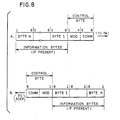
SCCP 20 by transmitting a sequence starting message to which theperipheral adapter 40 answers with response X, the response being a response message.Message 1 fromSCCP 20 is followed by aResponse 1 fromperipheral adapter 40, the sequence of Message-Response continuing until all the data exchange has occurred. TheSCCP 20 then terminates the transmission by initiating a Sequence Ending Message to which the peripheral adapter responds with response Y. A message sequence between anSCCP 20 and aperipheral adapter 40 comprises one or more exchanges, an exchange being defined as a message sent by theSCCP 20 and an appropriate response message returned by theperipheral adapter 40. - Referring to Fig. 8, the message formats can be seen. Fig. 8A shows the message format from an
SCCP 20 to aPA 40, and Fig. 8B shows the message format from aPA 40 to anSCCP 20. Eight-bit bytes are shown with the arrowhead showing the direction of transmission,bit 8 of the control byte being the first bit transmitted. Each message contains a control byte for specifying the command and responses required to control the message transfer, bits 5-8 containing the command and bits 1-4 containing a modifier. A message may or may not contain information bytes, depending on the control byte. The number of information bytes present is variable and not fixed, up to a maximum number of 256 eight-bit bytes in a single message transmission. The defined message protocol calls for anSCCP 20 to issue I/O commands to theperipheral adapters 40, to pollperipheral adapters 40 for I/O data transfer servicing, to abort 1/0 operations in progress on theperipheral adapters 40 upon command from aprocessing element 22, and to abort information exchanges between the central system and theperipheral adapters 40 upon command from aprocessing element 22. In order to implement these 1/0 control functions, 4 basic initiation commands are defined. They are, command offer (CO), service offer (SO), abort order (AO), and reset (RS). During a message sequence, control byte commands issued by anSCCP 20 include, send information (SI), data appended (DA), command appended (CA), terminate (TRM), continue (CON), message error (MER), and break connection (BC). Control byte commands issued by a peripheral adapter during a message sequence include, send information (SI), literal appended (LA), data appended (DA), status appended (SA), message error (MER), wait (WT), and break (BRK). - A typical output (from the central system) sequence will now be described. Referring to Fig. 9, the complete output sequence is shown. The discussion begins with the operations of an
SCCP 20. (Recall that aPE 22 causes anSCCP 20 to start with the CIOF message after having set up central memory 10). TheSCCP 20 connects to theproper BSC 32 as specified in the PAF (peripheral address field) and sends a command offer message to aPA 40 along with 2 bytes of control information contained in the PAFs, the CO message being defined as a 3 byte message. The modifier SIDN is a source identifier. ThePA 40 responds with a send information message, the modifier CCT of the control byte indicating a control/command count. This response indicates additional command bytes are required. TheSCCP 20 sends the addition control information to thePA 40 via the command appended message, the zero modifier (sometimes denoted NULL) indicating the modifier is not used. ThePA 40 accepts and stores the control information and returns a break message terminating this part of the transmission. TheSCCP 20 breaks theBSC 32 connection and continues to scan for Service Needed messages. AnySCCP 20 which next determines while scanningBSCs 32 that aPA 40 requires service will connect to theproper BSC 32 and start a new message sequence with a Service Offer message, containing the source ID modifier. ThePA 40 responds with a literal appended message, indicating it is ready to accept the data by the data output ready modifier (DOR), and containing service setup information required by theSCCP 20. The service setup information is the memory address of IOF, which indicates the address of CM in which the data is to be stored, denoted as "L" field, and the peripheral identifier, which permits verification by theSCCP 20 that the proper IOF fields are being utilized for the peripheral device, denoted as check field or "C" field. The transfer to the L field and C field in the literal appended message by theperipheral adapter 40 allows anySCCP 20 to service thePA 40. The data appended-send information message exchanges continue until all the data has been outputted. TheSCCP 20 then ends the sequence with a terminate message, thePA 40 responding with a break (BRK), thereby releasing theSCCP 20. When a BRK message is received, theSCCP 20 updates the IOF Final Byte Count to contain the number of bytes transmitted thus far, thereby providing the necessary information to calculate the next available memory address if the total data transfer has not been completed. - The SCCPs continue an interrogation, the
SCCP 20 determining an incomplete transfer connects to aBSC 32. The SO message transferred out is responded to by an LA message with the result input ready (RIR) modifier and any service setup information. TheSCCP 20 sends an'SI message which is responded to by a status appended (SA) message with the result (or status) which may be a status register of the peripheral indicating the results of the transferred data. TheSCCP 20 then sends the break connection message and thePA 40 responds with a break, thereby releasing theSCCP 20, completing the data output transfer. - For a peripheral to input data to the central system, the peripheral must first be "enabled" by a
PE 22. ThePE 22 must set aside an IOF area in central memory and cause a command offer sequence to take place. Therelevant PA 40 stores the necessary control information (e.g., memory address of IOF in which the address for data is to be stored) and can pass this information to theSCCP 20 which will subsequently service thePA 40, thereby allowing anySCCP 20 to service thePA 40. - When a peripheral desires to communicate with the
central memory 10, the peripheral causes thePA 40 to raise the Service Needed signal. Thefirst SCCP 20 to detect the Service Needed signal (or flag) connects to therelevant BSC 32 and initiates the service offer sequence as shown in Fig. 10. Referring to Fig. 10, theSCCP 20 sends the service offer message. ThePA 40 responds with a literal appended message with a data input ready (DIR) modifier. The message also contains information which the SCCP will need to communicate withcentral memory 10, such as the IOF address. TheSCCP 20, then transfers a send information message, the mofifier DLI specifying the maximum number of appended bytes the central system can accept in a message from thePA 40. The PA sends the data appended message with the input data, the SI/DA message exchange continuing until the transfer is terminated. The transfer can typically be terminated in one of two ways. The first way shown in Fig. 10, the termination is by the PA by sending a break response to a SI message. The second way the termination is ended is initiated by the central system sending a terminate message with a break response from thePA 40. The status sequence can then take place as in the data output case described above to complete the transfer. - The operation of the
MPM 402 is achieved by the execution of the microinstructions stored in the ROM of thesequence controller 410. The execution of the microinstructions, which serve to configure the ROM ofsequence controller 410, implement the functions of the defined message protocol performed by thePA 40 as described above. - The
MPM 402 has five defined states, the idle state, the command output state, the data input state, the data output state, and the result input state, denoted herein as state A, state B, state C, state D, and state E respectively. Referring to Fig. 11A through 11E, the flow diagrams depicting typical transmission sequences of each of the five states are shown. In the normal transfer of information as defined by the message protocol, each MPM state is expecting one of a particular message type in order to perform an orderly completion of the transfer sequence. If one of the expected message types is not received, an error condition exists. Each state performs a response or a plurality of responses with anSCCP 20 corresponding to the current state ofMPM 402. In each state, theMPM 402 waits for the input message from theSCCP 20 to complete, determines the message type from the control byte, and responds accordingly. This structure is due primarily to the message-response exchange of the defined message protocol described above in which aPA 40 is essentially slave to theSCCP 20. - Fig. 11A shows the flow diagram for the idle state. When a
PA 40 is powered, the normal equipment initialization occurs and theMPM 402 starts operation by entering the idle state in a loop waiting for the end of message signal from LCM 401 (block 501). When the end of message signal is detected, the control byte is checked to determine if the message is a service offer (SO) message (block 502). If the message is not an SO message, a check is performed to determine if the message is a command offer (CO) message (block 503). If the message is not a CO message, an error condition is present and error procedures are entered. If the message is a CO message (block 503), the MPM determines if the peripheral is busy, absent or not ready (block 504) by checking the appropriate status flag in CS-RAM 420. If the peripheral is busy, absent, or not ready, theMPM 402 causes thePA 40 to respond with a break message BRK, with a busy modifier BSY, an absent modifier ABS, or a not ready modifier NRDY (block 505), to anSCCP 20. If the peripheral is not busy (block 504), theMPM 402 causes thePA 40 to resond with a send information message having a control/command count modifier, SI-CCT (block 506), to theSCCP 20 indicating the number of PAFs to be transmitted, and then enters the command output state (block 507). - If the message is determined to be an SO message (block 502), the
MPM 402 determines the service type (block 508) by fetching information in CS-RAM 420 set up by thePA nucleus 403. The information is utilized to determine if the service type is data input (block 509). If the service type is not data input, a check is made for a data output service type (block 510). If the service type is not data output, a check is made for a result input service type (block 511). If the service type is not results input an error condition exists and error recovery procedures are entered. If the service type is results input, theMPM 402 cause aPA 40 to respond with a literal appended message with a results input ready modifier, LA-RIR (block 512), to anSCCP 20. The LA-RIR message also contains literal information, i.e. information which theSCCP 20 will need to communicate withcentral memory 10, which is stored in CS-RAM 420. TheMPM 402 then enters the results input state (block 513). If the service type is determined to be data output (block 510), theMPM 402 causes an PA40 to respond with a literal appended message and a data output ready modifier, LA-DOR (block 514) to theSCCP 20, the message also containing literal information obtained from CS-RAM 420. TheMPM 402 then enters the data output state (block 515). If the service type is determined to be data input (block 509), theMPM 402 causes thePA 40 to respond to anSCCP 20 with a literal appended message, the modifier being data input ready, LA-DIR (block 516), along with the literal information from CS-RAM 420. TheMPM 402 then enters the data input state (block 517T. - The flow diagram of the command output state is shown in Fig. 11B. The
MPM 402 waits for the command appended message, CA (block 520), from anSCCP 20 by continuously checking the end of message signal fromLCM 401. When the end of message signal is detected, the message type is checked (block 521 if the message type is not CA, an error condition exists and error recovery procedures are entered. If the message type is CA, the command bytes appended to the control byte are stored in the allocated locations of CS-RAM 420, and the status of the peripheral is updated to BUSY (block 522). TheMPM 402 responds to theSCCP 20 by transmitting a break message, BRK (block 523), and enters the idle state (block 524) completing the initial transmission sequence. - The flow diagram of the data input state is shown in Fig. 11C. The
MPM 402 waits for a message from anSCCP 20 to complete by continuously checking the end of message signal (block 530). When the end of message signal is detected, theMPM 402 checks to determine if the message type (block 531) is send information, SI. If the message type is not SI, a check is made to determine if the mesage type is terminate, TRM (block 532). If the message type is not TRM, an error condition exists and error recovery procedures are entered. If the message type is TRM, theSCCP 20 is indicating no more data is to be inputted and is terminating the sequence. TheMPM 402 interrupts the PA nucleus 403 (block 533) indicating to the peripheral that the transfer of data is properly completed. TheMPM 402 causes thePA 40 to respond to theSCCP 20 with a break message, BRK (block 534), and then returns to the idle state (block 535). If the message type is determined to be SI (block 531), theMPM 402 checks to determine if the PA nucleus is ready for transferring data by testing a READY control signal at the MPM 402-PA nucleus 403 interface (block 536). If the READY control signal is not present, theMPM 402 causes thePA 40 to transmit a BRK response (block 537) toSCCP 20 and then enters the idle state (block 538). If the READY control signal is present (block 536), theMPM 402 causes the data appended message to be transmitted to SCCP 20 (block 539). TheMPM 402 remains in the 'data input state, returning to checking for the end of messagesignal from LCM 401 (block530). In this manner, the SI/DA message-response sequence continues until all the data is inputted. - The flow diagram of the data output state is shown in Fig. 11 D. The
MPM 402 waits for a message from anSCCP 20 to complete by continuously checking the end of message signal (block 540). When the end of message signal is detected, theMPM 402 checks to determine if the message type (block 541) is data appended, DA. If the message type is not DA, a check is made to determine if the message type is terminate, TRM (block 542). If the message type is not TRM, an error condition exists and error recovery procedures are entered. If the message type is TRM, theSCCP 20 is indicating no more data is to be outputted and is terminating the sequence. TheMPM 402 interrupts the PA nucleus 403 (block 543) indicating to the peripheral that the transfer of data is properly completed. TheMPM 402 causes thePA 40 to respond to theSCCP 20 with a break message, BRK (block 544), and then returns to the idle state (block 545). If the message type is determined to be DA (block 541), theMPM 402 checks to determine if thePA nucleus 403 is ready for receiving data by testing the READY control signal at the MPM 402-PA nucleus 403 interface (block 546). If the READY control signal is not present, theMPM 402 causes thePA 40 to transmit a BRK response (block 547) toSCCP 20 and then enters the idle state (block 548). If the READY control signal is present (block 546), theMPM 402 causes the send information message to be transmitted to SCCP 20 (block 549). TheMPM 402 remains in the data output state, returning to checking for the end of message signal from LCM 401 (block 540). In this manner, the DA/ SI message-response sequence continues until all the data is outputted. - The flow diagram of the result input state is shown in Fig. 11E. The
MPM 402 waits for the send information message, SI (block 550), from anSCCP 20 by continuously checking the end of message signal fromLCM 401. When the end of message signal is detected, the message type is checked (block 551). If the message type is not SI, an error condition exists and error recovery procedures are entered. If the message type is SI, theMPM 402 causes thePA 40 to transmit a status appended message, SA (block 552) to theSCCP 20 with the result information appended to the control byte. TheMPM 402 interrupts the PA nucleus 403 (block 553) indicating to the peripheral that the status transfer sequence is properly completed, and then enters the idle state (block 554).
Claims (2)
Priority Applications (1)
| Application Number | Priority Date | Filing Date | Title |
|---|---|---|---|
| AT81901997T ATE40230T1 (en) | 1980-07-11 | 1981-07-02 | INPUT/OUTPUT SYSTEM AND TRANSMISSION METHOD FOR PERIPHERAL DEVICES IN A DATA PROCESSING SYSTEM. |
Applications Claiming Priority (2)
| Application Number | Priority Date | Filing Date | Title |
|---|---|---|---|
| US16889780A | 1980-07-11 | 1980-07-11 | |
| US168897 | 1980-07-11 |
Publications (3)
| Publication Number | Publication Date |
|---|---|
| EP0055741A1 EP0055741A1 (en) | 1982-07-14 |
| EP0055741A4 EP0055741A4 (en) | 1986-02-13 |
| EP0055741B1 true EP0055741B1 (en) | 1989-01-18 |
Family
ID=22613405
Family Applications (1)
| Application Number | Title | Priority Date | Filing Date |
|---|---|---|---|
| EP81901997A Expired EP0055741B1 (en) | 1980-07-11 | 1981-07-02 | Input/output system and method of communication for peripheral devices in data processing system |
Country Status (9)
| Country | Link |
|---|---|
| EP (1) | EP0055741B1 (en) |
| JP (1) | JPS57500999A (en) |
| AU (1) | AU544144B2 (en) |
| BE (1) | BE889601A (en) |
| CA (1) | CA1162315A (en) |
| DE (1) | DE3176976D1 (en) |
| DK (1) | DK103582A (en) |
| WO (1) | WO1982000373A1 (en) |
| ZA (1) | ZA814630B (en) |
Families Citing this family (4)
| Publication number | Priority date | Publication date | Assignee | Title |
|---|---|---|---|---|
| US4809164A (en) * | 1986-03-26 | 1989-02-28 | Tandem Computers Incorporated | Processor controlled modifying of tabled input/output priority |
| JPH0268644A (en) * | 1988-09-02 | 1990-03-08 | Matsushita Electric Ind Co Ltd | Data transfer control circuit |
| EP0424658A3 (en) * | 1989-10-23 | 1993-11-18 | Ibm | Computer system |
| CN111475439A (en) * | 2020-04-08 | 2020-07-31 | 北京龙鼎源科技股份有限公司 | Communication control method and device based on asynchronous transmission protocol and electronic equipment |
Family Cites Families (9)
| Publication number | Priority date | Publication date | Assignee | Title |
|---|---|---|---|---|
| US3297994A (en) * | 1963-06-10 | 1967-01-10 | Beckman Instruments Inc | Data processing system having programmable, multiple buffers and signalling and data selection capabilities |
| US3512133A (en) * | 1967-03-27 | 1970-05-12 | Burroughs Corp | Digital data transmission system having means for automatically switching the status of input-output control units |
| US3648252A (en) * | 1969-11-03 | 1972-03-07 | Honeywell Inc | Multiprogrammable, multiprocessor computer system |
| US4016548A (en) * | 1975-04-11 | 1977-04-05 | Sperry Rand Corporation | Communication multiplexer module |
| US4060849A (en) * | 1975-10-28 | 1977-11-29 | Compagnie Internationale Pour L'informatique Cii-Honeywell Bull | Data input and output controller |
| US4079452A (en) * | 1976-06-15 | 1978-03-14 | Bunker Ramo Corporation | Programmable controller with modular firmware for communication control |
| US4200930A (en) * | 1977-05-23 | 1980-04-29 | Burroughs Corporation | Adapter cluster module for data communications subsystem |
| US4110830A (en) * | 1977-07-05 | 1978-08-29 | International Business Machines Corporation | Channel storage adapter |
| US4254462A (en) * | 1978-06-01 | 1981-03-03 | Honeywell Information Systems Inc. | Hardware/firmware communication line adapter |
-
1981
- 1981-06-25 CA CA000380568A patent/CA1162315A/en not_active Expired
- 1981-07-02 AU AU74154/81A patent/AU544144B2/en not_active Ceased
- 1981-07-02 DE DE8181901997T patent/DE3176976D1/en not_active Expired
- 1981-07-02 WO PCT/US1981/000902 patent/WO1982000373A1/en active IP Right Grant
- 1981-07-02 EP EP81901997A patent/EP0055741B1/en not_active Expired
- 1981-07-02 JP JP56502442A patent/JPS57500999A/ja active Pending
- 1981-07-08 ZA ZA814630A patent/ZA814630B/en unknown
- 1981-07-13 BE BE0/205390A patent/BE889601A/en not_active IP Right Cessation
-
1982
- 1982-03-10 DK DK103582A patent/DK103582A/en not_active Application Discontinuation
Non-Patent Citations (1)
| Title |
|---|
| IBM Technical Disclosure Bulletin, Vol. 21, No. 7, Dec. 1978, pp. 2633-2645, D.M. Nagel et al.: "Programmable Communications Subsystem having Controller incorporating Microprocessor" * |
Also Published As
| Publication number | Publication date |
|---|---|
| ZA814630B (en) | 1982-07-28 |
| CA1162315A (en) | 1984-02-14 |
| EP0055741A1 (en) | 1982-07-14 |
| AU7415481A (en) | 1982-02-16 |
| DK103582A (en) | 1982-03-10 |
| WO1982000373A1 (en) | 1982-02-04 |
| DE3176976D1 (en) | 1989-02-23 |
| JPS57500999A (en) | 1982-06-03 |
| AU544144B2 (en) | 1985-05-16 |
| EP0055741A4 (en) | 1986-02-13 |
| BE889601A (en) | 1981-11-03 |
Similar Documents
| Publication | Publication Date | Title |
|---|---|---|
| US4562533A (en) | Data communications system to system adapter | |
| US5063494A (en) | Programmable data communications controller | |
| US4106092A (en) | Interface system providing interfaces to central processing unit and modular processor-controllers for an input-output subsystem | |
| US5233692A (en) | Enhanced interface permitting multiple-byte parallel transfers of control information and data on a small computer system interface (SCSI) communication bus and a mass storage system incorporating the enhanced interface | |
| US4041472A (en) | Data processing internal communications system having plural time-shared intercommunication buses and inter-bus communication means | |
| US4155117A (en) | Synchronizing channel-to-channel adapter | |
| US4488231A (en) | Communication multiplexer having dual microprocessors | |
| US5317692A (en) | Method and apparatus for buffer chaining in a communications controller | |
| US4945473A (en) | Communications controller interface | |
| EP0577361B1 (en) | Fiber optic distribution of image data | |
| US5101477A (en) | System for high speed transfer of data frames between a channel and an input/output device with request and backup request count registers | |
| US5444860A (en) | Translator system for message transfers between digital units operating on different message protocols and different clock rates | |
| US4977499A (en) | Method and apparatus for commanding operations on a computer network | |
| EP0055741B1 (en) | Input/output system and method of communication for peripheral devices in data processing system | |
| US4405979A (en) | Data processing system having apparatus in a communications subsystem for establishing byte synchronization | |
| US4612541A (en) | Data transmission system having high-speed transmission procedures | |
| US5432910A (en) | Coupling apparatus and method for increasing the connection capability of a communication system | |
| EP0049158B1 (en) | I/o data processing system | |
| EP0582535A1 (en) | Communication system and method utilizing picoprocessors for performing complex functions out of main communication data path | |
| JPH07143202A (en) | Method for constituting system, method for constituting device, controller and system | |
| EP0055763B1 (en) | Input/output processor and method of communication for data processing system | |
| GB1574470A (en) | Intelligent input-output interface control unit for input-output system | |
| US5559972A (en) | Method and apparatus for supporting byte-mode devices and non-byte-mode devices on a bus | |
| EP0424658A2 (en) | Computer system | |
| WO1992013414A1 (en) | Packet transmission system and method utilizing both a data bus and dedicated control lines |
Legal Events
| Date | Code | Title | Description |
|---|---|---|---|
| PUAI | Public reference made under article 153(3) epc to a published international application that has entered the european phase |
Free format text: ORIGINAL CODE: 0009012 |
|
| AK | Designated contracting states |
Designated state(s): AT CH DE FR GB NL |
|
| 17P | Request for examination filed |
Effective date: 19820712 |
|
| DET | De: translation of patent claims | ||
| TCAT | At: translation of patent claims filed | ||
| A4 | Supplementary search report drawn up and despatched |
Effective date: 19860213 |
|
| 17Q | First examination report despatched |
Effective date: 19870611 |
|
| GRAA | (expected) grant |
Free format text: ORIGINAL CODE: 0009210 |
|
| AK | Designated contracting states |
Kind code of ref document: B1 Designated state(s): AT CH DE FR GB LI NL |
|
| REF | Corresponds to: |
Ref document number: 40230 Country of ref document: AT Date of ref document: 19890215 Kind code of ref document: T |
|
| REF | Corresponds to: |
Ref document number: 3176976 Country of ref document: DE Date of ref document: 19890223 |
|
| ET | Fr: translation filed | ||
| PLBE | No opposition filed within time limit |
Free format text: ORIGINAL CODE: 0009261 |
|
| STAA | Information on the status of an ep patent application or granted ep patent |
Free format text: STATUS: NO OPPOSITION FILED WITHIN TIME LIMIT |
|
| 26N | No opposition filed | ||
| REG | Reference to a national code |
Ref country code: GB Ref legal event code: 746 |
|
| REG | Reference to a national code |
Ref country code: GB Ref legal event code: 732E |
|
| REG | Reference to a national code |
Ref country code: FR Ref legal event code: TP |
|
| REG | Reference to a national code |
Ref country code: CH Ref legal event code: PUE Owner name: NCR INTERNATIONAL INC. |
|
| NLS | Nl: assignments of ep-patents |
Owner name: NCR INTERNATIONAL INC. TE DAYTON, OHIO, VER. ST. V |
|
| PGFP | Annual fee paid to national office [announced via postgrant information from national office to epo] |
Ref country code: AT Payment date: 19940701 Year of fee payment: 14 |
|
| PG25 | Lapsed in a contracting state [announced via postgrant information from national office to epo] |
Ref country code: AT Effective date: 19950702 |
|
| PGFP | Annual fee paid to national office [announced via postgrant information from national office to epo] |
Ref country code: GB Payment date: 19980706 Year of fee payment: 18 |
|
| PGFP | Annual fee paid to national office [announced via postgrant information from national office to epo] |
Ref country code: FR Payment date: 19980710 Year of fee payment: 18 |
|
| PGFP | Annual fee paid to national office [announced via postgrant information from national office to epo] |
Ref country code: NL Payment date: 19980731 Year of fee payment: 18 Ref country code: DE Payment date: 19980731 Year of fee payment: 18 |
|
| PGFP | Annual fee paid to national office [announced via postgrant information from national office to epo] |
Ref country code: CH Payment date: 19980812 Year of fee payment: 18 |
|
| PG25 | Lapsed in a contracting state [announced via postgrant information from national office to epo] |
Ref country code: GB Free format text: LAPSE BECAUSE OF NON-PAYMENT OF DUE FEES Effective date: 19990702 |
|
| PG25 | Lapsed in a contracting state [announced via postgrant information from national office to epo] |
Ref country code: LI Free format text: LAPSE BECAUSE OF NON-PAYMENT OF DUE FEES Effective date: 19990731 Ref country code: FR Free format text: THE PATENT HAS BEEN ANNULLED BY A DECISION OF A NATIONAL AUTHORITY Effective date: 19990731 Ref country code: CH Free format text: LAPSE BECAUSE OF NON-PAYMENT OF DUE FEES Effective date: 19990731 |
|
| PG25 | Lapsed in a contracting state [announced via postgrant information from national office to epo] |
Ref country code: NL Free format text: LAPSE BECAUSE OF NON-PAYMENT OF DUE FEES Effective date: 20000201 |
|
| GBPC | Gb: european patent ceased through non-payment of renewal fee |
Effective date: 19990702 |
|
| REG | Reference to a national code |
Ref country code: CH Ref legal event code: PL |
|
| NLV4 | Nl: lapsed or anulled due to non-payment of the annual fee |
Effective date: 20000201 |
|
| PG25 | Lapsed in a contracting state [announced via postgrant information from national office to epo] |
Ref country code: DE Free format text: LAPSE BECAUSE OF NON-PAYMENT OF DUE FEES Effective date: 20000503 |
|
| REG | Reference to a national code |
Ref country code: FR Ref legal event code: ST |