EP0053505A2 - Pulse code modulated signal processing apparatus - Google Patents
Pulse code modulated signal processing apparatus Download PDFInfo
- Publication number
- EP0053505A2 EP0053505A2 EP81305641A EP81305641A EP0053505A2 EP 0053505 A2 EP0053505 A2 EP 0053505A2 EP 81305641 A EP81305641 A EP 81305641A EP 81305641 A EP81305641 A EP 81305641A EP 0053505 A2 EP0053505 A2 EP 0053505A2
- Authority
- EP
- European Patent Office
- Prior art keywords
- error
- words
- interleaved
- pcm
- block
- Prior art date
- Legal status (The legal status is an assumption and is not a legal conclusion. Google has not performed a legal analysis and makes no representation as to the accuracy of the status listed.)
- Granted
Links
Images

Classifications
-
- G—PHYSICS
- G11—INFORMATION STORAGE
- G11B—INFORMATION STORAGE BASED ON RELATIVE MOVEMENT BETWEEN RECORD CARRIER AND TRANSDUCER
- G11B20/00—Signal processing not specific to the method of recording or reproducing; Circuits therefor
- G11B20/10—Digital recording or reproducing
- G11B20/18—Error detection or correction; Testing, e.g. of drop-outs
- G11B20/1806—Pulse code modulation systems for audio signals
- G11B20/1809—Pulse code modulation systems for audio signals by interleaving
Definitions
- This invention relates to pulse code modulated (PCM) signal processing apparatus.
- PCM pulse code modulated
- Such apparatus is particularly, but not exclusively, suitable for use where an audio signal is digitized for use in a video tape recorder (VTR) or a digital audio disc, so as to reproduce a recorded signal which has been interleaved utilizing an error correction method.
- VTR video tape recorder
- digital audio disc so as to reproduce a recorded signal which has been interleaved utilizing an error correction method.
- a PCM processor wherein an audio PCM signal is converted to a quasi-video signal
- the sample words forming the PCM data are separated into blocks each comprising a predetermined number of words, and an error correction code is generated for each block of PCM data.
- the PCM data and the error correction code are respectively interleaved so as to have different delay times from each other and the error detection code is further added to the interleaved data.
- the signals are then converted to a quasi-video signal.
- the quasi-video signal is converted to the audio PCM signal in an operation which is the opposite of that described above, and de-interleaving is performed so as to disperse the burst error and to correct the data.
- de-interleaving is performed so as to disperse the burst error and to correct the data.
- a mode which is sometimes designated the E-E mode is utilized.
- the video signal output of the PCM processor is directly coupled to the video signal input terminal.
- the error correcting circuit may decide that there is an error and perform error correction even although no error in fact exists.
- the error correcting circuit may therefore produce data which are quite different from the original data, and when such data are supplied to a digital-to- analog (D/A) converter and converted to an audio signal, the audio signal will result in an abnormal sound and may even damage loudspeakers which are coupled to reproduce the audio signal.
- D/A digital-to- analog
- the error decision is made by employing error detection results both from using an error detection code and syndromes formed from the error correction code and the reproduced PCM data. That is, when an error syndrome indicates the presence of an error, although the absence of an error is indicated by error detecting means, and when the syndrome indicates the existence of another erroneous word in addition to the erroneous word identified by the error indicator which is the result of the error detection, and the position thereof is unknown, the error correction is inhibited and instead, all the PCM words within the block are compensated (that is concealed). For compensation, a front-end hold is used to replace the erroneous word with the correct word occuring prior thereto or a mean value interpolation is used to replace the erroneous word with the mean value of the correct words before and after it.
- apparatus for correcting a PCM signal comprising time interleaved binary data words and error correction and error detection words, the apparatus comprising:
- a PCM signal processing apparatus arranged to receive successive transmission blocks, each comprising time-interleaved PCM data, and error correction and error detection words, said apparatus comprising:
- An embodiment of the invention comprises an audio PCM signal recording and reproducing apparatus in which a conventional home rotary two-head type VTR is used, and which is not modified but has an adaptor connected to it.
- a PCM signal adaptor converts audio PCM data to a signal format similar to a television signal format.
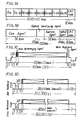
- a standard format is shown in Figure 1.
- Figure 1A illustrates a data block which is to be inserted into one horizontal interval (1 H) and Figure 1B illustrates a control block which is to be inserted into the prior horizontal interval 1 H.
- Audio signals of two channels are respectively sampled at a sampling frequency fs of 44.056 kHz and are converted to data words Ai and Bi each comprising fourteen bits.
- One block comprises a PCM word of six words, two parity words Pi and Qi for error correction, and a cyclic redundancy check (CRC) code of sixteen bits to detect the absence or presence of the aforesaid data having a total of eight words. Accordingly, the length of one block becomes 128 bits.
- CRC cyclic redundancy check
- the parity words Pi and Qi for error correction are formed with respect to the six PCM words and is interleaved word by word.
- suffixes attached to each word show the interleaving relationship where a unit delay is represented by D (one block).
- the control block seen in Figure 1B comprises a cue signal of fifty-six bits, a content identifying signal of fourteen bits, an address signal of twenty-eight bits, a control signal of fourteen bits and a CRC code of sixteen bits so as to detect errors.
- the horizontal synchronizing signal HD is inserted into 1 H (168 bits) of the horizontal synchronizing signal HD.
- a data synchronizing signal is added to the beginning thereof and a white reference signal is added to the end thereof.
- the data interval is 245 H in one field (1 V) excluding an equalizing pulse interval and a vertical synchronizing signal (VD) interval having a total of 9 H (9.5 H for an even-numbered field) and an interval of 7.5 H (7 H for an even-numbered field) to include the head switching timing.
- VD vertical synchronizing signal
- the control block is inserted into the first 1 H.
- FIG. 2 shows an embodiment including a recording encoder and a reproducing decoder.
- each input terminal la and 1b separate analog output signals of the A and B channels derived from a sample-and-hold circuit (not shown) which is supplied through a multiplexer 2 to an analog-to-digital (A/D) converter 3 where they are digitized with one word for each sample.
- the output of the A/D converter 3 is supplied to a serial-parallel converter 4 and is converted to a six parallel words. These six words such as A , B n , A n+1 , B n+1 , A n+2 and B n+2 are supplied to a parity generating circuit 5 and to an interleaving delay circuit 6.
- the parity generating circuit 5 operates as follows: thereby producing first and second parity words.
- reference letter n denotes a multiple of either zero or three
- ⁇ represents a modulo-two addition of each bit corresponding to each word
- T represents a generating matrix.
- the first and second parity words can correct one word error within one block and if the position of the error word is known, two-word errors can also be corrected.
- the interleaving delay circuit 6 is provided to delay the six PCM data series from the serial-parallel converter 4 and the two parity data series from the parity generating circuit 5 by different amounts differing by a unit delay time D (0, D, 2 D, 3 D, 4 D, 5 D, 6 D, 7 D).
- a random access memory is utilized for such delay.
- the write and read addresses of the RAM are controlled so as to perform the interleaving and the frequency of the read clock signal is raised so it is higher than the write clock signal, so that the time-base is compressed thereby forming a data blank corresponding to a vertical blanking period.
- An output of the delay circuit 6 is supplied to a parallel-serial converter 7 and converted to bit serial form, and the CRC code is added to it by a CRC code generator 8 and a switch 9 so as to produce a data output having the form shown in Figure 1A.
- a synchronizing mixing circuit 10 so as to form a recording signal having the same signal format as the television signal shown in Figures 1C and 1D.
- This signal is supplied to a video input terminal of a VTR 11 and to one input terminal 13a of a switch 12.
- a reproduced signal obtained at the video output terminal of the VTR 11 is supplied to another input terminal 13b of the switch 12.
- a signal produced at an output terminal 13c of the switch 12 is supplied to a waveform shaping and data extracting circuit 14 of the reproducing decoder.
- a synchronizing signal is separated from the reproduced signal and is utilized to form a timing pulse signal which is required for data processing by the reproducing system.
- the reproduced data from the circuit 14 is supplied to a series-parallel converter 15 and to an error detecting ciruit 16.
- the error detecting circuit 16 is provided to detect errors by utilizing the CRC code for each block of the reproduced data and produces an error indicator EP which is "1" if an error exists and "0" if no error exists.
- the de-interleaving delay circuit 17 receives the error indicator signal EP as well as the data, and the error indicator signal EP of one bit is added to each word of the data.
- the de-interleaving delay circuit 17 comprises a memory in which addresses are controlled so as to add a predetermined delay, and the frequency of the read clock signal is made lower than the frequency of the write clock signal so as to perform time-base extension.
- Data A n , B n , A n+1' B n+1' A n+2' B n+2' P n and Q n de-interleaved by the delay circuit 17 together with the error indicator signals are supplied to a syndrome generating and abnormality detecting circuit 18 and are also supplied, through a one-block delay circuit 19, to a correcting circuit 20.
- the correcting circuit 20 receives the syndrome signals which have been generated. An uncorrectable erroneous word is interpolated from the mean value in a compensating circuit 21 which is connected to the correcting circuit 20.
- Error indicator signals Pep and Qep relative to two parity data are supplied to an AND gate 22 and the output of the AND gate 22 and an abnormality detected signal from the syndrome generating and abnormality detecting circuit 18 are supplied to an OR gate 23.
- the output of the OR gate 23 is supplied to a flip-flop 24 as the set input (S) and a normal detected signal from the syndrome generating and abnormality detecting circuit 18 is supplied to the flip-flop 24 at the reset input (R).
- correction or compensation of an erroneous word is accomplished as follows.
- Six words W 1 to W 6 and the parity words P and Q are reproduced by an operation as follows: where reference letters Pe and Qe designate error patterns of the parity words P and Q, the error patterns in which, for example, the presence or absence of the error of each bit is respectively represented by "1" or "0", and Wne represents an error pattern of the PCM word.
- the correcting circuit 20 performs the error corrections described above. In cases other than the above, the words identified as erroneous by the error indicator EP are compensated by the compensating circuit 21. However, as is the case described below, if the error position cannot be detected even when the presence of the error is known, the error is detected as an abnormality and an abnormality detecting output is produced so as to inhibit the correction operation and instead, to perform a compensation operation.
- the flip-flop 24 is reset and the flag signal FLG will be "0" so as to discontinue inhibiting of the error correction circuit 20. Absence of an error word can be detected due to the fact that the two syndromes S 1 and S 2 are both represented by "0".
- the flag signal will be "0" according to such detection.
- the embodiment can prevent erroneous corrections in the intervals (4) and (6) from occurring.
- the embodiment since the flag has already been displayed before the error indicators of all the parity words identify the erroneous words, the erroneous correction can be prevented positively and reliably.
Landscapes
- Engineering & Computer Science (AREA)
- Multimedia (AREA)
- Signal Processing (AREA)
- Error Detection And Correction (AREA)
- Transmission Systems Not Characterized By The Medium Used For Transmission (AREA)
Abstract
Description
- This invention relates to pulse code modulated (PCM) signal processing apparatus. Such apparatus is particularly, but not exclusively, suitable for use where an audio signal is digitized for use in a video tape recorder (VTR) or a digital audio disc, so as to reproduce a recorded signal which has been interleaved utilizing an error correction method.
- There has been proposed a PCM signal recording and reproducing apparatus for modulating an analog audio signal such as music to form a PCM signal. An error correction code and an error detection code are added and the signal is converted to a signal format similar to a television signal, for recording and reproduction by a video tape recorder (VTR). In the VTR, when drop-out is caused, for example, by dust on the magnetic tape forming the recording medium, there is a possibility that a burst error will occur in the reproduced PCM signal. If such a burst error occurs, it becomes quite difficult to error-correct the lost data.
- To deal with this problem the following operation is performed. In a PCM processor wherein an audio PCM signal is converted to a quasi-video signal, upon converting the audio PCM signal to the quasi-video signal, that is, during recording, the sample words forming the PCM data are separated into blocks each comprising a predetermined number of words, and an error correction code is generated for each block of PCM data. The PCM data and the error correction code are respectively interleaved so as to have different delay times from each other and the error detection code is further added to the interleaved data. The signals are then converted to a quasi-video signal. When the VTR reproduces the signal thus recorded, the quasi-video signal is converted to the audio PCM signal in an operation which is the opposite of that described above, and de-interleaving is performed so as to disperse the burst error and to correct the data. With such an arrangement, during normal reproduction, all the correction capabilities are utilized so that nearly all of the original PCM data can be reproduced.
- However, when a recording VTR has not as yet been switched to the recording mode and the video signal input terminal of the VTR is directly and electrically connected to a video signal output terminal, and since it is necessary to monitor the input signal thereof even when the VTR is not operating, a mode which is sometimes designated the E-E mode is utilized. In this mode, the video signal output of the PCM processor is directly coupled to the video signal input terminal. When this mode is changed and the VTR is switched to the reproducing mode, or an edited magnetic tape is reproduced, two different mixed data may exist before and after the stage where they are de-interleaved and converted to the correct forms. In such a case, the error correcting circuit may decide that there is an error and perform error correction even although no error in fact exists. The error correcting circuit may therefore produce data which are quite different from the original data, and when such data are supplied to a digital-to- analog (D/A) converter and converted to an audio signal, the audio signal will result in an abnormal sound and may even damage loudspeakers which are coupled to reproduce the audio signal.
- In order to prevent erroneous correction, a method has been proposed where the error decision is made by employing error detection results both from using an error detection code and syndromes formed from the error correction code and the reproduced PCM data. That is, when an error syndrome indicates the presence of an error, although the absence of an error is indicated by error detecting means, and when the syndrome indicates the existence of another erroneous word in addition to the erroneous word identified by the error indicator which is the result of the error detection, and the position thereof is unknown, the error correction is inhibited and instead, all the PCM words within the block are compensated (that is concealed). For compensation, a front-end hold is used to replace the erroneous word with the correct word occuring prior thereto or a mean value interpolation is used to replace the erroneous word with the mean value of the correct words before and after it.
- In these methods, when a burst error occurs at a connection point of the input data, such methods will only be effective if the burst error is short. If the burst error is long there will be many erroneous words in the data after de-interleaving and it becomes impossible to check whether or not the error indicator and the syndrome have a normal relationship, and correction of the errors cannot be made.
- According to the present invention there is provided apparatus for correcting a PCM signal comprising time interleaved binary data words and error correction and error detection words, the apparatus comprising:
- an error detecting circuit receiving the incoming PCM signal;
- a time de-interleaver receiving the incoming signal and separating it into- a plurality of parallel binary data and error correction and error detection words;
- a syndrome generating and abnormality detecting circuit receiving the output of said time de-interleaver;
- a data correcting circuit receiving inputs from said de-interleaver and said syndrome generating and abnormality detecting circuit; and
- an error compensating circuit receiving an output of said data correcting circuit.
- According to the present invention there is also provided a PCM signal processing apparatus arranged to receive successive transmission blocks, each comprising time-interleaved PCM data, and error correction and error detection words, said apparatus comprising:
- detecting means responsive to said error detection words for detecting if a received transmission block contains an error;
- error identifying means for identifying as being erroneous each of the time-interleaved words included in the received transmission block which has been detected as containing an error;
- de-interleaving means for time de-interleaving each received transmission block to recover a de-interleaved block formed of de-interleaved PCM and error-correction words with erroneous de-interleaved words being respectively identified;
- syndrome generating means coupled to said de-interleaving means for generating error syndrome signals using said de-interleaved PCM and said error-correction words in the de-interleaved block;
- error correcting means responsive to said error syndrome for correcting an erroneous PCM word in said de-interleaved block as a function of the remaining non-erroneous PCM and error-correction words in that de-interleaved block;
- error compensating means responsive to the identification of said error identifying means for compensating for said erroneous PCM word in said de-interleaved block with a substitute PCM word when error correction by said error correcting means is not possible; and
- inhibit means which inhibits said error correcting means when all of said error detection words in said de-interleaved block are identified as erroneous and which does not inhibit when the relationship between said error identifying means and said error syndrome signal indicates that no errors exist.
- The invention will now be described by way of example with reference to the accompanying drawings, throughout which like references designate like elements, and in which:
- Figures 1A, 1B, 1C and ID are diagrams showing the format of one block of data and waveforms of the recording signal of an embodiment of the invention;
- Figure 2 is a block diagram showing an arrangement of a recording encoder and a reproducing decoder in an embodiment of the invention; and
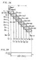
- Figure 3 is a diagram for explaining the operation of an embodiment of the invention.
- An embodiment of the invention comprises an audio PCM signal recording and reproducing apparatus in which a conventional home rotary two-head type VTR is used, and which is not modified but has an adaptor connected to it. Such a PCM signal adaptor converts audio PCM data to a signal format similar to a television signal format. A standard format is shown in Figure 1.
- Figure 1A illustrates a data block which is to be inserted into one horizontal interval (1 H) and Figure 1B illustrates a control block which is to be inserted into the prior
horizontal interval 1 H. Audio signals of two channels are respectively sampled at a sampling frequency fs of 44.056 kHz and are converted to data words Ai and Bi each comprising fourteen bits. One block comprises a PCM word of six words, two parity words Pi and Qi for error correction, and a cyclic redundancy check (CRC) code of sixteen bits to detect the absence or presence of the aforesaid data having a total of eight words. Accordingly, the length of one block becomes 128 bits. The parity words Pi and Qi for error correction are formed with respect to the six PCM words and is interleaved word by word. In Figure 1A, suffixes attached to each word show the interleaving relationship where a unit delay is represented by D (one block). The control block seen in Figure 1B comprises a cue signal of fifty-six bits, a content identifying signal of fourteen bits, an address signal of twenty-eight bits, a control signal of fourteen bits and a CRC code of sixteen bits so as to detect errors. - As illustrated in Figure 1C, into 1 H (168 bits) of the horizontal synchronizing signal HD is inserted one block of 128 bits. A data synchronizing signal is added to the beginning thereof and a white reference signal is added to the end thereof. Also, as illustrated in Figure ID, the data interval is 245 H in one field (1 V) excluding an equalizing pulse interval and a vertical synchronizing signal (VD) interval having a total of 9 H (9.5 H for an even-numbered field) and an interval of 7.5 H (7 H for an even-numbered field) to include the head switching timing. As shown by the cross-hatched section in the figure, the control block is inserted into the first 1 H.
- Figure 2 shows an embodiment including a recording encoder and a reproducing decoder. each input terminal la and 1b separate analog output signals of the A and B channels derived from a sample-and-hold circuit (not shown) which is supplied through a
multiplexer 2 to an analog-to-digital (A/D) converter 3 where they are digitized with one word for each sample. The output of the A/D converter 3 is supplied to a serial-parallel converter 4 and is converted to a six parallel words. These six words such as A , Bn, An+1, Bn+1, An+2 and Bn+2 are supplied to aparity generating circuit 5 and to an interleavingdelay circuit 6. Theparity generating circuit 5 operates as follows:

delay circuit 6 is provided to delay the six PCM data series from the serial-parallel converter 4 and the two parity data series from theparity generating circuit 5 by different amounts differing by a unit delay time D (0, D, 2 D, 3 D, 4 D, 5 D, 6 D, 7 D). In practice, a random access memory (RAM) is utilized for such delay. Thus, the write and read addresses of the RAM are controlled so as to perform the interleaving and the frequency of the read clock signal is raised so it is higher than the write clock signal, so that the time-base is compressed thereby forming a data blank corresponding to a vertical blanking period. An output of thedelay circuit 6 is supplied to a parallel-serial converter 7 and converted to bit serial form, and the CRC code is added to it by aCRC code generator 8 and a switch 9 so as to produce a data output having the form shown in Figure 1A. To this data output are added the synchronizing signal, the equalizing pulse and so forth by a synchronizingmixing circuit 10 so as to form a recording signal having the same signal format as the television signal shown in Figures 1C and 1D. This signal is supplied to a video input terminal of aVTR 11 and to one input terminal 13a of a switch 12. - A reproduced signal obtained at the video output terminal of the
VTR 11 is supplied to another input terminal 13b of the switch 12. A signal produced at an output terminal 13c of the switch 12 is supplied to a waveform shaping anddata extracting circuit 14 of the reproducing decoder. Although not shown, a synchronizing signal is separated from the reproduced signal and is utilized to form a timing pulse signal which is required for data processing by the reproducing system. The reproduced data from thecircuit 14 is supplied to a series-parallel converter 15 and to anerror detecting ciruit 16. Theerror detecting circuit 16 is provided to detect errors by utilizing the CRC code for each block of the reproduced data and produces an error indicator EP which is "1" if an error exists and "0" if no error exists. Eight words appearing at the output of the serial-parallel converter 15, such as An+21D, Bn+18D, An+1+15D, Bn+1+12D, An+2+9D, Bn+2+6D' Pn+3D and Q , are supplied to ade-interleaving delay circuit 17 in which a delay (7 D, 6 D, 5 D, 4 D, 3 D, 2 D, D, 0) is applied so as to cancel the delay caused by the interleaving. In this case, thede-interleaving delay circuit 17 receives the error indicator signal EP as well as the data, and the error indicator signal EP of one bit is added to each word of the data. - In practice, the
de-interleaving delay circuit 17 comprises a memory in which addresses are controlled so as to add a predetermined delay, and the frequency of the read clock signal is made lower than the frequency of the write clock signal so as to perform time-base extension. Data An, Bn, An+1' Bn+1' An+2' Bn+2' Pn and Q n de-interleaved by thedelay circuit 17 together with the error indicator signals are supplied to a syndrome generating andabnormality detecting circuit 18 and are also supplied, through a one-block delay circuit 19, to a correcting circuit 20. The correcting circuit 20 receives the syndrome signals which have been generated. An uncorrectable erroneous word is interpolated from the mean value in a compensating circuit 21 which is connected to the correcting circuit 20. - Error indicator signals Pep and Qep relative to two parity data are supplied to an AND
gate 22 and the output of the ANDgate 22 and an abnormality detected signal from the syndrome generating andabnormality detecting circuit 18 are supplied to anOR gate 23. The output of theOR gate 23 is supplied to a flip-flop 24 as the set input (S) and a normal detected signal from the syndrome generating andabnormality detecting circuit 18 is supplied to the flip-flop 24 at the reset input (R). A flag signal FLG generated by the flip-flop 24 is supplied to the correcting circuit 20 as a control signal and when the FLG = "1", the correcting circuit 20 is enabled so as to correct an error. - Correction or compensation of an erroneous word is accomplished as follows. For the PCM data of one block to generate the parity words P and Q, six words, W1 to W 6 may be considered. Six words W1 to W 6 and the parity words P and Q are reproduced by an operation as follows:


- 1. For a one word error of the PCM words:
- Can be expressed as:

- (a) If P is correct and the error position i is specified by the error indicator EP, since:

- (b) If P is erroneous but Q is correct and the error position i is specified by the error indicator EP, since:

- (c) If P and Q are correct but the erroneous word of a one word error is unknown, the data words have a one word error and if it is represented by Wi: thus S1 = Wie


- (a) If P is correct and the error position i is specified by the error indicator EP, since:
- Can be expressed as:
- 2. If P and Q are correct but two words (Wi, Wj) of the PCM word are erroneous (where each error pattern is given as Wie and Wje, this can be expressed as follows:


- The correcting circuit 20 performs the error corrections described above. In cases other than the above, the words identified as erroneous by the error indicator EP are compensated by the compensating circuit 21. However, as is the case described below, if the error position cannot be detected even when the presence of the error is known, the error is detected as an abnormality and an abnormality detecting output is produced so as to inhibit the correction operation and instead, to perform a compensation operation.
- 3.(a) For a case wherein both P and Q are correct, but the erroneous word is unknown and also the error position i cannot be detected by the method of 1(c), for example, erroneous words of two words or above, although not specified by the error indicator EP.
- (b) P is correct, but Q is erroneous. Although the error point EP of each word of W1 to W6 does not specify the erroneous word, S1≠0 is established.
- (c) Q is correct, but P is erroneous. Although the error pointer EP of each word of WI to W6 does not specify the erroneous word, S2≠0 is established.
- A further description of the embodiment for the case where the switch 12 associated with
VTR 11 is switched from the E-E mode where the input terminal 13a is connected to the output terminal 13c, to the reproducing mode where the input terminal 13b is connected to the output terminal 13c. In a memory area of thede-interleaving delay circuit 17, the reproduced data of one block are sequentially written word by word in each address spaced from each by D = 16 blocks and with respect to the address of the same block, such data are sequentially read out word by word. As shown in Figure 3A, when data (An+21D) (Bn+18D), ...... (Pn+3D) and Qn of a first block of the reproduced data just after the connection point X are written in, together with (Q ), then Q and the reproduced data A , B , ...... P are read out. In this case, if a time beyond 21D after the data is switched is represented by d, for example, it is assumed that a burst error due to drop-out occurs for a period of 35 blocks. If so arranged, all write data, shown by a cross-hatched area in the figure, included in the interval of 35 H after the connection point X, will be in error. If no error exists excluding the above-mentioned error, since the error is a one-word error of the parity word Q during the interval t0 to t1, the reproduced data will be produced as it is. If the timing becomes t1, the error indicators Pep and Qep for the parity word de-interleaved become "1" simultaneously so that the output of the ANDgate 22 will be "1" which will set the flip-flop 24 which will produce the flag signal FLG "1" as shown in Figure 3B. By such a process, the error correcting circuit 20 is inhibited from correcting the error and instead, it will compensate the erroneous word in the PCM word. In this embodiment, during the timing t15 wherein no erroneous word is presented, the flip-flop 24 is reset and the flag signal FLG will be "0" so as to discontinue inhibiting of the error correction circuit 20. Absence of an error word can be detected due to the fact that the two syndromes S1 and S2 are both represented by "0". On the other hand, to detect the normal state during the timing t14 wherein a position of the erroneous word which has been searched from the syndromes S1 and S2 by the method 1(c) described above is made coincident with a position of one word error specified by the error indicator, and the flag signal will be "0" according to such detection. - If the flag signal FLG does not occur thereby not to inhibit the correction operation, the correction or the compensation of the error will be performed as described below.
- (1) Interval to to tl: Since the error is a one word error of the parity word Q, the PCM word is produced as it is.
- (2) Interval t to t2: Since the error is a two word error of the parity data P and Q, the PCM word is produced as it is.
- (3) Interval t2 to t3: Since the error is a total of three word errors of the parity words P and Q and one word of the PCM word, it becomes impossible to correct the errors and hence, the erroneous word of the PCM word is compensated.
- (4) Interval t3 to t4: Since the error is a total of two word errors of the parity word P and one word of the PCM word and the parity word Q is correct, the correction is performed according to the method of l(b) previously described. However, due to correction employing different data, such correction will be erroneous.
- (5) Interval t4 to t5: Since the error is in three words, two erroneous words of the PCM word are compensated.
- (6) Intervals t5 to t6, t7 to t8, t9 to t10 and t11 to t12: Since the parity words P and Q are correct and the error is a two word error of the PCM word, the correction is performed according to the above-mentioned
method 2. However, due to the employment of different data, the correction will be erroneous. - (7) Intervals t6 to t7, t8 to t9, t10 to t11 and t 12 to t 13 : Since the error is a three-word error, each erroneous word is compensated.
- (8) Interval t13 to t14: Since the parity words P and Q are correct and the error is a two-word error of the PCM word, the correction is performed according to the above described
method 2. In this case, since data to be employed are all included in the reproduced data, the correction will correct the errors. - (9) Interval t14 to t15: Since the error is a one word error, the correction is carried out in accordance with the above-described method 1(a). The correction will correct the data.
- The embodiment can prevent erroneous corrections in the intervals (4) and (6) from occurring. Merely by detecting the abnormal relationship between the error indicator and the syndrome, in other words, detecting that the syndrome is not indicated by 0, although the erroneous word is not identified by the error indicator EP, since S1 = 0 and S2 = 0 are established as described above, it is not possible to prevent the erroneous correction from occurring in the interval where the erroneous word is identified by the error indicator EP. However, with the embodiment, since the flag has already been displayed before the error indicators of all the parity words identify the erroneous words, the erroneous correction can be prevented positively and reliably. Moreover, when a burst error having a length d with the relationship D is less than d is less than 2D occurs after the connection point of the different data, the embodiment provides an effective correction.
Claims (7)
Applications Claiming Priority (2)
| Application Number | Priority Date | Filing Date | Title |
|---|---|---|---|
| JP169410/80 | 1980-12-01 | ||
| JP55169410A JPS5794911A (en) | 1980-12-01 | 1980-12-01 | Pcm signal processor |
Publications (3)
| Publication Number | Publication Date |
|---|---|
| EP0053505A2 true EP0053505A2 (en) | 1982-06-09 |
| EP0053505A3 EP0053505A3 (en) | 1983-07-06 |
| EP0053505B1 EP0053505B1 (en) | 1986-12-10 |
Family
ID=15886076
Family Applications (1)
| Application Number | Title | Priority Date | Filing Date |
|---|---|---|---|
| EP81305641A Expired EP0053505B1 (en) | 1980-12-01 | 1981-11-27 | Pulse code modulated signal processing apparatus |
Country Status (6)
| Country | Link |
|---|---|
| US (1) | US4451920A (en) |
| EP (1) | EP0053505B1 (en) |
| JP (1) | JPS5794911A (en) |
| AU (1) | AU542262B2 (en) |
| CA (1) | CA1186765A (en) |
| DE (1) | DE3175714D1 (en) |
Cited By (4)
| Publication number | Priority date | Publication date | Assignee | Title |
|---|---|---|---|---|
| GB2140593A (en) * | 1983-04-30 | 1984-11-28 | Sony Corp | Encoding methods for error correction |
| EP0150811A2 (en) * | 1984-01-25 | 1985-08-07 | Hitachi, Ltd. | Method and apparatus for recording digital signals |
| EP0180764A2 (en) * | 1984-10-05 | 1986-05-14 | Hitachi, Ltd. | Method and apparatus for processing an error flag of a PCM signal |
| EP0790710A3 (en) * | 1995-12-22 | 1997-09-17 | ANSALDO TRASPORTI S.p.A. | Method for rapid validation and coding of cyclic codes |
Families Citing this family (11)
| Publication number | Priority date | Publication date | Assignee | Title |
|---|---|---|---|---|
| US4541091A (en) * | 1982-06-11 | 1985-09-10 | Hitachi, Ltd. | Code error detection and correction method and apparatus |
| GB2124449B (en) * | 1982-07-16 | 1986-11-19 | British Broadcasting Corp | Concealment of defects in a video signal |
| GB2126760B (en) * | 1982-08-20 | 1985-08-29 | Sony Corp | Error correction of digital television signals |
| JPH084233B2 (en) * | 1984-06-29 | 1996-01-17 | 株式会社日立製作所 | Error correction code decoding device |
| JPH07111815B2 (en) * | 1984-07-23 | 1995-11-29 | 株式会社日立製作所 | Digital signal recording system |
| NL8402411A (en) * | 1984-08-02 | 1986-03-03 | Philips Nv | DEVICE FOR CORRECTING AND MASKING ERRORS IN AN INFORMATION FLOW, AND DISPLAY FOR DISPLAYING IMAGES AND / OR SOUND PROVIDED WITH SUCH A DEVICE. |
| US4792953A (en) * | 1986-03-28 | 1988-12-20 | Ampex Corporation | Digital signal error concealment |
| JPH0549532U (en) * | 1991-12-10 | 1993-06-29 | 住友電装株式会社 | Rear wiper drive for vehicle |
| US5745505A (en) * | 1994-03-01 | 1998-04-28 | Sony Corporation | Digital signal encoding method and apparatus, digital signal recording medium, and digital signal decoding method and apparatus |
| US5577054A (en) * | 1994-09-13 | 1996-11-19 | Philips Electronics North America Corporation | Device and method for performing error detection on an interleaved signal portion, and a receiver and decoding method employing such error detection |
| US6047036A (en) * | 1997-05-02 | 2000-04-04 | Advanced Micro Devices, Inc. | System and method for implementing a mute voice signal upon reception of a ADPCM zero nibble in wireless communications |
Citations (4)
| Publication number | Priority date | Publication date | Assignee | Title |
|---|---|---|---|---|
| GB2019168A (en) * | 1978-04-17 | 1979-10-24 | Sony Corp | Error correcting system |
| FR2440593A1 (en) * | 1978-11-03 | 1980-05-30 | Ampex | METHOD AND APPARATUS USING AN IMPROVED FORMAT FOR RECORDING AND REPRODUCING DIGITAL ACOUSTIC DATA |
| US4234896A (en) * | 1978-11-13 | 1980-11-18 | Mitsubishi Denki Kabushiki Kaisha | PCM Recording and reproducing system |
| GB2071370A (en) * | 1980-01-24 | 1981-09-16 | Sony Corp | PCM Signal Processing |
Family Cites Families (4)
| Publication number | Priority date | Publication date | Assignee | Title |
|---|---|---|---|---|
| JPS5380105A (en) * | 1976-12-24 | 1978-07-15 | Sony Corp | Digital signal transmission method |
| JPS5556744A (en) * | 1978-10-23 | 1980-04-25 | Sony Corp | Pcm signal transmission device |
| JPS5657374A (en) * | 1979-10-16 | 1981-05-19 | Sony Corp | Processor of digital video signal |
| US4380071A (en) * | 1981-02-02 | 1983-04-12 | Sony Corporation | Method and apparatus for preventing errors in PCM signal processing apparatus |
-
1980
- 1980-12-01 JP JP55169410A patent/JPS5794911A/en active Granted
-
1981
- 1981-11-23 CA CA000390687A patent/CA1186765A/en not_active Expired
- 1981-11-24 AU AU77813/81A patent/AU542262B2/en not_active Ceased
- 1981-11-25 US US06/324,816 patent/US4451920A/en not_active Expired - Fee Related
- 1981-11-27 EP EP81305641A patent/EP0053505B1/en not_active Expired
- 1981-11-27 DE DE8181305641T patent/DE3175714D1/en not_active Expired
Patent Citations (4)
| Publication number | Priority date | Publication date | Assignee | Title |
|---|---|---|---|---|
| GB2019168A (en) * | 1978-04-17 | 1979-10-24 | Sony Corp | Error correcting system |
| FR2440593A1 (en) * | 1978-11-03 | 1980-05-30 | Ampex | METHOD AND APPARATUS USING AN IMPROVED FORMAT FOR RECORDING AND REPRODUCING DIGITAL ACOUSTIC DATA |
| US4234896A (en) * | 1978-11-13 | 1980-11-18 | Mitsubishi Denki Kabushiki Kaisha | PCM Recording and reproducing system |
| GB2071370A (en) * | 1980-01-24 | 1981-09-16 | Sony Corp | PCM Signal Processing |
Cited By (8)
| Publication number | Priority date | Publication date | Assignee | Title |
|---|---|---|---|---|
| GB2140593A (en) * | 1983-04-30 | 1984-11-28 | Sony Corp | Encoding methods for error correction |
| US4630272A (en) * | 1983-04-30 | 1986-12-16 | Sony Corporation | Encoding method for error correction |
| AU575822B2 (en) * | 1983-04-30 | 1988-08-11 | Sony Corporation | Encoding method for error correction |
| EP0150811A2 (en) * | 1984-01-25 | 1985-08-07 | Hitachi, Ltd. | Method and apparatus for recording digital signals |
| EP0150811A3 (en) * | 1984-01-25 | 1987-08-05 | Hitachi, Ltd. | Method and apparatus for recording digital signals |
| EP0180764A2 (en) * | 1984-10-05 | 1986-05-14 | Hitachi, Ltd. | Method and apparatus for processing an error flag of a PCM signal |
| EP0180764A3 (en) * | 1984-10-05 | 1988-08-10 | Hitachi, Ltd. | Method and apparatus for processing an error flag of a pcm signal |
| EP0790710A3 (en) * | 1995-12-22 | 1997-09-17 | ANSALDO TRASPORTI S.p.A. | Method for rapid validation and coding of cyclic codes |
Also Published As
| Publication number | Publication date |
|---|---|
| US4451920A (en) | 1984-05-29 |
| CA1186765A (en) | 1985-05-07 |
| AU7781381A (en) | 1982-06-10 |
| JPH0221077B2 (en) | 1990-05-11 |
| DE3175714D1 (en) | 1987-01-22 |
| EP0053505A3 (en) | 1983-07-06 |
| AU542262B2 (en) | 1985-02-14 |
| JPS5794911A (en) | 1982-06-12 |
| EP0053505B1 (en) | 1986-12-10 |
Similar Documents
| Publication | Publication Date | Title |
|---|---|---|
| US4882732A (en) | Method and apparatus for recording and/or reproducing digital data | |
| US4211997A (en) | Method and apparatus employing an improved format for recording and reproducing digital audio | |
| US4238852A (en) | Error correcting system | |
| US4145683A (en) | Single track audio-digital recorder and circuit for use therein having error correction | |
| EP0048151B1 (en) | A pcm signal processor | |
| US4622600A (en) | Rotary-head type PCM data recording/reproducing method and apparatus with a redundancy-reduced control data format | |
| EP0029226B1 (en) | System for processing audio pcm digital signals | |
| EP0053505B1 (en) | Pulse code modulated signal processing apparatus | |
| US4188616A (en) | Method and system for transmitting and receiving blocks of encoded data words to minimize error distortion in the recovery of said data words | |
| EP0098082B1 (en) | Methods of and apparatus for digital audio signal processing | |
| US4748628A (en) | Method and apparatus for correcting errors in digital audio signals | |
| JPH0345476B2 (en) | ||
| EP0048933B1 (en) | Circuit for correcting error in digital information signal | |
| GB2037036A (en) | Format for digital tape recorder | |
| KR0139413B1 (en) | Encoding apparatus and method for error correction | |
| US4451919A (en) | Digital signal processor for use in recording and/or reproducing equipment | |
| EP0048150B1 (en) | A pcm signal processor | |
| US4445216A (en) | System for defeating erroneous correction in a digital signal reproducing apparatus | |
| EP0053474B1 (en) | Pulse code modulated signal processing apparatus | |
| EP0395125A2 (en) | A PCM recording and reproducing apparatus | |
| JPS6333748B2 (en) | ||
| US4853798A (en) | Method and apparatus for reproducing digital or analog signals | |
| JPS6117060B2 (en) | ||
| JP3066046B2 (en) | Video tape recorder | |
| KR830000671B1 (en) | Single-track digital recorder with error correction circuit |
Legal Events
| Date | Code | Title | Description |
|---|---|---|---|
| PUAI | Public reference made under article 153(3) epc to a published international application that has entered the european phase |
Free format text: ORIGINAL CODE: 0009012 |
|
| AK | Designated contracting states |
Designated state(s): DE FR GB IT NL |
|
| PUAL | Search report despatched |
Free format text: ORIGINAL CODE: 0009013 |
|
| AK | Designated contracting states |
Designated state(s): DE FR GB IT NL |
|
| 17P | Request for examination filed |
Effective date: 19831125 |
|
| RAP1 | Party data changed (applicant data changed or rights of an application transferred) |
Owner name: SONY CORPORATION Owner name: KABUSHIKI KAISHA TOSHIBA |
|
| GRAA | (expected) grant |
Free format text: ORIGINAL CODE: 0009210 |
|
| AK | Designated contracting states |
Kind code of ref document: B1 Designated state(s): DE FR GB IT NL |
|
| ET | Fr: translation filed | ||
| REF | Corresponds to: |
Ref document number: 3175714 Country of ref document: DE Date of ref document: 19870122 |
|
| ITF | It: translation for a ep patent filed |
Owner name: SOCIETA' ITALIANA BREVETTI S.P.A. |
|
| PLBE | No opposition filed within time limit |
Free format text: ORIGINAL CODE: 0009261 |
|
| STAA | Information on the status of an ep patent application or granted ep patent |
Free format text: STATUS: NO OPPOSITION FILED WITHIN TIME LIMIT |
|
| 26N | No opposition filed | ||
| ITTA | It: last paid annual fee | ||
| PGFP | Annual fee paid to national office [announced via postgrant information from national office to epo] |
Ref country code: GB Payment date: 19941125 Year of fee payment: 14 |
|
| PGFP | Annual fee paid to national office [announced via postgrant information from national office to epo] |
Ref country code: FR Payment date: 19941129 Year of fee payment: 14 |
|
| PGFP | Annual fee paid to national office [announced via postgrant information from national office to epo] |
Ref country code: NL Payment date: 19941130 Year of fee payment: 14 |
|
| PGFP | Annual fee paid to national office [announced via postgrant information from national office to epo] |
Ref country code: DE Payment date: 19950130 Year of fee payment: 14 |
|
| PG25 | Lapsed in a contracting state [announced via postgrant information from national office to epo] |
Ref country code: GB Effective date: 19951127 |
|
| PG25 | Lapsed in a contracting state [announced via postgrant information from national office to epo] |
Ref country code: NL Effective date: 19960601 |
|
| GBPC | Gb: european patent ceased through non-payment of renewal fee |
Effective date: 19951127 |
|
| PG25 | Lapsed in a contracting state [announced via postgrant information from national office to epo] |
Ref country code: FR Effective date: 19960731 |
|
| NLV4 | Nl: lapsed or anulled due to non-payment of the annual fee |
Effective date: 19960601 |
|
| PG25 | Lapsed in a contracting state [announced via postgrant information from national office to epo] |
Ref country code: DE Effective date: 19960801 |
|
| REG | Reference to a national code |
Ref country code: FR Ref legal event code: ST |