EP0033337B1 - Digital loop synchronization circuit - Google Patents
Digital loop synchronization circuit Download PDFInfo
- Publication number
- EP0033337B1 EP0033337B1 EP80901606A EP80901606A EP0033337B1 EP 0033337 B1 EP0033337 B1 EP 0033337B1 EP 80901606 A EP80901606 A EP 80901606A EP 80901606 A EP80901606 A EP 80901606A EP 0033337 B1 EP0033337 B1 EP 0033337B1
- Authority
- EP
- European Patent Office
- Prior art keywords
- bit
- frame
- loop
- register
- clock
- Prior art date
- Legal status (The legal status is an assumption and is not a legal conclusion. Google has not performed a legal analysis and makes no representation as to the accuracy of the status listed.)
- Expired
Links
Images


Classifications
-
- H—ELECTRICITY
- H04—ELECTRIC COMMUNICATION TECHNIQUE
- H04L—TRANSMISSION OF DIGITAL INFORMATION, e.g. TELEGRAPHIC COMMUNICATION
- H04L12/00—Data switching networks
- H04L12/28—Data switching networks characterised by path configuration, e.g. LAN [Local Area Networks] or WAN [Wide Area Networks]
- H04L12/42—Loop networks
- H04L12/422—Synchronisation for ring networks
-
- H—ELECTRICITY
- H04—ELECTRIC COMMUNICATION TECHNIQUE
- H04J—MULTIPLEX COMMUNICATION
- H04J3/00—Time-division multiplex systems
- H04J3/02—Details
- H04J3/06—Synchronising arrangements
- H04J3/062—Synchronisation of signals having the same nominal but fluctuating bit rates, e.g. using buffers
- H04J3/0626—Synchronisation of signals having the same nominal but fluctuating bit rates, e.g. using buffers plesiochronous multiplexing systems, e.g. plesiochronous digital hierarchy [PDH], jitter attenuators
-
- H—ELECTRICITY
- H04—ELECTRIC COMMUNICATION TECHNIQUE
- H04Q—SELECTING
- H04Q11/00—Selecting arrangements for multiplex systems
- H04Q11/04—Selecting arrangements for multiplex systems for time-division multiplexing
Definitions
- This invention relates to a synchronization circuit for use in a digital communication system having a plurality of serially interconnected stations, the stations arranged for intercommunication via a digital data channel, the channel divided into frames with each frame having a fixed number n positions, said synchronization circuit comprising first and second clock, means for generating a frame synchronization bit and comparing means.
- a synchronization circuit for use in a digital communication system having a plurality of serially interconnected stations, the stations arranged for intercommunication via a digital data channel, the channel divided into frames with each frame having a fixed number n positions, said synchronization circuit comprising first and second clock, means for generating a frame synchronization bit and comparing means.
- the problem is to design a digital loop communication system having the capability of easily adding and subtracting stations from the loop while at the same time maintaining synchronization around the loop regardless of the number of stations in the loop at any given time. Since each station is assigned to a particular bit position in the digital stream it is critical that at the completion of one complete frame a given bit position be presented to the proper station. This is termed loop synchronization and it is clear that as stations are added or subtracted, time delays must be added or subtracted from the loop if synchronization is to be maintained.
- Another method of synchronization uses a dual shift- register technique.
- One bank of registers is used to hold data and another bank of registers contains "marker bits" which control the speed of clocking of the data register. Control circuitry manipulates these marker bits until the system is synchronized.
- This technique operates automatically (without external intervention), however, it requires a relatively large amount of hardware and is fairly slow to detect and correct out-of-sync conditions.
- an improved form of the synchronization circuit in that a synchronizing bit is placed in each frame on the digital data channel, a first in and first out (FIFO) register is provided for insertion in the digital channel between any two of the stations so that the bits of each of the frame as well as the frame synchronizing bit pass from an input to an output of said register, the first clock is effective for controlling the bits into said register one bit at a time, the second clock is effective for controlling bits out of said register one bit at a time, the comparing circuitry is effective for comparing the frame synchronization bit of a particular frame at the output of said register with a generated frame synchronizing bit of a next frame on the digital data channel, and inhibiting apparatus is provided responsive to a mismatch between the compared bits for inhibiting said second clock so as to inhibit the checking of one bit out of said register while still allowing one bit to be clocked into said register by the first clock.
- FIFO first in and first out
- the proposed circuit operates to subtract or add delay as necessary. If the frame bit is not received in the anticipated position the second (output) clock skips one count per frame until the frame bit is received thereby adding delay. If the FIFO register fills up, it is reset and the process continues until the correct synchronizing delay is achieved. The circuit operates for situations where the frame bit is on a separate channel and also when the frame bit is on the actual data channel.
- the loop control module of the present invention is designed for use in a digital loop system. In general, however, it is desired to communicate digital data bits around a closed loop between any number of stations. Stations may be added or removed from the loop from time to time and the loop must compensate for such additions or subtractions. Since the time it takes a particular data bit to traverse the entire loop is dependent upon the number of stations (length) of the loop our invention is directed to the problem of maintaining synchronism of the data bits around a closed digital loop without need for external control.
- LCM 20 loop control module 20 performs four basic functions: generation of clock and frame signals; auto- zeroing on the continuous data bus; garbage collection (removal of undeliverable data) on the bursty data bus; and maintaining the proper loop delay so that the system remains synchronized.
- clock circuit 30 the clock and frame generation are performed by clock circuit 30. These functions may be performed in a standard way using TTL (Transistor-Transistor Logic) integrated circuits.
- TTL Transistor-Transistor Logic
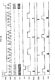
- the timing of the signals generated by the clock circuit is shown in Fig. 8. The function of these signals is as follows:
- the continuous data bus consists of a repetitive sequence of 12 time slots, each consisting of 16 clocks.
- the time slots are used to contain linear PCM voice samples.
- a single continuous data bus can permit up to 12 simultaneous voice conversations.
- the digital voice bus described above has no loss (or attenuation), hence the effects of random bit errors will persist until the system is turned off. Also, the bus tends to contain random bit patterns when it is initially turned on, and these will also persist.
- the circuit of Fig. 5 implements the following algorithm: if the contents of a particular continuous time slot are negative, its value is increased by 1; if the contents of the continuous time slot are positive, its value is decreased by 1; if the value of the continuous time slot is zero, it remains unchanged. Thus, the value of each continuous time time-slot is continuously forced towards zero, and the effect of bit errors is damped out. Since the voice samples are in the form of linear PCM, the addition and subtraction are easily performed. Using 2's complement arithmetic, subtracting 1 is accomplished by adding a sequence of 16 1 's to the continuous time slot.
- serial adder 607 performs the actual addition and subtraction.
- Registers 601 and 602 hold the voice sample to be processed.
- flip-flop 606 latches up the value of bit 15 of the continuous time slot. This bit indicates whether the value of the continuous time slot is positive or negative. If the value of the continuous time slot is positive, the Q output of flip-flop 606 will be high, and a sequence of 16 ones (-1 in 2's complement notation) will be added to the continuous time slot as it is shifted by.
- the output of gate 611 will go high only while BITTMO is asserted (i.e., during the first clock period of the continuous time slot) and a single 1 is added to the least significant bit position of the continuous time slot. If the value of the continuous time slot is identically zero, then the output of gate 612 will be low at the time of the first rising edge of ZTEST. This will cause ZERO signal to be latched at zero and prevent anything from being added to the continuous time slot.
- the circuit of Fig. 5 implements the algorithm described above.
- circuit of Fig. 5 is simply replicated for each additional bus.
- the bursty data bus consists of six bursty time slots each consisting of 32 clocks. While the message-switched timeslots and the call processing field have different functions in the system as far as the LCM is concerned all six of the bursty data bus time slots are identical.
- the function of the bursty data bus circuit (element 50 in Fig. 2) is twofold: 1) to remove traffic from the bursty data bus (i.e., zero out the bursty time slot) after it has been delivered; and 2) to locate and remove any undeliverable traffic.
- the Bursty Data Bus Circuit utilizes three bits of each time slot to carry out these functions: the BUSY/IDLE (B/I), Traffic Control (TC) and Acknowledgement (ACK) bits.
- B/I BUSY/IDLE
- TC Traffic Control
- ACK Acknowledgement
- the relative positions of these bits in a time slot is shown in Fig. 7.
- a programmable data interchanger PDI
- transmits in a time slot it sets the B/I bit to indicate that the time slot is in use.
- the destination PDI receives the time slot, it sets the ACK bit.
- the LCM detects a bursty time slot with both the B/I and ACK bits set, the bursty time-slot is cleared so that it can be used again.
- the Bursty Data Bus Circuit detects a time slot with B/I set, but neither ACK nor TC set, it sets the TC bit to indicate that the bursty time slot has passed by the Bursty Data Bus Circuit once. If a bursty time slot is detected with the B/I and TC bits set, and ACK is not set, this indicates that the bursty time slot has made at least one full trip around the loop without being received and acknowledged. Therefore, it is considered to be undeliverable and the bursty time slot is cleared out.
- the Bursty Data Bus Circuit 50 shown in Fig. 4 performs the above-described functions. Data from the data bus is shifted through flip-flops 501 and 502, registers 503-506, and flip-flops 507 and 508. At the time that DBTEST is asserted (shown in Fig. 8), a complete data time slot is contained between flip-flops 501 and 508. The ACK and TC bits are replicated in flip-flops 509 and 510, respectively, to prevent race conditions. The B/I bit (BUSY) is available at flip-flop 507. The combination of gates 511 through 515 perform the comparisons described above when they are strobed by DBTEST.
- BYTEC When a properly acknowledged time slot is detected, BYTEC is asserted, causing the time slot to be cleared (CLRTS) and also incrementing byte counter 518.
- the byte counter is useful for measuring the traffic handled by the system.
- GARBC When an undeliverable time slot is detected, GARBC is asserted, which causes the time slot to be cleared and increments undeliverable data counter 517.
- the undeliverable data counter is useful for maintaining the system in proper operating condition. A non-zero reading on the undeliverable data counter usually indicates a malfunction somewhere in the system.
- SETTC When a bursty time slot with BUSY asserted, but neither TC nor ACK asserted, is encountered, SETTC is asserted, causing the TC bit to be set.
- the Bursty Data Bus Circuit prevents the data bus from filling up with undeliverable data and keeps statistics relating to the systems performance.
- the number of bits delay around the loop must equal the number of bits per frame (N) if the system is synchronized.
- N the number of bits per frame
- the LCM has a minimum delay of 32 bits, each PDI has a delay of 1 bit, and the frame length is 192 bits. If there are m PDI's in the loop, then the LCM must provide a delay d of: For example, if there are 61 PDI's in the loop, the LCM must provide a delay of 99 bits.
- a FIFO First In-First Out serial memory
- a FIFO is a shift register with separate clocks for the input and output. Bits of data clocked into the FIFO bubble through to the unoccupied storage locations nearest the output. When the FIFO output is clocked, the oldest data bit exits the FIFO and all the other data bits move one slot closer to the output.
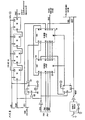
- Figs. 1 and 2 the particular implementation shown uses separate buses for the transmission of continuous data, bursty data, clock, and framing information.
- the frame bus contains only the frame pulse, which occurs every 192 clock periods (Fig. 8).
- the circuit of Fig. 3 uses a FIFO (410 and 411) as an adaptively variable delay which can be used to adjust the loop length.
- the basic principle of operation of the circuit is that, if the system is in sync, the previous frame pulse should emerge from the FIFO at the same time as the new frame pulse is generated.
- FIFO's 410 and 411 are arranged in a standard configuration such that the two 96- word FIFO's become a single 192-word FIFO.
- the FIFO circuit 40 illustrated in Fig. 3 operates in the following manner.
- Flip-flop 405, in conjunction with gate 406 tests the frame bit emerging from the FIFO against the new frame bit being generated. If the system is in sync, the Q output of flip-flop 405 remains high and gate 407 remains enabled. If the system is out of sync, the Q output of flip-flop 405 will go low, disabling gate 407 and interrupting the FIFO's output clock.
- FR+1 is used to set flip-flop 405 and re-enable the FIFO output clock. Thus, one clock has been withheld from the FIFO output, causing the effective loop delay to be lengthened by 1 bit.
- the loop length is increased by one bit per frame until synchronization is achieved. For example, if a station is removed from the loop, the system requires one frame to regain sync.
- the loop length continues to increase by one bit per frame until the FIFO is full.
- the FIFO full condition is detected by flip-flop 412, which clears the FIFO.
- the above synchronization procedures are automatically executed when the system is powered up and every time sync is lost.
- the FIFO circuit adaptively seeks out the correct loop length and automatically maintains it.
- Another extension of this technique is to detect an out-of-sync condition in one frame and add all the required bits of delay in the succeeding frame (rather than adding only one bit of delay per frame). This has the advantage of faster operation at the expense of a small amount of additional hardware.
- a minor modification allows this technique to be used in systems which have a multi-frame delay around the loop. This may be advantageous since it allows more stations to be connected to the loop. If it is desired to maintain a delay of m frames (each frame having N - bits), then a FIFO of capacity mN must be used in conjunction with a frame counter which allows the frame comparison (gate 406) to occur only every m th frame and inhibits it in the intervening frames.
Landscapes
- Engineering & Computer Science (AREA)
- Computer Networks & Wireless Communication (AREA)
- Signal Processing (AREA)
- Computer Hardware Design (AREA)
- Small-Scale Networks (AREA)
- Synchronisation In Digital Transmission Systems (AREA)
- Time-Division Multiplex Systems (AREA)
Abstract
Description
- This invention relates to a synchronization circuit for use in a digital communication system having a plurality of serially interconnected stations, the stations arranged for intercommunication via a digital data channel, the channel divided into frames with each frame having a fixed number n positions, said synchronization circuit comprising first and second clock, means for generating a frame synchronization bit and comparing means. Such a system is disclosed in U.S. 3,681,759.
- In essence, the problem is to design a digital loop communication system having the capability of easily adding and subtracting stations from the loop while at the same time maintaining synchronization around the loop regardless of the number of stations in the loop at any given time. Since each station is assigned to a particular bit position in the digital stream it is critical that at the completion of one complete frame a given bit position be presented to the proper station. This is termed loop synchronization and it is clear that as stations are added or subtracted, time delays must be added or subtracted from the loop if synchronization is to be maintained.
- One method of accomplishing such time padding as disclosed in U.S. 3,732,374, is to use a multi-delay shift register and tap the various outputs depending upon the length of the loop desired. While such a system could work, it has the drawback of requiring external manipulation of the shift register with manually operated switches or with central processing control. In either event, maintaining synchronism becomes an expensive proposition.
- Another method of synchronization, as disclosed in U.S. 3,919,484, uses a dual shift- register technique. One bank of registers is used to hold data and another bank of registers contains "marker bits" which control the speed of clocking of the data register. Control circuitry manipulates these marker bits until the system is synchronized. This technique operates automatically (without external intervention), however, it requires a relatively large amount of hardware and is fairly slow to detect and correct out-of-sync conditions.
- In accordance with the present invention there is provided an improved form of the synchronization circuit as aforesaid, in that a synchronizing bit is placed in each frame on the digital data channel, a first in and first out (FIFO) register is provided for insertion in the digital channel between any two of the stations so that the bits of each of the frame as well as the frame synchronizing bit pass from an input to an output of said register, the first clock is effective for controlling the bits into said register one bit at a time, the second clock is effective for controlling bits out of said register one bit at a time, the comparing circuitry is effective for comparing the frame synchronization bit of a particular frame at the output of said register with a generated frame synchronizing bit of a next frame on the digital data channel, and inhibiting apparatus is provided responsive to a mismatch between the compared bits for inhibiting said second clock so as to inhibit the checking of one bit out of said register while still allowing one bit to be clocked into said register by the first clock.
- As stations are added or subtracted from the loop, the proposed circuit operates to subtract or add delay as necessary. If the frame bit is not received in the anticipated position the second (output) clock skips one count per frame until the frame bit is received thereby adding delay. If the FIFO register fills up, it is reset and the process continues until the correct synchronizing delay is achieved. The circuit operates for situations where the frame bit is on a separate channel and also when the frame bit is on the actual data channel.
- These and other objects, features and problems are solved in one embodiment of our invention, which is described in conjunction with the accompanying drawings, in which:
- Fig. 1 is a block diagram of the entire system;
- Fig. 2 is a block diagram of the loop control module;
- Figs. 3 through 5 are schematic diagrams;
- Fig. 6 illustrates the frame structure of the continuous data bus;
- Fig. 7 illustrates the frame structure of the bursty data bus;
- Fig. 8 is a timing diagram.
- The loop control module of the present invention is designed for use in a digital loop system. In general, however, it is desired to communicate digital data bits around a closed loop between any number of stations. Stations may be added or removed from the loop from time to time and the loop must compensate for such additions or subtractions. Since the time it takes a particular data bit to traverse the entire loop is dependent upon the number of stations (length) of the loop our invention is directed to the problem of maintaining synchronism of the data bits around a closed digital loop without need for external control.
- The following will describe in detail the operation of loop control module (LCM) 20 (Fig. 1
LCM 20 performs four basic functions: generation of clock and frame signals; auto- zeroing on the continuous data bus; garbage collection (removal of undeliverable data) on the bursty data bus; and maintaining the proper loop delay so that the system remains synchronized. - Referring to Fig. 2, the clock and frame generation are performed by
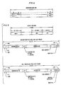
clock circuit 30. These functions may be performed in a standard way using TTL (Transistor-Transistor Logic) integrated circuits. The timing of the signals generated by the clock circuit is shown in Fig. 8. The function of these signals is as follows: - FRAME: marks the beginning of each frame on both the continuous and bursty data buses. Occurs once every 192 CLOCK'S.
- CLOCK: the basic bit clock used throughout the system.
- CLKX2, CLKX4: higher speed versions of CLOCK.
- FR+1: A signal which appears early in each frame-used to set a flip-flop.
- STVTS: marks the start of each time slot on the continuous data bus hereinafter called continuous time slot. Occurs every 16 CLOCKS.
- DBTEST: marks the end of each time slot on the bursty data bus hereinafter called bursty time slot. Occurs every 32 CLOCKS.
- ENDVTS: marks the end of each time slot on the continuous data bus. Occurs every 16 CLOCKS.
- BITTMO: occurs during the first clock period of each continuous data time slot.
- ZTEST: occurs at the end of each time slot on the continuous bus and is used to check if the contents of the time slot has a zero value.
- The use of each of these signals will be explained in the discussions which follow.
- The continuous data bus consists of a repetitive sequence of 12 time slots, each consisting of 16 clocks. In this implementation, the time slots are used to contain linear PCM voice samples. Thus, a single continuous data bus can permit up to 12 simultaneous voice conversations.
- Unlike an analog bus, the digital voice bus described above has no loss (or attenuation), hence the effects of random bit errors will persist until the system is turned off. Also, the bus tends to contain random bit patterns when it is initially turned on, and these will also persist.
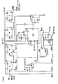
- In order to damp out the effects of bit errors, it is necessary to make the bus slightly lossy (similar to a leaky capacitor in an analog bus). This is done by the
voice circuit 60 in Fig. 2. A schematic of this circuit is given in Fig. 5. When the continuous data bus is used for high-speed data other than linear PCM voice samples, this circuit is omitted. - The circuit of Fig. 5 implements the following algorithm: if the contents of a particular continuous time slot are negative, its value is increased by 1; if the contents of the continuous time slot are positive, its value is decreased by 1; if the value of the continuous time slot is zero, it remains unchanged. Thus, the value of each continuous time time-slot is continuously forced towards zero, and the effect of bit errors is damped out. Since the voice samples are in the form of linear PCM, the addition and subtraction are easily performed. Using 2's complement arithmetic, subtracting 1 is accomplished by adding a sequence of 16 1 's to the continuous time slot.
- With reference to Fig. 5,
serial adder 607 performs the actual addition and subtraction.Registers flop 606 latches up the value ofbit 15 of the continuous time slot. This bit indicates whether the value of the continuous time slot is positive or negative. If the value of the continuous time slot is positive, the Q output of flip-flop 606 will be high, and a sequence of 16 ones (-1 in 2's complement notation) will be added to the continuous time slot as it is shifted by. If, however, the continuous time slot was negative, then the output of gate 611 will go high only while BITTMO is asserted (i.e., during the first clock period of the continuous time slot) and a single 1 is added to the least significant bit position of the continuous time slot. If the value of the continuous time slot is identically zero, then the output ofgate 612 will be low at the time of the first rising edge of ZTEST. This will cause ZERO signal to be latched at zero and prevent anything from being added to the continuous time slot. Thus, the circuit of Fig. 5 implements the algorithm described above. - In systems which have more than one continuous data bus, the circuit of Fig. 5 is simply replicated for each additional bus.
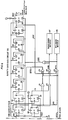
- As shown in Fig. 7, the bursty data bus consists of six bursty time slots each consisting of 32 clocks. While the message-switched timeslots and the call processing field have different functions in the system as far as the LCM is concerned all six of the bursty data bus time slots are identical. The function of the bursty data bus circuit (
element 50 in Fig. 2) is twofold: 1) to remove traffic from the bursty data bus (i.e., zero out the bursty time slot) after it has been delivered; and 2) to locate and remove any undeliverable traffic. - The Bursty Data Bus Circuit (50) utilizes three bits of each time slot to carry out these functions: the BUSY/IDLE (B/I), Traffic Control (TC) and Acknowledgement (ACK) bits. The relative positions of these bits in a time slot is shown in Fig. 7. When a programmable data interchanger (PDI) transmits in a time slot, it sets the B/I bit to indicate that the time slot is in use. When the destination PDI receives the time slot, it sets the ACK bit. When the LCM detects a bursty time slot with both the B/I and ACK bits set, the bursty time-slot is cleared so that it can be used again. If the Bursty Data Bus Circuit detects a time slot with B/I set, but neither ACK nor TC set, it sets the TC bit to indicate that the bursty time slot has passed by the Bursty Data Bus Circuit once. If a bursty time slot is detected with the B/I and TC bits set, and ACK is not set, this indicates that the bursty time slot has made at least one full trip around the loop without being received and acknowledged. Therefore, it is considered to be undeliverable and the bursty time slot is cleared out.
- The Bursty
Data Bus Circuit 50, shown in Fig. 4 performs the above-described functions. Data from the data bus is shifted through flip-flops flops flops flops flop 507. The combination ofgates 511 through 515 perform the comparisons described above when they are strobed by DBTEST. When a properly acknowledged time slot is detected, BYTEC is asserted, causing the time slot to be cleared (CLRTS) and also incrementingbyte counter 518. The byte counter is useful for measuring the traffic handled by the system. When an undeliverable time slot is detected, GARBC is asserted, which causes the time slot to be cleared and increments undeliverable data counter 517. The undeliverable data counter is useful for maintaining the system in proper operating condition. A non-zero reading on the undeliverable data counter usually indicates a malfunction somewhere in the system. When a bursty time slot with BUSY asserted, but neither TC nor ACK asserted, is encountered, SETTC is asserted, causing the TC bit to be set. - In this manner, the Bursty Data Bus Circuit prevents the data bus from filling up with undeliverable data and keeps statistics relating to the systems performance.
- As discussed previously, the number of bits delay around the loop must equal the number of bits per frame (N) if the system is synchronized. In a loop system with N bits per frame, there will not always be exactly N stations connected to the loop. In this particular implementation, the LCM has a minimum delay of 32 bits, each PDI has a delay of 1 bit, and the frame length is 192 bits. If there are m PDI's in the loop, then the LCM must provide a delay d of:

- Since the loop synchronization control circuit is implemented with a FIFO, the operational characteristics of a FIFO will now be briefly described. A FIFO (First In-First Out serial memory) is a shift register with separate clocks for the input and output. Bits of data clocked into the FIFO bubble through to the unoccupied storage locations nearest the output. When the FIFO output is clocked, the oldest data bit exits the FIFO and all the other data bits move one slot closer to the output.
- As illustrated in Figs. 1 and 2, the particular implementation shown uses separate buses for the transmission of continuous data, bursty data, clock, and framing information. The frame bus contains only the frame pulse, which occurs every 192 clock periods (Fig. 8). The circuit of Fig. 3 uses a FIFO (410 and 411) as an adaptively variable delay which can be used to adjust the loop length. The basic principle of operation of the circuit is that, if the system is in sync, the previous frame pulse should emerge from the FIFO at the same time as the new frame pulse is generated. FIFO's 410 and 411 are arranged in a standard configuration such that the two 96- word FIFO's become a single 192-word FIFO.
- The
FIFO circuit 40 illustrated in Fig. 3 operates in the following manner. Flip-flop 405, in conjunction withgate 406 tests the frame bit emerging from the FIFO against the new frame bit being generated. If the system is in sync, the Q output of flip-flop 405 remains high andgate 407 remains enabled. If the system is out of sync, the Q output of flip-flop 405 will go low, disablinggate 407 and interrupting the FIFO's output clock. One clock period later, FR+1 is used to set flip-flop 405 and re-enable the FIFO output clock. Thus, one clock has been withheld from the FIFO output, causing the effective loop delay to be lengthened by 1 bit. - There are two cases to consider: too few bits in the FIFO, and too many bits in the FIFO.
- If there are too few bits of delay in the FIFO (i.e., the loop is too short), then the loop length is increased by one bit per frame until synchronization is achieved. For example, if a station is removed from the loop, the system requires one frame to regain sync.
- If there are too many bits of delay in the FIFO (i.e., the loop is too long), the loop length continues to increase by one bit per frame until the FIFO is full. The FIFO full condition is detected by flip-flop 412, which clears the FIFO. The circuit now continues adding one bit of delay per frame, starting with an empty FIFO, until sync is achieved. This case can occur when a station is added to the loop. If there are N bits per frame, it takes N-1 frame times for the system to regain sync if a single station is added. For N=192, and 125 microseconds per frame, this is about 24 msec for the worst case.
- The above synchronization procedures are automatically executed when the system is powered up and every time sync is lost. Thus, the FIFO circuit adaptively seeks out the correct loop length and automatically maintains it.
- A straightforward modification of this synchronization technique enables its use in a system where the frame bit is inserted as a toggle bit in the data stream. In this case, the output of an exclusive-OR gate would be connected to the D input of flip-
flop 405 in Fig. 3. The inputs to this gate are the FIFO output (00 of FIFO 411) and the FRAME signal. This checks that the new frame bit is the opposite of the previous one. Operation of the circuit is the same as before, although on the average it takes twice as long to gain sync. - Another extension of this technique is to detect an out-of-sync condition in one frame and add all the required bits of delay in the succeeding frame (rather than adding only one bit of delay per frame). This has the advantage of faster operation at the expense of a small amount of additional hardware.
- A minor modification allows this technique to be used in systems which have a multi-frame delay around the loop. This may be advantageous since it allows more stations to be connected to the loop. If it is desired to maintain a delay of m frames (each frame having N - bits), then a FIFO of capacity mN must be used in conjunction with a frame counter which allows the frame comparison (gate 406) to occur only every mth frame and inhibits it in the intervening frames.
- The above discussion has been confined to closed loops but it is understood that the arrangement described may be used on a continuous channel for framing control, or used in situations where there is desired to be a fixed time delay between main stations on a channel without regard to the number of stations interposed between the main stations.
Claims (4)
Applications Claiming Priority (2)
| Application Number | Priority Date | Filing Date | Title |
|---|---|---|---|
| US62425 | 1979-07-31 | ||
| US06/062,425 US4306304A (en) | 1979-07-31 | 1979-07-31 | Digital loop synchronization circuit |
Publications (3)
| Publication Number | Publication Date |
|---|---|
| EP0033337A1 EP0033337A1 (en) | 1981-08-12 |
| EP0033337A4 EP0033337A4 (en) | 1982-01-08 |
| EP0033337B1 true EP0033337B1 (en) | 1984-05-02 |
Family
ID=22042404
Family Applications (1)
| Application Number | Title | Priority Date | Filing Date |
|---|---|---|---|
| EP80901606A Expired EP0033337B1 (en) | 1979-07-31 | 1981-02-24 | Digital loop synchronization circuit |
Country Status (7)
| Country | Link |
|---|---|
| US (1) | US4306304A (en) |
| EP (1) | EP0033337B1 (en) |
| JP (1) | JPS56501030A (en) |
| CA (1) | CA1126833A (en) |
| DE (1) | DE3067683D1 (en) |
| IT (1) | IT1132025B (en) |
| WO (1) | WO1981000498A1 (en) |
Families Citing this family (10)
| Publication number | Priority date | Publication date | Assignee | Title |
|---|---|---|---|---|
| JPS6024613B2 (en) * | 1980-03-10 | 1985-06-13 | 日本電気株式会社 | data transmission equipment |
| JPS5745757A (en) * | 1980-09-03 | 1982-03-15 | Hitachi Ltd | Ring type communication system of equal level |
| CA1169156A (en) * | 1981-05-11 | 1984-06-12 | Chris Stollberger | Apparatus for conforming the length of a data stream to a transmission line |
| ZA83892B (en) * | 1982-02-19 | 1983-11-30 | Int Computers Ltd | Data transmission systems |
| US4535448A (en) * | 1982-12-10 | 1985-08-13 | At&T Bell Laboratories | Dual bus communication system |
| DE3275692D1 (en) * | 1982-12-28 | 1987-04-16 | Ibm | Synchronizing system for a multiplexed loop communication network |
| US4595921A (en) * | 1983-08-11 | 1986-06-17 | Wang Laboratories, Inc. | Method of polling to ascertain service needs |
| US4779087A (en) * | 1985-02-13 | 1988-10-18 | Fujitsu Limited | Loop transmission system with frame synchronization control |
| US4858232A (en) * | 1988-05-20 | 1989-08-15 | Dsc Communications Corporation | Distributed switching system |
| US10884451B2 (en) * | 2018-05-01 | 2021-01-05 | DeGirum Corporation | System and methods for completing a cascaded clock ring bus |
Citations (1)
| Publication number | Priority date | Publication date | Assignee | Title |
|---|---|---|---|---|
| US3732374A (en) * | 1970-12-31 | 1973-05-08 | Ibm | Communication system and method |
Family Cites Families (4)
| Publication number | Priority date | Publication date | Assignee | Title |
|---|---|---|---|---|
| US3681759A (en) * | 1970-08-06 | 1972-08-01 | Collins Radio Co | Data loop synchronizing apparatus |
| US3919484A (en) * | 1974-03-01 | 1975-11-11 | Rca Corp | Loop controller for a loop data communications system |
| US4071706A (en) * | 1976-09-13 | 1978-01-31 | Rca Corporation | Data packets distribution loop |
| US4158748A (en) * | 1977-06-27 | 1979-06-19 | Motorola, Inc. | Apparatus for digital data synchronization |
-
1979
- 1979-07-31 US US06/062,425 patent/US4306304A/en not_active Expired - Lifetime
-
1980
- 1980-07-02 WO PCT/US1980/000829 patent/WO1981000498A1/en active IP Right Grant
- 1980-07-02 DE DE8080901606T patent/DE3067683D1/en not_active Expired
- 1980-07-02 JP JP50190680A patent/JPS56501030A/ja active Pending
- 1980-07-22 CA CA356,753A patent/CA1126833A/en not_active Expired
- 1980-07-29 IT IT23789/80A patent/IT1132025B/en active
-
1981
- 1981-02-24 EP EP80901606A patent/EP0033337B1/en not_active Expired
Patent Citations (1)
| Publication number | Priority date | Publication date | Assignee | Title |
|---|---|---|---|---|
| US3732374A (en) * | 1970-12-31 | 1973-05-08 | Ibm | Communication system and method |
Also Published As
| Publication number | Publication date |
|---|---|
| CA1126833A (en) | 1982-06-29 |
| IT8023789A0 (en) | 1980-07-29 |
| JPS56501030A (en) | 1981-07-23 |
| US4306304A (en) | 1981-12-15 |
| DE3067683D1 (en) | 1984-06-07 |
| EP0033337A1 (en) | 1981-08-12 |
| EP0033337A4 (en) | 1982-01-08 |
| WO1981000498A1 (en) | 1981-02-19 |
| IT1132025B (en) | 1986-06-25 |
Similar Documents
| Publication | Publication Date | Title |
|---|---|---|
| US5146477A (en) | Jitter control in digital communication links | |
| US5142529A (en) | Method and means for transferring a data payload from a first SONET signal to a SONET signal of different frequency | |
| US4943959A (en) | Data packet switching | |
| EP0146292B1 (en) | Fast circuit switching system | |
| EP0146293A1 (en) | Time-slot interchanger for fast circuit switching | |
| EP0443754A2 (en) | Method and apparatus for detecting a frame alignment word in a data stream | |
| EP0033337B1 (en) | Digital loop synchronization circuit | |
| US4158107A (en) | Integral frame slip circuit | |
| US3594502A (en) | A rapid frame synchronization system | |
| US3825683A (en) | Line variation compensation system for synchronized pcm digital switching | |
| US4247936A (en) | Digital communications system with automatic frame synchronization and detector circuitry | |
| US3851101A (en) | Adaptive phase synchronizer | |
| EP0308450B1 (en) | Jitter control in digital communications links | |
| US4539678A (en) | Synchronization system for a closed-loop multiplex communication network | |
| US5046074A (en) | Synchronization method and synchronization recovery devices for half-duplex communication | |
| US4230911A (en) | Carrier terminal unit | |
| US4203003A (en) | Frame search control for digital transmission system | |
| US3678200A (en) | Frame synchronization system | |
| US3920918A (en) | Pulse edge coincidence detection circuit for digital data transmission using diphase data sync | |
| US3830980A (en) | Or correction of synchronisation faults for a switchable data transmission network operating on a time sharing basis | |
| US4045618A (en) | Device for synchronizing a binary data train in relation to a reference train | |
| US5636248A (en) | Method and system for regenerating amplitude and timing characteristics of an analog signal | |
| US5481215A (en) | Coherent multiplexer controller | |
| EP0409168B1 (en) | Elastic store memory circuit | |
| US5297145A (en) | Digital subscriber line circuit for connecting an ISDN subscriber to the trunk side of a digital exchange |
Legal Events
| Date | Code | Title | Description |
|---|---|---|---|
| PUAI | Public reference made under article 153(3) epc to a published international application that has entered the european phase |
Free format text: ORIGINAL CODE: 0009012 |
|
| AK | Designated contracting states |
Designated state(s): DE FR GB NL |
|
| 17P | Request for examination filed |
Effective date: 19810724 |
|
| GRAA | (expected) grant |
Free format text: ORIGINAL CODE: 0009210 |
|
| AK | Designated contracting states |
Designated state(s): DE FR GB NL |
|
| REF | Corresponds to: |
Ref document number: 3067683 Country of ref document: DE Date of ref document: 19840607 |
|
| PGFP | Annual fee paid to national office [announced via postgrant information from national office to epo] |
Ref country code: DE Payment date: 19840625 Year of fee payment: 5 |
|
| PGFP | Annual fee paid to national office [announced via postgrant information from national office to epo] |
Ref country code: FR Payment date: 19840703 Year of fee payment: 5 |
|
| ET | Fr: translation filed | ||
| PLBE | No opposition filed within time limit |
Free format text: ORIGINAL CODE: 0009261 |
|
| STAA | Information on the status of an ep patent application or granted ep patent |
Free format text: STATUS: NO OPPOSITION FILED WITHIN TIME LIMIT |
|
| 26N | No opposition filed | ||
| PGFP | Annual fee paid to national office [announced via postgrant information from national office to epo] |
Ref country code: NL Payment date: 19870731 Year of fee payment: 8 |
|
| PG25 | Lapsed in a contracting state [announced via postgrant information from national office to epo] |
Ref country code: GB Effective date: 19890702 |
|
| PG25 | Lapsed in a contracting state [announced via postgrant information from national office to epo] |
Ref country code: NL Effective date: 19900201 |
|
| GBPC | Gb: european patent ceased through non-payment of renewal fee | ||
| NLV4 | Nl: lapsed or anulled due to non-payment of the annual fee | ||
| PG25 | Lapsed in a contracting state [announced via postgrant information from national office to epo] |
Ref country code: FR Free format text: LAPSE BECAUSE OF NON-PAYMENT OF DUE FEES Effective date: 19900330 |
|
| PG25 | Lapsed in a contracting state [announced via postgrant information from national office to epo] |
Ref country code: DE Effective date: 19900403 |
|
| REG | Reference to a national code |
Ref country code: FR Ref legal event code: ST |