EP0025364A2 - Digital television video signal storage system - Google Patents
Digital television video signal storage system Download PDFInfo
- Publication number
- EP0025364A2 EP0025364A2 EP80303194A EP80303194A EP0025364A2 EP 0025364 A2 EP0025364 A2 EP 0025364A2 EP 80303194 A EP80303194 A EP 80303194A EP 80303194 A EP80303194 A EP 80303194A EP 0025364 A2 EP0025364 A2 EP 0025364A2
- Authority
- EP
- European Patent Office
- Prior art keywords
- address
- memory
- write
- vertical
- address data
- Prior art date
- Legal status (The legal status is an assumption and is not a legal conclusion. Google has not performed a legal analysis and makes no representation as to the accuracy of the status listed.)
- Granted
Links
Images


Classifications
-
- H—ELECTRICITY
- H04—ELECTRIC COMMUNICATION TECHNIQUE
- H04N—PICTORIAL COMMUNICATION, e.g. TELEVISION
- H04N5/00—Details of television systems
- H04N5/04—Synchronising
- H04N5/06—Generation of synchronising signals
- H04N5/067—Arrangements or circuits at the transmitter end
- H04N5/073—Arrangements or circuits at the transmitter end for mutually locking plural sources of synchronising signals, e.g. studios or relay stations
- H04N5/0736—Arrangements or circuits at the transmitter end for mutually locking plural sources of synchronising signals, e.g. studios or relay stations using digital storage buffer techniques
-
- H—ELECTRICITY
- H04—ELECTRIC COMMUNICATION TECHNIQUE
- H04N—PICTORIAL COMMUNICATION, e.g. TELEVISION
- H04N5/00—Details of television systems
- H04N5/76—Television signal recording
- H04N5/907—Television signal recording using static stores, e.g. storage tubes or semiconductor memories
Definitions
- This invention relates to a digital television video signal storage system and, more particularly, to a circuit configuration for reducing the storage capacity of a memory used in such a storage system.
- One example of digital television video signal storage systems is a television signal synchronizing conversion system, known as a frame synchronizer, such as described in US Patent No 3,909,839 entitled “A PHASE LOCKING SYSTEM FOR TELEVISION SIGNALS USING DIGITAL MEMORY TECHNIQUES", and in an article entitled “Television Frame Synchronizer” published in the Journal of the SMPTE, Vol 84, No 3 (March 1975), pp 129-134.
- a horizontal/vertical (H/V) mixed address system is employed for providing write-in address data and read-out address data.
- H/V horizontal/vertical
- a frame synchronizer for an NTSC colour television signal it is possible to construct a memory system with a minimum memory capacity by utilizing this H/V mixed address system, ie the efficiency of utilization of the memory can be very high.
- an input television picture signal is supplied through a video signal input terminal 1 to a low pass filter 2 where undesirable high frequencies of the input signal are removed. Then the filtered input signal is sampled in an analogue-to-digital (A/D) converter 4 at a frequency of 10.7 MHz, which is three times the input subcarrier burst frequency, and converted into pulse code modulated (PCM) parallel 8-bit data 5.
- A/D analogue-to-digital
- write clock pulses 12 and write subcarrier pulses 25, which are synchronized with the colour burst of the input signal, are formed by a burst controlled oscillator (BCO) 11 comprised of a burst gate/phase comparator 21, a clock pulse generator.23, and a 1/3 counter 24.
- BCO burst controlled oscillator
- Write-in address data 14 synchronized with a synchronizing signal of the input signal is formed by a write address generator 13.
- the parallel 8-bit data 5 of one frame period is written in an elastic digital memory 6 of about 2.4 Mbits, which are designated by the write-in address data 14.
- a read-out clock pulse 12' and a read-out subcarrier pulse 25' which is synchronized with an external subcarrier input signal 19, are formed by a read clock generator 11'.
- Read-out address data 14' synchronized with an external synchronizing input signal 20 is formed by a read-out address generator 13'.
- the PCM data stored in the memory 6 is read-out and converted into a pulse amplitude modulated (PAM) signal 9 by a digital-to-analogue (D/A) converter 8.
- the PAM signal 9 is applied to a low pass filter 2' where spurious high frequency components are filtered out. In this way, a television signal 10 synchronized with the reference signals 19 and 20 is obtained.
- a composite synchronizing signal 27 is separated from the composite television signal 1 by a synchronizing signal separator 26. Then, vertical (V) pulses 29 and horizontal (H) pulses 31 are separated from the composite synchronizing signal 27 by a V pulse separator 28 and an H pulse separator 30, respectively.
- Frame pulses 33 are formed from the V pulses 29 and the H pulses 31 by a frame pulse generator 32.
- Vertical address data 35 is formed from the frame pulses 33, the V pulses 29,and the H pulses 31 by a vertical address generator 34.
- Each of the memory cards has three blocks of memory ICs (intergrated circuits) A, B and C. Each block has 8 ICs to allow write-in in 8-bit parallel format.
- the 8-bit parallel data 5 of three samples for each memory card are written in the respective blocks A, B and C by the same write-in address data 14.
- An H/V mixed address system has been used which eliminates the assignment of the memory capacity to most of the horizontal blanking period and the vertical blanking period, thereby to form a memory address 14 for providing a lessened memory capacity.
- 'Memory card write-in selecting address data 37 for making the n memory cards successively subject to the write-in operation during a period of one subcarrier cycle, is formed from the H pulse 31 and the write subcarrier pulse 25 by a card selecting counter 36.
- the write address data 14 is changed by one after each cycle -f the write-in sequence of the n memory cards, that is, the horizontal address data 39 formed in a horlzontal address generator 38, changes in dependence on the memory card selecting address data 37 and on the write-in subcarrier pulse 25.
- the vertical address data 35 and the horizontal address data 39 are mixed by an H/V address mixer 40 thereby to form the write-in address data 14.
- a read address generator 13' forms read-out address data 14' and memory card read-out selecting address data 37.
- a read/ write control circuit 15 forms read/write control pulses 16 used for read-out and write-in sequence controls of the n memories.
- a read/write selector 17 is so controlled that, in response to the read/write control pulse 16, it transforms the write-in address data 14 into a memory address 18 in the write-in mode while it transforms the read-out address data 14' into the memory address 18 in the read-out mode.
- FIG. 1 A memory address construction of the known H/V mix address system is illustrated in Fig 2.
- the minimum memory capacity for storing 512 scanning lines is 2.359296 M bits ( ⁇ 512 lines x 5 3 .6 x 10 -6 ⁇ [1/(3.58 x 10 6- x 3)) x 8 bits).
- the television signal of each subcarrier cycle ie of three samples, is stored in the three blocks of one memory card, that is to say, the write-in operations of the three memory IC blocks are performed with one horizontal address..Thus, in the NTSC case shown in Figure 2, the picture memory device with a minimum memory capacity may be realized by using the conventional H/V mixed address system.
- Figure 3 shows a memory address construction in case of the PAL or SECAM colour television system.
- the sampling frequency of the A/D converter is 13.3 MHz, which (as in the NTSC case) is three times the subcarrier frequency which is now 4.43 MHz, and the PCM data of the A/D converter is of 8-bit parallel format.
- the picture information of two fields is stored, omitting the vertical blanking period except that the vertical interval test signals (VITS) in the vertical blanking period are stored.
- VITS vertical interval test signals
- the memory capacity necessary to store 628 scanning lines each of 58.6 ⁇ s is 3.912664 M bits ( ⁇ 628 x 58.6 x 10 -6 ⁇ ⁇ 1/(4.43 x 10 6 x 3) ⁇ x 8 bits).
- the 16.384 K word address is 14 bits; however, the vertical address ranges from 0 to 627 and needs 10 bits while the horizontal address ranges 0 to 25 and needs 5 bits.
- the H/V mixed address system is employed for the address formation, a total of 15 bits are necessary. As a result, 20 memory cards, are needed. Further, the utilization efficiency of the memory capacity is:
- a memory capacity of the first memory card is equal to an area enclosed by four coordinates (ho, vo), (h31, vo), (h31, V511), and (ho, v511).
- the memory area actually used is merely an area enclosed by coordinates (ho, vo), (h25, vo), (h25, v511) and (ho, v511).
- the portion of the horizontal address axis h ranging from h26 to h3l is not used.
- the memory capacity cf the llth memory card is an memory area enclosed by four coordinates (ho, v512), (h31, v512), (h31, vl023) and (ho, vl023).
- the area actually used is merely an area enclosed by coordinates (ho, v512), (h25, v512), (h25, v627) and (ho, v627).
- the area not used on the first memory card is:
- the area used on the eleventh card is:
- the area not used by the first memory card is larger than that actually used in the llth card.
- the utilization efficiency in the horizontal address axis direction is improved without effectively increasing the bits of an imaginary horizontal address x whereby the bits of an imaginary vertical address y is reduced, eliminating the use of the llth and the subsequent memory cards.
- Figure 4(a) illustrates a conventional memory address updating system using two-dimensional addresses of H and V.
- the vertical address of the memory address changes every scanning line.
- serial numbers as memory addresses are assigned in accordance with the order for storing the data into the memory, and there is illustrated how to convert the two-dimensional addresses into one-dimensional continuous addresses 0 to 16328 (14 bits) in such an order.
- the lower 5 bits of the one-dimensional continuous address 14 bits is selected for the abscissa and the upper 9 bits for the ordinate.
- the increase of the imaginary ordinate address in Figure 4(b) is less rapid.
- the vertical address from the address generator is multiplied by a vertical address multiplier to be increased by m which is the horizontal address number to be changed within one scanning line. Further, the output signal from the multiplier is loaded into the memory address counter at the period of the horizontal pulses and the memory address counter is incremented at the period of the memory card selecting counter.
- the H start address data 42 is given by v x m where v is a vertical address data 35 and m ar. address change value necessary for the write-in operation within the H.
- each H start address data 42 is loaded as "load data" into the write-in memory address counter 43 by an H pulse 31 for determining the write start phase of each H from an H pulse generator 30.
- the memory address counter 43 having the write-in start address initial value of each H loaded at the start phase of each H, successively increments the write-in memory address 14 by one at the period of the most significant bit of a card selecting address 37 which provides a cycle of memory card operation sequences from a memory card selecting counter 36.
- the read memory address 14' is formed in a similar manner.
- FIG. 6 shows a circuit diagram of a detailed part of the embodiment where the present invention is embodied.
- the respective IC type numbers are shown.
- the vertical address 35 (35') is formed by the vertical address generator 34 (34') comprised of counters IC44 to 46.
- the memory card selection counter 36(36') comprising a counter IC50 and a decoder IC51 cooperate to form a memory card selecting address 37(37').
- the memory card selecting counter 36(36') and a decoder IC52 cooperatively form count enable pulses 57.
- a write-in start address 42 for each H is loaded as an initial value into the memory address counter 43 (43') comprised of counter ICs 53 to 56 in response to a load control pulse 58 formed from the H pulse 31 (31'). By the count enable pulse 57 of the period corresponding to 10 subcarrier cycles, the memory address 14(14') formed by the memory address counter 43(43') progressively changes by one.
- the present invention mainly uses the vertical address generator, the vertical address multiplier, the memory block (card) selecting counter, and the memory address counter, thereby there are advantageous effector of reducing the memory address bit and minimizing the memory capacity.
Abstract
Description
- This invention relates to a digital television video signal storage system and, more particularly, to a circuit configuration for reducing the storage capacity of a memory used in such a storage system.
- One example of digital television video signal storage systems is a television signal synchronizing conversion system, known as a frame synchronizer, such as described in US Patent No 3,909,839 entitled "A PHASE LOCKING SYSTEM FOR TELEVISION SIGNALS USING DIGITAL MEMORY TECHNIQUES", and in an article entitled "Television Frame Synchronizer" published in the Journal of the SMPTE, Vol 84, No 3 (March 1975), pp 129-134. In such a frame synchronizer, a horizontal/vertical (H/V) mixed address system is employed for providing write-in address data and read-out address data. In a frame synchronizer for an NTSC colour television signal, it is possible to construct a memory system with a minimum memory capacity by utilizing this H/V mixed address system, ie the efficiency of utilization of the memory can be very high.
- In the PAL or SECAM colour television system having 625 scanning lines per frame and 50 frames per second, however, the memory utilization efficiency is low.
- The present invention is defined in the appended claims. An embodiment of the invention will be described by way of example with reference to the drawings, in which:
- Figure 1 is a block diagram of a known frame synchronizer for the NTSC television system;
- Figure 2 illustrates a memory address system in the known frame synchronizer shown in Figure 1;
- Figure 3 illustrates a memory address system for the PAL or SECAM television system;
- Figures 4(a) and 4(b) illustrate and compare memory address updatings based on the known system and in accordance with this invention respectively;
- Figure 5 is a block diagram of a synchronizer embodying the present invention for use in the PAL or SECAM television systems; and
- Figure 6 is a circuit diagram of the detailed construction of a part of the embodiment shown in 'Figure 5.
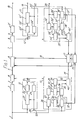
- Referring to Figure 1, illustrating a block diagram of a frame synchronizer for the NTSC television system, an input television picture signal is supplied through a video
signal input terminal 1 to alow pass filter 2 where undesirable high frequencies of the input signal are removed. Then the filtered input signal is sampled in an analogue-to-digital (A/D)converter 4 at a frequency of 10.7 MHz, which is three times the input subcarrier burst frequency, and converted into pulse code modulated (PCM) parallel 8-bit data 5. Further, writeclock pulses 12 and writesubcarrier pulses 25, which are synchronized with the colour burst of the input signal, are formed by a burst controlled oscillator (BCO) 11 comprised of a burst gate/phase comparator 21, a clock pulse generator.23, and a 1/3counter 24. Write-inaddress data 14 synchronized with a synchronizing signal of the input signal is formed by awrite address generator 13. The parallel 8-bit data 5 of one frame period is written in an elasticdigital memory 6 of about 2.4 Mbits, which are designated by the write-inaddress data 14. - A read-out clock pulse 12' and a read-out subcarrier pulse 25' which is synchronized with an external
subcarrier input signal 19, are formed by a read clock generator 11'. Read-out address data 14' synchronized with an external synchronizinginput signal 20 is formed by a read-out address generator 13'. In response to the read-out address data and the read-out clock, the PCM data stored in thememory 6 is read-out and converted into a pulse amplitude modulated (PAM)signal 9 by a digital-to-analogue (D/A)converter 8. ThePAM signal 9 is applied to a low pass filter 2' where spurious high frequency components are filtered out. In this way, atelevision signal 10 synchronized with thereference signals - In the write-in
address generator 13, a composite synchronizingsignal 27 is separated from thecomposite television signal 1 by a synchronizingsignal separator 26. Then, vertical (V)pulses 29 and horizontal (H)pulses 31 are separated from the composite synchronizingsignal 27 by aV pulse separator 28 and anH pulse separator 30, respectively.Frame pulses 33 are formed from theV pulses 29 and theH pulses 31 by aframe pulse generator 32.Vertical address data 35 is formed from theframe pulses 33, theV pulses 29,and theH pulses 31 by avertical address generator 34. - In this example, the number of memory cards used in the
memory 6 is to be n (=6). Further the 8-bitparallel data 5 of three samples, ie one subcarrier cycle, are written in the first memory card, the data for the next subcarrier cycle is written in the second memory card, and so on, and in this way the same amount data is written in each of the subsequent memory cards up to the final card n by the same write-inaddress data 14. Each of the memory cards has three blocks of memory ICs (intergrated circuits) A, B and C. Each block has 8 ICs to allow write-in in 8-bit parallel format. The 8-bitparallel data 5 of three samples for each memory card are written in the respective blocks A, B and C by the same write-inaddress data 14. - An H/V mixed address system has been used which eliminates the assignment of the memory capacity to most of the horizontal blanking period and the vertical blanking period, thereby to form a
memory address 14 for providing a lessened memory capacity. 'Memory card write-in selectingaddress data 37, for making the n memory cards successively subject to the write-in operation during a period of one subcarrier cycle, is formed from theH pulse 31 and the writesubcarrier pulse 25 by acard selecting counter 36. Thewrite address data 14 is changed by one after each cycle -f the write-in sequence of the n memory cards, that is, thehorizontal address data 39 formed in ahorlzontal address generator 38, changes in dependence on the memory card selectingaddress data 37 and on the write-insubcarrier pulse 25. Thevertical address data 35 and thehorizontal address data 39 are mixed by an H/V address mixer 40 thereby to form the write-inaddress data 14. - Similarly, a read address generator 13' forms read-out address data 14' and memory card read-out selecting
address data 37. By using the memory card write-in selectingaddress data 37 and the memory card read-out selecting address data 37', a read/ writecontrol circuit 15 forms read/writecontrol pulses 16 used for read-out and write-in sequence controls of the n memories. A read/write selector 17 is so controlled that, in response to the read/write control pulse 16, it transforms the write-inaddress data 14 into amemory address 18 in the write-in mode while it transforms the read-out address data 14' into thememory address 18 in the read-out mode. - A memory address construction of the known H/V mix address system is illustrated in Fig 2. For one frame of an interlaced television signal of 525 lines per picture at 60 frames per second, the minimum memory capacity for storing 512 scanning lines, each of which is 53.6 µs, is 2.359296 M bits (≠512 lines x 53.6 x 10⁻⁶≠ [1/(3.58 x 106-x 3)) x 8 bits). This minimum memory capacity, 2.359296 M bits, may be constructed by using six memory cards each including 24 memory ICs (= three IC blocks x 8 (bits)), each memory IC having 16.384 K bits. Since the 16.384 K word address is 14 bits (= 9 + 5 bits) a satisfactory memory construction may be obtained with 9 bits ("0" to "511") being assigned to the vertical address and 5 bits ("0" to "31") to the horizontal address. The television signal of each subcarrier cycle, ie of three samples, is stored in the three blocks of one memory card, that is to say, the write-in operations of the three memory IC blocks are performed with one horizontal address..Thus, in the NTSC case shown in Figure 2, the picture memory device with a minimum memory capacity may be realized by using the conventional H/V mixed address system.
- Figure 3 shows a memory address construction in case of the PAL or SECAM colour television system. The sampling frequency of the A/D converter is 13.3 MHz, which (as in the NTSC case) is three times the subcarrier frequency which is now 4.43 MHz, and the PCM data of the A/D converter is of 8-bit parallel format. In the PAL television system of 625 lines per picture and 50 frames per second, the picture information of two fields is stored, omitting the vertical blanking period except that the vertical interval test signals (VITS) in the vertical blanking period are stored. Accordingly, the memory capacity necessary to store 628 scanning lines each of 58.6 µs is 3.912664 M bits (≒ 628 x 58.6 x 10-6 ÷ {1/(4.43 x 106 x 3)} x 8 bits). The minimum number n of the memory cards of 393.216 K bits necessary for 3.912664 M bits, each memory card including 24 memory ICs (= three IC blocks x 8 bits) each having 16.384 K bits, is the next whole number above:

- The 16.384 K word address is 14 bits; however, the vertical address ranges from 0 to 627 and needs 10 bits while the horizontal address ranges 0 to 25 and needs 5 bits. Thus, when the H/V mixed address system is employed for the address formation, a total of 15 bits are necessary. As a result, 20 memory cards, are needed. Further, the utilization efficiency of the memory capacity is:
- (3.912664 x 10⁶/393.216 x 103 x 20) x 100 = 49.7% Thus, the memory efficiency is extremely low.
- In Figure 3, in which the horizontal address axis along the abscissa is represented by h and the vertical address axis along the ordinate by v, a memory capacity of the first memory card is equal to an area enclosed by four coordinates (ho, vo), (h31, vo), (h31, V511), and (ho, v511). However, the memory area actually used is merely an area enclosed by coordinates (ho, vo), (h25, vo), (h25, v511) and (ho, v511). As seen from Figure 3, the portion of the horizontal address axis h ranging from h26 to h3l is not used.
- The memory capacity cf the llth memory card is an memory area enclosed by four coordinates (ho, v512), (h31, v512), (h31, vl023) and (ho, vl023). However,the area actually used is merely an area enclosed by coordinates (ho, v512), (h25, v512), (h25, v627) and (ho, v627).
- The area not used on the first memory card is:


- Thus, the area not used by the first memory card is larger than that actually used in the llth card.
- When considering the above referring to the memory IC of 16.384 K words or 14 bit address, it is seen that . the utilization efficiency of the abscissa is insufficient though the horizintal address is 5 bits, and that the vertical address of 10 bits is larger than 9 bits (= 14 - 5). As a consequence, the utilization efficiencies in the horizontal address axis and the vertical address axis are not balanced. This unbalance causes the above-described low memory efficiency.
- In the present system, the utilization efficiency in the horizontal address axis direction is improved without effectively increasing the bits of an imaginary horizontal address x whereby the bits of an imaginary vertical address y is reduced, eliminating the use of the llth and the subsequent memory cards.
- Figure 4(a) illustrates a conventional memory address updating system using two-dimensional addresses of H and V. The vertical address of the memory address changes every scanning line. In Figure 4(b), serial numbers as memory addresses are assigned in accordance with the order for storing the data into the memory, and there is illustrated how to convert the two-dimensional addresses into one-dimensional
continuous addresses 0 to 16328 (14 bits) in such an order. By comparison with the diagram of Figure 4(a), in an imaginary coordinate system of X and Y of Figure 4(b), the lower 5 bits of the one-dimensionalcontinuous address 14 bits is selected for the abscissa and the upper 9 bits for the ordinate. When comparing these, the increase of the imaginary ordinate address in Figure 4(b) is less rapid. To realise this, the vertical address from the address generator is multiplied by a vertical address multiplier to be increased by m which is the horizontal address number to be changed within one scanning line. Further, the output signal from the multiplier is loaded into the memory address counter at the period of the horizontal pulses and the memory address counter is incremented at the period of the memory card selecting counter. - The operation principle as mentioned above will be described referring to the comparative illustrations of Figures 4(a) and (b). The conversion of the two-dimensional address of H and V into the imaginary one-dimensional continuous address is equivalent to that in Figure 4(a), the h address blocks 0 to 25 at vo are arranged in a line, being followed by the h address blocks 26 to 51 at vl. When the new abscissa X address is 5 bits, it in Figure 4(b) is equivalent to an address construction in which a series of
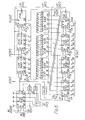
addresses 0 to 16328 (14 bits) are divided into blocks each including the 5-bit maximum value, ie 32 from 0 to 31, for example, and those blocks are stacked in a new ordinate of Y addresses yo, yl, ...., y509 (9 bits), as shown in Figure 4(b). - Referring to Figure 5,
vertical address data 35 from avertical address generator 34 is multiplied by m (26) in avertical address multiplier 41 thereby forming an initial value of the write-instart address data 42 for each scanning line, that is, each H start address data 42 (H = 0). The H startaddress data 42 is given by v x m where v is avertical address data 35 and m ar. address change value necessary for the write-in operation within the H. - In the case of Figure 4(b), for example, in the case of the vertical address vo, since the horizontal write-in
addresses 0 to 25, the address change value necessary for write-in within vo is 26. Then, each H startaddress data 42 is loaded as "load data" into the write-inmemory address counter 43 by anH pulse 31 for determining the write start phase of each H from anH pulse generator 30. Thememory address counter 43, having the write-in start address initial value of each H loaded at the start phase of each H, successively increments the write-inmemory address 14 by one at the period of the most significant bit of acard selecting address 37 which provides a cycle of memory card operation sequences from a memorycard selecting counter 36. The read memory address 14' is formed in a similar manner. - Figure 6 shows a circuit diagram of a detailed part of the embodiment where the present invention is embodied. The respective IC type numbers are shown. The vertical address 35 (35') is formed by the vertical address generator 34 (34') comprised of counters IC44 to 46.
- A multiplier comprised of PROMs (programmable read only memories) IC47 to 49 first increases the vertical address 35 (35') by 13 times and further shifts the output by one bit to double it. The result is multiplication by 13 x 2 = 26. The memory card selection counter 36(36') comprising a counter IC50 and a decoder IC51 cooperate to form a memory card selecting address 37(37'). The memory card selecting counter 36(36') and a decoder IC52 cooperatively form count enable
pulses 57. A write-in start address 42 for each H is loaded as an initial value into the memory address counter 43 (43') comprised of counter ICs 53 to 56 in response to aload control pulse 58 formed from the H pulse 31 (31'). By the count enablepulse 57 of the period corresponding to 10 subcarrier cycles, the memory address 14(14') formed by the memory address counter 43(43') progressively changes by one. - Generally, most of the horizontal blanking period of each H has no need of storage. In the present embodiment. 5.4 ps ( = 64.0 - 58.6) is a no-store period. Even in the no-store period, the memory address data 14 (14') is counted up, so that the load returns it to the normal start address again.
- As described-above, the present invention mainly uses the vertical address generator, the vertical address multiplier, the memory block (card) selecting counter, and the memory address counter, thereby there are advantageous effector of reducing the memory address bit and minimizing the memory capacity.
Claims (3)
Applications Claiming Priority (2)
| Application Number | Priority Date | Filing Date | Title |
|---|---|---|---|
| JP11649079A JPS5640882A (en) | 1979-09-11 | 1979-09-11 | Image memory unit |
| JP116490/79 | 1979-09-11 |
Publications (3)
| Publication Number | Publication Date |
|---|---|
| EP0025364A2 true EP0025364A2 (en) | 1981-03-18 |
| EP0025364A3 EP0025364A3 (en) | 1982-01-13 |
| EP0025364B1 EP0025364B1 (en) | 1984-05-16 |
Family
ID=14688407
Family Applications (1)
| Application Number | Title | Priority Date | Filing Date |
|---|---|---|---|
| EP80303194A Expired EP0025364B1 (en) | 1979-09-11 | 1980-09-11 | Digital television video signal storage system |
Country Status (4)
| Country | Link |
|---|---|
| US (1) | US4325075A (en) |
| EP (1) | EP0025364B1 (en) |
| JP (1) | JPS5640882A (en) |
| DE (1) | DE3067857D1 (en) |
Cited By (1)
| Publication number | Priority date | Publication date | Assignee | Title |
|---|---|---|---|---|
| GB2226733A (en) * | 1988-12-31 | 1990-07-04 | Samsung Electronics Co Ltd | Digital recording of colour television signals |
Families Citing this family (16)
| Publication number | Priority date | Publication date | Assignee | Title |
|---|---|---|---|---|
| JPS57209572A (en) * | 1981-06-19 | 1982-12-22 | Hitachi Ltd | Picture memory device |
| US4580134A (en) * | 1982-11-16 | 1986-04-01 | Real Time Design, Inc. | Color video system using data compression and decompression |
| JPS6020690A (en) * | 1983-07-15 | 1985-02-01 | Sony Corp | Television receiver |
| JPS6076089A (en) * | 1983-09-30 | 1985-04-30 | Nec Corp | Semiconductor memory |
| JPS60106279A (en) * | 1983-11-15 | 1985-06-11 | Sony Corp | Television receiver |
| JP2507319B2 (en) * | 1986-04-23 | 1996-06-12 | 株式会社日立製作所 | Video memory |
| US4857990A (en) * | 1986-06-20 | 1989-08-15 | Computer Devices, Inc. | Digital video storage |
| JPH01255584A (en) * | 1988-04-04 | 1989-10-12 | Mitsubishi Paper Mills Ltd | Heat-sensitive recording material |
| JP2539082B2 (en) * | 1990-07-16 | 1996-10-02 | 富士通株式会社 | Data transfer device |
| US5422678A (en) * | 1991-01-29 | 1995-06-06 | Seiko Epson Corp. | Video processor for enlarging and contracting an image in a vertical direction |
| US5402181A (en) * | 1991-04-01 | 1995-03-28 | Jenison; Timothy P. | Method and apparatus utilizing look-up tables for color graphics in the digital composite video domain |
| JPH0548998A (en) * | 1991-08-08 | 1993-02-26 | Rohm Co Ltd | Image recording device |
| US6469741B2 (en) | 1993-07-26 | 2002-10-22 | Pixel Instruments Corp. | Apparatus and method for processing television signals |
| US6380967B1 (en) | 1996-12-07 | 2002-04-30 | Frank Sacca | System to capture, store, and retrieve composite video for transmission over telephone lines |
| US6563507B1 (en) * | 1999-09-22 | 2003-05-13 | Sony Corporation | Storage circuit control device and graphic computation device |
| JP3751251B2 (en) * | 2002-01-11 | 2006-03-01 | Necディスプレイソリューションズ株式会社 | Video signal processing apparatus and method |
Citations (1)
| Publication number | Priority date | Publication date | Assignee | Title |
|---|---|---|---|---|
| US3860952A (en) * | 1973-07-23 | 1975-01-14 | Cons Video Systems | Video time base corrector |
Family Cites Families (1)
| Publication number | Priority date | Publication date | Assignee | Title |
|---|---|---|---|---|
| US4007486A (en) * | 1974-10-05 | 1977-02-08 | Nippon Electric Co., Ltd. | Phase locking system for television signals using a digital memory technique |
-
1979
- 1979-09-11 JP JP11649079A patent/JPS5640882A/en active Granted
-
1980
- 1980-09-11 EP EP80303194A patent/EP0025364B1/en not_active Expired
- 1980-09-11 US US06/186,209 patent/US4325075A/en not_active Expired - Lifetime
- 1980-09-11 DE DE8080303194T patent/DE3067857D1/en not_active Expired
Patent Citations (3)
| Publication number | Priority date | Publication date | Assignee | Title |
|---|---|---|---|---|
| US3860952A (en) * | 1973-07-23 | 1975-01-14 | Cons Video Systems | Video time base corrector |
| US3860952B1 (en) * | 1973-07-23 | 1995-01-17 | Video Patents Limited | Video time base corrector |
| US3860952B2 (en) * | 1973-07-23 | 1996-05-07 | Harris Corp | Video time base corrector |
Cited By (1)
| Publication number | Priority date | Publication date | Assignee | Title |
|---|---|---|---|---|
| GB2226733A (en) * | 1988-12-31 | 1990-07-04 | Samsung Electronics Co Ltd | Digital recording of colour television signals |
Also Published As
| Publication number | Publication date |
|---|---|
| EP0025364A3 (en) | 1982-01-13 |
| EP0025364B1 (en) | 1984-05-16 |
| JPS5640882A (en) | 1981-04-17 |
| US4325075A (en) | 1982-04-13 |
| DE3067857D1 (en) | 1984-06-20 |
| JPS6343772B2 (en) | 1988-09-01 |
Similar Documents
| Publication | Publication Date | Title |
|---|---|---|
| EP0025364B1 (en) | Digital television video signal storage system | |
| US4134128A (en) | Television picture size altering apparatus | |
| US4855833A (en) | Television channel selection apparatus employing multi-picture display | |
| US4831441A (en) | Scan converter apparatus | |
| US5426468A (en) | Method and apparatus utilizing look-up tables for color graphics in the digital composite video domain | |
| US4218710A (en) | Digital video effect system comprising only one memory of a conventional capacity | |
| US4316219A (en) | Synchronizing circuit adaptable for various TV standards | |
| US4500908A (en) | Method and apparatus for standardizing nonstandard video signals | |
| EP0356453B1 (en) | Interpolator for expanding video data | |
| US5410357A (en) | Scan converter and method | |
| EP0245745A2 (en) | Image processing system | |
| US4218700A (en) | Luminance/chrominance separating apparatus having a spatial filtering effect | |
| EP0122561A2 (en) | Television video signal synchronizing apparatus | |
| US4970588A (en) | Video monitoring apparatus with plural inputs | |
| US4531147A (en) | Digital memory color framing circuit | |
| US5629962A (en) | Phase locked loop circuit | |
| US3863022A (en) | Television signal clocked delay line for delay by an integer number of horizontal scanning lines driven by a pilot signal | |
| US4412250A (en) | Memory-type sync generator with reduced memory requirements | |
| EP0037230A1 (en) | Video signal recording and/or reproducing system | |
| US4701800A (en) | Scanning line position control system for shifting the position of scanning lines to improve photographic reproduction quality | |
| EP0056052B1 (en) | Synchronizing circuit adaptable for various tv standards | |
| EP0153861A2 (en) | Video signal delay circuit | |
| US6329982B1 (en) | Programmable pulse generator | |
| US5053863A (en) | Circuit for processing digital video signals | |
| US5534939A (en) | Digital video clock generation system |
Legal Events
| Date | Code | Title | Description |
|---|---|---|---|
| PUAI | Public reference made under article 153(3) epc to a published international application that has entered the european phase |
Free format text: ORIGINAL CODE: 0009012 |
|
| AK | Designated contracting states |
Designated state(s): DE FR GB NL |
|
| PUAL | Search report despatched |
Free format text: ORIGINAL CODE: 0009013 |
|
| AK | Designated contracting states |
Designated state(s): DE FR GB NL |
|
| 17P | Request for examination filed |
Effective date: 19820709 |
|
| RAP1 | Party data changed (applicant data changed or rights of an application transferred) |
Owner name: NEC CORPORATION |
|
| GRAA | (expected) grant |
Free format text: ORIGINAL CODE: 0009210 |
|
| AK | Designated contracting states |
Designated state(s): DE FR GB NL |
|
| REF | Corresponds to: |
Ref document number: 3067857 Country of ref document: DE Date of ref document: 19840620 |
|
| ET | Fr: translation filed | ||
| PLBE | No opposition filed within time limit |
Free format text: ORIGINAL CODE: 0009261 |
|
| STAA | Information on the status of an ep patent application or granted ep patent |
Free format text: STATUS: NO OPPOSITION FILED WITHIN TIME LIMIT |
|
| 26N | No opposition filed | ||
| PGFP | Annual fee paid to national office [announced via postgrant information from national office to epo] |
Ref country code: GB Payment date: 19910809 Year of fee payment: 12 |
|
| PGFP | Annual fee paid to national office [announced via postgrant information from national office to epo] |
Ref country code: FR Payment date: 19910913 Year of fee payment: 12 |
|
| PGFP | Annual fee paid to national office [announced via postgrant information from national office to epo] |
Ref country code: NL Payment date: 19910930 Year of fee payment: 12 |
|
| PGFP | Annual fee paid to national office [announced via postgrant information from national office to epo] |
Ref country code: DE Payment date: 19911128 Year of fee payment: 12 |
|
| PG25 | Lapsed in a contracting state [announced via postgrant information from national office to epo] |
Ref country code: GB Effective date: 19920911 |
|
| PG25 | Lapsed in a contracting state [announced via postgrant information from national office to epo] |
Ref country code: NL Effective date: 19930401 |
|
| GBPC | Gb: european patent ceased through non-payment of renewal fee |
Effective date: 19920911 |
|
| NLV4 | Nl: lapsed or anulled due to non-payment of the annual fee | ||
| PG25 | Lapsed in a contracting state [announced via postgrant information from national office to epo] |
Ref country code: FR Effective date: 19930528 |
|
| PG25 | Lapsed in a contracting state [announced via postgrant information from national office to epo] |
Ref country code: DE Effective date: 19930602 |
|
| REG | Reference to a national code |
Ref country code: FR Ref legal event code: ST |