EP0024902B1 - Apparatus and method for converting one-bit image data into gray scale image data - Google Patents
Apparatus and method for converting one-bit image data into gray scale image data Download PDFInfo
- Publication number
- EP0024902B1 EP0024902B1 EP80302925A EP80302925A EP0024902B1 EP 0024902 B1 EP0024902 B1 EP 0024902B1 EP 80302925 A EP80302925 A EP 80302925A EP 80302925 A EP80302925 A EP 80302925A EP 0024902 B1 EP0024902 B1 EP 0024902B1
- Authority
- EP
- European Patent Office
- Prior art keywords
- bits
- columns
- rows
- bit
- difference
- Prior art date
- Legal status (The legal status is an assumption and is not a legal conclusion. Google has not performed a legal analysis and makes no representation as to the accuracy of the status listed.)
- Expired
Links
- 238000000034 method Methods 0.000 title claims description 15
- 239000011159 matrix material Substances 0.000 claims description 15
- 238000012937 correction Methods 0.000 claims description 11
- 230000008569 process Effects 0.000 description 10
- 238000004364 calculation method Methods 0.000 description 9
- 230000007704 transition Effects 0.000 description 8
- 239000000872 buffer Substances 0.000 description 7
- 238000000605 extraction Methods 0.000 description 7
- 238000001914 filtration Methods 0.000 description 4
- 238000007792 addition Methods 0.000 description 3
- 230000008094 contradictory effect Effects 0.000 description 3
- 230000006870 function Effects 0.000 description 3
- 230000010354 integration Effects 0.000 description 3
- 101100521334 Mus musculus Prom1 gene Proteins 0.000 description 2
- 230000008901 benefit Effects 0.000 description 2
- 238000010586 diagram Methods 0.000 description 2
- 230000015654 memory Effects 0.000 description 2
- 238000012935 Averaging Methods 0.000 description 1
- 230000008859 change Effects 0.000 description 1
- 239000003086 colorant Substances 0.000 description 1
- 238000013461 design Methods 0.000 description 1
- 230000000694 effects Effects 0.000 description 1
- 206010016256 fatigue Diseases 0.000 description 1
- 230000001788 irregular Effects 0.000 description 1
- 238000004519 manufacturing process Methods 0.000 description 1
- 238000012545 processing Methods 0.000 description 1
- 230000008672 reprogramming Effects 0.000 description 1
- 230000000630 rising effect Effects 0.000 description 1
- 238000012216 screening Methods 0.000 description 1
- 230000000007 visual effect Effects 0.000 description 1
Images


Classifications
-
- H—ELECTRICITY
- H04—ELECTRIC COMMUNICATION TECHNIQUE
- H04N—PICTORIAL COMMUNICATION, e.g. TELEVISION
- H04N1/00—Scanning, transmission or reproduction of documents or the like, e.g. facsimile transmission; Details thereof
- H04N1/40—Picture signal circuits
- H04N1/409—Edge or detail enhancement; Noise or error suppression
- H04N1/4092—Edge or detail enhancement
-
- G06T5/92—
-
- H—ELECTRICITY
- H04—ELECTRIC COMMUNICATION TECHNIQUE
- H04N—PICTORIAL COMMUNICATION, e.g. TELEVISION
- H04N1/00—Scanning, transmission or reproduction of documents or the like, e.g. facsimile transmission; Details thereof
- H04N1/40—Picture signal circuits
- H04N1/40075—Descreening, i.e. converting a halftone signal into a corresponding continuous-tone signal; Rescreening, i.e. combined descreening and halftoning
Definitions
- the copy comprises a matrix of black and white dots.
- the black dots are increased in size relative to the white dots to represent areas of darker gray while the size of the white dots are relatively increased to represent lighter shades of gray.
- a more difficult problem occurs where the original itself is a halftone representation, rather than a photograph or equivalent.
- the production of a halftone copy from a halftone original usually results in a degraded copy because the original generates a large amount of non-informational content which, consequently, reacts with the copying process to produce Moire patterns, irregular shape and size of dots and a loss of texture and gray scale.
- the most common method of improving the quality of reproduction from a halftone original is to filter out those screen frequencies that are produced by the halftoning process.
- the apparatus in raster scanning systems typically comprises a raster input scanner for converting the halftone original into an analog voltage, an analog filter to attenuate the high frequencies of the electrical signal, a halftone screener to convert the analog voltage into a halftone representation, and a printing engine to produce the hard copy.
- One problem with this system is that the filtering out of the screen frequencies by a low-pass filter also filters out most of the highlights and sharp edges that would otherwise have been reproduced in the copy. The result is a halftone reproduction that has an unfocused or washed-out look.
- An alternative system converts the raster input scanner analog voltage into a digital representation, typically six bits or more per pixel. This data stream is then operated on by some type of two-dimensional digital filter to filter out the halftone screen frequencies. This process is time-consuming and requires a relatively large amount of hardware since the digital representation of each pixel is typically multiplied by a weighting factor as part of the filtering process. The digital realization of low-pass filtering also results in the loss of highlights and sharp edges.
- Hell1 discloses using a low-pass filter and an adder circuit for acting on the signals produced by scanning a continuous-tone image in order to retain or enhance the reproduction of boundaries in the original.
- the apparatus of the present invention starts with a halftone image and uses an edge-extraction circuit to determine the rate at which a rectangular bit matrix centered on the pixel in question is in transition from white to black, and predominantly horizontally or vertically.
- the present invention therefore aims at producing a high speed method and apparatus for reproducing halftone images which may be implemented in a relatively simple circuit and which maintains a reasonable amount of detail in the copy.
- the halftone rescreening method described herein comprises a raster input scanner which converts the halftone image into an analog voltage. This voltage is then thresholded to produce a one-bit per pixel video signal which is used as the input to two paths of the rescreening circuit, an area integration path and an edge-extraction path.
- the thresholding of the input video into a one bit per pixel digital representation represents no more than a slight loss of information since the color values in the original are either black or white, and the scanning resolution is at least four times the half- tone screen frequency. There may be a loss of information when the point being scanned is a transition point between a white and a black dot. In this case, the analog representation must be thresholded into a one-bit black or white pixel. The pixels involved are few in number and are compensated for by a relatively large area of integration.
- the area integrator in the described embodiment, sums the one and zero bits in a nine- by-seven bit area surrounding the pixel in question to yield a value of from zero to sixty-three, which is represented as a six-bit word.
- the edge-extraction circuit uses a more complex algorithm which determines the rate at which a six-by-seven bit matrix surrounding the pixel in question is in an edge transition from white to black or black to white, and further determines whether this transition is occurring horizontally or vertically. This algorithm determines from these matrices the direction and rate of variation, and produces therefrom a five-bit (plus sign) signal representing the direction and rate of change of the image edge.
- the final step is to add the area integration output with the edge extraction output, resulting in a six bit per pixel signal varying from zero to sixty-three.
- This gray scale representation of the original now contains a minimum of Moire patterns, provides greater image detail and sharp edges and is in a form that can be fed to either a thresholding device or a halftone screener of any kind to produce a hard copy. Because there is no weighting of gray scale information, as is required in the normal digital filtering process, the circuit required to implement this rescreening process is relatively simple and can be implemented to operate at high speeds. In addition, the resultant halftone copy is a reasonably-faithful reproduction of the original, having a minimum of Moire patterns and reasonable gray scale and edge sharpness.
- Waveshape 1 A is a representation of the output that would result if an original continuous tone photograph were scanned by a raster-input-scanning type device as the raster moved across an abrupt threshold between a light gray and a dark gray area. Assuming a full scale variation of from zero to sixty-three corresponding to a variation from white to black, waveshape 1A then is a waveshape of an analog voltage transition from light gray to dark gray.
- the original is assumed to be a halftone original and there is the further assumption that the scanner output will be thresholded. Therefore, the actual "original” signal will be "zero" where the light gray portion of the Figure 1 A voltage has a predominance of white or zero pixels and "one" where the darker portion has a predominance of one or black pixels. This one bit per pixel signal is applied to the circuit of Figure 2.
- the area integrator 120 of Figure 2 passes the waveshape of the original edge 1A through a low-pass filter to produce the waveshape of 1B. Simultaneously, the original edge 1 A is applied to an edge extraction circuit 121 to produce the detected edge waveshape 1 C. Finally, waveshapes 1 B and 1C are added together in the summing junction 122 of Figure 2 to produce an enhanced edge waveshape as shown in Figure 1 D.
- the waveshapes of Figure 1 A through 1 D are shown in analog form but are, in all cases, digital signals.
- the original edge 1 A is a one bit per pixel halftone representation of the original halftone image.
- Figure 1 B is a six bit digital representation of the image produced by the area integrator varying from zero to sixty-three.
- Figure 1 C is a series of five bits, including sign, per pixel representing the detected edge in a positive or negative direction, theoretically averaging zero.
- the Figure 1 D waveshape is the summation of waveshapes 1 B and 1 C and is represented as a series of six bit digital numbers varying from zero to sixty-three.
- the summation of waveshapes 1B and 1 C may be a simple arithmetic addition, but it also may be a complex function. In any case, the result of the summation step is limited, as shown in Figure 1 D, to a numerical value of between zero and sixty-three as shown. No significant loss of information results from this limitation since the actual image data in purely white or black will not be degraded by the limitation.
- the output of the summation junction 122 is a six bit per pixel gray scale representation and may be thresholded, screened, or used directly in any printing process.
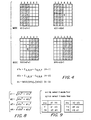
- Figure 3 is a representation of the process by which the area integrator 20 calculates a value for each pixel.
- the value for each pixel, labeled N in Figure 3 is determined by the simple counting of the "one" bits contained in the seven-by-nine bit area surrounding the pixel in question.
- this 7 x 9 bit area typically includes two white and two black halftone dots for a range of scanning and screening resolutions.
- the raster input scanner produces 19 pixels per mm so that the image pattern shown in Figure 3 would result from the scanning of a half-tone original containing approximately 2 dots per mm horizontally.
- An area integrator works properly if the area includes at least two white and two black dots as shown in Figure 3. Therefore, this particular embodiment will operate properly on halftone screens for approximately 20 dots or more per mm.
- halftone screens containing fewer than 2 dots per mm, and text do not require rescreening.
- the numerical choices made for this embodiment are optimum for practical purposes.
- Another advantage of the choice of a 7 x 9 bit pixel is that there is an odd number of bits in both directions to allow for the processing of a center pixel, and also that the sum of the bits contained within this matrix may be represented by an exact 6-bit binary number.
- the area integrator simply adds the number of bits in the matrix, and couples it to the summing junction 22 of Figure 2.
- the edge-extraction circuit 21 of Figure 2 operates according to the equations shown in Figures 4 and 5.
- the first operation is to determine whether the bit in question, N, is located at a vertical edge, is going from black to white or white to black, and to determine a numerical value of the rate of transition from black to white or white to black. This is done by generating a first set of intermediate values, d1x x and d2x as shown in Figure 4.
- C 2,3,4 - C 5,6,7 is computed by summing the number of black pixels in columns 2, 3, 4 or columns 5, 6 and 7, respectively, of Figure 3.
- the particular sections of the Figure 3 matrix being operated on are shown in Figure 4, the four possible modes labelled X1 through X4.
- the difference between modes X1 and X3 is that X1 will result in a positive number, showing a transition from black to white, while X3 will result in a negative number, showing a transition from white to black.
- d 1 x is defined as the sum of columns 2,3 and 4 minus the sum of columns 5, 6 and 7 as shown in equation (4-1).
- the absolute magnitude of the number will be an indication of the slope of the edge, corresponding to the slope of the rising edge of the waveshape in Figure 1 A.
- the calculation of d2x is similar to the calculation of d 1x except that columns 1 through 6 of Figure 3 are used instead of columns 2 through 7.
- the portions of the matrix of Figure 3 being operated on to calculate d2x are shown as X2 and X4 and the equation used to calculate 'd2x is labelled (4-2).
- a value dx is set equal to the larger of the absolute value of d1x and the absolute value of d2x.
- edge enhancement is computed as shown in Figure 6.
- Figure 9 is a shortened summary of Figures 6 and 7, and shows which correction values (d1 through d4) will be used for the various modes.
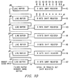
- FIG 10 is a schematic of the line buffers 20 used to supply data to a bank of seven 9-bit shift registers 21.
- Each line buffer 20 contains 5280 or more bits, which is the contents of at least one entire 275 mm raster scan. Therefore, a total of seven raster scan lines are contained in the line buffers 20.
- a bit is clocked from each line buffer, into the next buffer and into each register 21.
- the contents of the entire bank of shift registers 21 are the data required by the matrices of Figures 3, 4 and 5.
- Each register 21 has nine output lines CO through C8, to supply a seven-by-nine bit matrix of values to the remainder of the circuit.
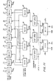
- the edge-enhancement value in the X (column) direction is calculated by the circuit of Figure 11. An identical circuit, not shown, is used to calculate the Y (row) edge enhancement value.
- ROMs 25a and 25b which are implemented as adders to compute either C 1,2,3 - C 4,5,6 as in equation (4-2), or C 2,3,4 - C 5,6,7 as in equation (4-1) of Figure 6.
- the difference can be a maximum of 21 plus sign, which normally requires a six-bit output.
- the 21 possible outputs are mapped to 16 outputs (plus sign) to allow each ROM 25a and 25b to have a five-bit output for simple implementation.
- the 16 outputs represent the number of steps of extracted edge rather than the hexadecimal representation of 4 bits. The exact values of the edge steps are stored in ROM 33.
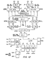
- First ROMs 26 compare the absolute values of d2x and d 1 and d2y to d1y, and in each case, select the larger. These two outputs are then latched through latches 27 and are compared at comparator 28, the output of which is a one-bit flag indicating whether the X or Y value is larger.
- ROM 29 receives all four sign bits (d1x, d2x, d1y, d2y) from latches 27, bits indicating whether d 1 x or d2x (and d 1 y or d2y) is larger, and the bit from comparator 28 indicating whether the greatest absolute value is an X or Y value, and uses these to determine which line in the tables of Figures 6 and 7 to use for edge enhancement.
- the comparator 28 output determines whether the Figure 6 or Figure 7 table should be used, and within the appropriate table, the max bits at the ROM 26 outputs in conjunction with the two sign bits for each latch 27 narrow the choice to one line of the selected table.
- the final step is to calculate the ultimate edge correction which is of the form N ⁇ dxy.
- ROM 29 controls each multiplexer 30 to couple the correct values of dx and dy from latches 31 through latch 32 to ROM 33.
- This ROM 33 is implemented to calculate the root mean square, accomplishing the selected calculation of Figure 8.
- N the outputs of the C0, C1 and C8 ROMs 22 of Figure 11 are added in ROM 34 to form a subtotal which is latched through latch 35 and added in ROM 36 to the output of ROM 37 which has added the C 2.3.4 and C S.6 . 7 values which are available at the output of Figure 11 ROMs 23.
- the resultant output of ROM 36 is a value of N which is latched through latches 37 and 38 and to which is either added or subtracted the value of the dxy output from ROM 33.
- the sign of this operation is determined by the "dxy sign" output bit from ROM 29.
- ROM devices are used for a variety of functions that could have been performed by other types of devices.
- the function of ROMs 22 could have been performed by encoders.
- ALUs could have been used instead of ROMs 25 and memory devices used instead of buffers 20 and shift registers 21.
- the operation of the circuit would remain unchanged in that the calculations of Figure 7 would be performed in any case.
- ROMs have been selected for this embodiment because of the higher speed and lower cost of these devices.
- the root mean square need not be limited to the exact mathematical value, but may be varied, by reprogramming the ROM to shade the output in any way to give a better ultimate copy, and also to eliminate small edge variations due to the halftone dots by zeroing out certain PROM locations.
- the various additions and subtractions may also be varied similarly.
- PROMs can be programmed at any point in the design cycle to "tune" the system to various input or output parameters. Decoders and ALUs can be made to vary their outputs only by costly circuit redesign.
Description
- A frequent requirement in the copying, duplicating and printing industry is the reproduction of a continuous tone image, such as that produced through photography, on a printer which is incapable of reproducing gray colors. Newspaper printers and office copiers are the most common examples. A reasonable reproduction of gray scale originals can be accomplished through the process of halftoning. In this case, the copy comprises a matrix of black and white dots. The black dots are increased in size relative to the white dots to represent areas of darker gray while the size of the white dots are relatively increased to represent lighter shades of gray.
- A more difficult problem occurs where the original itself is a halftone representation, rather than a photograph or equivalent. The production of a halftone copy from a halftone original usually results in a degraded copy because the original generates a large amount of non-informational content which, consequently, reacts with the copying process to produce Moire patterns, irregular shape and size of dots and a loss of texture and gray scale.
- The most common method of improving the quality of reproduction from a halftone original is to filter out those screen frequencies that are produced by the halftoning process. The apparatus in raster scanning systems typically comprises a raster input scanner for converting the halftone original into an analog voltage, an analog filter to attenuate the high frequencies of the electrical signal, a halftone screener to convert the analog voltage into a halftone representation, and a printing engine to produce the hard copy. One problem with this system is that the filtering out of the screen frequencies by a low-pass filter also filters out most of the highlights and sharp edges that would otherwise have been reproduced in the copy. The result is a halftone reproduction that has an unfocused or washed-out look.
- An alternative system converts the raster input scanner analog voltage into a digital representation, typically six bits or more per pixel. This data stream is then operated on by some type of two-dimensional digital filter to filter out the halftone screen frequencies. This process is time-consuming and requires a relatively large amount of hardware since the digital representation of each pixel is typically multiplied by a weighting factor as part of the filtering process. The digital realization of low-pass filtering also results in the loss of highlights and sharp edges.
- DE-B-1 268 657 (Hell1 discloses using a low-pass filter and an adder circuit for acting on the signals produced by scanning a continuous-tone image in order to retain or enhance the reproduction of boundaries in the original. In contrast, the apparatus of the present invention starts with a halftone image and uses an edge-extraction circuit to determine the rate at which a rectangular bit matrix centered on the pixel in question is in transition from white to black, and predominantly horizontally or vertically.
- The present invention therefore aims at producing a high speed method and apparatus for reproducing halftone images which may be implemented in a relatively simple circuit and which maintains a reasonable amount of detail in the copy.
- The halftone rescreening method described herein comprises a raster input scanner which converts the halftone image into an analog voltage. This voltage is then thresholded to produce a one-bit per pixel video signal which is used as the input to two paths of the rescreening circuit, an area integration path and an edge-extraction path. The thresholding of the input video into a one bit per pixel digital representation represents no more than a slight loss of information since the color values in the original are either black or white, and the scanning resolution is at least four times the half- tone screen frequency. There may be a loss of information when the point being scanned is a transition point between a white and a black dot. In this case, the analog representation must be thresholded into a one-bit black or white pixel. The pixels involved are few in number and are compensated for by a relatively large area of integration.
- The area integrator, in the described embodiment, sums the one and zero bits in a nine- by-seven bit area surrounding the pixel in question to yield a value of from zero to sixty-three, which is represented as a six-bit word.
- The edge-extraction circuit uses a more complex algorithm which determines the rate at which a six-by-seven bit matrix surrounding the pixel in question is in an edge transition from white to black or black to white, and further determines whether this transition is occurring horizontally or vertically. This algorithm determines from these matrices the direction and rate of variation, and produces therefrom a five-bit (plus sign) signal representing the direction and rate of change of the image edge.
- The final step is to add the area integration output with the edge extraction output, resulting in a six bit per pixel signal varying from zero to sixty-three. This gray scale representation of the original now contains a minimum of Moire patterns, provides greater image detail and sharp edges and is in a form that can be fed to either a thresholding device or a halftone screener of any kind to produce a hard copy. Because there is no weighting of gray scale information, as is required in the normal digital filtering process, the circuit required to implement this rescreening process is relatively simple and can be implemented to operate at high speeds. In addition, the resultant halftone copy is a reasonably-faithful reproduction of the original, having a minimum of Moire patterns and reasonable gray scale and edge sharpness.
- The present invention will now be described by way of example with reference to the accompanying drawings, in which:
- Figures 1 A through 1D are waveshapes drawn to show clearly the effect of an edge-enhancement process in one dimension;
- Figure 2 is an overall block diagram of the apparatus of the present invention;
- Figure 3 is a typical seven-by-nine bit original image section;
- Figure 4 shows vertical edge calculations;
- Figure 5 shows horizontal edge calculations;
- Figure 6 is a matrix of computation to be used when the X mode predominates;
- Figure 7 is a matrix of computations to be used when the Y mode predominates;
- Figures 8 and 9 are a set of equations to determine mode selection; and
- Figures 10, 11 and 12 are schematic diagrams of the circuit used.
- The theory of this invention may be mostly described in relation to the voltage waveshapes of Figures 1 A through 1D. Waveshape 1 A is a representation of the output that would result if an original continuous tone photograph were scanned by a raster-input-scanning type device as the raster moved across an abrupt threshold between a light gray and a dark gray area. Assuming a full scale variation of from zero to sixty-three corresponding to a variation from white to black, waveshape 1A then is a waveshape of an analog voltage transition from light gray to dark gray.
- In terms of this invention the original is assumed to be a halftone original and there is the further assumption that the scanner output will be thresholded. Therefore, the actual "original" signal will be "zero" where the light gray portion of the Figure 1 A voltage has a predominance of white or zero pixels and "one" where the darker portion has a predominance of one or black pixels. This one bit per pixel signal is applied to the circuit of Figure 2.
- The
area integrator 120 of Figure 2 passes the waveshape of the original edge 1A through a low-pass filter to produce the waveshape of 1B. Simultaneously, the original edge 1 A is applied to anedge extraction circuit 121 to produce the detectededge waveshape 1 C. Finally, waveshapes 1 B and 1C are added together in thesumming junction 122 of Figure 2 to produce an enhanced edge waveshape as shown in Figure 1 D. - The waveshapes of Figure 1 A through 1 D are shown in analog form but are, in all cases, digital signals. As explained above, the original edge 1 A is a one bit per pixel halftone representation of the original halftone image. Figure 1 B is a six bit digital representation of the image produced by the area integrator varying from zero to sixty-three. Figure 1 C is a series of five bits, including sign, per pixel representing the detected edge in a positive or negative direction, theoretically averaging zero. Finally, the Figure 1 D waveshape is the summation of waveshapes 1 B and 1 C and is represented as a series of six bit digital numbers varying from zero to sixty-three.
- The summation of waveshapes 1B and 1 C, as will be described below, may be a simple arithmetic addition, but it also may be a complex function. In any case, the result of the summation step is limited, as shown in Figure 1 D, to a numerical value of between zero and sixty-three as shown. No significant loss of information results from this limitation since the actual image data in purely white or black will not be degraded by the limitation.
- As shown in Figure 2 the output of the
summation junction 122 is a six bit per pixel gray scale representation and may be thresholded, screened, or used directly in any printing process. - Figure 3 is a representation of the process by which the
area integrator 20 calculates a value for each pixel. The value for each pixel, labeled N in Figure 3, is determined by the simple counting of the "one" bits contained in the seven-by-nine bit area surrounding the pixel in question. - As shown in Figure 3, this 7 x 9 bit area typically includes two white and two black halftone dots for a range of scanning and screening resolutions. To use the described embodiment as a numerical example, the raster input scanner produces 19 pixels per mm so that the image pattern shown in Figure 3 would result from the scanning of a half-tone original containing approximately 2 dots per mm horizontally. An area integrator works properly if the area includes at least two white and two black dots as shown in Figure 3. Therefore, this particular embodiment will operate properly on halftone screens for approximately 20 dots or more per mm. On the other hand, halftone screens containing fewer than 2 dots per mm, and text, do not require rescreening. Thus, the numerical choices made for this embodiment are optimum for practical purposes.
- Another advantage of the choice of a 7 x 9 bit pixel is that there is an odd number of bits in both directions to allow for the processing of a center pixel, and also that the sum of the bits contained within this matrix may be represented by an exact 6-bit binary number.
- The area integrator simply adds the number of bits in the matrix, and couples it to the summing
junction 22 of Figure 2. - The edge-
extraction circuit 21 of Figure 2 operates according to the equations shown in Figures 4 and 5. The first operation is to determine whether the bit in question, N, is located at a vertical edge, is going from black to white or white to black, and to determine a numerical value of the rate of transition from black to white or white to black. This is done by generating a first set of intermediate values, d1x x and d2x as shown in Figure 4. - The value of C2,3,4 - C5,6,7 is computed by summing the number of black pixels in
columns columns columns columns columns 1 through 6 of Figure 3 are used instead ofcolumns 2 through 7. The portions of the matrix of Figure 3 being operated on to calculate d2x are shown as X2 and X4 and the equation used to calculate 'd2x is labelled (4-2). Finally, as shown in equation (4-3), a value dx is set equal to the larger of the absolute value of d1x and the absolute value of d2x. - The magnitude and direction of the horizontal edge is computed similarly, as shown in Modes Y1 through Y4 and in equations (4-4) through (4-6).
- At this point, it should be noticed that the results of equations (4-1) through (4-6) may or may not be contradictory. For instance, if the calculations show that pixel N is on the black side of a vertical edge as shown in Mode X1 and on the upper black side of a horizontal edge as shown in Mode Y1 there is no contradiction, in either case a black edge correction will be added at pixel N. That is to say, in terms of Figure 2, a black edge correction generated at the
edge extraction block 21 will be added to the output of thearea integrator 20. On the other hand, if the calculations show that the pixel in question, N, is on the white side of a vertical edge as shown in mode X2, but on the black side a horizontal edge is shown in mode Y1, there is some question as to whether the correction for pixel N should be black or white. These alternatives have been provided for in this embodiment using rules which will be explained below. - After determining the numerical value of each mode (X1 through Y4) and the maximum X and Y modes (dx and dy), the equations of Figures 6, 7 and 8 can be used to compute the value of edge enhancement to be added to the final image.
- If dx is greater than or equal to dy (if the absolute value of any one mode is greater than or equal to any of the Y mode absolute values) then the edge enhancement is computed as shown in Figure 6.
- First the identity of the X mode with the highest value is selected. Let us assume that X1 is selected, narrowing the selection to the first two lines of Figure 6. Next, the values of Y1 and Y4 are inspected. At this point, it should be noted that the corrections of modes X1, Y1 and Y4 are non-contradictory. All of these modes result in a black edge enhancement. In other words, the edge enhancement algorithm described herein ignores contradictory corrections. To continue with the example, assume the value of Y1 is greater than Y4. Then the first line of Figure 6 is selected. The final computation becomes N (the integrated area) + dxy where dxy=d1.
- If, initially, dy is greater than dx, the table of Figure 7 would be used in similar fashion. In all cases, the result is the addition or subtraction of a correction value (d1 through d4) to N. Finally, these d1 to d4 values are computed as shown in Figure 8. The computed value is only a rough guideline for edge enhancement. The actual edge correction value can be determined empirically and stored in a programmable read-only memory (PROM).
- Figure 9 is a shortened summary of Figures 6 and 7, and shows which correction values (d1 through d4) will be used for the various modes.
- Figure 10 is a schematic of the line buffers 20 used to supply data to a bank of seven 9-bit shift registers 21. Each
line buffer 20 contains 5280 or more bits, which is the contents of at least one entire 275 mm raster scan. Therefore, a total of seven raster scan lines are contained in the line buffers 20. As each bit is shifted into the first line buffer, a bit is clocked from each line buffer, into the next buffer and into eachregister 21. Thus, the contents of the entire bank ofshift registers 21 are the data required by the matrices of Figures 3, 4 and 5. Eachregister 21 has nine output lines CO through C8, to supply a seven-by-nine bit matrix of values to the remainder of the circuit. - The edge-enhancement value in the X (column) direction is calculated by the circuit of Figure 11. An identical circuit, not shown, is used to calculate the Y (row) edge enhancement value.
- Nine outputs, CO through C8, from each of a total of seven
shift registers 21 are coupled to nine (read-only memories)ROMs 22 implemented as decoders to convert the number of bits, up to a maximum of seven, into the corresponding octal number. The outputs of these decoder ROMs are then used as address inputs to a second row ofROMs 23 which are implemented as adders to supply a total. As indicated in the figure, oneROM 23 is addressed to supply the C1, C2, C3 sum, the next supplies the C4, C5, C6 sum, etc. However, the 21 possible outputs ofROM 23 are represented by a 5 bit output. The resultant total of 20 bits from 4 ROMs is then latched intolatches 24 prior to being input to ROMs 25a and 25b which are implemented as adders to compute either C1,2,3 - C4,5,6 as in equation (4-2), or C2,3,4 - C5,6,7 as in equation (4-1) of Figure 6. The difference can be a maximum of 21 plus sign, which normally requires a six-bit output. However, the 21 possible outputs are mapped to 16 outputs (plus sign) to allow each ROM 25a and 25b to have a five-bit output for simple implementation. The 16 outputs represent the number of steps of extracted edge rather than the hexadecimal representation of 4 bits. The exact values of the edge steps are stored inROM 33. - The remainder of the circuit is shown in Figure 12.
First ROMs 26 compare the absolute values of d2x andd 1 and d2y to d1y, and in each case, select the larger. These two outputs are then latched throughlatches 27 and are compared atcomparator 28, the output of which is a one-bit flag indicating whether the X or Y value is larger. - Finally,
ROM 29 receives all four sign bits (d1x, d2x, d1y, d2y) fromlatches 27, bits indicating whether d 1 x or d2x (and d 1 y or d2y) is larger, and the bit fromcomparator 28 indicating whether the greatest absolute value is an X or Y value, and uses these to determine which line in the tables of Figures 6 and 7 to use for edge enhancement. - Specifically, the
comparator 28 output determines whether the Figure 6 or Figure 7 table should be used, and within the appropriate table, the max bits at theROM 26 outputs in conjunction with the two sign bits for eachlatch 27 narrow the choice to one line of the selected table. - The final step is to calculate the ultimate edge correction which is of the form N ± dxy. First,
ROM 29 controls each multiplexer 30 to couple the correct values of dx and dy fromlatches 31 throughlatch 32 toROM 33. ThisROM 33 is implemented to calculate the root mean square, accomplishing the selected calculation of Figure 8. - To compute N, the outputs of the C0, C1 and
C8 ROMs 22 of Figure 11 are added inROM 34 to form a subtotal which is latched throughlatch 35 and added inROM 36 to the output ofROM 37 which has added the C2.3.4 and CS.6.7 values which are available at the output of Figure 11ROMs 23. The resultant output ofROM 36 is a value of N which is latched throughlatches ROM 33. The sign of this operation is determined by the "dxy sign" output bit fromROM 29. - In these schematics, ROM devices are used for a variety of functions that could have been performed by other types of devices. For instance, the function of
ROMs 22 could have been performed by encoders. Similarly, ALUs could have been used instead ofROMs 25 and memory devices used instead ofbuffers 20 and shift registers 21. However, the operation of the circuit would remain unchanged in that the calculations of Figure 7 would be performed in any case. ROMs have been selected for this embodiment because of the higher speed and lower cost of these devices. - The calculations described above may also be varied to improve the visual results. For example, the root mean square need not be limited to the exact mathematical value, but may be varied, by reprogramming the ROM to shade the output in any way to give a better ultimate copy, and also to eliminate small edge variations due to the halftone dots by zeroing out certain PROM locations. The various additions and subtractions may also be varied similarly. There is a significant advantage in the use of PROMs over ALUs, decoders, etc., since PROMs can be programmed at any point in the design cycle to "tune" the system to various input or output parameters. Decoders and ALUs can be made to vary their outputs only by costly circuit redesign.
Claims (5)
Applications Claiming Priority (2)
| Application Number | Priority Date | Filing Date | Title |
|---|---|---|---|
| US06/069,444 US4259694A (en) | 1979-08-24 | 1979-08-24 | Electronic rescreen technique for halftone pictures |
| US69444 | 1979-08-24 |
Publications (3)
| Publication Number | Publication Date |
|---|---|
| EP0024902A2 EP0024902A2 (en) | 1981-03-11 |
| EP0024902A3 EP0024902A3 (en) | 1981-12-02 |
| EP0024902B1 true EP0024902B1 (en) | 1984-12-27 |
Family
ID=22089010
Family Applications (1)
| Application Number | Title | Priority Date | Filing Date |
|---|---|---|---|
| EP80302925A Expired EP0024902B1 (en) | 1979-08-24 | 1980-08-22 | Apparatus and method for converting one-bit image data into gray scale image data |
Country Status (4)
| Country | Link |
|---|---|
| US (1) | US4259694A (en) |
| EP (1) | EP0024902B1 (en) |
| JP (1) | JPS5633648A (en) |
| DE (1) | DE3069867D1 (en) |
Families Citing this family (49)
| Publication number | Priority date | Publication date | Assignee | Title |
|---|---|---|---|---|
| WO1980000774A1 (en) * | 1978-09-28 | 1980-04-17 | Eastman Kodak Co | Electronic image enhancement |
| US4463381A (en) * | 1980-04-16 | 1984-07-31 | Eastman Kodak Company | Image processing apparatus including a partitioned low pass channel |
| US4446484A (en) * | 1981-04-16 | 1984-05-01 | Eastman Kodak Company | Image gradient detectors operating in a partitioned low-pass channel |
| BE889996A (en) * | 1981-08-18 | 1981-12-16 | Belge Lampes Mat Electr Mble | FACSIMILE TRANSFER DEVICE |
| US4486785A (en) * | 1982-09-30 | 1984-12-04 | International Business Machines Corporation | Enhancement of video images by selective introduction of gray-scale pels |
| DE3486390T3 (en) * | 1983-03-08 | 1999-05-12 | Canon Kk | Image processing device. |
| CH672212A5 (en) * | 1983-06-03 | 1989-10-31 | Gravure Inc | |
| US4546385A (en) * | 1983-06-30 | 1985-10-08 | International Business Machines Corporation | Data compression method for graphics images |
| JPS60120482A (en) * | 1983-12-02 | 1985-06-27 | Canon Inc | Picture signal processor |
| US4577235A (en) * | 1984-08-20 | 1986-03-18 | The Mead Corporation | Text/continuous tone image decision processor |
| US4638369A (en) * | 1984-09-04 | 1987-01-20 | Xerox Corporation | Edge extraction technique |
| US4783838A (en) * | 1984-12-26 | 1988-11-08 | Konishiroku Photo Industry Co., Ltd. | Image processing method and apparatus therefor |
| GB2170373B (en) * | 1984-12-28 | 1989-03-15 | Canon Kk | Image processing apparatus |
| US4758897A (en) | 1985-04-30 | 1988-07-19 | Konishiroku Photo Industry Co., Ltd. | Method and apparatus for estimating halftone image from binary image |
| NL8501845A (en) * | 1985-06-27 | 1987-01-16 | Oce Nederland B V Patents And | METHOD FOR ENLARGING / REDUCING DITHER IMAGES. |
| NL8501846A (en) * | 1985-06-27 | 1987-01-16 | Oce Nederland B V Patents And | METHOD FOR RECONSTRUCTING A GRAY VALUE IMAGE FROM A DITHER IMAGE |
| NL8501844A (en) * | 1985-06-27 | 1987-01-16 | Oce Nederland B V Patents And | METHOD FOR ENLARGING / REDUCING A DITHER IMAGE |
| JPH0799543B2 (en) * | 1985-10-22 | 1995-10-25 | キヤノン株式会社 | Image processing device |
| DE3752330T2 (en) * | 1986-02-14 | 2001-10-31 | Canon Kk | Image processing device |
| JPS648488A (en) * | 1987-06-30 | 1989-01-12 | Sharp Kk | Image signal binarizing device |
| GB8718100D0 (en) * | 1987-07-30 | 1987-09-03 | Crosfield Electronics Ltd | Image processing |
| DE3839299C2 (en) * | 1987-11-20 | 1995-06-01 | Canon Kk | Image processing device |
| US4849679A (en) * | 1987-12-31 | 1989-07-18 | Westinghouse Electric Corp. | Image processing system for an optical seam tracker |
| JPH0683356B2 (en) * | 1988-01-19 | 1994-10-19 | 株式会社日立製作所 | Image information recording device |
| US4926267A (en) * | 1989-05-26 | 1990-05-15 | Nynex Corporation | Reproduction of halftone original with reduced moire |
| US5299020A (en) * | 1991-03-08 | 1994-03-29 | Scitex Corporation Ltd. | Method and apparatus for generating a screened reproduction of an image using stored dot portions |
| IL115166A (en) * | 1991-04-30 | 1997-02-18 | Scitex Corp Ltd | Apparatus and method for descreening |
| US5867142A (en) * | 1991-11-25 | 1999-02-02 | Xerox Corporation | System and method for processing an image having edges |
| US5341224A (en) * | 1992-04-17 | 1994-08-23 | Xerox Corporation | Image processing system and method for employing adaptive scanning of halftones to provide better printable images |
| JPH09149241A (en) * | 1995-11-24 | 1997-06-06 | Kokusai Electric Co Ltd | Method and device for enlarging picture |
| JPH09266499A (en) * | 1996-01-26 | 1997-10-07 | Oki Electric Ind Co Ltd | Digital demodulating circuit, maximum detecting circuit, and reception device |
| US6049393A (en) * | 1997-11-19 | 2000-04-11 | Tektronix, Inc. | Method for enhancing resolution in a printed image |
| DE19826986C2 (en) | 1998-06-18 | 2003-03-27 | Heidelberger Druckmasch Ag | Calibration procedures for image recorders |
| US8643595B2 (en) * | 2004-10-25 | 2014-02-04 | Sipix Imaging, Inc. | Electrophoretic display driving approaches |
| KR101287452B1 (en) * | 2006-09-01 | 2013-07-19 | 삼성전자주식회사 | Electrophotographic image forming apparatus and halftoning revision method thereof |
| US8243013B1 (en) | 2007-05-03 | 2012-08-14 | Sipix Imaging, Inc. | Driving bistable displays |
| US20080303780A1 (en) | 2007-06-07 | 2008-12-11 | Sipix Imaging, Inc. | Driving methods and circuit for bi-stable displays |
| US9019318B2 (en) * | 2008-10-24 | 2015-04-28 | E Ink California, Llc | Driving methods for electrophoretic displays employing grey level waveforms |
| US20100194789A1 (en) * | 2009-01-30 | 2010-08-05 | Craig Lin | Partial image update for electrophoretic displays |
| US9251736B2 (en) | 2009-01-30 | 2016-02-02 | E Ink California, Llc | Multiple voltage level driving for electrophoretic displays |
| US9460666B2 (en) * | 2009-05-11 | 2016-10-04 | E Ink California, Llc | Driving methods and waveforms for electrophoretic displays |
| US8576164B2 (en) * | 2009-10-26 | 2013-11-05 | Sipix Imaging, Inc. | Spatially combined waveforms for electrophoretic displays |
| US11049463B2 (en) * | 2010-01-15 | 2021-06-29 | E Ink California, Llc | Driving methods with variable frame time |
| US9224338B2 (en) * | 2010-03-08 | 2015-12-29 | E Ink California, Llc | Driving methods for electrophoretic displays |
| US9013394B2 (en) | 2010-06-04 | 2015-04-21 | E Ink California, Llc | Driving method for electrophoretic displays |
| TWI598672B (en) | 2010-11-11 | 2017-09-11 | 希畢克斯幻像有限公司 | Driving method for electrophoretic displays |
| TWI550332B (en) | 2013-10-07 | 2016-09-21 | 電子墨水加利福尼亞有限責任公司 | Driving methods for color display device |
| US10380931B2 (en) | 2013-10-07 | 2019-08-13 | E Ink California, Llc | Driving methods for color display device |
| US10726760B2 (en) | 2013-10-07 | 2020-07-28 | E Ink California, Llc | Driving methods to produce a mixed color state for an electrophoretic display |
Family Cites Families (7)
| Publication number | Priority date | Publication date | Assignee | Title |
|---|---|---|---|---|
| DE1268657B (en) * | 1965-07-14 | 1968-05-22 | Hell Rudolf Dr Ing Fa | Process for increasing the sharpness in the recording of reproductions of photoelectrically scanned original images |
| US3983319A (en) * | 1973-11-12 | 1976-09-28 | Printing Developments, Inc. | Electronic screening for image reproduction |
| US3958509A (en) * | 1974-06-13 | 1976-05-25 | Harris Corporation | Image scan and ink control system |
| US4032977A (en) * | 1976-06-03 | 1977-06-28 | Xerox Corporation | Gray scale interpolation technique |
| US4084196A (en) * | 1977-01-31 | 1978-04-11 | Dacom, Inc. | Electronic half-tone generating means for facsimile reproduction system |
| US4184206A (en) * | 1978-03-07 | 1980-01-15 | Hughes Aircraft Company | Subpixel X-Y coordinate encoding |
| US4196452A (en) * | 1978-12-01 | 1980-04-01 | Xerox Corporation | Tone error control for image contour removal |
-
1979
- 1979-08-24 US US06/069,444 patent/US4259694A/en not_active Expired - Lifetime
-
1980
- 1980-08-14 JP JP11227080A patent/JPS5633648A/en active Granted
- 1980-08-22 EP EP80302925A patent/EP0024902B1/en not_active Expired
- 1980-08-22 DE DE8080302925T patent/DE3069867D1/en not_active Expired
Also Published As
| Publication number | Publication date |
|---|---|
| EP0024902A2 (en) | 1981-03-11 |
| EP0024902A3 (en) | 1981-12-02 |
| US4259694A (en) | 1981-03-31 |
| JPS6342902B2 (en) | 1988-08-26 |
| DE3069867D1 (en) | 1985-02-07 |
| JPS5633648A (en) | 1981-04-04 |
Similar Documents
| Publication | Publication Date | Title |
|---|---|---|
| EP0024902B1 (en) | Apparatus and method for converting one-bit image data into gray scale image data | |
| US5257116A (en) | High definition image generating system for image processing apparatus | |
| US6285464B1 (en) | Apparatus and method for producing a half-tone image | |
| US5068746A (en) | Image processing apparatus | |
| US5130823A (en) | Error diffusion system | |
| US5649031A (en) | Image information processor for producing high-quality output image | |
| US5515456A (en) | Process for providing digital halftone image with random error diffusion, color correction and enlargement | |
| JP3429300B2 (en) | Screen device for use in generating halftone images | |
| US5157741A (en) | Image processing method and apparatus for out-putting dot-processed data with suppression of false contours and other noise | |
| JPH1056569A (en) | Image processing method and device therefor | |
| US5805304A (en) | Image processing apparatus | |
| US6181819B1 (en) | Image processing apparatus including means for judging a chromatic portion of an image | |
| EP0612182B1 (en) | Pixel and data format conversion processor for gravure | |
| EP0814600B1 (en) | Method and system for processing image data | |
| US5748772A (en) | Image processing method and apparatus including an error calculation for calculating a difference between the values of error correction data and stored representative values | |
| EP0537887B1 (en) | Method and apparatus for simulating the reproduction of an image represented by screened colour separation data | |
| JPH0793534A (en) | Picture processor | |
| JPH01115271A (en) | Image processor | |
| JP3245600B2 (en) | Image processing device | |
| US7180636B2 (en) | Image processor and method | |
| JPH0550187B2 (en) | ||
| JPH065879B2 (en) | Image processing device | |
| JPS63288566A (en) | Image processor | |
| JPH0691605B2 (en) | Image processing device | |
| JPH0465974A (en) | Image processor |
Legal Events
| Date | Code | Title | Description |
|---|---|---|---|
| PUAI | Public reference made under article 153(3) epc to a published international application that has entered the european phase |
Free format text: ORIGINAL CODE: 0009012 |
|
| AK | Designated contracting states |
Designated state(s): DE FR GB |
|
| 17P | Request for examination filed |
Effective date: 19810723 |
|
| PUAL | Search report despatched |
Free format text: ORIGINAL CODE: 0009013 |
|
| AK | Designated contracting states |
Designated state(s): DE FR GB |
|
| GRAA | (expected) grant |
Free format text: ORIGINAL CODE: 0009210 |
|
| AK | Designated contracting states |
Designated state(s): DE FR GB |
|
| REF | Corresponds to: |
Ref document number: 3069867 Country of ref document: DE Date of ref document: 19850207 |
|
| ET | Fr: translation filed | ||
| PLBE | No opposition filed within time limit |
Free format text: ORIGINAL CODE: 0009261 |
|
| STAA | Information on the status of an ep patent application or granted ep patent |
Free format text: STATUS: NO OPPOSITION FILED WITHIN TIME LIMIT |
|
| 26N | No opposition filed | ||
| PGFP | Annual fee paid to national office [announced via postgrant information from national office to epo] |
Ref country code: FR Payment date: 19970811 Year of fee payment: 18 |
|
| PGFP | Annual fee paid to national office [announced via postgrant information from national office to epo] |
Ref country code: GB Payment date: 19970813 Year of fee payment: 18 |
|
| PGFP | Annual fee paid to national office [announced via postgrant information from national office to epo] |
Ref country code: DE Payment date: 19970901 Year of fee payment: 18 |
|
| PG25 | Lapsed in a contracting state [announced via postgrant information from national office to epo] |
Ref country code: GB Free format text: LAPSE BECAUSE OF NON-PAYMENT OF DUE FEES Effective date: 19980822 |
|
| GBPC | Gb: european patent ceased through non-payment of renewal fee |
Effective date: 19980822 |
|
| PG25 | Lapsed in a contracting state [announced via postgrant information from national office to epo] |
Ref country code: FR Free format text: LAPSE BECAUSE OF NON-PAYMENT OF DUE FEES Effective date: 19990430 |
|
| PG25 | Lapsed in a contracting state [announced via postgrant information from national office to epo] |
Ref country code: DE Free format text: LAPSE BECAUSE OF NON-PAYMENT OF DUE FEES Effective date: 19990601 |
|
| REG | Reference to a national code |
Ref country code: FR Ref legal event code: ST |