EP0013103A1 - Motor vehicle electrical system - Google Patents
Motor vehicle electrical system Download PDFInfo
- Publication number
- EP0013103A1 EP0013103A1 EP79302895A EP79302895A EP0013103A1 EP 0013103 A1 EP0013103 A1 EP 0013103A1 EP 79302895 A EP79302895 A EP 79302895A EP 79302895 A EP79302895 A EP 79302895A EP 0013103 A1 EP0013103 A1 EP 0013103A1
- Authority
- EP
- European Patent Office
- Prior art keywords
- code
- output
- circuit
- receiver
- register
- Prior art date
- Legal status (The legal status is an assumption and is not a legal conclusion. Google has not performed a legal analysis and makes no representation as to the accuracy of the status listed.)
- Granted
Links
Images


Classifications
-
- H—ELECTRICITY
- H04—ELECTRIC COMMUNICATION TECHNIQUE
- H04Q—SELECTING
- H04Q9/00—Arrangements in telecontrol or telemetry systems for selectively calling a substation from a main station, in which substation desired apparatus is selected for applying a control signal thereto or for obtaining measured values therefrom
- H04Q9/14—Calling by using pulses
-
- G—PHYSICS
- G08—SIGNALLING
- G08C—TRANSMISSION SYSTEMS FOR MEASURED VALUES, CONTROL OR SIMILAR SIGNALS
- G08C25/00—Arrangements for preventing or correcting errors; Monitoring arrangements
-
- B—PERFORMING OPERATIONS; TRANSPORTING
- B60—VEHICLES IN GENERAL
- B60R—VEHICLES, VEHICLE FITTINGS, OR VEHICLE PARTS, NOT OTHERWISE PROVIDED FOR
- B60R16/00—Electric or fluid circuits specially adapted for vehicles and not otherwise provided for; Arrangement of elements of electric or fluid circuits specially adapted for vehicles and not otherwise provided for
- B60R16/02—Electric or fluid circuits specially adapted for vehicles and not otherwise provided for; Arrangement of elements of electric or fluid circuits specially adapted for vehicles and not otherwise provided for electric constitutive elements
- B60R16/03—Electric or fluid circuits specially adapted for vehicles and not otherwise provided for; Arrangement of elements of electric or fluid circuits specially adapted for vehicles and not otherwise provided for electric constitutive elements for supply of electrical power to vehicle subsystems or for
- B60R16/0315—Electric or fluid circuits specially adapted for vehicles and not otherwise provided for; Arrangement of elements of electric or fluid circuits specially adapted for vehicles and not otherwise provided for electric constitutive elements for supply of electrical power to vehicle subsystems or for using multiplexing techniques
Abstract
Description
- This invention relates to a motor vehicle electrical system of the general type in which a plurality of electrical loads distributed about the vehicle are controlled by switches on a central console or switchboard.
- In conventional electrical systems the switches control the loads directly, that is to say each switch is connected by a current carrying cable to the associated load or loads. Such an arrangement is very inefficient in its use of wire and requires the production of a complex wiring harness for a vehicle.
- With a view to reducing the amount of wire used and simplifying the wiring harness, it has been proposed to employ a multi-plex control system in the vehicle. With such a system all the electrical loads are interconnected by a relatively simple wiring main and the control switches no longer control the load current directly, but are used only in the generation of a control signal which determines whether or not a particular load is energised.
- In particular it has been proposed to control the loads digitally by utilizing a transmitter device sensitive to the states of the various control switches to generate a sequence of digital signals. The various loads are grouped together and each group is controlled by a receiver which is assigned a digital address code. The transmitter device repeatedly generates a "page" consisting of a series of digital words each including the address code of a particular receiver and a command code identifying the required states of the loads associated with the receiver.
- It has previously been recognised that the automotive vehicle environment is a very difficult one in which to operate complex electronic circuits, because of the electrical noise which exists. In order to reduce the effects of such noise, a previously proposed digital multi- plex electrical system included in each receiver storage means for storing the command words applicable to that receiver in the previous two pages and command up-dating only took place if a new command word appeared identically in three successive pages.
- Clearly such an arrangement has the effect of increasing the response time of the system undesirably.
- It is one object of the present invention to provide a digital multiplex vehicle electrical system in which a high level of security against noise interference can be obtained without excessively long response times being necessary.
- In accordance with the invention there is provided an automotive vehicle electrical system including a transmitter device which is sensitive to the states of a plurality of control switches to produce a sequence of digital words each containing an address code and a command code, a plurality of receiver devices distributed around the vehicle and each controlling a plurality of loads, each receiver including address code recognition means and operating to control the associated loads in accordance with the command code included in the same word as its address code, the transmitter being such that each word of the digital sequence contains in addition to the address code and the - command code, a repetition of one code and the inverse of the other code, each receiver including code checking means for checking that each code is consistent with its repetition or inverse.
- Preferably, each word produced by the transmitter contains, in order, the address code, a repetition of the address code, the command code and the inverse of the command code. In this case each receiver may include means to prevent it receiving the command code and the inverse thereof unless the appropriate address code has been received by it twice. This arrangement gives a very high level of noise immunity since each receiver only receives command data when the address data has already been checked and confusion between address and command codes is most unlikely to occur.
- An example of the invention is shown in the accompanying drawings in which:
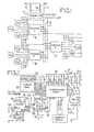
- Figure 1 is an overall block diagram of the road vehicle electrical system,
- Figure 2 is a block diagram of a transmitter which forms part of the system of Figure 1,
- Figure 2a is a graph illustrating the outputs from the transmitter of Figure 2,
- Figure 3 is a block diagram of a receiver which forms part of the system of Figure 1,
- Figures 4, 5 and 6 are circuit diagrams showing portions of the receiver of Figure 3,
- Figure 7 is a circuit diagram showing one load circuit of the receiver of Figure 3.
- Referring firstly to Figure 1, the system described includes a
transmitter 10, which has inputs controlled by a plurality of driver operable switches S1 to S8 inclusive, which are required to control various vehicle functions such as, for example, the vehicle parking lights, the main beam headlamp, the dipped headlamps, right and left direction indicator lamps, a fog lamp, reversing lamps and brake lamps respectively. Instead of the conventional arrangement utilising separate lamp-current carrying wires connecting these switches directly to the lamps controlled thereby there is a single current carryingconductor 12 connected to all the loads which are controlled byreceivers - The
transmitter 10 is connected to the receivers only by a pair ofconductors - In Figure 2 the
transmitter 10 is shown to include a microprocessor basedcircuit 20, the details of the internal connections and programming whereof are not given, but which will be understood by one skilled in the art as a result of the following description of the output signals obtained. - Each of the switches S1 to S8 controls the connection of an input port of the
circuit 20 to asupply rail 21 held at a regulated voltage (lower than the battery voltage). A further input port of thecircuit 20 is connected to the common-point of tworesistors 22, 23 connected in series between theDATA BUS 16 and the vehicle earth. - The
circuit 20 has two of its output ports connected to drive circuits for transmitting pulse code modulated signals to the DATA BUS l6 and CLOCKLINE 17. The drive circuit for theDATA BUS 16 includes aninput transistor 24 which has its emitter earthed and its base connected to the appropriate output port by aresistor 25 and acapacitor 26 in parallel. The collector of thetransistor 24 is connected by aresistor 27 to the base of apnp output transistor 28, the emitter of which is connected to therail 21. A resistor 29 is connected between the base and emitter oftransistor 28 to bias it off and acapacitor 30 is connected between the base and collector oftransistor 28, to limit the rate of change of the signal at such collector which is connected to theDATA BUS 16. A resistor 31 is connected between the BUS l6 and earth to provide a suitable load for thetransistor 28 and determine the time constant of thecapacitor 30. - The drive circuit for the CLOCK
LINE 17 is identical. - Further output ports of the
circuit 20 are connected to alamp array 32 to indicate which of the switches S1 to S8 have been closed and to a further display panel 33 intended to indicate faulty lamps as will hereinafter be made clear. Thelamp array 32 is merely intended to act as a reminder to the driver that certain loads are energised. - A system failure detector is included in the transmitter, which is also used for delaying start up of the transmitter at switch on and to ensure that the transmitted data sequence commences correctly.
- This failure detector includes a dual
monostable circuit 35 with one input 2B connected to an output of thecircuit 20 and the corresponding output Qp connected to one of the reset terminals of adecade counter 36. Thecounter 36 has its QD output connected to one of its input terminals A IN the other of which BD IN is connected to the output of an astable multi-vibrator circuit based on a well-known 555 type integratedcircuit 37. The QA and QD outputs of thecounter 36 are connected to the inputs of aNAND gate 38, the output of which is connected to the 1B input of the dualmonostable circuit 35. The Q1 output of the dual monostable circuit is connected via aninverter circuit 39 to a reset terminal of themicroprocessor circuit 20. - The
counter 36 operates as a divide-by-ten counter providing falling edge input to the dualmonostable circuit 35 so that the microprocessor is reset viainverter 39 if the QA and QD outputs ofcounter 36 ever output 1 simultaneously. This is normally prevented from happening by the provision of an output pulse from themicroprocessor circuit 20 once per page which causes one of the monostable circuits ofcircuit 35 to produce a 1 microsecond reset pulse which resetcounter 36 once per page and prevents it counting up to nine. During start up the microprocessor circuit is reset when thecounter 36 has received ten pulses from theastable multivibrator 37 whereafter the normal cycle commences. - Each of the receivers is assigned an address code, which in the present example is a five bit digital code. This allows up to 25-1 (i-e.31) receivers to be employed. Each receiver in the present example controls five separate loads so that a five bit command code is required to control each group of loads. In addition, each receiver is arranged to generate a five bit reply code indicating the current state (on or off) of its five loads.
- The transmitter is required to produce a sequence of pulse coded words containing the address codes and command codes. The transmitter, is also required to produce clock signals on the CLOCK
LINE 17,.synchronised with the bits of each coded word. Figure 2a shows the CLOCK LINE signals and the signals on theDATA BUS 16 in one cycle of operation of the transmitter and the effect of changing one of the switches S to S8 on the signals onDATA BUS 16. - The top wave form in Figure 2a shows the clock signals which are transmitted during the time when one word is transmitted on the
DATA BUS 16. As shown before the word commences the signal on the CLOCKLINE 17 is low and immediately before commencement of transmission of the word, the signal on the CLOCK LINE goes high for three clock periods and then goes low and high for alternate clock periods until it has gone high fifty times. The clock line signal then remains low for a time until transmission of the next word is about to commence. - The second wave form shown in Figure 2a shows the coded signal associated with the receiver coded 10001. As will be seen the first 1 in the address code commences as the triple length clock pulse ends and lasts two clock periods. There is then a gap of fourteen clock periods when the DATA BUS signal goes high again for two clock periods. The DATA has signal then goes low again for two clock periods and the address code is then transmitted again. The command code is then transmitted in this case merely a single pulse denoting a command code 10000. Thereafter the inverse of the command code - i.e. Ollll is transmitted. Finally a reply code 10000 is produced by the receiver, indicating that the loads controlled by that receiver are appropriately energised.
- The final waveform shown in Figure2a contains the same address code and address repeat code, but the command code is 11000 and the inverse command code 00111. The reply code is 11000.
- In the case for example, when the address code 10001 indicates a receiver at the left hand front corner of the vehicle the five loads controlled by the receiver may be the left side-light, the left main beam headlamp filament the left dip beam filament, the left front direction indicator and a fog lamp. During the production of the middle waveform of Figure 2 only the side light switch S1 was closed, but in the lower waveform the change has arisen because the switch S2 for the main beam headlamps has been closed. It will be appreciated that in the first case corresponding signals will go to the receivers at all four corners of the vehicle, whereas the added signals in the second case will go only to the front corner receivers.
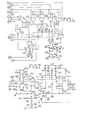
- The receiver shown in Figure 3 includes an
input shift register 50 loading of which is controlled by a control logic circuit 51 receiving an input signal from theCLOCK LINE 17. The receiver includes asecond register 52 and athird register 53 which actually provides output signals to drivecircuits 54 controlling the loads. Eachregister - Firstly, when a triple length clock signal is received by the logic circuit 31 the first five bits of the word are clocked into the
register 50. These five bits are transferred into theregister 52 by the action of the circuit 51 and the next five bits of the word are then admitted to theregister 50. - Following clocking in of the second five bits of the word a
verification logic circuit 56 checks that the contents ofregisters register 50 and transferred to theregister 52 and the fourth five bits are clocked intoregister 50, Theverification logic circuit 56 now checks whether the two command codes are mutually inverse and if not closes dawn the receiver. If the two command codes are mutually inverse, the contents ofregister 52 are transferred intoregister 53 to cause any necessary changes in the load states. - At this stage the signals on five output terminals from the
drive circuits 54 representing the actual states of the loads are transferred into theregister 50 and then clocked out on to theDATA BUS 16 via anoutput gate 57 controlled by the logic circuit 51. - Figure 3 also shows a
failsafe circuit 58 which is controlled by theverification circuit 56. If thecircuit 56 fails to produce a command code verified signal within a predetermined time interval (greater two complete cycles of the transmitter) thecircuit 58 produces an output to drive the drive circuits into a selected "safe" condition. - As shown in Figure 4, the
register 50 consists of twoMC 14035shift register circuits 50a, 50b connected in cascade, three stages of thecircuit 50b being unused. The CLOCK terminal of eachcircuit 50a, 50b is connected to a terminal A (Figure 5) and the PARALLEL/SERIAL terminal of each is connected to the output of aninverter 60 having its input connected to a terminal B (Figure 5). The J and K input terminals of the circuit 50a are connected to theDATA BUS 16 via a resistor 61, clipping diodes being connected to prevent damage to the circuit 50a. The J and K input terminals ofcircuit 50b are connected to the Q3 output of the circuit 50a. The RESET terminals ofcircuits 50a and 50b are connected to a terminal C(Figure 5). - The
register 52 consists of two four bit latch circuits type MC 14042 marked 52a and 52b. The D0, D1, D2 and D3 data input terminals of circuits 52a are connected to corresponding ones of the Q0, Q1, Q2 and Q3 outputs of the circuits 50a and the D0 input ofcircuit 52b is connected to the Q0 output ofcircuit 50b. The CLOCK inputs ofcircuits 52a and 52b are connected to the output of a NORgate 62 having one input connected to the output of aNAND gate 63 and its other input connected to a terminal D (Figure 6). Thegate 63 has an input from terminal C, and inputs from two terminals E and F (Figure 5). - The
register 53 consists of two further MC 14042latch circuits 53a and 53b. The D0 to D3 data inputs of circuit 53a are connected to the Q0 to Q3 outputs of circuit 52a and the D0 input ofcircuit 53b is connected to the Q0 output ofcircuit 52b. The CLOCK inputs ofcircuits 53a and 53b are connected to the output of a NORgate 64 with one input from the output ofNAND gate 63, one input from aNAND gate 65 and one input from a terminal G, (Figure 6). - The address recognition logic includes five EXCLUSIVE OR gates 66, 67, 68, 69 and 70 each of which has one terminal connected to an appropriate one of the Q output terminals of the
circuits 50a, 50b. The other terminal of each gate 66, to 70 is connected either to a supply rail or to earth to define the address code of the receiver in question. These other terminals are left-open in Figure 4. The outputs of the gates 66 to 70 are connected to the inputs of a NORgate 71, the output of which is connected to one input of a NAND gate 72, the output of which is connected to a terminal H (Figure 6). - The
verification logic 56 includes five EXCLUSIVE ORgates circuits 50a, 50b and its other input connected to the corresponding one of the Q outputs of thecircuits 52a, 52b. The outputs ofgates 73 to 77 are connected to the inputs of another NORgate 78, the output of which is connected to the other input of NAND gate 72. - The
NAND gate 65 has its inputs connected to the outputs ofgates 73 to 77. - It will be appreciated that gates 66 to 70 and 73 to 77 each produces a low output when the inputs to its input terminals are the same. Thus if the Q outputs of
circuits 50a and 50b match the receiver address codes there will be a low output from all of the gates 66 to 70 and hence the output of the NORgate 71 will be high. If any bit of the address differs from the corresponding Q output ofcircuit 50a or 50b the output of that gate will be high so that the output ofgate 71 will be low enabling the output of gate 72 to go high. This latter condition holds if any Q output ofcircuits 50a, 50b differs from the corresponding Q output ofcircuits 52a, 52b. The output ofgate 65 is low only when the Q outputs ofcircuits 52a, 52b are the inverse of the Q outputs ofcircuits 50a, 50b. The output terminal of thegate 63 is connected to a terminal J (Figure 6) and the Q0 output ofcircuit 50b is connected to a terminal K (Figure 6). - The failsafe circuit includes an inverter so which has its input connected by a
capacitor 81 to the output ofgate 64 and by aresistor 82 to the Ydd line of the receiver (each receiver including its own power supply stabiliser- not shown). The output ofinverter 80 is connected to the anode of adiode 83, the cathode of which is connected to the input of anotherinverter 84. Thisinverter 84 input is also connected by aresistor 85 andcapacitor 86 in parallel to earth. Finally athird inverter 87 has its input connected to the output ofinverter 84 and its output connected to a FAILSAFE terminal (Figure 7). - The output of
gate 64 goes from low to high only when the output ofgate 65 goes low whilst the output ofgate 63 is low and the signal at terminal G is low and this transition indicates verification of a command code. It is this transition which causes thecircuits 53a, 53b to be refreshed from the corresponding Q outputs ofcircuits 52a, and 52b. This transition also causes the input ofinverter 80 to go low, thereby causing thecapacitor 86 to be charged up viadiode 83, thereby maintaining the signal at the FAILSAFE terminal high. Thecapacitor 86 discharges via the resistor and if it is not re-charged periodically its voltage will fall so low that the FAILSAFE output goes low, the effect of which will be explained hereinafter. - Figure 5 shows part of the control logic 51, and includes a part of the control logic which is intended to recognise the triple length clock pulse which occurs at the commencement of each word. To this end there is provided a
local oscillator 90 consisting of two NORgates resistor 93 and acapacitor 94. Theresistor 93 is connected between the input andoutput gate 91, the output ofgate 91 being connected to the input ofgate 92, and thecapacitor 94 is connected between the output ofgate 92 and the input ofgate 91. - The output of the
gate 92 is applied to the CLOCK terminals of two four-bit shift registers 95, 96 together making up a type MC 14015 integrated circuit. The DATA input of theregister 95 and the RESET input of theregister 96 are connected to theCLOCK LINE 17 via aresistor 97, clipping diodes again being provided for protection of the integrated circuits. Twoinverters CLOCK LINE 17 to RESET input ofregister 95 and the DATA input of theregister 96 respectively, the output ofinverter 99 being connected to the terminal E. The Q3 outputs of theregisters flop circuit 100 the D and CLOCK inputs of which are both grounded. The Q output of flip-flop circuit 100 is connected to one input of aNAND gate 101 having its other input connected to a terminal L (Figure 6). The Q output ofregister 96 is also connected to a terminal M (Figure 6). - The output terminal of the
NAND gate 101 is connected to terminal C and provides reset signals for the receiver logic. The shift registers 95 and 96 are clocked by thelocal oscillator 90. Between data words, while the CLOCK LINE signal is low, the signal at the DATA input of register 15 is high and the output from the Q3 output of this register therefore runs high, maintaining the flip-flop 100 in its RESET condition, i.e. with its Q output low. Provided the signal at terminal L is also low, the output ofgate 101 is high. When the triple length pulse appears on theCLOCK LINE 17 at the commencement of a data word, register 96 is reset, but this high signal is clocked throughregister 95 so as to set flip-flop 101 and cause the output ofgate 101 to go low. The frequency ofoscillator 90 is arranged to be sufficient to ensure that the CLOCK LINE high is clocked through before the first data pulse commences. - The CLOCK LINE signal is also applied to the CLOCK input of a D type flip-
flop circuit 102 which forms the first stage of a control counter for the receiver. The RESET terminal ofcircuit 102 is connected to the output ofgate 101. The D input terminal ofcircuit 102 is connected to a terminal N (Figure 6). The Q output ofcircuit 102 is connected to terminal A and the Q output is connected to terminal N. Thecircuit 102 operates as a divide-by-two input stage, providing out of phase pulse trains at half the clock frequency at terminals A and N whenever the output ofgate 101 is low. - The second stage of the control counter is a J/K type flip-
flop circuit 103, followed by a J/K flip-flop circuit 104 and a D type flip-flop circuit 105 connected with a NORgate 106 as a divide-by-five counter. The CLOCK inputs ofcircuits Q output ofcircuit 102, their RESET terminals are all connected to the output ofgate 101, and their SET terminals are all earthed. The J and K input terminals ofcircuit 103 are connected to the Q output terminal ofcircuit 105. The J and K input terminals ofcircuit 104 are connected to the Q output ofcircuit 103. The D input ofcircuit 105 is connected to the output ofgate 106 which has one input from the Q output ofcircuit 103 and its other input from the Q output ofcircuit 104. The Q output ofcircuit 105 is connected to terminal F and its Q output is connected to a terminal P (Figure 6). - The control counter also includes two further J/K type flip-
flop circuits gate 110 as a further divide-by-five counter. The CLOCK inputs ofcircuits circuit 105, their RESET terminals are all connected to the output ofgate 101 and their SET terminals are all connected to earth. The J and K inputs ofcircuit 107 are connected to the Q output ofcircuit 109 which is also connected to a terminal Q (Figure 6). The J and K inputs ofcircuit 108 are connected to the Q output ofcircuit 107 and the D input ofcircuit 109 is connected to the output ofgate 110 which has one input from the Q output ofcircuit 108 and its other input from the Q output ofcircuit 107. The Q and Q outputs ofcircuit 107, the Q and Q outputs ofcircuit 108, and the Q output ofcircuit 109 are connected respectively to terminals R,S,T,U and V (all Figure 6). - A NAND gate 111, which has inputs from the Q output of
circuit 104, the Q output ofcircuit 105 and the Q output ofcircuit 109 has its output terminal connected to terminal B. - Turning now to Figure 6, the remainder of the control logic is shown therein. A NOR
gate 120 has two of its input terminals connected to terminals H and J respectively and a third input terminal connected to the output of aninverter 121. The output ofgate 120 is connected to the CLOCK terminal of a D type flip flop circuit 122, the SET input terminal of which is earthed and the RESET input terminal of which is connected to terminal M. The D input of circuit 122 is connected to the output of a NORgate 123 which has two inputs from terminals N and P respectively and a third input from the output ofinverter 121. - The input to
inverter 121 is connected to the output of a NORgate 124 having inputs from terminals S, T and V respectively. A further NORgate 125 has inputs from terminals R, T and V respectively. A NORgate 126 has inputs from the Q output of circuit 122 and from the outputs ofgates gate 126 is connected to the input of aninverter 127 which has its output connected to terminal L. A NORgate 128 has inputs from terminals R, U and V respectively and its output is connected to one input of a NORgate 129 which has its other input connected to the output of thegate 125. The output ofgate 129 is connected to terminal C. - A
NAND gate 130 has inputs from terminals Q, R and T respectively and its output is connected to terminal G. Afurther NAND gate 131 has inputs from terminals A, K and V respectively and from the Q output of circuit 122. The output ofgate 131 is connected to the input of aninverter 132, the output of which is connected by acapacitor 133 to earth and by aresistor 134 andcapacitor 135 in parallel to the base of annpn transistor 136. The emitter oftransistor 136 is earthed and its collector is connected by aresistor 137 to the base of a pnp transistor 138 which is biased off by a resistor 139 connected between the base and emitter thereof. The emitter of transistor 138 is connected to the receiver Vdd rail and its collector is connected to theDATA BUS 17. - As mentioned above, at the beginning of the transmission of a data word the CLOCK LINE signal goes high and this high signal is clocked through the
register 95 and removes the reset signal at the output ofgate 101. - The data bits are presented at the J and K inputs of register 50a and this data is clocked into the
registers 50a and 50b by the rising edges of the pulses at the CLOCK inputs of theregisters 50a and 50b. These pulses are derived from the Q output ofcircuit 102 and their rising edges occur at the centre of each data bit. After five such edges have been produced theregisters 50a and 50b contain the address code. This code is loaded into thecircuits 52a and 52b as a result of a clock signal which is gated bygate 63 when the Q output ofcircuit 105 goes high. - Data continues to be clock into the
registers 30a and 50b for another five pulses and the address recognition circuits then come into effect. Thus the output of gate 72 now goes low causing circuit 122 to be set only if the address code inregister 50a and 50b is the same as that incircuits 52a and 52b and the same as that preset for the receiver in question. If this does not occur the output ofgate 126 goes high causing the output ofgate 101 to reset the circuits and prevent further input. - Data input to the
registers 50a and 50b now continues so that the command code is clocked into these registers. Once again, at the end of this period, thecircuits 52a and 52b are loaded with data from theregisters 50a and 50b and clocking in of the inverse command code proceeds; At the end of thisperiod gates 73 to 77 compare the two codes andgate 65 output goes low if the two codes are inverse. This signal is gated bygate 64 with the signal fromgate 63 and that fromgate 130 to produce a clock signal for loading the contents ofcircuits 52a and 52b intocircuits 53a and 53b. If no pulse appears atgate 64 for a number oftransmitter cycles capacitor 86 discharges as explained above the output ofinverter 87 goes low. - At this stage the output of gate 111 goes low for a time so that the load data is loaded into the
registers 50a and 50b. Clocking of these registers continues so that the respective bits of the load data are outputted serially at terminal K and gated onto theDATA BUS 17 viagate 131. - Turning now to Figure 7 one load drive circuit is shown. The
input terminal 150 is connected to an appropriate one of the Q output terminals of thecircuits 53a 53b of the appropriate receiver. -
Terminal 150 is connected by acapacitor 151 and aresistor 152 in series to the baseof annpn transistor 153, the emitter of which is connected to earth, aresistor 154 connecting the base oftransistor 153 to earth to bias it off. The collector oftransistor 153 is connected by tworesistors pnp transistor 157 which has its emitter connected to the Vdd rail. The collector of thetransistor 157 is connected to the anode of adiode 153, the cathode of which is connected by aresistor 159 to the base of a npn transistor 160 and by aresistor 161 to the collector of an npn transistor 162. The emitters of both these transistors 160, 162 arc earthed and aresistor 163 connects the base of transistor 162 to earth. The collector of transistor l60 is connected to the base of transistor 162. - The collector of
transistor 164 is connected to the base of annpn transistor 164, the emitter of which is connected to the base of annpn transistor 165 which has its emitter earthed. The collectors oftransistors battery rail 12, a freewheel diode 167 being connected across this winding. - The relay has a normally open contact 168 which connects one end of a
series resistor 169 to therail 12. The other end of theresistor 169 is connected to earth by the load. Said one end ofresistor 169 is connected to the anodes of twodiodes 170 and 171. The cathode ofdiode 170 is connected by tworesistors resistors pnp transistor 176 has its base connected to the junction ofresistors resistor 169 and its collector connected by aresistor 177 to the base of transistor 162. Afurther pnp transistor 178 has its base connected to the junction ofresistors resistors 169 and its collector connected by aresistor 179 to the cathode ofdiode 158. -
A-diode 180 connects the collector of transistor 162 to theinput terminal 150. - When it is required to switch on a load the signal at
terminal 150 goes high. This causestransistors capacitor 151 is charging. During this time current flowing throughresistor 161 causes thetransistors resistor 161 preventstransistor 178 having any effect and current throughresistor 159 turns on transistor 160 and preventstransistor 176 having any effect. - At the end of this initial time period, the
transistor 178, which turns on if the load current is normal holds the transistor l64, 165 on, thereby latching the relay in the .on condition. - If there is a fault such that an abnormally high current flows in the load,
transistor 178 turns off because the voltage at its emitter falls lower than that required for the emitter base junction to conduct. As aresult transistor - If there is a fault such that an abnormally low or no current flows in the load the
transistor 176 turns on (because the voltage drop acrossresistor 169 is reduced to zero in an open circuit condition). This causes transistor 162 to turn on, thereby turning off transistors l64 and 165 and de-energising the relay. - When the signal at
terminal 150 is low thetransistors diode 180. Thecapacitor 151 discharges. - The FAILSAFE terminal (Figure 4) is connected to the base of a
pnp transistor 190 which has its emitter connected to the Vdd rail. The collector oftransistor 190 is connec- .ted by tworesistors npn transistor 193 which has its emitter earthed. The collector oftransistor 193 is connected either by adiode 194 to the base oftransistor 164 or by adiode 195 to the collector oftransistor 165, depending on whether it is required for the particular load to be turned off or on in the failsafe mode.
Claims (6)
Applications Claiming Priority (2)
| Application Number | Priority Date | Filing Date | Title |
|---|---|---|---|
| GB7849766 | 1978-12-22 | ||
| GB4976678 | 1978-12-22 |
Publications (2)
| Publication Number | Publication Date |
|---|---|
| EP0013103A1 true EP0013103A1 (en) | 1980-07-09 |
| EP0013103B1 EP0013103B1 (en) | 1983-06-29 |
Family
ID=10501903
Family Applications (1)
| Application Number | Title | Priority Date | Filing Date |
|---|---|---|---|
| EP79302895A Expired EP0013103B1 (en) | 1978-12-22 | 1979-12-14 | Motor vehicle electrical system |
Country Status (11)
| Country | Link |
|---|---|
| US (1) | US4302841A (en) |
| EP (1) | EP0013103B1 (en) |
| JP (1) | JPS55105490A (en) |
| AU (1) | AU537369B2 (en) |
| BR (1) | BR7908472A (en) |
| DE (1) | DE2965810D1 (en) |
| ES (1) | ES487134A1 (en) |
| IN (1) | IN150897B (en) |
| PL (1) | PL128215B1 (en) |
| YU (1) | YU314779A (en) |
| ZA (1) | ZA796811B (en) |
Cited By (9)
| Publication number | Priority date | Publication date | Assignee | Title |
|---|---|---|---|---|
| FR2519815A1 (en) * | 1982-01-13 | 1983-07-18 | Aerospatiale | Aircraft electricity distribution system - includes relay switches linking bus=bars to alternator supplies with flip=flops signalling switch states |
| USRE31582E (en) * | 1979-03-23 | 1984-05-08 | Nissan Motor Company, Limited | Automatic control system for method and apparatus for checking devices of an automotive vehicle in use with a microcomputer |
| EP0153434A1 (en) * | 1983-02-23 | 1985-09-04 | Petri AG | Electric vehicle control device |
| GB2189335A (en) * | 1986-04-19 | 1987-10-21 | Edward Dorian Bailey | Electric signalling system |
| GB2223913A (en) * | 1988-10-15 | 1990-04-18 | Electronic Components Ltd | Data communication system |
| EP0396089A2 (en) * | 1989-05-04 | 1990-11-07 | STMicroelectronics S.r.l. | Connection system between a master and slave processing units |
| EP0422507A2 (en) * | 1989-10-09 | 1991-04-17 | Nissan Motor Co., Ltd. | System and method for communicating data between control unit and master station applicable to automotive vehicle |
| GB2266392A (en) * | 1992-04-16 | 1993-10-27 | Equus Inc | A three-line type of vehicle burglarproof system. |
| FR2713164A1 (en) * | 1993-12-02 | 1995-06-09 | Daimler Benz Ag | Lighting control device for a motor vehicle. |
Families Citing this family (14)
| Publication number | Priority date | Publication date | Assignee | Title |
|---|---|---|---|---|
| JPS57155601A (en) * | 1981-03-20 | 1982-09-25 | Nippon Denso Co Ltd | Car safety device |
| DE3149142A1 (en) * | 1981-12-11 | 1983-06-23 | Wabco Westinghouse Fahrzeugbremsen GmbH, 3000 Hannover | MULTIPLEX WIRING SYSTEM FOR VEHICLES |
| JPS59117395A (en) * | 1982-12-24 | 1984-07-06 | Hitachi Ltd | Terminal processing device |
| JPS6229247A (en) * | 1985-07-29 | 1987-02-07 | Nippon Soken Inc | On-vehicle local area network |
| JPH01137853A (en) * | 1987-11-25 | 1989-05-30 | Toshiba Corp | Communication control system |
| US4839530A (en) * | 1988-01-07 | 1989-06-13 | Salplex Limited | Information handling and control systems |
| US4956561A (en) * | 1988-12-27 | 1990-09-11 | Caterpillar Inc. | Smart power connector |
| JP2791169B2 (en) * | 1990-03-08 | 1998-08-27 | 株式会社日立製作所 | Centralized wiring system for automobiles |
| FR2662736B1 (en) * | 1990-06-05 | 1992-10-30 | Rockwell Abs France | DEVICE FOR CENTRALIZED CONTROL OF OPENING ELEMENTS OF A MOTOR VEHICLE. |
| NL9401923A (en) * | 1994-11-17 | 1996-07-01 | Gti Holding Nv | Method and device for processing signals in a safety system. |
| US5907195A (en) * | 1997-05-30 | 1999-05-25 | Directed Electronics, Inc. | Channel expander for remotely controlled automotive security and convenience systems |
| US6800957B2 (en) * | 2001-02-06 | 2004-10-05 | General Electric Company | Electronic distribution system for 36V automobiles |
| US20030176951A1 (en) * | 2002-01-09 | 2003-09-18 | Demarchi Julian A. | System integrating a reformer and a fuel cell system |
| US9573619B2 (en) * | 2012-10-10 | 2017-02-21 | Nsk Ltd. | Physical quantity detecting device and electric power steering apparatus using same |
Citations (7)
| Publication number | Priority date | Publication date | Assignee | Title |
|---|---|---|---|---|
| DE1043384B (en) * | 1951-01-20 | 1958-11-13 | Siemens Ag | Method and circuit arrangement for transmitting telegraphic messages which are secured by a security group added to the step group |
| DE1135949B (en) * | 1960-06-01 | 1962-09-06 | Siemens Ag | Method for the partially secure transmission of telegraphic characters, in which each telegraphic character to be transmitted is composed of two partial characters with six steps each |
| DE1194442B (en) * | 1964-07-03 | 1965-06-10 | Siemens Ag | Method and device for interference-proof transmission of binary signals |
| GB1494240A (en) * | 1974-07-10 | 1977-12-07 | Bosch Gmbh Robert | Vehicle electrical switching operation control apparatus |
| DE2658521A1 (en) * | 1976-12-23 | 1978-06-29 | Siemens Ag | CIRCUIT ARRANGEMENT FOR SECURELY REQUESTING THE SWITCH POSITIONS OF SWITCHES, IN PARTICULAR NUMBER ADJUSTERS |
| US4130241A (en) * | 1976-03-10 | 1978-12-19 | Smiths Industries Limited | Control systems |
| EP0000427A1 (en) * | 1977-07-09 | 1979-01-24 | LUCAS INDUSTRIES public limited company | Road vehicle electrical systems |
Family Cites Families (8)
| Publication number | Priority date | Publication date | Assignee | Title |
|---|---|---|---|---|
| US3624603A (en) * | 1969-09-16 | 1971-11-30 | Gen Electric | Digital data communications system with means for improving system security |
| US3876980A (en) * | 1973-11-05 | 1975-04-08 | Products Of Information Techno | Vehicle location systems |
| US3906445A (en) * | 1974-10-21 | 1975-09-16 | Motorola Inc | Alphanumeric terminal for a communications system |
| AT335005B (en) * | 1975-01-22 | 1977-02-25 | Leinfellner Helmut Ing | ERROR DETECTING TRANSMISSION SYSTEM FOR INFORMATION BY MEANS OF PULSE TRAINS OF A SPECIFIED LENGTH |
| US3973242A (en) * | 1975-02-27 | 1976-08-03 | Gte Sylvania Incorporated | Digital receiver |
| IT1061720B (en) * | 1976-06-04 | 1983-04-30 | Fiat Spa | ELECTRIC SYSTEM FOR THE DISTRIBUTION OF ENERGY PARTICULARLY FOR VEHICLES |
| DE2640756C2 (en) * | 1976-09-10 | 1982-11-04 | Standard Elektrik Lorenz Ag, 7000 Stuttgart | Device for secure data transmission in track-bound vehicles |
| US4156866A (en) * | 1976-10-07 | 1979-05-29 | Systems Technology Corporation | Multiple remote terminal digital control system |
-
1979
- 1979-12-14 DE DE7979302895T patent/DE2965810D1/en not_active Expired
- 1979-12-14 ZA ZA00796811A patent/ZA796811B/en unknown
- 1979-12-14 EP EP79302895A patent/EP0013103B1/en not_active Expired
- 1979-12-17 AU AU53886/79A patent/AU537369B2/en not_active Ceased
- 1979-12-18 US US06/105,045 patent/US4302841A/en not_active Expired - Lifetime
- 1979-12-20 ES ES487134A patent/ES487134A1/en not_active Expired
- 1979-12-21 BR BR7908472A patent/BR7908472A/en unknown
- 1979-12-21 YU YU03147/79A patent/YU314779A/en unknown
- 1979-12-22 PL PL1979220700A patent/PL128215B1/en unknown
- 1979-12-22 IN IN1336/CAL/79A patent/IN150897B/en unknown
- 1979-12-22 JP JP16743779A patent/JPS55105490A/en active Pending
Patent Citations (7)
| Publication number | Priority date | Publication date | Assignee | Title |
|---|---|---|---|---|
| DE1043384B (en) * | 1951-01-20 | 1958-11-13 | Siemens Ag | Method and circuit arrangement for transmitting telegraphic messages which are secured by a security group added to the step group |
| DE1135949B (en) * | 1960-06-01 | 1962-09-06 | Siemens Ag | Method for the partially secure transmission of telegraphic characters, in which each telegraphic character to be transmitted is composed of two partial characters with six steps each |
| DE1194442B (en) * | 1964-07-03 | 1965-06-10 | Siemens Ag | Method and device for interference-proof transmission of binary signals |
| GB1494240A (en) * | 1974-07-10 | 1977-12-07 | Bosch Gmbh Robert | Vehicle electrical switching operation control apparatus |
| US4130241A (en) * | 1976-03-10 | 1978-12-19 | Smiths Industries Limited | Control systems |
| DE2658521A1 (en) * | 1976-12-23 | 1978-06-29 | Siemens Ag | CIRCUIT ARRANGEMENT FOR SECURELY REQUESTING THE SWITCH POSITIONS OF SWITCHES, IN PARTICULAR NUMBER ADJUSTERS |
| EP0000427A1 (en) * | 1977-07-09 | 1979-01-24 | LUCAS INDUSTRIES public limited company | Road vehicle electrical systems |
Cited By (13)
| Publication number | Priority date | Publication date | Assignee | Title |
|---|---|---|---|---|
| USRE31582E (en) * | 1979-03-23 | 1984-05-08 | Nissan Motor Company, Limited | Automatic control system for method and apparatus for checking devices of an automotive vehicle in use with a microcomputer |
| FR2519815A1 (en) * | 1982-01-13 | 1983-07-18 | Aerospatiale | Aircraft electricity distribution system - includes relay switches linking bus=bars to alternator supplies with flip=flops signalling switch states |
| EP0153434A1 (en) * | 1983-02-23 | 1985-09-04 | Petri AG | Electric vehicle control device |
| GB2189335A (en) * | 1986-04-19 | 1987-10-21 | Edward Dorian Bailey | Electric signalling system |
| GB2223913A (en) * | 1988-10-15 | 1990-04-18 | Electronic Components Ltd | Data communication system |
| EP0396089A3 (en) * | 1989-05-04 | 1992-08-26 | STMicroelectronics S.r.l. | Connection system between a master and slave processing units |
| EP0396089A2 (en) * | 1989-05-04 | 1990-11-07 | STMicroelectronics S.r.l. | Connection system between a master and slave processing units |
| US5592485A (en) * | 1989-05-04 | 1997-01-07 | Sgs-Thomson Microelectronics S.R.L. | Connection system between a master and slave processing units |
| EP0422507A2 (en) * | 1989-10-09 | 1991-04-17 | Nissan Motor Co., Ltd. | System and method for communicating data between control unit and master station applicable to automotive vehicle |
| EP0422507A3 (en) * | 1989-10-09 | 1991-09-18 | Nissan Motor Co., Ltd. | System and method for communicating data between control unit and master station applicable to automotive vehicle |
| GB2266392A (en) * | 1992-04-16 | 1993-10-27 | Equus Inc | A three-line type of vehicle burglarproof system. |
| GB2266392B (en) * | 1992-04-16 | 1995-10-11 | Equus Inc | A three-line type of vehicle burglar-detecting system |
| FR2713164A1 (en) * | 1993-12-02 | 1995-06-09 | Daimler Benz Ag | Lighting control device for a motor vehicle. |
Also Published As
| Publication number | Publication date |
|---|---|
| ZA796811B (en) | 1980-11-26 |
| ES487134A1 (en) | 1980-06-16 |
| PL220700A1 (en) | 1980-09-08 |
| EP0013103B1 (en) | 1983-06-29 |
| YU314779A (en) | 1983-02-28 |
| IN150897B (en) | 1983-01-08 |
| AU537369B2 (en) | 1984-06-21 |
| AU5388679A (en) | 1980-06-26 |
| PL128215B1 (en) | 1984-01-31 |
| BR7908472A (en) | 1980-09-23 |
| JPS55105490A (en) | 1980-08-13 |
| DE2965810D1 (en) | 1983-08-04 |
| US4302841A (en) | 1981-11-24 |
Similar Documents
| Publication | Publication Date | Title |
|---|---|---|
| US4302841A (en) | Motor vehicle electrical system | |
| US4538262A (en) | Multiplex bus system for controlling the transmission of data between a master control unit and a plurality of remotely located receiver-transmitter units | |
| US4085403A (en) | Combined on-board remote control energy supply distribution and signaling system, particularly for automotive vehicles | |
| CA1037170A (en) | Time division multiplex system for a motor vehicle | |
| US5216674A (en) | Method of and device for bringing a network interface out of a sleep mode into a wake-up state | |
| EP0102682A2 (en) | Apparatus and method for communication | |
| US4180803A (en) | Remote control system with pulse addressing, and safety warning indication | |
| US4370561A (en) | Vehicle multiplex system | |
| US4573041A (en) | Electric wiring system having a plurality of sensors | |
| US4028620A (en) | Electrical wiring system for selectively actuating electrical loads | |
| EP0011313A1 (en) | Road vehicle electrical systems | |
| US4164730A (en) | Externally controllable binary interrogation and decoding circuit, particularly for a remote control load selection system | |
| EP0023105A1 (en) | System and method for handling multiplex information | |
| US3648057A (en) | Vehicular plex-path circumferential control and distribution system | |
| US4163217A (en) | Remote load control system | |
| US3701101A (en) | Modular remote control and supervisory system switchgear | |
| CA1154500A (en) | Vital contact isolation circuit | |
| EP0143650A2 (en) | Vehicle multiplex system | |
| US3944981A (en) | Electrical wiring system | |
| US4034369A (en) | Check circuit for checking vehicle warning system | |
| US4564774A (en) | Binary logic device having input and output alternating signals | |
| KR830000477B1 (en) | Automotive electrical systems | |
| JPS5840751Y2 (en) | Power supply control device for automotive electrical components | |
| SU1336037A1 (en) | Electric wiring checking device | |
| JPH0352215Y2 (en) |
Legal Events
| Date | Code | Title | Description |
|---|---|---|---|
| PUAI | Public reference made under article 153(3) epc to a published international application that has entered the european phase |
Free format text: ORIGINAL CODE: 0009012 |
|
| AK | Designated contracting states |
Designated state(s): BE DE FR GB IT NL SE |
|
| 17P | Request for examination filed |
Effective date: 19801219 |
|
| RAP1 | Party data changed (applicant data changed or rights of an application transferred) |
Owner name: LUCAS INDUSTRIES PLC |
|
| ITF | It: translation for a ep patent filed |
Owner name: SOCIETA' ITALIANA BREVETTI S.P.A. |
|
| GRAA | (expected) grant |
Free format text: ORIGINAL CODE: 0009210 |
|
| AK | Designated contracting states |
Designated state(s): BE DE FR GB IT NL SE |
|
| PG25 | Lapsed in a contracting state [announced via postgrant information from national office to epo] |
Ref country code: SE Effective date: 19830629 |
|
| REF | Corresponds to: |
Ref document number: 2965810 Country of ref document: DE Date of ref document: 19830804 |
|
| EN | Fr: translation not filed | ||
| PLBE | No opposition filed within time limit |
Free format text: ORIGINAL CODE: 0009261 |
|
| STAA | Information on the status of an ep patent application or granted ep patent |
Free format text: STATUS: NO OPPOSITION FILED WITHIN TIME LIMIT |
|
| 26N | No opposition filed | ||
| REG | Reference to a national code |
Ref country code: FR Ref legal event code: DJ |
|
| PGFP | Annual fee paid to national office [announced via postgrant information from national office to epo] |
Ref country code: FR Payment date: 19891211 Year of fee payment: 11 |
|
| PGFP | Annual fee paid to national office [announced via postgrant information from national office to epo] |
Ref country code: BE Payment date: 19891227 Year of fee payment: 11 |
|
| ITTA | It: last paid annual fee | ||
| PGFP | Annual fee paid to national office [announced via postgrant information from national office to epo] |
Ref country code: NL Payment date: 19891231 Year of fee payment: 11 Ref country code: GB Payment date: 19891231 Year of fee payment: 11 |
|
| PGFP | Annual fee paid to national office [announced via postgrant information from national office to epo] |
Ref country code: DE Payment date: 19900131 Year of fee payment: 11 |
|
| PG25 | Lapsed in a contracting state [announced via postgrant information from national office to epo] |
Ref country code: GB Effective date: 19901214 |
|
| PG25 | Lapsed in a contracting state [announced via postgrant information from national office to epo] |
Ref country code: BE Effective date: 19901231 |
|
| BERE | Be: lapsed |
Owner name: LUCAS INDUSTRIES PUBLIC LTD CY Effective date: 19901231 |
|
| PG25 | Lapsed in a contracting state [announced via postgrant information from national office to epo] |
Ref country code: NL Effective date: 19910701 |
|
| GBPC | Gb: european patent ceased through non-payment of renewal fee | ||
| NLV4 | Nl: lapsed or anulled due to non-payment of the annual fee | ||
| PG25 | Lapsed in a contracting state [announced via postgrant information from national office to epo] |
Ref country code: DE Effective date: 19910903 |
|
| PG25 | Lapsed in a contracting state [announced via postgrant information from national office to epo] |
Ref country code: FR Free format text: LAPSE BECAUSE OF NON-PAYMENT OF DUE FEES Effective date: 19901231 |