EP0012863B1 - Method of making semiconductor devices with reduced parasitic capacitance - Google Patents
Method of making semiconductor devices with reduced parasitic capacitance Download PDFInfo
- Publication number
- EP0012863B1 EP0012863B1 EP79104724A EP79104724A EP0012863B1 EP 0012863 B1 EP0012863 B1 EP 0012863B1 EP 79104724 A EP79104724 A EP 79104724A EP 79104724 A EP79104724 A EP 79104724A EP 0012863 B1 EP0012863 B1 EP 0012863B1
- Authority
- EP
- European Patent Office
- Prior art keywords
- layer
- region
- conductive layer
- substrate
- doping region
- Prior art date
- Legal status (The legal status is an assumption and is not a legal conclusion. Google has not performed a legal analysis and makes no representation as to the accuracy of the status listed.)
- Expired
Links
Images

Classifications
-
- H—ELECTRICITY
- H01—ELECTRIC ELEMENTS
- H01L—SEMICONDUCTOR DEVICES NOT COVERED BY CLASS H10
- H01L21/00—Processes or apparatus adapted for the manufacture or treatment of semiconductor or solid state devices or of parts thereof
- H01L21/02—Manufacture or treatment of semiconductor devices or of parts thereof
- H01L21/04—Manufacture or treatment of semiconductor devices or of parts thereof the devices having at least one potential-jump barrier or surface barrier, e.g. PN junction, depletion layer or carrier concentration layer
- H01L21/18—Manufacture or treatment of semiconductor devices or of parts thereof the devices having at least one potential-jump barrier or surface barrier, e.g. PN junction, depletion layer or carrier concentration layer the devices having semiconductor bodies comprising elements of Group IV of the Periodic System or AIIIBV compounds with or without impurities, e.g. doping materials
- H01L21/30—Treatment of semiconductor bodies using processes or apparatus not provided for in groups H01L21/20 - H01L21/26
- H01L21/31—Treatment of semiconductor bodies using processes or apparatus not provided for in groups H01L21/20 - H01L21/26 to form insulating layers thereon, e.g. for masking or by using photolithographic techniques; After treatment of these layers; Selection of materials for these layers
- H01L21/3105—After-treatment
- H01L21/31051—Planarisation of the insulating layers
- H01L21/31053—Planarisation of the insulating layers involving a dielectric removal step
- H01L21/31055—Planarisation of the insulating layers involving a dielectric removal step the removal being a chemical etching step, e.g. dry etching
-
- H—ELECTRICITY
- H01—ELECTRIC ELEMENTS
- H01L—SEMICONDUCTOR DEVICES NOT COVERED BY CLASS H10
- H01L21/00—Processes or apparatus adapted for the manufacture or treatment of semiconductor or solid state devices or of parts thereof
- H01L21/02—Manufacture or treatment of semiconductor devices or of parts thereof
- H01L21/04—Manufacture or treatment of semiconductor devices or of parts thereof the devices having at least one potential-jump barrier or surface barrier, e.g. PN junction, depletion layer or carrier concentration layer
- H01L21/18—Manufacture or treatment of semiconductor devices or of parts thereof the devices having at least one potential-jump barrier or surface barrier, e.g. PN junction, depletion layer or carrier concentration layer the devices having semiconductor bodies comprising elements of Group IV of the Periodic System or AIIIBV compounds with or without impurities, e.g. doping materials
- H01L21/30—Treatment of semiconductor bodies using processes or apparatus not provided for in groups H01L21/20 - H01L21/26
- H01L21/31—Treatment of semiconductor bodies using processes or apparatus not provided for in groups H01L21/20 - H01L21/26 to form insulating layers thereon, e.g. for masking or by using photolithographic techniques; After treatment of these layers; Selection of materials for these layers
- H01L21/3205—Deposition of non-insulating-, e.g. conductive- or resistive-, layers on insulating layers; After-treatment of these layers
- H01L21/321—After treatment
- H01L21/3213—Physical or chemical etching of the layers, e.g. to produce a patterned layer from a pre-deposited extensive layer
- H01L21/32133—Physical or chemical etching of the layers, e.g. to produce a patterned layer from a pre-deposited extensive layer by chemical means only
- H01L21/32134—Physical or chemical etching of the layers, e.g. to produce a patterned layer from a pre-deposited extensive layer by chemical means only by liquid etching only
-
- H—ELECTRICITY
- H01—ELECTRIC ELEMENTS
- H01L—SEMICONDUCTOR DEVICES NOT COVERED BY CLASS H10
- H01L21/00—Processes or apparatus adapted for the manufacture or treatment of semiconductor or solid state devices or of parts thereof
- H01L21/70—Manufacture or treatment of devices consisting of a plurality of solid state components formed in or on a common substrate or of parts thereof; Manufacture of integrated circuit devices or of parts thereof
- H01L21/71—Manufacture of specific parts of devices defined in group H01L21/70
- H01L21/768—Applying interconnections to be used for carrying current between separate components within a device comprising conductors and dielectrics
- H01L21/76801—Applying interconnections to be used for carrying current between separate components within a device comprising conductors and dielectrics characterised by the formation and the after-treatment of the dielectrics, e.g. smoothing
- H01L21/76829—Applying interconnections to be used for carrying current between separate components within a device comprising conductors and dielectrics characterised by the formation and the after-treatment of the dielectrics, e.g. smoothing characterised by the formation of thin functional dielectric layers, e.g. dielectric etch-stop, barrier, capping or liner layers
- H01L21/76832—Multiple layers
-
- H—ELECTRICITY
- H01—ELECTRIC ELEMENTS
- H01L—SEMICONDUCTOR DEVICES NOT COVERED BY CLASS H10
- H01L23/00—Details of semiconductor or other solid state devices
- H01L23/52—Arrangements for conducting electric current within the device in operation from one component to another, i.e. interconnections, e.g. wires, lead frames
- H01L23/522—Arrangements for conducting electric current within the device in operation from one component to another, i.e. interconnections, e.g. wires, lead frames including external interconnections consisting of a multilayer structure of conductive and insulating layers inseparably formed on the semiconductor body
- H01L23/5222—Capacitive arrangements or effects of, or between wiring layers
-
- H—ELECTRICITY
- H10—SEMICONDUCTOR DEVICES; ELECTRIC SOLID-STATE DEVICES NOT OTHERWISE PROVIDED FOR
- H10B—ELECTRONIC MEMORY DEVICES
- H10B12/00—Dynamic random access memory [DRAM] devices
- H10B12/30—DRAM devices comprising one-transistor - one-capacitor [1T-1C] memory cells
-
- H—ELECTRICITY
- H01—ELECTRIC ELEMENTS
- H01L—SEMICONDUCTOR DEVICES NOT COVERED BY CLASS H10
- H01L2924/00—Indexing scheme for arrangements or methods for connecting or disconnecting semiconductor or solid-state bodies as covered by H01L24/00
- H01L2924/0001—Technical content checked by a classifier
- H01L2924/0002—Not covered by any one of groups H01L24/00, H01L24/00 and H01L2224/00
-
- Y—GENERAL TAGGING OF NEW TECHNOLOGICAL DEVELOPMENTS; GENERAL TAGGING OF CROSS-SECTIONAL TECHNOLOGIES SPANNING OVER SEVERAL SECTIONS OF THE IPC; TECHNICAL SUBJECTS COVERED BY FORMER USPC CROSS-REFERENCE ART COLLECTIONS [XRACs] AND DIGESTS
- Y10—TECHNICAL SUBJECTS COVERED BY FORMER USPC
- Y10S—TECHNICAL SUBJECTS COVERED BY FORMER USPC CROSS-REFERENCE ART COLLECTIONS [XRACs] AND DIGESTS
- Y10S438/00—Semiconductor device manufacturing: process
- Y10S438/901—Capacitive junction
Definitions
- the invention relates to a method for producing semiconductor arrangements with reduced capacitive coupling between at least one doping region arranged in a semiconductor substrate and an electrically conductive layer provided on the substrate in isolation, which is above the doping region a greater distance from the substrate surface than outside the doping region and thus is uneven Has surface with at least one raised area.
- it relates to measures for reducing parasitic bit line capacitances in memory arrangements in which the bit lines are designed in the form of doping regions in the semiconductor substrate in question, at least one electrically conductive layer being provided over the substrate.
- US patent specification 3976524 a method for producing flat surfaces in integrated circuits, in which the surface to be leveled is first coated with a photoresist layer, which forms a photoresist pattern in the recessed areas after appropriate exposure and development in the raised areas from these and from the recessed areas marginally exposed and developed areas is removed. The unexposed photoresist pattern is then melted so that the recessed areas are completely masked. The raised areas can then be removed to the depth of the recessed areas.
- US Pat. No. 4,070,501 is also of interest, which relates to a method for the self-aligning production of multilayer pipe systems with cross connections.
- an insulation layer is applied to a substrate carrying a first line pattern, which corresponds to the surface of the topology of the line pattern, that is to say has corresponding elevations.
- a second layer is applied to the insulation layer, the thickness of which is less above the cable runs than next to them.
- the material of the second layer above the elevations is removed by means of a mask in the area of the connection holes to be formed above the cable runs.
- the connection holes in the insulation layer are formed by etching, the mask and the second layer serving as an etching mask.
- the invention achieves the object of specifying an improved production method for semiconductor arrangements with reduced parasitic capacitances, which can result from the interaction of doping regions in a substrate with conductive layers or layer regions arranged above them.
- the method should make it possible to produce capacitive single-FET memory arrangements with reduced bit line capacitance.
- the invention provides for reducing the capacitive coupling between at least one doping region arranged in a semiconductor substrate and an electrically conductive layer provided on the substrate in isolation, which is above the doping region a greater distance from the substrate surface than outside the doping region and thus an uneven surface with at least one has raised area, before to apply a relatively thick masking layer, preferably made of photoresist, to the surface of the conductive layer such that the conductive layer is completely covered with an irregular surface and a practically flat surface is formed. Then a subtractive process, e.g. an etching or development process is carried out in order to remove a uniform layer portion of the masking layer to such an extent that the raised areas of the surface of the conductive layer are exposed in some areas.
- a subtractive process e.g. an etching or development process
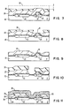
- FIG. 1 shows a semiconductor substrate 10, which is preferably made of P-conducting silicon with a specific resistance of approximately 2 to 12 ⁇ . cm.
- a layer of an arsenic-doped oxide, designated 12 is applied to the substrate 10.
- the substrate 10 was introduced into an atmosphere of gaseous silane, arsine, oxygen and nitrogen in suitable amounts for chemical precipitation by decomposition from the gas phase (CVD) in such a way that a doped oxide layer 12 of approximately 300 to 500 nm is formed, which as Diffusion source layer can serve to form PN junctions in the substrate.
- This CVD process is best carried out at around 500 ° C in an apparatus such as that e.g. in U.S. Patent 3,805,736.
- a photolithographic masking step is carried out in order to define all the regions on the surface of the substrate 10 in which diffused transitions are desired.
- the doped oxide layer 12 is then (selectively) removed in a wet etching process, for example in hydrofluoric acid buffered with ammonium fluoride.
- the regions of the doped oxide layer denoted by 14 and 16 remain on the surface of the substrate 10 in the manner shown in FIG. 2. Although a very large number of such doped regions is normally provided, only two such regions are shown in this case to describe the invention.
- the designated area 14 is in reality an extended strip which extends perpendicular to the plane and a bit - represents sense line.
- the area designated 16 is one of many areas arranged adjacent to area 14, each of which forms an isolated capacitance area.
- an uncritical (not shown) rough masking is applied, which is designed in such a way that the doped oxide layer regions can be selectively removed over such doping regions, to which a capacitively coupled covering layer of conductive material must be applied.
- a brief dip etch is performed to remove any remnant of the thermal oxide layer 18 that was previously present under the coarse masking and adjacent to the remaining oxide layer area 14, see FIG. in this respect also US Pat. No. 3,975,220.
- FIG. 4 illustrates the result following this method step.
- the oxide region denoted by 14 is maintained above the associated doping region 20 for the (diffused) bit sensing line.
- a thin thermal silicon dioxide layer 24 of about 30 nm thickness is washed in an atmosphere containing oxygen / hydrogen chloride at about 1000 ° C.
- This layer, designated 24, covers the entire exposed surface with the exception of the locations where doped oxide is present.
- This method step can also be carried out in a device of the type described in more detail in US Pat. No. 3,790,404.
- an approximately 20 nm thick silicon nitride layer 26 is applied using an atmosphere containing silane and ammonia at approximately 900 ° C.
- This is followed by the precipitation of an approximately 300 nm thick polycrystalline silicon layer 28 doped with boron from an atmosphere containing hydrogen, silane and borohydride at approximately 600 ° C.
- the latter two process steps can be carried out successively in a common process chamber of the type described in more detail in US Pat. No. 3,805,763.
- the polycrystalline silicon layer 28 is retained in some areas, namely over the doping regions 22 for the storage nodes, where it represents an electrode of the storage capacitor of the relevant memory cell, or as a shielding layer over the substrate around the doping regions 22. Layer 28 also remained over the entire length of the bit sense lines doping regions 20, which made a significant amount to increase the effective coupling capacity. This effect occurred regardless of the effective reduction in capacitive effects achieved by maintaining both the distance between the capacitor electrodes and between the doping regions 20 and the conductive layer 28 by maintaining the doped oxide regions 14.
- a relatively thick photoresist masking layer 30 is applied to the substrate.
- the layer 30 is so thick that it covers all areas of the layer designated 28 and forms an essentially flat surface according to FIG. 6.
- a conventional positive lacquer which is sold under the trade name AZ1350J by the Shipley Company, Newton, Massachusetts, can be used as the photoresist for the layer 30.
- AZ1350J is a light-sensitive polymer consisting of an m-cresol-formaldehyde novolak resin and a diazo-ketone sensitizer, dissolved in ethylene-glycol-monoethyl ether acetate.
- the photoresist may contain an additive to improve the adhesion properties, e.g.
- the photoresist can be applied using one of the conventional techniques that allow the application of so much material that an essentially flat surface can be obtained.
- the photoresist is then treated by heat treatment at 95 ° C for a time sufficient for curing.
- Consistent uniform exposure of the photoresist through a neutral density filter in order to reduce the development rate sufficiently to control the development depth L cf. e.g. U.S. Patent 3649393.
- removal by means of reactive ion etching or by means of a sputtering process can also be considered. Since a uniform photoresist layer is removed, this process step is self-adjusting and selectively exposes only the areas of the coated substrate that extend through the remaining photoresist masking layer in the manner shown in FIG.
- the then exposed polycrystalline silicon is selectively removed using a suitable etchant, e.g. by means of a solution of nitric acid, water and buffered hydrofluoric acid in a volume ratio of 7: 4: 1, the buffered hydrofluoric acid having 5 parts by volume of 40% ammonium fluoride per part by volume of 48% hydrofluoric acid.
- a suitable etchant e.g. by means of a solution of nitric acid, water and buffered hydrofluoric acid in a volume ratio of 7: 4: 1, the buffered hydrofluoric acid having 5 parts by volume of 40% ammonium fluoride per part by volume of 48% hydrofluoric acid.
- the further procedure can be carried out in the following manner in accordance with US Pat. No. 3,841,926.
- a further photolithography and etching step is used to etch the regions of the polycrystalline silicon layer 28 at which gate regions are required for the respective field effect transistors, cf. Fig. 10.
- this etching step is, however, limited to relatively small gates. Areas are limited, thereby coupling each of the numerous isolated areas 22 of the storage nodes to the elongated doping region 20 of the associated bit line.
- the actual memory cells which consist of the doping regions 20 for the bit sensing lines, the gate electrodes 38, and the storage nodes 22 and Capacitor electrodes (regions of the layer 28 above the doping regions 22) exist, are fully functional and testable.
- the electrical isolation of adjacent storage nodes 22 is possible by applying a reference potential to the polycrystalline silicon layer 28 so that the surface of the substrate 10 adjacent to the regions 20 and 22, but not under the electrodes 38 between these regions, is continuously reverse biased . This can be accomplished by applying substrate 10 and polycrystalline silicon layer 28 to a negative voltage.
Description
Die Erfindung betrifft ein Verfahren zur Herstellung von Halbleiteranordnungen mit herabgesetzter kapazitiver Kopplung zwischen mindestens einem in einem Halbleitersubstrat angeordneten Dotierungsgebiet und einer isoliert auf dem Substrat vorgesehenen elektrisch leitfähigen Schicht, die über dem Dotierungsgebiet einen grösseren Abstand von der Substratoberfläche als ausserhalb des Dotierungsgebiets und somit eine unebene Oberfläche mit mindestens einem erhabenen Bereich aufweist. Sie bezieht sich insbesondere auf Massnahmen zur Herabsetzung parasitärer Bitleitungskapazitäten in Speicheranordnungen, bei denen die Bitleitungen in Form von Dotierungsgebieten im betreffenden Halbleitersubstrat ausgeführt sind, wobei über dem Substrat mindestens eine elektrisch leitende Schicht vorgesehen ist.The invention relates to a method for producing semiconductor arrangements with reduced capacitive coupling between at least one doping region arranged in a semiconductor substrate and an electrically conductive layer provided on the substrate in isolation, which is above the doping region a greater distance from the substrate surface than outside the doping region and thus is uneven Has surface with at least one raised area. In particular, it relates to measures for reducing parasitic bit line capacitances in memory arrangements in which the bit lines are designed in the form of doping regions in the semiconductor substrate in question, at least one electrically conductive layer being provided over the substrate.
Zum Stand der Technik bezüglich der Herstellung und des Aufbaus von dynamischen MOSFET-Speicheranordnungen unter Einsatz einer aus einem dotierten Oxid bestehenden Diffusionsquellschicht sowie einer leitfähigen Abschirmschicht aus polykristallinem Silicium kann auf die US-Patentschriften 3811976 und 3841 926 in Verbindung mit der weiteren US-Patentschrift 3387286 Bezug genommen werden. Dort wird der Aufbau einer Speicherzellenstruktur beschrieben, die mit einem einzigen Transistor sowie einem Kondensator auskommt, wobei eine aus polykristallinem Silicium bestehende Abschirmschicht von der darunter angeordneten diffundierten Bitleitung durch eine relativ dünne dielektrische Schicht aus Siliciumdioxid und Siliciumnitrid beabstandet ist, die das Gate-Dielektrikum des Transistors bildet. Allen Bemühungen zu grösseren Packungsdichten solcher Speicheranordnungen liegt dabei zugrunde, dass eine möglichst kleinflächige Speicherzelle bereitzustellen ist, die ein brauchbares Lesesignal gewisser Mindestgrösse zu liefern in der Lage ist, das durch dieAbfühlschaltkreise zuverlässig erkannt und zugeordnet werden kann. Die Grösse eines solchen Lesesignals ist abhängig von der Grösse des Speicherkondensators, den angelegten Spannungen und der Kapazität der Bit-Abfühlleitungen. Auf dem Gebiet solcher Speicheranordnungen kommt dem sog. Übertragungsverhältnis (transfer ratio) als dem Verhältnis der effektiven Kapazität einer Bitleitung zur Kapazität einer einzelnen Speicherzelle im Hinblick auf die Leistungsfähigkeit des Speicherentwurfs besondere Bedeutung zu. Obwohl man vorzugsweise ein geringes Übertragungsverhältnis vorliegen haben möchte, ist es schwierig, die Kapazität der Bit-Abfühlleitung wirksam zu reduzieren. Bei Speicherentwürfen mit einer diffundierten bzw. dotierten Bitleitung beinhalten die parasitäre Bitleitungskapazität einmal die Kapazität des Halbleiterübergangs des die Bitleitung darstellenden Dotierungsgebietes sowie die (Koppel-)Kapazität zwischen der diffundierten Bitleitung und benachbarten isolierten leitfähigen Elektroden. Zur Verringerung dieser parasitären Koppelkapazität zwischen Bitleitung und anderen leitfähigen Schichten oder Schichtbereichen wurden bereits zahlreiche Massnahmen vorgeschlagen. Eine Möglichkeit sieht vor, dass man über solchen diffundierten Bitleitungen relativ dicke (dotierte) Oxidschichten stehen lässt, um so durch Vergrösserung des Abstandes zwischen den Elektroden der wirksamen Kapazität den Kapazitätswert zu verringern. Bei einer anderen Methode wird sorgfältig auf die jeweilige Ätzcharakteristik beim Ätzen der als Diffusionsquellschicht benutzten dotierten Oxidschicht geachtet, um die Überlappungskapazität an den Rändern der diffundierten Bitleitung möglichst gering zu halten, vgl. US-Patentschrift 3975220. Hinsichtlich dieser Methode ist jedoch anzumerken, dass davon alle Diffusionen auf dem jeweiligen Halbleiterplättchen betroffen sind und die effektive Reduzierung der Überlappungskapazitäten nur eine kleinen Anteil der bezüglich der Dotierungsbereiche wirksamen gesamten Kapazität ausmacht. Andere Wege zur Verringerung solcher Kapazitäten sehen vor, die leitfähigen Bereiche über solchen Dotierungsgebieten thermisch zu oxidieren (vgl. z.B. IBM Technical Disclosure Bulletin, Juni 1974, Seite 18) oder eine elektrisch nicht leitfähige intrinsische polykristalline Siliciumschicht aufzub ingen, die lediglich in bezüglich der Koppelkapazität unkritischen Bereichen durch Hinzufügen von Dotierungsatomen leitfähig gemacht wird (vgl. IBM Technical Disclosure Bulletin, Juni 1974, Seite. 17). Diese Verfahren weisen den Nachteil auf, dass ein zusätzlicher Maskierungs-und Ausrichtungsschritt in einem ohnehin bezüglich der Ausrichtung kritischen Verfahren hinzukommt. Wünschenswert wäre demgegenüber eine Lösung, bei der keine besonderen Anforderungen an die Ausrichtung von Masken gestellt sind, um das Vorkommen grösserer Bereiche einer leitfähigen Schicht, insbesondere über Dotierungsgebieten, auszuschliessen.The state of the art relating to the manufacture and construction of dynamic MOSFET memory arrangements using a diffusion source layer consisting of a doped oxide and a conductive shielding layer made of polycrystalline silicon can be found in US Pat. Nos. 3811976 and 3841 926 in conjunction with the other US Pat. No. 3,387286 Be referenced. There the structure of a memory cell structure is described, which manages with a single transistor and a capacitor, whereby a shielding layer consisting of polycrystalline silicon is spaced from the diffused bit line arranged below by a relatively thin dielectric layer made of silicon dioxide and silicon nitride, which the gate dielectric of the Transistor forms. All efforts to increase the packing density of such memory arrangements are based on the provision of a memory cell which is as small as possible and which is capable of delivering a usable read signal of a certain minimum size which can be reliably identified and assigned by the sensing circuits. The size of such a read signal depends on the size of the storage capacitor, the applied voltages and the capacity of the bit sense lines. In the field of such memory arrangements, the so-called transfer ratio as the ratio of the effective capacity of a bit line to the capacity of an individual memory cell is of particular importance with regard to the performance of the memory design. Although it is preferred to have a low transmission ratio, it is difficult to effectively reduce the bit sense line capacity. In the case of memory designs with a diffused or doped bit line, the parasitic bit line capacitance includes the capacitance of the semiconductor junction of the doping region representing the bit line and the (coupling) capacitance between the diffused bit line and neighboring insulated conductive electrodes. Numerous measures have already been proposed to reduce this parasitic coupling capacitance between the bit line and other conductive layers or layer regions. One possibility provides that relatively thick (doped) oxide layers are left over such diffused bit lines in order to reduce the capacitance value by increasing the distance between the electrodes of the effective capacitance. In another method, careful attention is paid to the respective etching characteristic when etching the doped oxide layer used as the diffusion source layer in order to keep the overlap capacity at the edges of the diffused bit line as low as possible, cf. US Pat. No. 3,975,220. Regarding this method, however, it should be noted that all diffusions on the respective semiconductor die are affected and the effective reduction of the overlap capacities only makes up a small proportion of the total capacitance effective with respect to the doping regions. Other ways of reducing such capacities are to thermally oxidize the conductive areas over such doping regions (see, for example, IBM Technical Disclosure Bulletin, June 1974, page 18) or to apply an electrically non-conductive intrinsic polycrystalline silicon layer that is only suitable for the coupling capacitance non-critical areas is made conductive by adding doping atoms (cf. IBM Technical Disclosure Bulletin, June 1974, page 17). These methods have the disadvantage that an additional masking and alignment step is added in an already critical method with regard to the alignment. In contrast, it would be desirable to have a solution in which no particular requirements are placed on the alignment of masks in order to exclude the occurrence of larger areas of a conductive layer, in particular over doping areas.
Als weiterer Stand der Technik seien ferner die Veröffentlichungen im IBM Technical Disclosure Bulletin, Dezember 1976, Seiten 2471/2472 sowie vom April 1978, Seiten 4842/4843 genannt. In beiden Veröffentlichungen wird eine unregelmässige Oberfläche mit einer Photolackschicht belegt und durch Anwendung einer lonenimplantation behandelt. Dadurch werden unterschiedliche Ätzraten der so behandelten unregelmässigen Schicht bewirkt, so dass stärker dotierte Bereiche der unregelmässigen Schicht schneller abgetragen werden als die übrigen Bereiche und letztlich eine Planarisierung erzielt wird. Nachteilig bei diesen Verfahren ist, dass das Ätzende- solcher auf unterschiedliche Ätzraten angelegten Verfahren prozessmässig schlecht zu kontrollieren ist.The publications in the IBM Technical Disclosure Bulletin, December 1976, pages 2471/2472 and April 1978, pages 4842/4843 may also be mentioned as further prior art. In both publications, an irregular surface is covered with a photoresist layer and treated using an ion implantation. This causes different etching rates of the irregular layer treated in this way, so that more heavily doped regions of the irregular layer are removed more quickly than the other regions and ultimately planarization is achieved. A disadvantage of these methods is that the end of etching - such methods based on different etching rates - is difficult to control in terms of process.
Weiterhin gibt die US-Patentschrift 3976524 ein Verfahren zum Herstellen ebener Oberflächen bei integrierten Schaltungen an, bei dem die einzuebnende Oberfläche zunächst mit einer Photolackschicht überzogen wird, die zur Bildung eines Photolackmusters in den vertieften Bereichen nach entsprechender Belichtung und Entwicklung in den erhabenen Bereichen von diesen vollständig und aus den vertieften Bereichen an am Rande belichteten und entwickelten Bereichen entfernt wird. Anschliessend wird das unbelichtete Photolackmuster zum Zerfliessen gebracht, so dass die vertieften Bereiche vollständig maskiert werden. Die erhabenen Bereiche können danach bis auf die Tiefe der vertieften Bereiche abgetragen werden. Schliesslich ist noch die US-Patentschrift 4 070'501 von Interesse, die ein Verfahren zur selbstausrichtenden Herstellung von Mehrlagen-Leitungssystemen mit Querverbindungen betrifft. Dabei wird auf ein ein erstes Leitungsmuster tragendes Substrat eine Isolationsschicht aufgebracht, die der Oberfläche der Topologie des Leitungsmusters entspricht, also entsprechende Erhebungen aufweist. Auf die Isolationsschicht wird eine zweite Schicht aufgebracht, deren Dicke über den Leitungszügen geringer ist als neben diesen. Mittels einer Maske wird im Bereich der zu bildenden Verbindungslöcher über den Leitungszügen das Material der zweiten Schicht über den Erhebungen entfernt. Schliesslich werden die Verbindungslöcher in der Isolationsschicht durch Ätzen gebildet, wobei die Maske und die zweite Schicht als Ätzmaske dienen. Die Erfindung, wie sie in den Patentansprüchen gekennzeichnet ist, löst die Aufgabe, ein verbessertes Herstellungsverfahren für Halbleiteranordnungen mit verringerten parasitären Kapazitäten anzugeben, die aus dem Zusammenwirken von Dotierungsgebieten in einem Substrat mit darüber angeordneten leitfähigen Schichten bzw. Schichtbereichen resultieren können. Insbesondere soll mit dem Verfahren die Herstellung von kapazitiven Ein-FET-Speicheranordnungen mit reduzierter Bitleitungskapazität möglich sein.Furthermore, the US patent specification 3976524 a method for producing flat surfaces in integrated circuits, in which the surface to be leveled is first coated with a photoresist layer, which forms a photoresist pattern in the recessed areas after appropriate exposure and development in the raised areas from these and from the recessed areas marginally exposed and developed areas is removed. The unexposed photoresist pattern is then melted so that the recessed areas are completely masked. The raised areas can then be removed to the depth of the recessed areas. Finally, US Pat. No. 4,070,501 is also of interest, which relates to a method for the self-aligning production of multilayer pipe systems with cross connections. In this case, an insulation layer is applied to a substrate carrying a first line pattern, which corresponds to the surface of the topology of the line pattern, that is to say has corresponding elevations. A second layer is applied to the insulation layer, the thickness of which is less above the cable runs than next to them. The material of the second layer above the elevations is removed by means of a mask in the area of the connection holes to be formed above the cable runs. Finally, the connection holes in the insulation layer are formed by etching, the mask and the second layer serving as an etching mask. The invention, as characterized in the patent claims, achieves the object of specifying an improved production method for semiconductor arrangements with reduced parasitic capacitances, which can result from the interaction of doping regions in a substrate with conductive layers or layer regions arranged above them. In particular, the method should make it possible to produce capacitive single-FET memory arrangements with reduced bit line capacitance.
Zusammengefasst sieht die Erfindung zur Herabsetzung der kapazitiven Kopplung zwischen mindestens einem in einem Halbleitersubstrat angeordneten Dotierungsgebiet und einer isoliert auf dem Substrat vorgesehenen elektrisch leitfähigen Schicht, die über dem Dotierungsgebiet einen grösseren Abstand von der Substratoberfläche als ausserhalb des Dotierungsgebiets und somit eine unebene Oberfläche mit mindestens einem erhabenen Bereich aufweist, vor, auf die Oberfläche der leitfähigen Schicht eine relativ dicke Maskierungsschicht, vorzugsweise aus Photolack, derart aufzubringen, dass die leitfähige Schicht mit unregelmässiger Oberfläche vollständig bedeckt wird und sich eine praktisch ebene Oberfläche bildet. Anschliessend wird ein subtraktiver Prozess, z.B. ein Ätz-oder Entwicklungsprozess, ausgeführt, um einen gleichmässigen Schichtanteil der Maskierungsschicht soweit abzutragen, dass bereichsweise die erhabenen Bereiche der Oberfläche der leitfähigen Schicht freigelegt werden. Die leitfähige Schicht wird dann mittels eines weiteren Abtragungsverfahrens, z.B. durch Ätzen, in dem Gebiet über dem Dotierungsgebiet im Halbleitersubstrat entfernt. Damit lassen sich insbesondere über diffundierten Bitleitungen die zugehörigen Bereiche einer eventuell vorgesehenen leitfähigen Schicht entfernen und die Bitleitungskapazitäten wirksam herabsetzen. Der zusätzlich erforderliche photolithographische Schritt ist dabei völlig unkritisch hinsichtlich der letzlich möglichen Packungsdichte, da keine besonderen Anforderungen an eine Ausrichtung oder eine selektive Belichtung gestellt sind.In summary, the invention provides for reducing the capacitive coupling between at least one doping region arranged in a semiconductor substrate and an electrically conductive layer provided on the substrate in isolation, which is above the doping region a greater distance from the substrate surface than outside the doping region and thus an uneven surface with at least one has raised area, before to apply a relatively thick masking layer, preferably made of photoresist, to the surface of the conductive layer such that the conductive layer is completely covered with an irregular surface and a practically flat surface is formed. Then a subtractive process, e.g. an etching or development process is carried out in order to remove a uniform layer portion of the masking layer to such an extent that the raised areas of the surface of the conductive layer are exposed in some areas. The conductive layer is then removed by means of a further removal process, e.g. by etching, in the area above the doping area in the semiconductor substrate. In this way, the associated areas of a possibly provided conductive layer can be removed and the bit line capacitances effectively reduced, in particular via diffused bit lines. The additionally required photolithographic step is completely uncritical with regard to the ultimately possible packing density, since there are no special requirements for alignment or selective exposure.
Die Erfindung wird im folgenden anhand eines Ausführungsbeispiels unter Zuhilfenahme der Zeichnungen näher erläutert.The invention is explained in more detail below using an exemplary embodiment with the aid of the drawings.
Es zeigen:
- Fig. 1 bis 5 Querschnitte durch eine Halbleiteranordnung für ein dynamisches Speicherelement in verschiedenen anfänglichen Verfahrensstufen, die als typisch für den Stand der Technik angesehen werden können und
- Fig. 6 bis 11 entsprechende Querschnittsdarstellungen zur Verdeutlichung nachfolgender Verfahrensschritte im Rahmen der vorliegenden Erfindung.
- 1 to 5 cross sections through a semiconductor arrangement for a dynamic memory element in various initial process stages, which can be regarded as typical of the prior art and
- 6 to 11 corresponding cross-sectional representations to illustrate subsequent method steps within the scope of the present invention.
Im einzelnen zeigen:
- Fig. '6 das Aufbringen der ausgleichenden Photolackschicht auf die in Fig. 5 gezeigte Struktur;
- Fig. 7 die Struktur, in der der zu entfernende Teil der leitfähigen Schicht freigelegt ist;
- 'Fig. 8 und 9 die sich nach dem Ätzen der leitfähigen Schicht bzw. nach der Entfernung der Photolackschicht ergebenden Strukturen und
- Fig. 10 und 11 die sich zum Abschluss des Verfahrens hin ergebenden Endstrukturen.
- Fig. '6 the application of the balancing layer of photoresist on the structure shown in FIG. 5;
- 7 shows the structure in which the part of the conductive layer to be removed is exposed;
- 'Fig. 8 and 9 the structures resulting after the etching of the conductive layer or after the removal of the photoresist layer and
- 10 and 11 the final structures resulting at the end of the method.
Fig. 1 zeigt ein Halbleitersubstrat 10, das vorzugsweise aus P-leitendem Silicium mit einem spezifischen Widerstand von etwa 2 bis 12Ω . cm besteht. Auf dem Substrat 10 ist eine mit 12 bezeichnete Schicht aus einem arsendotierten Oxid aufgebracht. Dazu wurde das Substrat 10 in eine zum chemischen Niederschlag durch Zersetzung aus der Gasphase (CVD) geeignete Atmosphäre aus gasförmigem Silan, Arsin, Sauerstoff und Stickstoff in geeigneten Mengen eingebracht, dass eine dotierte Oxidschicht 12 von etwa 300 bis '500 nm entsteht, die als Diffusionsquellschicht zur Bildung von PN-Übergängen im Substrat dienen kann. Dieser CVD-Prozess wird am besten bei etwa 500°C in einer apparativen Einrichtung ausgeführt, wie sie z.B. in der US-Patentschrift 3 805 736 beschrieben ist.1 shows a
Ohne dass an dieser Stelle näher darauf ein zugehen ist, soll lediglich angemerkt werden, dass die verschiedensten Reinigungs-, Inspektions- und Prüfprozeduren vor bzw. nach den einzelnen, hier hauptsächlich beschriebenen Prozessschritten. üblich sind und demzufolge vorgesehen werden können. Solche Reinigungsschritte können dabei beispielsweise aus dem Eintauchen in Säurelösungen und dem Abwaschen unter deionisiertem Wasser mit anschliessendem Reinigen in Gas- oder Luftströmen bestehen, wobei diese Schritte mehr oder weniger von der Produktempfindlichkeit bezüglich der verschiedensten Verunreinigungen abhängig sind. Zusätzlich können auch noch verschiedene zusätzliche Verfahrensschritte in den Prozessablauf eingefügt werden. Beispielsweise kann es bei der Herstellung der in diesem Ausführungsbeispiel beschriebenen dynamischen Speicherschaltungen durchaus wünschenswert sein, eine Getterung der im IBM Technical Disclosure Bulletin, April 1977, Seite 4091, beschriebenen Art vorzusehen, um Leckstrompfade durch Störstellen im Halbleiterkristall zu reduzieren.Without going into more detail at this point, it should only be noted that the most diverse cleaning, inspection and testing procedures before or after the individual process steps, which are mainly described here. are common and can therefore be provided. Such cleaning steps can be done, for example, by immersing them in acid solutions and washing them off exist under deionized water with subsequent cleaning in gas or air streams, these steps being more or less dependent on the sensitivity of the product to a wide variety of contaminants. In addition, various additional process steps can also be added to the process flow. For example, in the manufacture of the dynamic memory circuits described in this exemplary embodiment, it may be desirable to provide gettering of the type described in the IBM Technical Disclosure Bulletin, April 1977, page 4091, in order to reduce leakage current paths through defects in the semiconductor crystal.
Nach dem Aufbringen der dotierten Oxidschicht 12 wird ein photolithographischer Maskierungsschritt durchgeführt, um alle die Bereiche auf der Oberfläche des Substrats 10 zu definieren, in denen diffundierte Obergänge erwünscht sind. Die dotierte Oxidschicht 12 wird dann in einem Nassätzverfahren, beispielsweise in mit Ammoniumfluorid gepufferter Flusssäure, (selektiv) entfernt. Nachdem die schützende Photolackmaskierung ebenfalls entfernt ist, bleiben die mit 14 und 16 bezeichneten Bereiche der dotierten Oxidschicht auf der Oberfläche des Substrats 10 in der in Fig. 2 gezeigten Weise übrig. Obwohl normalerweise eine sehr grosse Anzahl solcher dotierter Bereiche vorgesehen wird, sind zur Beschreibung der Erfindung in diesem Fall nur zwei derartige Bereiche dargestellt. Das mit 14 bezeichnete Gebiet ist in Wirklichkeit ein ausgedehnter Streifen, der sich senkrecht zur Darstellungsebene erstreckt und eine Bit-Abfühlleitung darstellt. Das mit 16 bezeichnete Gebiet ist dabei eines von vielen benachbart zum Gebiet 14 angeordneter Gebiete, die jeweils einen isolierten Kapazitätsbereich bilden.After the doped
Im Anschluss an die Abgrenzung der mit 14 und 1'6 bezeichneten Gebiete wird das Substrat in eine Oxidations-/Eintreibatmosphäre eingebracht, wie sie einrichtungsmässig beispielsweise in der US-Patentschrift 3 790 404 näher beschrieben ist. Dieser Verfahrensschritt wird vorzugsweise bei etwa 1100°C in einer Sauerstoff und etwa 1 bis 3°/o Wasserstoffchlorid einhaltenden Atmosphäre durchgeführt, wobei sich eine thermische Siliciumdioxidschicht 18 auf der Substratoberfläche bildet, soweit sie nicht von dotierten Oxidschichtbereichen 14 und 16 bedeckt war. Bei diesem Verfahrensschritt erfolgt eine Ausdiffusion von Arsen aus den dotierten Oxidschichtbereichen in das Substrat 10, so dass sich die N+ leitenden Dotierungsgebiete 20 und 22 bilden. Diese aus Fig. 3 ersichtlichen Dotierungsgebiete 20 und 22 repräsentieren dabei die diffundierten Bit-Abfühlleitungen sowie die Speicherknoten einer kapazitiven Ein-FET-Speicherzelle.Following the delimitation of the areas denoted by 14 and 1'6, the substrate is introduced into an oxidation / driving-in atmosphere, as described in terms of equipment, for example, in US Pat. No. 3,790,404. This process step is preferably carried out at about 1100 ° C. in an atmosphere which maintains oxygen and about 1 to 3 ° / o hydrogen chloride, a thermal
Im Anschluss an diesen geschilderten Eintreibschritt wird eine unkritische (nicht gezeigte) Grobmaskierung aufgebracht, die so ausgelegt ist, dass die dotierten Oxidschichtbereiche selektiv über solchen Dotierungsgebieten entfernt werden können, auf die eine kapazitiv angekoppelte überdeckende Schicht aus leitfähigem Material aufgebracht werden muss. Nachdem die Grobmaskierung entfernt ist, wird ein kurzes Eintauchätzen durchgeführt, um jeglichen Rest der thermischen Oxidschicht 18 zu beseitigen, die vorher unter der Grobmaskierung und benachbart zu dem verbleibenden Oxidschichtbereich 14 noch vorhanden war, vgl. insoweit auch die US-Patentschrift 3 975 220. Fig. 4 verdeutlicht das Ergebnis im Anschluss an diesen Verfahrenschritt. Um die effektive Kapazität der Bit-Abfühlleitung gering zu halten, wird das mit 14 bezeichnete Oxidgebiet über dem zugehörigen Dotierungsgebiet 20 für die (diffundierte) Bit-Abfühlleitung aufrechterhalten.Following this described driving-in step, an uncritical (not shown) rough masking is applied, which is designed in such a way that the doped oxide layer regions can be selectively removed over such doping regions, to which a capacitively coupled covering layer of conductive material must be applied. After the coarse masking is removed, a brief dip etch is performed to remove any remnant of the
Darauf wird, wie in Fig. illustriert, in einer Sauerstoff/Wasserstoffchlorid enthaltenden Atmosphäre bei etwa 1000°C eine dünne thermische Siliciumdioxidschicht 24 von etwa 30 nm Dicke aufgewaschen. Diese mit 24 bezeichnete Schicht bedeckt dabei die gesamte freigelegte Oberfläche mit Ausnahme der Stellen, an denen dotiertes Oxid vorhanden ist. Dieser Verfahrensschritt kann ebenfalls in einer Einrichtung der in der US-Patentschrift 3 790 404 näher beschriebenen Art ausgeführt werden. Als nächstes wird eine etwa 20 nm dicke Siliciumnitridschicht 26 mittels einer Silan und Ammoniak enthaltenden Atmosphäre bei etwa 900°C aufgebracht. Daran anschliessend erfolgt der Niederschlag einer etwa 300 nm dicken und mit Bor dotierten polykristatlinen Siliciumschicht 28 aus einer Wasserstoff, Silan und Borhydrid enthaltenden Atmosphäre bei etwa 600°C. Die beiden letztgenannten Verfahrensschritte können aufeinanderfolgend in einer gemeinsamen Verfahrenskammer der in der US-Patentschrift 3 805 763 näher beschriebenen Art ausgeführt werden.Then, as illustrated in FIG. 1, a thin thermal
Wie aus Fig. '5 ersichtlich ist, erstreckt sich die Schicht 28 aus polykristallinem Silicium, die anschliessend als sog. Abschirmschicht abgegrenzt wird, über den dotierten Oxidbereich, der seinerseits die diffundierte Bitleitung 20 bedeckt, und ist kapazitiv damit gekoppelt. Bei den bekannten Verfahren in den US-Patentschriften 3841 926 sowie 3 975 220 wurde der Aufbau einer Speicherzelle zu diesem Verfahrenszeitpunkt damit abgeschlossen, dass man das polykristalline Silicium der Schicht 28 im Bereich zwischen den Dotierungsgebieten 20 und 22 entfernte, die Schicht 28 anschliessend oxidierte und schliesslich eine Aluminiummetallisierung als Wortleitung über der oxidierten Oberfläche aufbrachte. Die polykristalline Siliciumschicht 28 bleibt bereichsweise erhalten, nämlich über den Dotierungsgebieten 22 für die Speicherknoten, wo sie eine Elektrode des Speicherkondensators der betreffenden Speicherzelle darstellt, bzw. als Abschirmschicht über dem Substrat um die Dotierungsgebiete 22 herum. Weiterhin verblieb die Schicht 28 aber auch über der gesamten Länge der die Bitabfühlleitungen darstellenden Dotierungsgebiete 20, was einen wesentlichen Betrag zur Erhöhung der insoweit wirksamen Koppelkapazität ausmachte. Dieser Effekt trat auf ungeachtet der effektiven Reduzierung der kapazitiven Auswirkungen, die dadurch erreicht wurde, dass man durch Beibehalten der dotierten Oxidbereiche 14 sowohl den Abstand zwischen den Kondensatorelektroden wie auch zwischen den Dotierungsgebieten 20 und der leitfähigen Schicht 28 erhöht hatte.As can be seen from FIG. 5, the
Im Rahmen der vorliegenden Erfindung werden Bereiche der polykristallinen Siliciumschicht 28 in einem unkritischen Photolithographie- und Ätzverfahren in einer Weise entfernt, dass die effektive Bitleitungskapazität in Speicheranordnungen wesentlich herabgesetzt wird.In the context of the present invention, regions of the
Nach dem Niederschlagen der polykristallinen Siliciumschicht 28 wird eine relativ dicke Photolack-Maskierungsschicht 30 auf das Substrat aufgetragen. Die Schicht 30 ist dabei so dick, dass sie alle Bereiche der mit 28 bezeichneten Schicht bedeckt und eine im wesentlichen ebene Oberfläche entsprechend Fig. 6 bildet. Als Photolack für die Schicht 30 kann ein üblicher Positivlack verwendet werden, der unter dem Handelsnamen AZ1350J von der Firma Shipley Company, Newton, Massachusetts vertrieben wird. AZ1350J ist ein lichtempfindliches Polymer, das aus einem m-Kresol-Formaldehyd-Novolak-Harz und einem Diazo-Keton-Sensibilisator, gelöst <in Äthylen-Glycol-Monoäthyläther-Azetat besteht. Der Photolack kann einen Zusatz zur Verbesserung der Haftungseigenschaften enthalten, wie z.B. in der US-Patentschrift 3827908 beschrieben ist. Das Aufbringen des Photolacks kann in einer der konventionellen Techniken erfolgen, die soviel Material aufzutragen gestattet, dass sich eine im wesentlichen ebene Oberfläche einstellen kann. Anschliessend wird der Photolack mittels einer Wärmebehandlung bei 95°C über eine zum Aushärten ausreichende Zeit behandelt.After the
Wie in Fig. 7 gezeigt ist, wird als nächstes die Photolackschicht 30 gleichmässig bis zu einer einheitlichen Tiefe L von der usprünglichen Oberfläche 32 entfernt, um nur die Bereiche der polykristallinen Siliciumschicht 28 freizulegen, die über den beibehaltenen dotierten Oxidgebieten 14 liegen. Die dazu angewendeten Verfahren sind unkritisch, solange die Abtragungsgeschwindigkeit eine Beendigung des Verfahrensschrittes nach Erreichen der Tiefe L gestattet. Auch wird kein Maskierungsschritt benötigt, da vorzugsweise die Photolackschicht von der gesamten Oberfläche einheitlich abgetragen wird, obwohl natürlich auch Grobmaskierungen eingesetzt werden können, um beispielsweise einige erhabene Bereiche der Schicht 28 an gewünschten Stellen stehenzulassen. Als geeignetes Abtragungsverfahren kommen beispielsweise die folgenden Möglichkeiten in Betracht: durchgehende Belichtung der Photolackschicht 30 bis zu einer Tiefe L, so dass ein Standard-Entwickler zur Entfernung der belichteten Schichtbereiche angewendet werden kann. Durchgehende einheitliche Belichtung des Photolacks durch ein neutrales Dichtefilter, um die Entwicklungsrate ausreichend zur Steuerung der Entwicklungstiefe L herabzusetzen, vgl. z.B. US-Patentschrift 3649393. Gleichmässiges Abtragen der nicht belichteten Photolackschicht 28 mittels eines aus einem Lösungsmittel bestehenden Entwicklers, z.B. einer Kaliumpermanganat enthaltenden Phosphorsäure, vgl. US-Patentschrift 4089766. Schliesslich kommt noch ein Abtrag mittels reaktiven lonenätzens bzw. mittels eines Sputterverfahrens in Betracht. Da eine gleichmässige Photolackschicht abgetragen wird, ist dieser Verfahrensschritt selbstjustierend und legt selektiv lediglich die Bereiche des beschichteten Substrats frei, die in der in Fig. '7 gezeigten Weise durch die verbleibende Photolack-Maskierungsschicht reichen.Next, as shown in FIG. 7, the
Nach dem Entfernen eines Teils der Photolackschicht 30 wird das dann freiliegende polykristalline Silicium selektiv mittels eines geeigneten Ätzmittels entfernt, z.B. mittels einer Lösung aus Salpetersäure, Wasser und gepufferter Flusssäure in einem Volumenverhältnis von 7:4:1, wobei die gepufferte Flusssäure 5 Volumenteile 40°/oigen Ammoniumfluorids auf einen Volumenteil 48%iger Flusssäure aufweist. Durch diesen Verfahrensschritt wird in wirksamer Weise im wesentlichen alles Material der polykristallinen Siliciumschicht 28 über den Dotierungsgebieten 20 für die Bit-Abfühlleitungen abgetragen. Die mögliche parasitäre Koppelkapazität zwischen den relativ langgestreckten Bit-Abfühlleitungen und den benachbart dazu liegenden Bereichen der- leitfähigen Schicht 28 wird dadurch erheblich verringert.After removing part of the
Im Anschluss an das selbstausrichtende Ätzen der Schicht 28 werden die verbleibenden Bereiche der Photolackschicht 30 mittels konventioneller Ablöseverfahren entfernt, z.B. mit N-Methylpyrolidon. Aus Fig. 9 ist ersichtlich, dass im Anschluss an den geschilderten Verfahrensschritt eine Anordnung verbleibt, die hinsichtlich des Verfahrenszustandes mit Fig. 5 vergleichbar ist. Demgegenüber besteht jedoch der Unterschied, dass die leitfähige Schicht 2'8 aus polykristallinem Silicium von selektiven Bereichen, insbesondere über den Dotierungsgebieten 20 für die Bit-Abfühlleitungen mit den darüber belassenen dotierten Oxidgebieten 14, entfernt worden ist.Following the self-aligning etch of
Für den weiteren Verfahrensablauf kann entsprechend der US-Patentschrift 3 841 926 in der folgenden Weise vorgegangen werden. Nach dem Ablösen der selbstausrichtenden Photolackschicht 30 wird ein weiterer Photolithographie- und Ätzschritt angewandt, um die Bereiche der polykristallinen Siliciumschicht 28 zu ätzen, an denen Gate-Bereiche für die ieweiligen 'Feldeffekttransistoren erforderlich sind, vgl. Fig. 10. Obwohl man aufgrund der Darstellung in den Figuren annehmen könnte, dass durch diesen Verfahrensschritt die zuvor geätzten Bereiche der Schicht '28 ausgedehnt würden, ist dieser Ätzschritt jedoch auf relativ kleine Gate- Bereiche beschränkt, wodurch jeder der zahlreichen isolierten Bereiche 22 der Speicherknoten mit dem langgestreckten Dotierungsgebiet 20 der zugehörigen Bitleitung gekoppelt wird. Eine geringe Fehljustierung der zum Ätzen der Gatebereiche erforderlichen Photolackmaske 34 wird im wesentlichen nicht die Kapazität der Bit-Abfühlleitungen beeinflussen, während eine Fehljustierung bei der zur Entfernung des polykristallinen Siliciums 28 benutzten Maskierung für den dotierten Oxidbereichen 14 unannehmbar grosse Kapazitätsänderungen der Bitleitungen von Chip zu Chip zur Folge haben würde, wobei die so hergestellten Speicheranordnungen entsprechend unterschiedliche Betriebseigenschaften zeigen würden.The further procedure can be carried out in the following manner in accordance with US Pat. No. 3,841,926. After the self-aligning
Im Anschluss an die Abgrenzung der Gate- Bereiche werden die verbleibenden Bereiche der polykristallinen Siliciumschicht 28 in einer Sauerstoff/Wasserstoffchlorid-Atmosphäre bei etwa 1000°C thermisch oxidiert, wobei die mit 36 bezeichnete Siliciumdioxidschicht entsteht. Durch diesen Oxidationsschritt wird das Ausmass der kapazitiven Kopplung zwischen der Schicht 28 aus polykristallinem Silicium und dem Dotierungsgebiet 20 für die Bit-Abfühlleitung, wie aus Fig. 11 ersichtlich, weiter vermindert, da die Oxidation sowohl die Dicke als auch die seitliche Abmessung der Schicht 28 reduziert. Zur Bildung der Gate-Elektroden und elektrisch leitfähigen Wortleitungen wird abschliessend eine leitfähige Schicht 38, z.B. aus Kupfer-Aluminium im Rahmen eines sog. Lift-off-Prozesses aufgedampft. Obwohl im Rahmen der Herstellung solcher Speicheranordnungen noch zusätzliche Passivierungs- und Leitschichten vorzusehen sein werden, sind nach dem Aufbringen der Aluminiumschicht 38 die eigentlichen Speicherzellen, die aus den Dotierungsgebieten 20 für die Bit-Abfühlleitungen, den Gate-Elektroden 38, und den Speicherknoten 22 sowie Kondensatorelektroden (Bereiche der Schicht 28 über den Dotierungsgebieten 22) bestehen, voll funktionsfähig und testbar. Die elektrische Isolierung benachbarter Speicherknoten 22 ist möglich, indem man ein Referenzpotential an die polykristalline Siliciumschicht 28 anlegt, so dass die Oberfläche des Substrats 10 benachbart zu den Gebieten 20 und 22, jedoch nicht unter den Elektroden 38 zwischen diesen Gebieten, dauernd in Sperrichtung vorgespannt ist. Dies kann erreicht werden, indem man das Substrat 10 und die Schicht 28 aus polykristallinem Silicium an eine negative Spannung anlegt.Following the delimitation of the gate regions, the remaining regions of the
Obwohl die Erfindung im Zusammenhang mit einem bevorzugten Ausführungsbeispiel erläutert wurde, ist festzuhalten, dass solche Oberflächenunregelmässiqkeiten, wie die erhabenen Bereiche der Schicht 28 im vorliegenden Ausführungsbeispiel, durch die oben anhand der Fig. 6 bis 9 verdeutlichten Verfahrensschritte planarisiert werden können. Die hauptsächlichen Verfahrensschritte sind, dass die derart unebene Oberfläche mit einer Maskierungsschicht, z.B aus Photolack, bedeckt wird, dass von der neuentstandenen ebenen Oberfläche ein gleichmässiger Oberflächenanteil der Maskierunasschicht so abaetragen wird, dass die Oberflächen der erhöhten Bereiche darunter freigelegt werden, und anschliessend zunächst diese freigelegten Bereiche sowie daraufhin die verbleibenden Maskierungsschichtteile entfernt werden.Although the invention has been explained in connection with a preferred exemplary embodiment, it should be noted that such surface irregularities, such as the raised areas of the
Claims (7)
Applications Claiming Priority (2)
| Application Number | Priority Date | Filing Date | Title |
|---|---|---|---|
| US05/973,219 US4222816A (en) | 1978-12-26 | 1978-12-26 | Method for reducing parasitic capacitance in integrated circuit structures |
| US973219 | 2001-10-09 |
Publications (3)
| Publication Number | Publication Date |
|---|---|
| EP0012863A2 EP0012863A2 (en) | 1980-07-09 |
| EP0012863A3 EP0012863A3 (en) | 1980-10-15 |
| EP0012863B1 true EP0012863B1 (en) | 1982-07-28 |
Family
ID=25520641
Family Applications (1)
| Application Number | Title | Priority Date | Filing Date |
|---|---|---|---|
| EP79104724A Expired EP0012863B1 (en) | 1978-12-26 | 1979-11-27 | Method of making semiconductor devices with reduced parasitic capacitance |
Country Status (4)
| Country | Link |
|---|---|
| US (1) | US4222816A (en) |
| EP (1) | EP0012863B1 (en) |
| JP (1) | JPS5591158A (en) |
| DE (1) | DE2963453D1 (en) |
Families Citing this family (13)
| Publication number | Priority date | Publication date | Assignee | Title |
|---|---|---|---|---|
| US4295924A (en) * | 1979-12-17 | 1981-10-20 | International Business Machines Corporation | Method for providing self-aligned conductor in a V-groove device |
| JPS5793572A (en) * | 1980-12-03 | 1982-06-10 | Nec Corp | Manufacture of semiconductor device |
| JPS59161069A (en) * | 1983-03-04 | 1984-09-11 | Oki Electric Ind Co Ltd | Manufacture of mos type semiconductor device |
| JPS6045057A (en) * | 1983-08-23 | 1985-03-11 | Toshiba Corp | Manufacture of solid-state image pickup device |
| US4478679A (en) * | 1983-11-30 | 1984-10-23 | Storage Technology Partners | Self-aligning process for placing a barrier metal over the source and drain regions of MOS semiconductors |
| US4594769A (en) * | 1984-06-15 | 1986-06-17 | Signetics Corporation | Method of forming insulator of selectively varying thickness on patterned conductive layer |
| US5734188A (en) * | 1987-09-19 | 1998-03-31 | Hitachi, Ltd. | Semiconductor integrated circuit, method of fabricating the same and apparatus for fabricating the same |
| DE68923301D1 (en) * | 1988-02-17 | 1995-08-10 | Fujitsu Ltd | Semiconductor device with a thin insulating layer. |
| US5214304A (en) * | 1988-02-17 | 1993-05-25 | Fujitsu Limited | Semiconductor device |
| US5917211A (en) * | 1988-09-19 | 1999-06-29 | Hitachi, Ltd. | Semiconductor integrated circuit, method of fabricating the same and apparatus for fabricating the same |
| US5589423A (en) * | 1994-10-03 | 1996-12-31 | Motorola Inc. | Process for fabricating a non-silicided region in an integrated circuit |
| US6342681B1 (en) * | 1997-10-15 | 2002-01-29 | Avx Corporation | Surface mount coupler device |
| DE19753782A1 (en) * | 1997-12-04 | 1999-06-10 | Inst Halbleiterphysik Gmbh | Wafer planarization involves developing for almost complete photoresist layer removal above highest peaks |
Family Cites Families (9)
| Publication number | Priority date | Publication date | Assignee | Title |
|---|---|---|---|---|
| US3841926A (en) * | 1973-01-02 | 1974-10-15 | Ibm | Integrated circuit fabrication process |
| CH573661A5 (en) * | 1973-01-02 | 1976-03-15 | Ibm | |
| US3976524A (en) * | 1974-06-17 | 1976-08-24 | Ibm Corporation | Planarization of integrated circuit surfaces through selective photoresist masking |
| DE2547792C3 (en) * | 1974-10-25 | 1978-08-31 | Hitachi, Ltd., Tokio | Method for manufacturing a semiconductor component |
| US3975220A (en) * | 1975-09-05 | 1976-08-17 | International Business Machines Corporation | Diffusion control for controlling parasitic capacitor effects in single FET structure arrays |
| US4045594A (en) * | 1975-12-31 | 1977-08-30 | Ibm Corporation | Planar insulation of conductive patterns by chemical vapor deposition and sputtering |
| DE2629996A1 (en) * | 1976-07-03 | 1978-01-05 | Ibm Deutschland | PROCESS FOR PASSIVATION AND PLANARIZATION OF A METALIZATION PATTERN |
| US4095251A (en) * | 1976-08-19 | 1978-06-13 | International Business Machines Corporation | Field effect transistors and fabrication of integrated circuits containing the transistors |
| US4070501A (en) * | 1976-10-28 | 1978-01-24 | Ibm Corporation | Forming self-aligned via holes in thin film interconnection systems |
-
1978
- 1978-12-26 US US05/973,219 patent/US4222816A/en not_active Expired - Lifetime
-
1979
- 1979-10-19 JP JP13431679A patent/JPS5591158A/en active Granted
- 1979-11-27 DE DE7979104724T patent/DE2963453D1/en not_active Expired
- 1979-11-27 EP EP79104724A patent/EP0012863B1/en not_active Expired
Non-Patent Citations (1)
| Title |
|---|
| IBM TECHNICAL DISCLOSURE BULLETIN, Band 20, Nr. 11B, April 1978 New York O.S. SPENCER "Smoothing of Irregular SiO2 Surfaces" * |
Also Published As
| Publication number | Publication date |
|---|---|
| JPS6244429B2 (en) | 1987-09-21 |
| EP0012863A2 (en) | 1980-07-09 |
| US4222816A (en) | 1980-09-16 |
| EP0012863A3 (en) | 1980-10-15 |
| JPS5591158A (en) | 1980-07-10 |
| DE2963453D1 (en) | 1982-09-16 |
Similar Documents
| Publication | Publication Date | Title |
|---|---|---|
| DE3106202C2 (en) | ||
| DE4224793C2 (en) | Thin film field effect element and manufacturing method therefor | |
| EP0008359B1 (en) | Process for making a thin-film structure | |
| DE19526011C1 (en) | Prodn. of sub-lithographic etching mask | |
| DE3922456C2 (en) | ||
| DE4142469B4 (en) | Process for the production and removal of temporary silicon dioxide structures | |
| DE3842474C2 (en) | Method of making a stacked capacitor DRAM | |
| EP0012863B1 (en) | Method of making semiconductor devices with reduced parasitic capacitance | |
| DE3327301A1 (en) | INTEGRATED SEMICONDUCTOR CIRCUIT AND METHOD FOR THEIR PRODUCTION | |
| DE4316503C2 (en) | Process for the production of memory cells with hidden bit conductors | |
| EP0101000A2 (en) | Integrated semiconductor circuit, comprising bipolar and MOS transistors on the same chip, and method of making the same | |
| EP0129045B1 (en) | Method of making an integrated insulated-gate field-effect transistor having self-aligned contacts in respect of the gate electrode | |
| DE4007604C2 (en) | ||
| DE19860884A1 (en) | Method of making a dram cell capacitor | |
| DE4426311A1 (en) | Circuit structure of a semiconductor device and method for its production | |
| DE3543937C2 (en) | ||
| DE1639263B1 (en) | PHOTOLITHOGRAPHIC PROCESS FOR PRODUCING SEMICONDUCTOR COMPONENTS OR INTEGRATED CIRCUITS | |
| WO2000019529A1 (en) | Integrated circuit comprising vertical transistors, and a method for the production thereof | |
| DE19542606C2 (en) | MIS transistor with a three-layer device insulation film and manufacturing method | |
| DE2723374A1 (en) | SEMICONDUCTOR STRUCTURE WITH AT LEAST ONE FET AND METHOD OF MANUFACTURING IT | |
| DE19610272A1 (en) | Semiconductor device with contact hole manufacturing method for e.g. MOS transistor of memory | |
| DE4238404A1 (en) | Semiconductor memory mfr. with increased cell storage capacity - forming dynamic random-access memory with metallisation lines on borophosphosilicate glass or oxide film coated structure | |
| DE4229837A1 (en) | A SEMICONDUCTOR MEMORY DEVICE WITH A VARIETY OF MICROGRABES AND / OR MICROCYLINDERS WITH MEMORY ELECTRODES | |
| DE19820488A1 (en) | Semiconductor device produced by dry etching a narrow connection via | |
| DE2331393A1 (en) | PROCESS FOR MANUFACTURING GATE ELECTRODES FROM SILICON AND ALUMINUM IN FIELD EFFECT TRANSISTORS |
Legal Events
| Date | Code | Title | Description |
|---|---|---|---|
| PUAI | Public reference made under article 153(3) epc to a published international application that has entered the european phase |
Free format text: ORIGINAL CODE: 0009012 |
|
| AK | Designated contracting states |
Designated state(s): DE FR GB |
|
| PUAL | Search report despatched |
Free format text: ORIGINAL CODE: 0009013 |
|
| AK | Designated contracting states |
Designated state(s): DE FR GB |
|
| 17P | Request for examination filed |
Effective date: 19810319 |
|
| GRAA | (expected) grant |
Free format text: ORIGINAL CODE: 0009210 |
|
| AK | Designated contracting states |
Designated state(s): DE FR GB |
|
| REF | Corresponds to: |
Ref document number: 2963453 Country of ref document: DE Date of ref document: 19820916 |
|
| PGFP | Annual fee paid to national office [announced via postgrant information from national office to epo] |
Ref country code: GB Payment date: 19891031 Year of fee payment: 11 |
|
| PGFP | Annual fee paid to national office [announced via postgrant information from national office to epo] |
Ref country code: FR Payment date: 19901020 Year of fee payment: 12 |
|
| PGFP | Annual fee paid to national office [announced via postgrant information from national office to epo] |
Ref country code: DE Payment date: 19901124 Year of fee payment: 12 |
|
| PG25 | Lapsed in a contracting state [announced via postgrant information from national office to epo] |
Ref country code: GB Effective date: 19901127 |
|
| GBPC | Gb: european patent ceased through non-payment of renewal fee | ||
| PG25 | Lapsed in a contracting state [announced via postgrant information from national office to epo] |
Ref country code: FR Effective date: 19920731 |
|
| PG25 | Lapsed in a contracting state [announced via postgrant information from national office to epo] |
Ref country code: DE Effective date: 19920801 |
|
| REG | Reference to a national code |
Ref country code: FR Ref legal event code: ST |
|
| PLBE | No opposition filed within time limit |
Free format text: ORIGINAL CODE: 0009261 |
|
| STAA | Information on the status of an ep patent application or granted ep patent |
Free format text: STATUS: NO OPPOSITION FILED WITHIN TIME LIMIT |