EP0009828B1 - Digital display exerciser - Google Patents
Digital display exerciser Download PDFInfo
- Publication number
- EP0009828B1 EP0009828B1 EP79103894A EP79103894A EP0009828B1 EP 0009828 B1 EP0009828 B1 EP 0009828B1 EP 79103894 A EP79103894 A EP 79103894A EP 79103894 A EP79103894 A EP 79103894A EP 0009828 B1 EP0009828 B1 EP 0009828B1
- Authority
- EP
- European Patent Office
- Prior art keywords
- data
- display
- address
- input
- exerciser
- Prior art date
- Legal status (The legal status is an assumption and is not a legal conclusion. Google has not performed a legal analysis and makes no representation as to the accuracy of the status listed.)
- Expired
Links
Images


Classifications
-
- G—PHYSICS
- G09—EDUCATION; CRYPTOGRAPHY; DISPLAY; ADVERTISING; SEALS
- G09G—ARRANGEMENTS OR CIRCUITS FOR CONTROL OF INDICATING DEVICES USING STATIC MEANS TO PRESENT VARIABLE INFORMATION
- G09G3/00—Control arrangements or circuits, of interest only in connection with visual indicators other than cathode-ray tubes
- G09G3/006—Electronic inspection or testing of displays and display drivers, e.g. of LED or LCD displays
Definitions
- This invention relates to a digital display exerciser for increasing the test and maintenance capability of a display unit-to-computer interface wherein the data in a memory in the interface is recirculated as simulated data from the interface output to the input of the display unit for display to enable checking of the operational integrity of the interface.
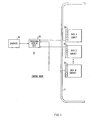
- the processor/display unit 20 processes and displays data received from the data sources DS of the remote data locations herein illustrated as consisting of data cabinets, A, B, ...N, and provides the processed data for access by a central computer 40.
- the remote data locations as represented by data cabinets A, B, etc. can represent any of numerous sources of data information with the data sources DS being groups of control rods within the containment C of the nuclear power plant.
- the processor/display unit 20 functions as a data correlator and local display of processed data. Parallel multiplexing is used to obtain data from the data cabinets A, B, etc.
- the processing section of the unit 20 generates a sequence of addresses corresponding to the data sources DS and sequentially processes the data for display purposes. Raw data from the data cabinets is also fed to a random access memory in a display unit-to-computer interface 32 ( Figure 2) for storage.
- the central computer 40 accesses the random access memory on a non-synchronous or random basis, i.e., the computer requests data corresponding to a computer address which is independent of the display address generated by the processor/display unit 20 to access the data cabinets.
- the processor/display unit 20 responds to the address reqest from the central computer 40 and initiates a data search in its memory within a specifically allocated time period.
- the invention resides in a digital display exerciser for a data acquisition and storage system wherein data from at least one data source is not only processed for display but also is stored for computer address access of the data in response to periodically generated display addresses
- said data acquisition and storage system including a data processor means having an input and an output, and including means for generating display addresses for addressing said at least one data source and causing data from said data source to be supplied to the input of said data processor means, a display means operatively coupled to the output of said data processor means to provide a visual display of the data processed by said data processor means, a storage means for retaining in storage locations corresponding to the display addresses of said at least one data source the data from said data source, and means responsive to a computer address data request for accessing and reading out the data stored in said storage means at an address location corresponding to the computer address, said display exerciser being connected between the output of said storage means and the input of said data processor means, characterized in that said display exerciser includes data recirculating means for recirculating data from said storage means to the input
- a display exerciser which is connected in parallel with the display/processor means to recirculate the data stored in a RAM on the computer input/output interface card.
- This display exerciser also has the capability of permitting the operator to introduce simulated data input for the purpose of determining the operational integrity of the system as well as providing training opportunities for control room operators.
- data source of a remote data location is identified by an address, and the multiplexed data from each data source during a data scan of the remote data locations is processed for display purposes by the processor/display means during the first 3/4 of each address period.
- the multiplexed data is also stored in memory and is accessible for external interrogation by a central computer during the last 1/4 of the address.
- the display exerciser is synchronized to the addresses of the processor/display unit and increments the address by one, i.e., A+1. This action accomplishes the external interrogation of the memory of the interface means by selecting the next address during the first 1/4 of each address period and recirculating the data retrieved from that next address to the input of the display/processor unit. A delay in displaying the new data via the display exerciser will produce a result that is equal to one full data scan.
- the display exerciser not only provides the test capability but permits an operator to introduce new data for system evaluation or simulation purposes.
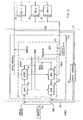
- the processor/display unit 20 is illustrated as consisting of processor 22, display means 24 and a computer input/output interface (or display unit-to-computer interface) circuit 30 which effectively acts as an extension of the computer 40 and operatively couples the processor circuit 22 to the computer 40.
- Each display address S generated by the processor circuit 22 is subdivided into four segments or sections S1, S2, S3 and S4 as illustrated in Figure 4.
- the address S functions to select the appropriate data source DS as well as initiate selection of the appropriate memory location in the random access memory 32 of the computer input/output interface 30 via a select circuit 34 which may be implemented as an OR gate.
- the S1 period allows for data delay and settling.
- the data from the appropriately addressed data cabinet is transmitted as data input to the processor circuit 22 for processing and display on the display means 24 as well as to the random access memory 32.
- the S3 period of the display address information displayed on display means 24 is refreshed and the presence of a computer address from the computer 40 is latched in latch oircuit 36 of the computer input/output circuit 30.
- the computer address is random and is not synchronized with the display address and thus need not correspond to the data information being addressed by the display address S of the processor circuit 22.
- the select circuit 34 gates the computer address from the latch circuit 36 to the random access memory 32.
- the display operation has been completed and the computer input/output circuit 30 completes a data search corresponding to the computer address which has latched in latch circuit 36 during the S3 period of the display address.
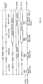
- FIG 4 The correlation of the display address format S with the computer address in the computer input/output circuit 30 is illustrated in Figure 4.
- the existing old data corresponding to the display address is latched during the S3 period and new data is written into the random access memory 32.
- the random access memory 32 responds to the computer address in latch circuit 36 and the computer requested data is retained in circuit 38 as data input of the computer 40.
- the processor/display unit 20 is disconnected from the data cabinets DS and the computer 40 and the display exerciser 50 of Figure 2 is operatively connected between data output of latch 38 and the inputs to the processor circuit 22 to permit recirculation of stored data and or the introduction of new data as determined by an operator.
- a reordering of the computer address is accomplished in the display exerciser 50 by incrementing the display address A by '' 1' ' .
- the display exerciser 50 is connected to the display address output of the processor unit 22 via a line 33 to receive the display address "A".
- the display exerciser is also connected to the computer address input of the computer input/output interface 30 through a line 35 to apply the incremented display address ("A+1") to the RAM 32 via the latch circuit 36 and the select circuit 34.
- A+1 incremented display address
- the computer address will retrieve the "old" data from the next address of the random access memory 32 and the data will be recirculated as "new" data via the processor circuit 22 during the next display address.
- This recirculated "new" data which is actually the "old” data in the random access memory 32 is then processed by the processing unit 22 and displayed by the display means 24.
- the capability of displaying the contents of the random access memory permits checking the operational integrity of the computer input/output interface 30.
- FIG. 3 there is schematically illustrated an implementation of the display exerciser 50.
- the data cabinets A and B of Figures 1 and 2 correspond to two groups X and Y of control rods wherein the control rods of group X are identified with addresses 1 through 10, and the control rods of group Y are identified with addresses 22 to 26.
- the thumbwheel switches 52 and 54 provide an operator with the capability of selecting a particular control rod of group X or group Y for introducing operating conditions corresponding to the selected data input via data input switches 72 and 74 -which are operatively associated with the control rod addresses of group X and group Y respectively.
- a display address A from the processor 22 is supplied to comparators 56 and 58 wherein it is compared to the preset address locations of thumbwheel switches 52 and 54.
- comparator 56 would generate a group X range enable signal which is gated through OR gate 60 to a one-shot multivibrator circuit 62.
- comparator circuit 58 will develop a group Y range enable output signal which is gated through OR gate 60 to the one-shot multivibrator circuit 62.
- the output of the one-shot multivibrator circuit 62 functions as a read/write strobe input to a random access memory 64.
- the group X range enable output of comparator circuit 56 and the group Y range enable output of the comparator circuit 58 serve as inputs to AND gates 80 and 82 respectively.
- the group X range enable signal supplied to AND gate 80 will gate the data developed by preset data input switches 72 and counter 76 through OR gate 84 as data input to the random access memory 64. This data is written into each location in the random access memory 64 corresponding to the display address A and is sequentially read out from the memory to be supplied to the processor 22 via switch 90.
- the group Y range enable output of the comparator circuit 58 will gate data from data input switches 74 and counter 78 through OR gate 84 as data input to the random access memory 64 to be written at the address location corresponding to display address A.
- the counters 76 and 78 are illustrated as up/down counters which are clocked at a predetermined clock rate signal.
- the data input to the random access memory 64 may be clocked in either an increasing or decreasing count mode from the preset level set in switches 72 and 74 as determined by the up or down count mode of the counters 76 and 78 respectively.
- the positioning of the operator control switch 90 in position P 1 provides for recirculation of stored data from the random access memory 32 of the interface circuit 30 as input data to the processor 22. Whenever "simulated" data stored in the random access memory 64 is to be fed to the processor 22, the switch 90 is automatically moved to the position P2 where the recirculated data is blocked from reaching the input of the processor 22.
- the computer address for the processor/display circuit corresponds to the display address A incremented by 1, i.e., A+ 1, and is supplied to the select circuit 34 of the processor/display circuitry 20.
- the display exerciser in the operation of the display exerciser as described above the data cabinets DS and the computer 4D remain disconnected from the processor/display unit 20.
- the display exerciser recirculates the data stored in the random access memory 32 back to the input of the processor/display unit 20 in synchronism with the display address to permit checking of the operational integrity of the computer input/output interface 30.
- the display exerciser 50 can be used to introduce new data to the processor/display unit with the computer 40 connected thereto for simulation purposes to aid in the training of control room operators. In this latter case, the switch 90 remains in the P2 position.
Description
- This invention relates to a digital display exerciser for increasing the test and maintenance capability of a display unit-to-computer interface wherein the data in a memory in the interface is recirculated as simulated data from the interface output to the input of the display unit for display to enable checking of the operational integrity of the interface.
- In complex and sophisticated data acquisition and control systems, such as that associated with a nuclear power plant, data from numerous discrete locations within a facility is typically multiplexed through a data interface and processing unit for ultimate access and storage by a central data processing and control initiating computer. The requirement for operator awareness of the status of operating conditions within the facility necessitates the inclusion of a control room installation whereby an operator can monitor the facility conditions represented by the data being transmitted from the remote facility locations to the central computer.
- In the conventional arrangement, as shown in Figure 1, the processor/
display unit 20 processes and displays data received from the data sources DS of the remote data locations herein illustrated as consisting of data cabinets, A, B, ...N, and provides the processed data for access by acentral computer 40. The remote data locations, as represented by data cabinets A, B, etc. can represent any of numerous sources of data information with the data sources DS being groups of control rods within the containment C of the nuclear power plant. The processor/display unit 20 functions as a data correlator and local display of processed data. Parallel multiplexing is used to obtain data from the data cabinets A, B, etc. The processing section of theunit 20 generates a sequence of addresses corresponding to the data sources DS and sequentially processes the data for display purposes. Raw data from the data cabinets is also fed to a random access memory in a display unit-to-computer interface 32 (Figure 2) for storage. - The
central computer 40 accesses the random access memory on a non-synchronous or random basis, i.e., the computer requests data corresponding to a computer address which is independent of the display address generated by the processor/display unit 20 to access the data cabinets. The processor/display unit 20 responds to the address reqest from thecentral computer 40 and initiates a data search in its memory within a specifically allocated time period. - In the event that the processor/
display unit 20 is not operating properly, there will be a certain manifestation of a malfunction of the unit on the display screen. However, a problem arises where the display unit-to-computer interface 30 fails. There is no way of knowing the operational behavior of the interface except for the computer. It is desired to provide the test capability of the display unit-to-computer interface. - It is, therefore, an object of this invention to provide a novel digital display exerciser for a data acquisition and display system with a view to overcoming the deficiencies of the prior art.
- The invention resides in a digital display exerciser for a data acquisition and storage system wherein data from at least one data source is not only processed for display but also is stored for computer address access of the data in response to periodically generated display addresses, said data acquisition and storage system including a data processor means having an input and an output, and including means for generating display addresses for addressing said at least one data source and causing data from said data source to be supplied to the input of said data processor means, a display means operatively coupled to the output of said data processor means to provide a visual display of the data processed by said data processor means, a storage means for retaining in storage locations corresponding to the display addresses of said at least one data source the data from said data source, and means responsive to a computer address data request for accessing and reading out the data stored in said storage means at an address location corresponding to the computer address, said display exerciser being connected between the output of said storage means and the input of said data processor means, characterized in that said display exerciser includes data recirculating means for recirculating data from said storage means to the input of said data processor means in accordance with the display addresses generated by said data processor means, whereby the recirculated data is displayed by said display means thus permitting checking of the operational integrity of said storage means as well as said stored data access means.
- In accordance with a preferred embodiment of the present invention, there is provided a display exerciser which is connected in parallel with the display/processor means to recirculate the data stored in a RAM on the computer input/output interface card. This display exerciser also has the capability of permitting the operator to introduce simulated data input for the purpose of determining the operational integrity of the system as well as providing training opportunities for control room operators.
- In the normal operation of the data acquisition and display system, data source of a remote data location is identified by an address, and the multiplexed data from each data source during a data scan of the remote data locations is processed for display purposes by the processor/display means during the first 3/4 of each address period. The multiplexed data is also stored in memory and is accessible for external interrogation by a central computer during the last 1/4 of the address. When there is any maintenance or testing operation to be desired or any time the plant is down not using the computer, the display exerciser is connected in parallel with the display/processor unit while the data source of the remote data location as well as the computer is disconnected from the display/processor unit. The display exerciser is synchronized to the addresses of the processor/display unit and increments the address by one, i.e., A+1. This action accomplishes the external interrogation of the memory of the interface means by selecting the next address during the first 1/4 of each address period and recirculating the data retrieved from that next address to the input of the display/processor unit. A delay in displaying the new data via the display exerciser will produce a result that is equal to one full data scan.
- The display exerciser not only provides the test capability but permits an operator to introduce new data for system evaluation or simulation purposes.
- The invention will become more readily apparent from the following exemplary description in connection with the accompanying drawings:
- Figure 1 is a block diagram schematic illustration of a data acquisition system;
- Figure 2 is a schematic illustration of the processor/display circuitry of the system of Figure 1 showing how the display exerciser according to this invention is connected;
- Figure 3 is a schematic illustration of the combination of the display exerciser and processor/display circuitry of Figure 1;
- Figure 4 is an illustration of an address period of the system of Figure 1; and
- Figure 5 is an illustration of the reordering of the computer address accomplished by incrementing the address by "+1" as accomplished by the display exerciser of Figure 3.
- Referring to Figure 2, the processor/
display unit 20 is illustrated as consisting ofprocessor 22, display means 24 and a computer input/output interface (or display unit-to-computer interface)circuit 30 which effectively acts as an extension of thecomputer 40 and operatively couples theprocessor circuit 22 to thecomputer 40. Each display address S generated by theprocessor circuit 22 is subdivided into four segments or sections S1, S2, S3 and S4 as illustrated in Figure 4. The address S functions to select the appropriate data source DS as well as initiate selection of the appropriate memory location in therandom access memory 32 of the computer input/output interface 30 via aselect circuit 34 which may be implemented as an OR gate. - The S1 period allows for data delay and settling. During the S2 period, the data from the appropriately addressed data cabinet is transmitted as data input to the
processor circuit 22 for processing and display on the display means 24 as well as to therandom access memory 32. During the S3 period of the display address, information displayed on display means 24 is refreshed and the presence of a computer address from thecomputer 40 is latched inlatch oircuit 36 of the computer input/output circuit 30. As described above, the computer address is random and is not synchronized with the display address and thus need not correspond to the data information being addressed by the display address S of theprocessor circuit 22. Theselect circuit 34 gates the computer address from thelatch circuit 36 to therandom access memory 32. During the S4 period of the display address S, the display operation has been completed and the computer input/output circuit 30 completes a data search corresponding to the computer address which has latched inlatch circuit 36 during the S3 period of the display address. - The correlation of the display address format S with the computer address in the computer input/
output circuit 30 is illustrated in Figure 4. Referring to Figure 4, during the S2 period of the display address, the existing old data corresponding to the display address is latched during the S3 period and new data is written into therandom access memory 32. During the S4 period, therandom access memory 32 responds to the computer address inlatch circuit 36 and the computer requested data is retained incircuit 38 as data input of thecomputer 40. - Where there is any maintenance or testing operation to be desired or any time the plant is down not using the
computer 40, the processor/display unit 20 is disconnected from the data cabinets DS and thecomputer 40 and thedisplay exerciser 50 of Figure 2 is operatively connected between data output oflatch 38 and the inputs to theprocessor circuit 22 to permit recirculation of stored data and or the introduction of new data as determined by an operator. In order to allow for synchronization of the computer input/output circuit 30 with theprocessing section 22 of theunit 20, a reordering of the computer address is accomplished in thedisplay exerciser 50 by incrementing the display address A by '' 1' ' . Thedisplay exerciser 50 is connected to the display address output of theprocessor unit 22 via aline 33 to receive the display address "A". The display exerciser is also connected to the computer address input of the computer input/output interface 30 through aline 35 to apply the incremented display address ("A+1") to theRAM 32 via thelatch circuit 36 and theselect circuit 34. With this reordering of computer address, the computer address will retrieve the "old" data from the next address of therandom access memory 32 and the data will be recirculated as "new" data via theprocessor circuit 22 during the next display address. This recirculated "new" data which is actually the "old" data in therandom access memory 32 is then processed by theprocessing unit 22 and displayed by the display means 24. The capability of displaying the contents of the random access memory permits checking the operational integrity of the computer input/output interface 30. - Referring to Figure 3 there is schematically illustrated an implementation of the
display exerciser 50. For the purposes of discussion it will be assumed that the data cabinets A and B of Figures 1 and 2 correspond to two groups X and Y of control rods wherein the control rods of group X are identified withaddresses 1 through 10, and the control rods of group Y are identified withaddresses 22 to 26. Thus, thethumbwheel switches 52 and 54 provide an operator with the capability of selecting a particular control rod of group X or group Y for introducing operating conditions corresponding to the selected data input viadata input switches 72 and 74 -which are operatively associated with the control rod addresses of group X and group Y respectively. A display address A from theprocessor 22 is supplied tocomparators thumbwheel switches 52 and 54. In the event the address A is within the group X address range of 1 to 10,comparator 56 would generate a group X range enable signal which is gated throughOR gate 60 to a one-shot multivibrator circuit 62. In the event that address A corresponds to an address location between 22 and 26,comparator circuit 58 will develop a group Y range enable output signal which is gated throughOR gate 60 to the one-shot multivibrator circuit 62. The output of the one-shot multivibrator circuit 62 functions as a read/write strobe input to arandom access memory 64. The group X range enable output ofcomparator circuit 56 and the group Y range enable output of thecomparator circuit 58 serve as inputs toAND gates gate 80 will gate the data developed by presetdata input switches 72 and counter 76 through ORgate 84 as data input to therandom access memory 64. This data is written into each location in therandom access memory 64 corresponding to the display address A and is sequentially read out from the memory to be supplied to theprocessor 22 viaswitch 90. - In the event address A corresponds to a group Y address, the group Y range enable output of the
comparator circuit 58 will gate data fromdata input switches 74 and counter 78 through ORgate 84 as data input to therandom access memory 64 to be written at the address location corresponding to display address A. Thecounters random access memory 64 may be clocked in either an increasing or decreasing count mode from the preset level set inswitches counters - The positioning of the
operator control switch 90 inposition P 1 provides for recirculation of stored data from therandom access memory 32 of theinterface circuit 30 as input data to theprocessor 22. Whenever "simulated" data stored in therandom access memory 64 is to be fed to theprocessor 22, theswitch 90 is automatically moved to the position P2 where the recirculated data is blocked from reaching the input of theprocessor 22. - The computer address for the processor/display circuit corresponds to the display address A incremented by 1, i.e.,
A+ 1, and is supplied to theselect circuit 34 of the processor/display circuitry 20. - It should be borne in mind that in the operation of the display exerciser as described above the data cabinets DS and the computer 4D remain disconnected from the processor/
display unit 20. The display exerciser recirculates the data stored in therandom access memory 32 back to the input of the processor/display unit 20 in synchronism with the display address to permit checking of the operational integrity of the computer input/output interface 30. However, it should be noted also that thedisplay exerciser 50 can be used to introduce new data to the processor/display unit with thecomputer 40 connected thereto for simulation purposes to aid in the training of control room operators. In this latter case, theswitch 90 remains in the P2 position. -


Claims (4)
Applications Claiming Priority (2)
| Application Number | Priority Date | Filing Date | Title |
|---|---|---|---|
| US95035878A | 1978-10-11 | 1978-10-11 | |
| US950358 | 1978-10-11 |
Publications (3)
| Publication Number | Publication Date |
|---|---|
| EP0009828A2 EP0009828A2 (en) | 1980-04-16 |
| EP0009828A3 EP0009828A3 (en) | 1980-04-30 |
| EP0009828B1 true EP0009828B1 (en) | 1982-09-15 |
Family
ID=25490337
Family Applications (1)
| Application Number | Title | Priority Date | Filing Date |
|---|---|---|---|
| EP79103894A Expired EP0009828B1 (en) | 1978-10-11 | 1979-10-10 | Digital display exerciser |
Country Status (6)
| Country | Link |
|---|---|
| US (1) | US4330843A (en) |
| EP (1) | EP0009828B1 (en) |
| JP (1) | JPS5553733A (en) |
| CA (1) | CA1134050A (en) |
| DE (1) | DE2963685D1 (en) |
| ES (1) | ES8105493A1 (en) |
Families Citing this family (6)
| Publication number | Priority date | Publication date | Assignee | Title |
|---|---|---|---|---|
| DE3071062D1 (en) * | 1980-11-26 | 1985-10-10 | Ibm | A method of testing a display apparatus |
| JPS592086A (en) * | 1982-06-28 | 1984-01-07 | 株式会社日立製作所 | Matrix display driving circuit |
| CA1254683A (en) * | 1985-05-17 | 1989-05-23 | Kevin P. Staggs | On-line verification of video display generator |
| JPH0285927A (en) * | 1988-09-22 | 1990-03-27 | Hitachi Vlsi Eng Corp | Memory device |
| KR100191566B1 (en) * | 1989-11-02 | 1999-06-15 | 뮬홀란드 죤 에이취 | Indicator validation method in control complex of nuclear power plant |
| US5267277A (en) * | 1989-11-02 | 1993-11-30 | Combustion Engineering, Inc. | Indicator system for advanced nuclear plant control complex |
Family Cites Families (12)
| Publication number | Priority date | Publication date | Assignee | Title |
|---|---|---|---|---|
| US3623005A (en) * | 1967-08-01 | 1971-11-23 | Ultronic Systems Corp | Video display apparatus employing a combination of recirculating buffers |
| DE1952175C3 (en) * | 1968-10-23 | 1978-06-15 | Ing. C. Olivetti & C., S.P.A., Ivrea, Turin (Italien) | Control arrangement for the display of data characters in tabular form |
| US3579196A (en) * | 1969-02-14 | 1971-05-18 | Bunker Ramo | Data storage and display system |
| US3936885A (en) * | 1973-02-23 | 1976-02-03 | Westinghouse Electric Corporation | Training simulator and method for nuclear power plant heater and non-linear modeling |
| US3895357A (en) * | 1973-02-23 | 1975-07-15 | Ibm | Buffer memory arrangement for a digital television display system |
| US4053951A (en) * | 1973-08-06 | 1977-10-11 | Amsco/Medical Electronics, Inc. | Data acquisition, storage and display system |
| US3942157A (en) * | 1974-01-22 | 1976-03-02 | Azurdata Inc. | Data gathering formatting and transmitting system having portable data collecting device |
| JPS5830587B2 (en) * | 1974-09-25 | 1983-06-30 | 富士通株式会社 | Online Hiyouji Seigyo System |
| US4090247A (en) * | 1975-08-11 | 1978-05-16 | Arthur D. Little, Inc. | Portable data entry device |
| DE2551981C3 (en) * | 1975-11-19 | 1978-07-27 | Siemens Ag, 1000 Berlin Und 8000 Muenchen | Test arrangement for a data output device |
| JPS52130210A (en) * | 1976-04-24 | 1977-11-01 | Fujitsu Ltd | Subscriber condition display control system |
| DE2638349C2 (en) * | 1976-08-26 | 1984-01-12 | Leuze Electronic Kg, 7311 Owen | Arrangement for the computer-compatible acquisition, storage and evaluation of production data |
-
1979
- 1979-10-10 EP EP79103894A patent/EP0009828B1/en not_active Expired
- 1979-10-10 CA CA337,260A patent/CA1134050A/en not_active Expired
- 1979-10-10 DE DE7979103894T patent/DE2963685D1/en not_active Expired
- 1979-10-10 ES ES484921A patent/ES8105493A1/en not_active Expired
- 1979-10-11 JP JP13007979A patent/JPS5553733A/en active Granted
- 1979-12-04 US US06/100,171 patent/US4330843A/en not_active Expired - Lifetime
Also Published As
| Publication number | Publication date |
|---|---|
| US4330843A (en) | 1982-05-18 |
| JPS6346432B2 (en) | 1988-09-14 |
| EP0009828A3 (en) | 1980-04-30 |
| ES484921A0 (en) | 1981-05-16 |
| ES8105493A1 (en) | 1981-05-16 |
| CA1134050A (en) | 1982-10-19 |
| DE2963685D1 (en) | 1982-11-04 |
| JPS5553733A (en) | 1980-04-19 |
| EP0009828A2 (en) | 1980-04-16 |
Similar Documents
| Publication | Publication Date | Title |
|---|---|---|
| US4094000A (en) | Graphics display unit | |
| US4626837A (en) | Display interface apparatus | |
| US5361346A (en) | Portable tester (qualifier) for evaluating and testing SCSI interface magnetic disc drives in accordance with ANSI SCSI-A and SCSI-2 definitions | |
| US3831149A (en) | Data monitoring apparatus including a plurality of presettable control elements for monitoring preselected signal combinations and other conditions | |
| EP0009828B1 (en) | Digital display exerciser | |
| US4070705A (en) | Simulation apparatus | |
| DE3520649A1 (en) | NUCLEAR SYSTEM TEST SIMULATOR | |
| CN101727373A (en) | Display card testing device and method | |
| EP0202865B1 (en) | Testable video display generator | |
| US5235530A (en) | Active cartridge display for hardware modeler | |
| CN102402482A (en) | Test system and method | |
| Busse et al. | Concept and Status of the Control System for the VICKSI Accelerators at HMI-Berlin | |
| EP0470768B1 (en) | Scheduling drawing operations of moving images | |
| JP3035957B2 (en) | Diagnosis method of display data | |
| McCracken et al. | An economical tonal display for interactive graphics and image analysis data | |
| RU77707U1 (en) | AUTOMATED SYSTEM OF THE JUDICIAL DECISION BANK (JUDICIAL PRACTICE) OF THE FEDERAL COURTS OF GENERAL JURISDICTION | |
| JPH0443594B2 (en) | ||
| Heinze | The PS Interface for the Transfer Line SD26 | |
| DE2850606A1 (en) | ARRANGEMENT FOR COMPUTER CONTROLLED EXECUTION OF A SEQUENCE OF ELECTRICAL TESTS ON A SYSTEM TO BE CHECKED | |
| JP3035958B2 (en) | Diagnosis method of display data | |
| JPS62280667A (en) | Fault diagnosing device | |
| SU1583967A1 (en) | Device for presentation of information on screen of television receiver | |
| JPS63249885A (en) | Data display for evaluation | |
| KR940001833B1 (en) | Digital video apparatus | |
| RU122504U1 (en) | AUTOMATED WORK PLACE OF THE PARTICIPANT OF THE LEGISLATIVE ACTIVITY OF THE STATE AUTOMATED SYSTEM "LEGISLATION" |
Legal Events
| Date | Code | Title | Description |
|---|---|---|---|
| PUAI | Public reference made under article 153(3) epc to a published international application that has entered the european phase |
Free format text: ORIGINAL CODE: 0009012 |
|
| PUAL | Search report despatched |
Free format text: ORIGINAL CODE: 0009013 |
|
| AK | Designated contracting states |
Designated state(s): BE DE FR GB IT |
|
| AK | Designated contracting states |
Designated state(s): BE DE FR GB IT |
|
| 17P | Request for examination filed |
Effective date: 19801006 |
|
| ITF | It: translation for a ep patent filed |
Owner name: ING. ZINI MARANESI & C. S.R.L. |
|
| GRAA | (expected) grant |
Free format text: ORIGINAL CODE: 0009210 |
|
| AK | Designated contracting states |
Designated state(s): BE DE FR GB IT |
|
| REF | Corresponds to: |
Ref document number: 2963685 Country of ref document: DE Date of ref document: 19821104 |
|
| PGFP | Annual fee paid to national office [announced via postgrant information from national office to epo] |
Ref country code: DE Payment date: 19830725 Year of fee payment: 5 |
|
| PGFP | Annual fee paid to national office [announced via postgrant information from national office to epo] |
Ref country code: FR Payment date: 19830726 Year of fee payment: 5 |
|
| PGFP | Annual fee paid to national office [announced via postgrant information from national office to epo] |
Ref country code: BE Payment date: 19830831 Year of fee payment: 5 |
|
| PG25 | Lapsed in a contracting state [announced via postgrant information from national office to epo] |
Ref country code: BE Effective date: 19841031 |
|
| BERE | Be: lapsed |
Owner name: WESTINGHOUSE ELECTRIC CORP. Effective date: 19841010 |
|
| GBPC | Gb: european patent ceased through non-payment of renewal fee | ||
| PG25 | Lapsed in a contracting state [announced via postgrant information from national office to epo] |
Ref country code: FR Free format text: LAPSE BECAUSE OF NON-PAYMENT OF DUE FEES Effective date: 19850628 |
|
| PG25 | Lapsed in a contracting state [announced via postgrant information from national office to epo] |
Ref country code: DE Effective date: 19850702 |
|
| REG | Reference to a national code |
Ref country code: FR Ref legal event code: ST |
|
| PG25 | Lapsed in a contracting state [announced via postgrant information from national office to epo] |
Ref country code: GB Effective date: 19881118 |
|
| ITTA | It: last paid annual fee | ||
| PLBE | No opposition filed within time limit |
Free format text: ORIGINAL CODE: 0009261 |
|
| STAA | Information on the status of an ep patent application or granted ep patent |
Free format text: STATUS: NO OPPOSITION FILED WITHIN TIME LIMIT |