EP0004457A2 - Processing method and circuit for PAL colour television signals - Google Patents
Processing method and circuit for PAL colour television signals Download PDFInfo
- Publication number
- EP0004457A2 EP0004457A2 EP79300449A EP79300449A EP0004457A2 EP 0004457 A2 EP0004457 A2 EP 0004457A2 EP 79300449 A EP79300449 A EP 79300449A EP 79300449 A EP79300449 A EP 79300449A EP 0004457 A2 EP0004457 A2 EP 0004457A2
- Authority
- EP
- European Patent Office
- Prior art keywords
- signal
- output
- band
- circuit
- chrominance
- Prior art date
- Legal status (The legal status is an assumption and is not a legal conclusion. Google has not performed a legal analysis and makes no representation as to the accuracy of the status listed.)
- Granted
Links
Images


Classifications
-
- H—ELECTRICITY
- H04—ELECTRIC COMMUNICATION TECHNIQUE
- H04N—PICTORIAL COMMUNICATION, e.g. TELEVISION
- H04N9/00—Details of colour television systems
- H04N9/77—Circuits for processing the brightness signal and the chrominance signal relative to each other, e.g. adjusting the phase of the brightness signal relative to the colour signal, correcting differential gain or differential phase
- H04N9/78—Circuits for processing the brightness signal and the chrominance signal relative to each other, e.g. adjusting the phase of the brightness signal relative to the colour signal, correcting differential gain or differential phase for separating the brightness signal or the chrominance signal from the colour television signal, e.g. using comb filter
Definitions
- This invention relates to circuits for processing colour television signals in the PAL or N.T.S.C. system.
- This invention enables the provision of a processing system in which line-locked sampling can be used, and which is of relatively uncomplicated construction. At the least, the invention provides a useful alternative to the previously known systems. Apart from separating a composite PAL signal into its luminance and chrominance components, the system may also be useful in filtering the luminance component of a PAL signal to remove components likely to cause cross-colour, or in filtering a combination of the luminance and chrominance components in a PAL coder.
- a signal processing circuit for processing colour television signals in the PAL or N.T.S.C. system, comprising an input terminal, means connected to the input signal for providing (i) a first signal being the input signal delayed by one line period and (ii) a second signal being the resultant of the average of the undelayed input signal and the input signal delayed by two line periods subtracted from the first signal, and means for band-pass filtering the second signal to provide a filtered signal, the filter pass-band comprising essentially the chrominance frequency band of the system.
- Preferably means are provided for combining the first signal and the filtered signal such as to subtract chrominance components or components resembling them in the filtered signal from the said first signal, and a main output terminal is connected to the output of the combining means.
- a second output terminal may then be connected to the output of the filtering means.
- a composite PAL or N.T.S.C. signal is applied to the input terminal, the luminance component will appear at the main output terminal and the chrominance component will appear at the second output terminal. In any given instance, only one of the outputs may be used.
- the processing circuit 10 of Fig. 1 has an input terminal 12 to which are connected two one-line delays 14 and 16 in series.
- An averaging circuit 18 conveniently formed of an adder and a divide-by-two circuit is connected both to the input terminal 12 and to the output of delay 16 to provide a signal representing the average of the undelayed input signal and the input signal delayed by two line periods.
- At the output of delay 14 is provided the input signal delayed by one line period.
- a subtractor 20 has its inverting input connected to the output of the averaging circuit 18, and its non-inverting input connected to the output of the delay 14. It will be appreciated that the averaging circuit 18 and subtractor 20 can if desired be combined into a single three-input weighted adder, the weights being -2, +1, -i.
- a band-pass filter 22 having a pass-band covering the chrominance frequency band. In the PAL system in use in the United Kingdom this extends from about 3.3 MHz to about 5.5 MHz.
- the output of the filter 22 is applied to the inverting input of a subtractor 24, the non-inverting input of which is connected to the output of the delay 14.
- the output 26 of the subtractor 24 constitutes the main output of the circuit, and the output 28 of the filter 22 will also frequently be used as a subsidiary output, as will be described.
- circuit with a composite PAL signal applied to the input terminal will be described by considering separately the processing of chrominance components, of purely horizontal luminance components (such as formed by vertical bars), and of purely vertical luminance components (such as formed by horizontal bars). Reference will be made to the circuit junctions A, B, C, D and E shown on Fig. 1.
- the phase of the U and V subcarrier is reversed across the two delay lines, as between points A and C, by virtue of the properties of the PAL system, since in the PAL system the colour subcarrier frequency is approximately an odd integral multiple of one quarter of the line frequency.
- the averagerl8 produces zero output at point D, and the chrominance component from point B at the output of delay 14 passes through the subtractor 20 unaltered and after filtering in filter 22 is subtracted in subtractor 24 to leave no nett chrominance component in the luminance output at terminal 26.
- the chrominance component itself is available at terminal 28.
- the signals at A, B, C and D are all equal, there being no difference between adjacent lines. Therefore the signals at points D and B cancel out in the subtractor 20. Thus no luminance component reaches the band-pass filter 22. Since there is no signal at point E, the luminance component from point B is passed directly to the luminance output 26.
- Luminance components containing purely vertical frequencies are unable to pass the band-pass filter 22, and likewise do not appear at point E.
- the input signal is separated into a luminance component appearing at the output 26 and a chrominance component appearing at the output 28. It is impossible to separate the luminance and chrominance completely because the two spectra overlap. However, we have found that with the circuit described subjectively good separation is obtained.
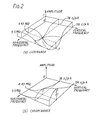
- the frequency responses of the circuit of Fig. 1 to the luminance and chrominance components are shown respectively at (a) and (b) in Fig. 2.
- the diagrams show 3-dimensional plots of transmitted amplitude as against both horizontal frequency (in MHz) and vertical frequency (in cycles per picture height; c/p.h.).
- the response falls to zero at the chrominance subcarrier frequency of 4.43 MHz and at 78 c/p.h. It is seen that some of the high frequency diagonal luminance is inverted.
- the response is unity at 4.43 MHz and 78 c/p.h.
- the vertical frequency response at the horizontal subcarrier frequency is anti-symmetrical about the vertical subcarrier frequency. Because of this, there will be no loss of vertical resolution in the demodulated U and V signals since any loss in the lower sideband is countered by a gain in the upper sideband. However, the anti-symmetric response will cause cross-talk between U and V on vertical colour changes. Because the cross-talk components will be modulated by the PAL switch, their effects can be reduced by vertical low-pass filtering of the demodulated U and V signals, although this will cause some loss of vertical resolution.
- the chrominance and luminance separation filter 10 illustrated in Fig. 1 shows good separation of chrominance and luminance whilst maintaining the vertical chrominance resolution.
- the filter could be implemented as either an analogue circuit or digitally, using line-locked sampling.
- the digital implementation can be straightforward, since, apart from the horizontal chrominance filter, only simple arithmetic operations are involved.
- the circuit of Fig. 1 can be used to "clean-up" a luminance signal alone before processing in situations where cross-talk is likely to arise.
- output 28 is not used.
- Fig. 3 shows the use of the circuit of Fig. 1 in a PAL coder.
- the coder 30 of Fig. 3 has an input 32 for receiving a luminance signal and an input 34 for receiving a chrominance signal.
- the luminance signal is subtracted from the chrominance signal in a subtractor 36 and the resultant applied to the input 12 of the circuit 10 of Fig. 1.
- An adder 38 receives the output 28 from the circuit 10 and also the luminance signal from input 32 after passage through a compensating delay 40, and provides an encoded PAL signal at an output 42.
- the subtractor 24 can be omitted from the circuit 10 of Fig. 1.
- the operation of the circuit of Fig. 3 is as follows.
- the modulated U and V subcarrier signals pass through the subtractor 36 to input 12 of Fig. 1, the circuit of which operates as a two- dimensional chrominance band-pass filter.
- the chrominance signal corresponding to an area of constant colour is unattenuated, but chrominance sidebands are shaped by the characteristic of Fig. 2(b). This tends to exclude chrominance that would be interpreted as 1 finance at the decoder.
- the remaining chrominance is added to the luminance signal Y in adder 38 to form the composite PAL signal.
- the circuit 10 also affects the Y signal applied at input 32.
- the effect of the subtractor 36 is to invert the Y signal which then passes to the chrominance band-pass filter of Fig. 1. Any luminance signals that appear at output 28 are those which would be interpreted incorrectly as chrominance at the decoder. Since these signals have been inverted, they cancel the unwanted components when combined by adder 38 with the direct luminance signal passing through the compensating delay 40.
- Fig. 3 the effect of Fig. 3 is to remove at the coder many of the components that would cause cross-colour and cross luminance in the decoded signals.
- the apparatus is particularly suited for use with PAL signals, although it can be adapted for use with N.T.S.C. signals.
- the circuit of Fig. 1 is modified to give the processing circuit 50 shown in Fig. 4, by the addition of a divide-by-two circuit 52 between the subtractor 20 and the junction E, either before or after the band-pass filter 22, and alteration of the band-pass filter to be centred on the correct colour subcarrier frequency, e.g. 3.58 MHz for a conventional 525/60 system.
- a digital sampler 54 which samples at a line-locked sample rate.
- the circuit is the same as Fig. 1.
Abstract
Description
- This invention relates to circuits for processing colour television signals in the PAL or N.T.S.C. system.
- It is frequently desired to separate a composite PAL colour television signal into its luminance and chrominance components. The simplest methods involve only band-pass filters, but these are crude, introduce considerable cross-colour, and largely negate many of the advantages of the PAL system. One improved method is described in our cognate British Patent Applications Nos. 22567/77 and 51668/77 (published as German Offenlegungsschrift 28 22 668), which uses delays of one line plus or minus a quarter cycle of subcarrier. Another improved method is described in our British Patent No. 1,511,230 and developed in our Patent No. 1,524,749 and Application No. 15811/77. However these improved methods are, at least in general, inapplicable to processing systems which use line-locked sampling and furthermore require relatively complicated circuitry.
- This invention enables the provision of a processing system in which line-locked sampling can be used, and which is of relatively uncomplicated construction. At the least, the invention provides a useful alternative to the previously known systems. Apart from separating a composite PAL signal into its luminance and chrominance components, the system may also be useful in filtering the luminance component of a PAL signal to remove components likely to cause cross-colour, or in filtering a combination of the luminance and chrominance components in a PAL coder.
- According to this invention there is provided a signal processing circuit for processing colour television signals in the PAL or N.T.S.C. system, comprising an input terminal, means connected to the input signal for providing (i) a first signal being the input signal delayed by one line period and (ii) a second signal being the resultant of the average of the undelayed input signal and the input signal delayed by two line periods subtracted from the first signal, and means for band-pass filtering the second signal to provide a filtered signal, the filter pass-band comprising essentially the chrominance frequency band of the system.
- Preferably means are provided for combining the first signal and the filtered signal such as to subtract chrominance components or components resembling them in the filtered signal from the said first signal, and a main output terminal is connected to the output of the combining means. A second output terminal may then be connected to the output of the filtering means. In this case, if a composite PAL or N.T.S.C. signal is applied to the input terminal, the luminance component will appear at the main output terminal and the chrominance component will appear at the second output terminal. In any given instance, only one of the outputs may be used.
- The invention will now be described in more detail, with reference to the accompanying drawings, in which
- Fig. 1 is a block circuit diagram of a processing circuit embodying the invention for use with PAL signals;
- Fig. 2 shows at (a) the luminance and at (b) the chrominance characteristics of a filter of the type shown in Fig. 1 when supplied with a composite PAL signal;
- Fig. 3 shows how the circuit of Fig. 1 can be incorporated into a PAL coder; and
- Fig. 4 is a block diagram of a circuit based on Fig. 1 for N.T.S.C. signals.
- The
processing circuit 10 of Fig. 1 has aninput terminal 12 to which are connected two one-line delays averaging circuit 18 conveniently formed of an adder and a divide-by-two circuit is connected both to theinput terminal 12 and to the output ofdelay 16 to provide a signal representing the average of the undelayed input signal and the input signal delayed by two line periods. At the output ofdelay 14 is provided the input signal delayed by one line period. - A
subtractor 20 has its inverting input connected to the output of theaveraging circuit 18, and its non-inverting input connected to the output of thedelay 14. It will be appreciated that theaveraging circuit 18 andsubtractor 20 can if desired be combined into a single three-input weighted adder, the weights being -2, +1, -i. - To the output of
subtractor 20 is connected a band-pass filter 22 having a pass-band covering the chrominance frequency band. In the PAL system in use in the United Kingdom this extends from about 3.3 MHz to about 5.5 MHz. The output of thefilter 22 is applied to the inverting input of asubtractor 24, the non-inverting input of which is connected to the output of thedelay 14. Theoutput 26 of thesubtractor 24 constitutes the main output of the circuit, and theoutput 28 of thefilter 22 will also frequently be used as a subsidiary output, as will be described. - The use of the circuit with a composite PAL signal applied to the input terminal will be described by considering separately the processing of chrominance components, of purely horizontal luminance components (such as formed by vertical bars), and of purely vertical luminance components (such as formed by horizontal bars). Reference will be made to the circuit junctions A, B, C, D and E shown on Fig. 1.
- For an area of constant colour, the phase of the U and V subcarrier is reversed across the two delay lines, as between points A and C, by virtue of the properties of the PAL system, since in the PAL system the colour subcarrier frequency is approximately an odd integral multiple of one quarter of the line frequency. Thus the averagerl8 produces zero output at point D, and the chrominance component from point B at the output of
delay 14 passes through thesubtractor 20 unaltered and after filtering infilter 22 is subtracted insubtractor 24 to leave no nett chrominance component in the luminance output atterminal 26. The chrominance component itself is available atterminal 28. - For luminance components containing horizontal frequencies, the signals at A, B, C and D are all equal, there being no difference between adjacent lines. Therefore the signals at points D and B cancel out in the
subtractor 20. Thus no luminance component reaches the band-pass filter 22. Since there is no signal at point E, the luminance component from point B is passed directly to theluminance output 26. - Luminance components containing purely vertical frequencies are unable to pass the band-
pass filter 22, and likewise do not appear at point E. - It is thus seen that the input signal is separated into a luminance component appearing at the
output 26 and a chrominance component appearing at theoutput 28. It is impossible to separate the luminance and chrominance completely because the two spectra overlap. However, we have found that with the circuit described subjectively good separation is obtained. - The frequency responses of the circuit of Fig. 1 to the luminance and chrominance components are shown respectively at (a) and (b) in Fig. 2. The diagrams show 3-dimensional plots of transmitted amplitude as against both horizontal frequency (in MHz) and vertical frequency (in cycles per picture height; c/p.h.).
- For the luminance output the response falls to zero at the chrominance subcarrier frequency of 4.43 MHz and at 78 c/p.h. It is seen that some of the high frequency diagonal luminance is inverted.
- For the chrominance output the response is unity at 4.43 MHz and 78 c/p.h. The vertical frequency response at the horizontal subcarrier frequency is anti-symmetrical about the vertical subcarrier frequency. Because of this, there will be no loss of vertical resolution in the demodulated U and V signals since any loss in the lower sideband is countered by a gain in the upper sideband. However, the anti-symmetric response will cause cross-talk between U and V on vertical colour changes. Because the cross-talk components will be modulated by the PAL switch, their effects can be reduced by vertical low-pass filtering of the demodulated U and V signals, although this will cause some loss of vertical resolution.
- The chrominance and
luminance separation filter 10 illustrated in Fig. 1 shows good separation of chrominance and luminance whilst maintaining the vertical chrominance resolution. The filter could be implemented as either an analogue circuit or digitally, using line-locked sampling. The digital implementation can be straightforward, since, apart from the horizontal chrominance filter, only simple arithmetic operations are involved. - The circuit of Fig. 1 can be used to "clean-up" a luminance signal alone before processing in situations where cross-talk is likely to arise. For this
purpose output 28 is not used. - Fig. 3 shows the use of the circuit of Fig. 1 in a PAL coder. The
coder 30 of Fig. 3 has aninput 32 for receiving a luminance signal and aninput 34 for receiving a chrominance signal. The luminance signal is subtracted from the chrominance signal in asubtractor 36 and the resultant applied to theinput 12 of thecircuit 10 of Fig. 1. Anadder 38 receives theoutput 28 from thecircuit 10 and also the luminance signal frominput 32 after passage through acompensating delay 40, and provides an encoded PAL signal at anoutput 42. As only theoutput 28 is used, thesubtractor 24 can be omitted from thecircuit 10 of Fig. 1. - The operation of the circuit of Fig. 3 is as follows. The modulated U and V subcarrier signals pass through the
subtractor 36 to input 12 of Fig. 1, the circuit of which operates as a two- dimensional chrominance band-pass filter. Atoutput 28, the chrominance signal corresponding to an area of constant colour is unattenuated, but chrominance sidebands are shaped by the characteristic of Fig. 2(b). This tends to exclude chrominance that would be interpreted as 1 finance at the decoder. The remaining chrominance is added to the luminance signal Y inadder 38 to form the composite PAL signal. - The
circuit 10 also affects the Y signal applied atinput 32. The effect of thesubtractor 36 is to invert the Y signal which then passes to the chrominance band-pass filter of Fig. 1. Any luminance signals that appear atoutput 28 are those which would be interpreted incorrectly as chrominance at the decoder. Since these signals have been inverted, they cancel the unwanted components when combined byadder 38 with the direct luminance signal passing through the compensatingdelay 40. - Therefore, the effect of Fig. 3 is to remove at the coder many of the components that would cause cross-colour and cross luminance in the decoded signals.
- The apparatus is particularly suited for use with PAL signals, although it can be adapted for use with N.T.S.C. signals. For use with N.T.S.C. signals, the circuit of Fig. 1 is modified to give the
processing circuit 50 shown in Fig. 4, by the addition of a divide-by-two circuit 52 between the subtractor 20 and the junction E, either before or after the band-pass filter 22, and alteration of the band-pass filter to be centred on the correct colour subcarrier frequency, e.g. 3.58 MHz for a conventional 525/60 system. It is assumed that digital signals are being processed as indicated by the inclusion of adigital sampler 54 which samples at a line-locked sample rate. In other respects the circuit is the same as Fig. 1.
Claims (5)
Applications Claiming Priority (2)
| Application Number | Priority Date | Filing Date | Title |
|---|---|---|---|
| GB1229478 | 1978-03-29 | ||
| GB1229478 | 1978-03-29 |
Publications (4)
| Publication Number | Publication Date |
|---|---|
| EP0004457A2 true EP0004457A2 (en) | 1979-10-03 |
| EP0004457A3 EP0004457A3 (en) | 1979-10-31 |
| EP0004457B1 EP0004457B1 (en) | 1983-09-07 |
| EP0004457B2 EP0004457B2 (en) | 1988-09-21 |
Family
ID=10001895
Family Applications (1)
| Application Number | Title | Priority Date | Filing Date |
|---|---|---|---|
| EP79300449A Expired EP0004457B2 (en) | 1978-03-29 | 1979-03-21 | Processing method and circuit for PAL colour television signals |
Country Status (4)
| Country | Link |
|---|---|
| US (1) | US4345268A (en) |
| EP (1) | EP0004457B2 (en) |
| JP (1) | JPS5946476B2 (en) |
| DE (1) | DE2966124D1 (en) |
Cited By (2)
| Publication number | Priority date | Publication date | Assignee | Title |
|---|---|---|---|---|
| EP0015134A1 (en) * | 1979-02-19 | 1980-09-03 | British Broadcasting Corporation | Method of and apparatus for coding and decoding PAL colour television signals |
| US5005074A (en) * | 1989-11-17 | 1991-04-02 | Rca Licensing Corporation | Adaptive multistandard video comb filter |
Families Citing this family (13)
| Publication number | Priority date | Publication date | Assignee | Title |
|---|---|---|---|---|
| JPS5799091A (en) * | 1980-12-11 | 1982-06-19 | Sony Corp | Separation circuit between luminance signal and carrier chrominance signal |
| NL8104101A (en) * | 1981-09-04 | 1983-04-05 | Philips Nv | PAL COMB FILTER. |
| US4456921A (en) * | 1981-12-02 | 1984-06-26 | Robert Bosch Gmbh | Comb filtering for NTSC television signals |
| DE3435264A1 (en) * | 1984-09-26 | 1986-04-03 | ANT Nachrichtentechnik GmbH, 7150 Backnang | METHOD FOR COMPATIBLE RESOLUTION ENHANCEMENT FOR COLOR TELEVISION TRANSMISSION SYSTEMS WITH REDUCTION OF CROSS-Crosstalk IN MOVEMENT-ADAPTIVE IMAGE PROCESSING |
| US4584599A (en) * | 1984-12-19 | 1986-04-22 | Scientific Atlanta, Inc. | Signal to noise ratio enhancement using baseband signals in an FM television system |
| US4893176A (en) * | 1985-10-09 | 1990-01-09 | Faroudja Y C | Adaptive comb filter for quadrature modulated color television systems |
| GB8622680D0 (en) * | 1986-09-19 | 1986-10-22 | Robinson R N | Decoder |
| US4731660A (en) * | 1987-02-20 | 1988-03-15 | Yves C. Faroudja | Processing methods using adaptive threshold for removal of chroma/luminance cross-talk in quadrature-modulated subcarrier color television systems |
| CA1303727C (en) * | 1987-08-28 | 1992-06-16 | Institut National De La Recherche Scientifique | Apparatus and method for encoding and decoding a ntsc color video signal |
| EP0313372B1 (en) * | 1987-10-21 | 1992-09-02 | Victor Company Of Japan, Limited | Yc separator for video signal processing circuit |
| CA2015587C (en) * | 1990-04-27 | 1996-12-03 | Chon Tam Le Dinh | Separable diamond shaped multidimensional filters for composite video endocing/decoding applications |
| US5103296A (en) * | 1990-04-30 | 1992-04-07 | U.S. Philips Corporation | Color television system having adaptive filters in the transmitter encoder and in the receiver decoder |
| JP3006850B2 (en) * | 1990-05-29 | 2000-02-07 | 松下電器産業株式会社 | Comb filter |
Citations (1)
| Publication number | Priority date | Publication date | Assignee | Title |
|---|---|---|---|---|
| US3858240A (en) * | 1971-01-11 | 1974-12-31 | Communications Satellite Corp | Reduced rate sampling process in pulse code modulation of analog signals |
Family Cites Families (10)
| Publication number | Priority date | Publication date | Assignee | Title |
|---|---|---|---|---|
| DE1941848C3 (en) * | 1969-08-16 | 1973-10-04 | Robert Bosch Fernsehanlagen Gmbh, 6100 Darmstadt | Method for separating the luminance and chrominance components in a PAL color television signal |
| US4056516A (en) * | 1971-12-28 | 1977-11-01 | Hoechst Aktiengesellschaft | Modacryl filaments and fibers and process for their manufacture |
| GB1431378A (en) * | 1972-04-19 | 1976-04-07 | Rca Corp | Colour information translating systems |
| GB1333887A (en) * | 1972-09-04 | 1973-10-17 | Pye Ltd | Separation of television signals |
| GB1582984A (en) * | 1976-08-09 | 1981-01-21 | Rca Corp | Video signal recording systems |
| US4143396A (en) * | 1977-01-26 | 1979-03-06 | Ampex Corporation | Digital chrominance separating and processing system and method |
| GB2003695B (en) * | 1977-09-01 | 1982-03-03 | British Broadcasting Corp | Method and apparatus for processing pal colour television signals in digital form |
| US4178609A (en) * | 1977-10-25 | 1979-12-11 | The Magnavox Company | Comb filter having improved luminance response |
| NL7803910A (en) * | 1978-04-13 | 1979-10-16 | Philips Nv | COMB FILTER CIRCUIT. |
| US4219842A (en) * | 1978-08-24 | 1980-08-26 | The Magnavox Company | Video signal combiner having a common phase response and independent amplitude response |
-
1979
- 1979-03-21 EP EP79300449A patent/EP0004457B2/en not_active Expired
- 1979-03-21 DE DE7979300449T patent/DE2966124D1/en not_active Expired
- 1979-03-27 JP JP54036187A patent/JPS5946476B2/en not_active Expired
-
1981
- 1981-01-26 US US06/228,547 patent/US4345268A/en not_active Expired - Lifetime
Patent Citations (1)
| Publication number | Priority date | Publication date | Assignee | Title |
|---|---|---|---|---|
| US3858240A (en) * | 1971-01-11 | 1974-12-31 | Communications Satellite Corp | Reduced rate sampling process in pulse code modulation of analog signals |
Non-Patent Citations (1)
| Title |
|---|
| IEEE TRANSACTIONS ON COMMUNICATION TECHNOLOGY, Vol. COM-19, Nr. 6, December 1971, New York, USA, GOLDING et al.: "Frequency interleaved sampling of a color television signal", pages 972-979 * |
Cited By (2)
| Publication number | Priority date | Publication date | Assignee | Title |
|---|---|---|---|---|
| EP0015134A1 (en) * | 1979-02-19 | 1980-09-03 | British Broadcasting Corporation | Method of and apparatus for coding and decoding PAL colour television signals |
| US5005074A (en) * | 1989-11-17 | 1991-04-02 | Rca Licensing Corporation | Adaptive multistandard video comb filter |
Also Published As
| Publication number | Publication date |
|---|---|
| US4345268A (en) | 1982-08-17 |
| EP0004457A3 (en) | 1979-10-31 |
| EP0004457B2 (en) | 1988-09-21 |
| JPS5946476B2 (en) | 1984-11-13 |
| EP0004457B1 (en) | 1983-09-07 |
| DE2966124D1 (en) | 1983-10-13 |
| JPS54133827A (en) | 1979-10-17 |
Similar Documents
| Publication | Publication Date | Title |
|---|---|---|
| US4072984A (en) | Chrominance-luminance separator | |
| US4345268A (en) | Processing circuit for color television signals | |
| GB1515551A (en) | Noise reduction in electrical signals | |
| JP2571104B2 (en) | Apparatus for separating luminance and chrominance components | |
| JPS56162589A (en) | Decoding and reencoding method for composite digital television signal | |
| EP0549174A1 (en) | Adaptive chrominance filtering control | |
| JPH06284441A (en) | Comb-line filter circuit | |
| EP0033606B1 (en) | Methods of and decoders for decoding composite pal television signals | |
| GB2078054A (en) | PAL decoding | |
| GB2170073A (en) | Piecewise linear digital video signal processing apparatus | |
| JPS6249798B2 (en) | ||
| KR0126472B1 (en) | Adaptive comb filter and its separation method for y/c separation | |
| JPH0366287A (en) | Signal separator | |
| GB2169772A (en) | Detecting horizontal colour changes in a video signal | |
| JPS6214593A (en) | Motion detecting circuit for color tv signal | |
| JPH01222593A (en) | Luminance signal chrominance signal separator circuit | |
| GB2239371A (en) | PAL signal chrominance decoder | |
| JP2698637B2 (en) | Luminance signal / chrominance signal separation circuit | |
| JPS6330085A (en) | Luminance signal and chrominance signal separating circuit | |
| JPH01176190A (en) | Moving adaptive type luminance signal chrominance signal separator | |
| JP2794156B2 (en) | Comb filter | |
| EP0645935B1 (en) | Video signal processing device | |
| JPH0338991A (en) | Luminance signal/chrominance signal separating circuit | |
| JPH07226956A (en) | Luminance signal/chrominance signal separation circuit | |
| JPH04632Y2 (en) |
Legal Events
| Date | Code | Title | Description |
|---|---|---|---|
| PUAI | Public reference made under article 153(3) epc to a published international application that has entered the european phase |
Free format text: ORIGINAL CODE: 0009012 |
|
| PUAL | Search report despatched |
Free format text: ORIGINAL CODE: 0009013 |
|
| AK | Designated contracting states |
Designated state(s): BE DE FR IT NL |
|
| AK | Designated contracting states |
Designated state(s): BE DE FR IT NL |
|
| 17P | Request for examination filed | ||
| ITF | It: translation for a ep patent filed |
Owner name: BARZANO' E ZANARDO MILANO S.P.A. |
|
| GRAA | (expected) grant |
Free format text: ORIGINAL CODE: 0009210 |
|
| AK | Designated contracting states |
Designated state(s): BE DE FR IT NL |
|
| REF | Corresponds to: |
Ref document number: 2966124 Country of ref document: DE Date of ref document: 19831013 |
|
| ET | Fr: translation filed | ||
| PLBI | Opposition filed |
Free format text: ORIGINAL CODE: 0009260 |
|
| 26 | Opposition filed |
Opponent name: GRUNDIG E.M.V. ELEKTRO-MECHANISCHE VERSUCHSANSTALT Effective date: 19840526 |
|
| ITF | It: translation for a ep patent filed |
Owner name: BARZANO' E ZANARDO MILANO S.P.A. |
|
| PUAH | Patent maintained in amended form |
Free format text: ORIGINAL CODE: 0009272 |
|
| STAA | Information on the status of an ep patent application or granted ep patent |
Free format text: STATUS: PATENT MAINTAINED AS AMENDED |
|
| 27A | Patent maintained in amended form |
Effective date: 19880921 |
|
| AK | Designated contracting states |
Kind code of ref document: B2 Designated state(s): BE DE FR IT NL |
|
| ET3 | Fr: translation filed ** decision concerning opposition | ||
| NLR2 | Nl: decision of opposition | ||
| NLR3 | Nl: receipt of modified translations in the netherlands language after an opposition procedure | ||
| ITTA | It: last paid annual fee | ||
| PGFP | Annual fee paid to national office [announced via postgrant information from national office to epo] |
Ref country code: FR Payment date: 19930127 Year of fee payment: 15 |
|
| PGFP | Annual fee paid to national office [announced via postgrant information from national office to epo] |
Ref country code: BE Payment date: 19930128 Year of fee payment: 15 |
|
| PGFP | Annual fee paid to national office [announced via postgrant information from national office to epo] |
Ref country code: NL Payment date: 19930331 Year of fee payment: 15 |
|
| PGFP | Annual fee paid to national office [announced via postgrant information from national office to epo] |
Ref country code: DE Payment date: 19930715 Year of fee payment: 15 |
|
| PG25 | Lapsed in a contracting state [announced via postgrant information from national office to epo] |
Ref country code: BE Effective date: 19940331 |
|
| BERE | Be: lapsed |
Owner name: BRITISH BROADCASTING CORP. Effective date: 19940331 |
|
| PG25 | Lapsed in a contracting state [announced via postgrant information from national office to epo] |
Ref country code: NL Effective date: 19941001 |
|
| NLV4 | Nl: lapsed or anulled due to non-payment of the annual fee | ||
| PG25 | Lapsed in a contracting state [announced via postgrant information from national office to epo] |
Ref country code: FR Effective date: 19941130 |
|
| PG25 | Lapsed in a contracting state [announced via postgrant information from national office to epo] |
Ref country code: DE Effective date: 19941201 |
|
| REG | Reference to a national code |
Ref country code: FR Ref legal event code: ST |