EP0004083A2 - Circuit arrangement for restoring the mean picture brightness of a video signal - Google Patents
Circuit arrangement for restoring the mean picture brightness of a video signal Download PDFInfo
- Publication number
- EP0004083A2 EP0004083A2 EP79100710A EP79100710A EP0004083A2 EP 0004083 A2 EP0004083 A2 EP 0004083A2 EP 79100710 A EP79100710 A EP 79100710A EP 79100710 A EP79100710 A EP 79100710A EP 0004083 A2 EP0004083 A2 EP 0004083A2
- Authority
- EP
- European Patent Office
- Prior art keywords
- pulse
- stage
- resistor
- transistor
- clamping
- Prior art date
- Legal status (The legal status is an assumption and is not a legal conclusion. Google has not performed a legal analysis and makes no representation as to the accuracy of the status listed.)
- Granted
Links
Images


Classifications
-
- H—ELECTRICITY
- H04—ELECTRIC COMMUNICATION TECHNIQUE
- H04N—PICTORIAL COMMUNICATION, e.g. TELEVISION
- H04N5/00—Details of television systems
- H04N5/14—Picture signal circuitry for video frequency region
- H04N5/16—Circuitry for reinsertion of dc and slowly varying components of signal; Circuitry for preservation of black or white level
- H04N5/18—Circuitry for reinsertion of dc and slowly varying components of signal; Circuitry for preservation of black or white level by means of "clamp" circuit operated by switching circuit
- H04N5/185—Circuitry for reinsertion of dc and slowly varying components of signal; Circuitry for preservation of black or white level by means of "clamp" circuit operated by switching circuit for the black level
-
- H—ELECTRICITY
- H04—ELECTRIC COMMUNICATION TECHNIQUE
- H04N—PICTORIAL COMMUNICATION, e.g. TELEVISION
- H04N7/00—Television systems
- H04N7/08—Systems for the simultaneous or sequential transmission of more than one television signal, e.g. additional information signals, the signals occupying wholly or partially the same frequency band, e.g. by time division
- H04N7/084—Systems for the simultaneous or sequential transmission of more than one television signal, e.g. additional information signals, the signals occupying wholly or partially the same frequency band, e.g. by time division with signal insertion during the horizontal blanking interval only
- H04N7/085—Systems for the simultaneous or sequential transmission of more than one television signal, e.g. additional information signals, the signals occupying wholly or partially the same frequency band, e.g. by time division with signal insertion during the horizontal blanking interval only the inserted signal being digital
Definitions
- the invention relates to a method for recovering the average image brightness of a video signal and for eliminating low-frequency interference voltages superimposed on the video signal, clamping to the level of the respective sync pulse bases.
- the video signal reaches a clamping capacitor via a preamplifier.
- a switch e.g. switching transistor
- Previously known clamp circuits such as those mentioned in DE-PS 1 809 362, cause only then no disturbances visible in a television picture if the pulse floors to which they are clamped are as smooth as possible in terms of radio frequency. If high-frequency pulse sequences are inserted into the synchronizing pulses, for example according to the PCM method for the simultaneous transmission of the audio signal with the video signal (sound-in-synch or SIS method), these clamping circuits cause image interference.
- amplitudes of the SIS line interference of approximately 15 mV arise, which corresponds to a signal-to-noise ratio of approximately 33 dB.
- the video signal may in this case a 50 Hz - be superimposed Brummsoannung of a maximum of about 0.7 V SS without a Ausset - zen the clamping is carried out.
- the hum suppression is approx. 26 dB without SIS impulses in the synchronizing impulses, with SIS impulses approx. 20 dB.
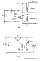
- FIGS. 1a, 1b, 1c, and 1d show a synchronizing pulse of a video signal with SIS pulses shown in simplified form inserted in the synchronizing pulse.
- the voltage level of the synchronous pulse floor is designated U s .
- the line streaking which arises as a result of the different voltage levels U x of the SIS pulses can be represented, for example, by two successive synchronous pulses at times t 1 and t 2 , the pulse floors being smooth, but at a different voltage level U.
- S1 and U S2 are located, as shown by the voltage curve in front of the clamping capacitor C1 in FIG. 1b, corresponding to U 1 in FIG. 1c.
- the difference between the voltage levels U S1 and U S2 is ⁇ U S.
- the clamping voltage U O shown in FIG. 1b then results in the voltages U C11 and U C12 at the clamping capacitor C1.
- a video signal is assumed in Fig. 1b for further clarification of the resulting SIS line interference, the image content for the two lines shown corresponds to the white value W, so that the signal representing the image content before and after the synchronizing pulses is at the same voltage level.
- the object of the invention is a method for recovering the average image brightness of video signals to be raised, which largely prevents the occurrence of line interference even when inserting high-frequency pulse trains into the synchronizing pulses and which is nevertheless universally applicable to all television standards.
- the object is achieved in that when high-frequency pulse sequences are inserted into the synchronizing pulses, the potential fluctuations in the bottoms of these high-frequency pulse sequences are retained during clamping, so that these different potential values are not converted into amplitude fluctuations in the mean line level of the video signal.
- a circuit arrangement for performing the method is specified in claim 2.
- the SIS signal-to-noise ratio When using the invention, the SIS signal-to-noise ratio, with the same hum tolerance as in conventional circuits (0.7 V SS - 50 Hz), is increased to such an extent that line streaking can no longer be recognized in a normally set television picture, which is the case with signal-to-noise ratios according to the invention is greater than 50 dB.
- the switch S can be implemented, for example, by a transistor be.
- the resistance R i is the internal resistance of the following amplifier.
- the switch S is closed and the voltage U 1 is embodied by the synchronous pulse level U S.
- the pulse floor level U 2 for the clamped signal then results in U 2 - U O.
- the switch S is open. Because of the internal resistance R i of the amplifier, point b then becomes more negative than point a.
- the DC voltage at point a remains constant.
- the point b of the capacitor C1 (FIG. 2) is always kept at a constant potential during the clamping process, while at the point a the SIS signal is present, so that the charge of C1 depends on the SIS content of the SIS pulses inserted in the synchronous pulse.
- This dependence of the voltage U 0 is implemented in practice by inserting the resistor R10 in series with the voltage source U O with the internal resistance O ⁇ (see Fig. 5).
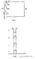
- the basic circuit diagram of the original clamp circuit corresponding to Fig.2 is shown in Fig.4.
- the signal curve U 1 at the input and the corresponding clamping pulse curve U K at the base of the transistor T1 are also shown there.
- the generation of the clamping pulses will be discussed later.
- FIG. 7 shows in detail a circuit arrangement for carrying out the method according to the invention.
- This circuit arrangement consists of the switching stage S1, the Ver stronger V and the pulse shaper stage P.
- the amplifier V is designed here, for example, as a multi-stage transistor amplifier with a high-resistance input, as shown in FIG. 3 of DE-PS 1 809 362.
- the switching stage S1 at the input of which the video signal U 1 is present, consists of the clamping transistor T1, the clamping capacitor C1, the voltage divider R11 / R12, the capacitor C7, the resistor R10 and the diode D1.
- the voltage source U O shown in FIG. 5 with the internal resistance O ⁇ is realized here by means of the voltage divider R11 / R12 and the capacitor C7.
- C7 is charged via R10 to the voltage determined by R11 / R12 during a line, that is to say in the time between two horizontal synchronizing pulses (H pulses) when transistor T1 is blocked.
- R12 has a high resistance to R10 and C7 is much larger than C1 in terms of capacitance (eg C7 - 220 uF and C1 - 0.047 ⁇ F)
- C7 acts as a voltage source with the internal resistance O ⁇ when transistor T1 is switched on.
- the function of the resistor R10 connected in series with the voltage source has already been explained with reference to FIG.
- R10-200 ⁇ , R12-3.3 kQ and R11-400Q To compensate for temperature-related fluctuations in SIS line interference, R10 can be designed as a 200 ⁇ thermistor.
- the pulse shaper stage P with the transistor T5 serves to generate the clamping pulses for the switching stage S1 and is galvanically coupled to the output of the amplifier V.
- the polarized terminal pulses are picked up at the collector of the transistor T5 and fed to the base of the switching transistor T1 via the RC element C4 / R7 and the coupling capacitor C5.
- the collector resistor R4 is not bridged here with a capacitor C3 as in FIG. 3 of DE-PS 1 809 362 in order to prevent a delay in the rise time of the clamping pulses and thus to enable a time-synchronous clamping to the SIS pulses.
- the resultant relationships are shown in FIG. 8 on the basis of a synchronizing pulse not afflicted with SIS pulses.
- FIG. 8a shows a synchronous pulse of the video signal and FIG. 8b shows the clamping pulse occurring at the collector of T5 when capacitor C3 is present.
- the clamping pulse occurring at the base of T1 is then shown in FIG. 8c, the pulse-distributing effect of the RC element C4 / R7 being visible.
- Figure 8D shows the finally Klemmim p uls at the base of C1 without the capacitor C3.
- the amplification of the pulse shaping stage formed with T5 is set by means of the variable resistor R13 so that the Clamping pulses receive the amplitude with which on the one hand there is still the possibility of superimposing 0.7 V SS - 50 Hz hum and on the other hand the transfer of C1 through the thereby defined, softer switching of T1 takes place in such a way that there are no streaks or beeping beeps are visible in the synchronous pulse edges.
- the diode D1 arranged in the switching stage S1 between the emitter and the collector of the transistor T1 serves to initiate the clamping process, since this would otherwise not start at low voltages of the video signal. Because of the lack of charge on capacitor C1, the amplifier would be blocked, so that no clamping pulses could arise which would bring this charge to C1 the. If the actual clamping circuit works once, is. the diode D1 has no effect since it is permanently blocked.
- the choke coil with damping pearl L1 inserted in the emitter line of T5 in the pulse shaping stage P causes a gain loss in the pulse shaping stage for the high-frequency pulse components c of the SIS pulses.
- the absolute value of the SIS interference cannot be reduced, but the clamping pulse shaping thus brought about causes a clearly visible calming effect of the SIS interference which may still be visible in a television picture, the actual video signal not experiencing any recognizable changes.
- the temperature response of transistor T5 is compensated for by diode D2.
- the collector voltage of T5 is limited with the aid of the diode D3, the Zener diode D4 and the resistor R6.
- the diode D5 becomes temporarily transparent, as a result of which the voltage of the capacitor C7 is changed in rhythm with the color oscillation (approx. 2.4 MHz), since a capacitor of the order of magnitude like C7, which, for example, consists of a 220 ⁇ F tantalum electrolvt capacitor, does not approximate a short circuit due to its series inductance for these frequencies.
- the transistor T1 thus switches through at the peaks of the color oscillation, but the voltage with which it charges the capacitor C1 does not correspond to the voltage value of the sync pulse floor level, but is reduced due to the effect of the diode D5 which is switched through.
- the negative color vibration peaks are clamped, but with appropriate dimensioning of the resistor R14 (for example 250 ⁇ ), it is precisely at such a level that there is no shift in the potential of the image content.
- the resistance diode element D5 / R14 thus supports the effect of the resistance R10 according to the principle of the voltage source U O carried along. The gradation between synchronimouls level and color vibration level is retained. With R10 alone, image errors due to such serious voltage differences between the sync pulse level and the color vibration level could not be avoided.
Landscapes
- Engineering & Computer Science (AREA)
- Multimedia (AREA)
- Signal Processing (AREA)
- Picture Signal Circuits (AREA)
Abstract
Description
Die Erfindung betrifft ein Verfahren zur Wiedergewinnung der mittleren Bildhelligkeit eines Videosignals und zur Beseitigung von dem Videosignal überlagerten niederfrequenten Störspannungen, wobei auf das Niveau der jeweiligen Synchronimpulsböden geklemmt wird.The invention relates to a method for recovering the average image brightness of a video signal and for eliminating low-frequency interference voltages superimposed on the video signal, clamping to the level of the respective sync pulse bases.
Bei Übertragungsstrecken; die das Videosignal amplitudenmoduliert übertragen, ist es üblich, vor dem Modulator die mittlere Bildhelligkeit wiederzugewinnen, um die Aussteuerung der Leitungsverstärker möglichst klein zu halten und um niederfrequente Störspannungen des angelieferten Videosignals zu beseitigen.For transmission links; which transmit the video signal with amplitude modulation, it is customary to regain the average image brightness in front of the modulator in order to keep the modulation of the line amplifiers as small as possible and to eliminate low-frequency interference voltages of the supplied video signal.
Bei solchen Klemmschaltungen gelangt das Videosignal über einen Vorverstärker an einen Klemmkondensator. Dieser wird während der Dauer der Synchronimpulse jeweils mittels eines Schalters (z.B. Schalttransistor) auf eine den Arbeitspunkt des nachfolgenden Verstärkers festlegende Spannung umgeladen (Klemmprinzip).In such clamping circuits, the video signal reaches a clamping capacitor via a preamplifier. During the duration of the sync pulses, this is reloaded by means of a switch (e.g. switching transistor) to a voltage that defines the operating point of the subsequent amplifier (clamping principle).
Bisher bekannte Klemmschaltungen, wie sie z.B. in der DE-PS 1 809 362 angeführt werden, verursachen nur dann keinerlei in einem Fernsehbild sichtbare Störungen, wenn die Impulsböden, auf welche geklemmt wird, einen hochfrequenzmäßig möglichst glatten Verlauf haben. Werden in die Synchronimpulse hochfrequente Impulsfolgen, beispielsweise nach dem PCM-Verfahren zur gleichzeitigen Übertragung des Tonsignals mit dem Videosignal (Sound-in-Synch- oder SIS-Verfahren), eingefügt, verursachen diese Klemmschaltungen Bildstörungen. Diese als Zeilenstreifigkeit bezeichnete Bildstörungen ergeben sich dadurch, daß erstens die Impulsböden der PCM-Imoulse im ursorünglichen, ungeklemmten Zustand nicht alle auf gleichem Spannungsniveau sind und daß zweitens die Anzahl der in einem Synchronimouls enthaltenen PCM-Impulse von Synchronimpuls zu Svnchronimpuls, abhängig vom Tonsignal, schwankt. Da nach dem Klemmvorgang die PCM-Impulsböden bei den bisher bekannten Klemmschaltungen auf ein gemeinsames, konstantes Spannungsniveau geklemmt werden, und außerdem die am Klemmkondensator auftretende Ladungsänderung abhängig ist von der Klemmdauer, d.h. bei SIS-Signalen abhängig von der Dauer der PCM-Impulsböden bzw. von der Anzahl der Impulsböden ist, ergibt sich bei SIS-Signalen eine Abhängigkeit des mittleren Zeilenniveaus vom PCM-Signalinhalt.Previously known clamp circuits, such as those mentioned in DE-PS 1 809 362, cause only then no disturbances visible in a television picture if the pulse floors to which they are clamped are as smooth as possible in terms of radio frequency. If high-frequency pulse sequences are inserted into the synchronizing pulses, for example according to the PCM method for the simultaneous transmission of the audio signal with the video signal (sound-in-synch or SIS method), these clamping circuits cause image interference. These image disturbances, known as line streaking, result from the fact that, firstly, the pulse bottoms of the PCM imoulse in the original, unclamped state are not all at the same voltage level, and secondly that the number of PCM pulses contained in one synchronimouls from synchronous pulse to synchronous pulse, depending on the sound signal, fluctuates. Since after the clamping process the PCM pulse plates are clamped to a common, constant voltage level in the previously known clamping circuits, and also the charge change occurring at the clamping capacitor is dependent on the clamping duration, ie in the case of SIS signals, on the duration of the PCM pulse plates or on the number of pulse bases, SIS signals are dependent on the mean line level on the PCM signal content.
Mit solchen Klemmschaltungen entstehen bei einem Videosignal von 1 VSS (entsprechend etwa 0,7 VSS Bildinhalt) Amplituden der SIS-Zeilenstörungen von ca. 15 mV, was einem Störabstand von etwa 33 dB entspricht. Dem Videosignal darf hierbei eine 50 Hz - Brummsoannung von maximal ca. 0,7 VSS überlagert sein, ohne daß ein Ausset- zen der Klemmung erfolgt. Die Brummunterdrückung beträgt ca. 26 dB ohne SIS-Impulse in den Svnchronimpulsen, mit SIS-Impulsen ca. 20 dB.With such clamp circuits, for a video signal of 1 V SS (corresponding to approximately 0.7 V SS image content), amplitudes of the SIS line interference of approximately 15 mV arise, which corresponds to a signal-to-noise ratio of approximately 33 dB. The video signal may in this case a 50 Hz - be superimposed Brummsoannung of a maximum of about 0.7 V SS without a Ausset - zen the clamping is carried out. The hum suppression is approx. 26 dB without SIS impulses in the synchronizing impulses, with SIS impulses approx. 20 dB.
Die Entstehung von Zeilenstörungen wird anhand der Figuren 1a, 1b, 1c, und 1d veranschaulicht. Fig. 1a zeigt einen Synchronimpuls eines Videosignals mit vereinfacht dargestellten in den Synchronimpuls eingefügten SIS-Impulsen. Das Spannungsniveau des Synchronimpulsbodens ist mit Us bezeichnet.Die infolge der unterschiedlichen Spannungsniveaus Ux der SIS-Impulse entstehende Zeilenstreifigkeit kann z.B. durch zwei aufeinanderfolgende Synchronimpulse zur Zeit t1 und t2 dargestellt werden, wobei die Impulsböden glatt sind, jedoch auf unterschiedlichem Spannungsniveau US1 bzw. US2 liegen, wie dies der in Fig.lb dargestellte Spannungsverlauf vor dem Klemmkondensator C1, entsprechend U1 in Fig,1c, zeigt. Der Unterschied zwischen den Spannungsniveaus US1 und US2 ist ΔUS. Mit der in Fig.1b eingezeichneten Klemmspannung UO ergeben sich dann die Spannungen UC11 bzw. UC12 am Klemmkondensator C1. Außerdem ist in Fig. 1b zur weiteren Verdeutlichung der entstehenden SIS-Zeilenstörung ein Videosignal angenommen, dessen Bildinhalt für die zwei dargestellten Zeilen dem Weißwert W entspricht, so daß das den Bildinhalt darstellende Signal vor und hinter den Synchronimpulsen auf gleichem Spannungsniveau liegt.The formation of line faults is illustrated with the aid of FIGS. 1a, 1b, 1c, and 1d. Fig. 1a shows a synchronizing pulse of a video signal with SIS pulses shown in simplified form inserted in the synchronizing pulse. The voltage level of the synchronous pulse floor is designated U s . The line streaking which arises as a result of the different voltage levels U x of the SIS pulses can be represented, for example, by two successive synchronous pulses at times t 1 and t 2 , the pulse floors being smooth, but at a different voltage level U. S1 and U S2 are located, as shown by the voltage curve in front of the clamping capacitor C1 in FIG. 1b, corresponding to U 1 in FIG. 1c. The difference between the voltage levels U S1 and U S2 is ΔU S. The clamping voltage U O shown in FIG. 1b then results in the voltages U C11 and U C12 at the clamping capacitor C1. In addition, a video signal is assumed in Fig. 1b for further clarification of the resulting SIS line interference, the image content for the two lines shown corresponds to the white value W, so that the signal representing the image content before and after the synchronizing pulses is at the same voltage level.
Das Spannungsniveau U2 für die Impulsböden nach dem Klemmkondensator C1 ergibt sich nach erfolgtem Klemmvorgang gemäß Fig.1c allgemein zu:![]()
![]()
![]()
![]()
Aufgabe der Erfindung ist es, ein Verfahren zur Wiedergewinnung der mittleren Bildhelligkeit von Videosignalen anzuheben, das auch beim Einfügen hochfrequenter Impulsfolgen in die Synchronimpulse die Entstehung von Zeilenstörungen weitestgehend verhindert und das trotzdem bei allen Fernsehnormen universell anwendbar ist.The object of the invention is a method for recovering the average image brightness of video signals to be raised, which largely prevents the occurrence of line interference even when inserting high-frequency pulse trains into the synchronizing pulses and which is nevertheless universally applicable to all television standards.
Die Aufgabe wird erfindungsgemäß dadurch gelöst, daß bei Einfügung hochfrequenter Impulsfolgen in die Synchronimpulse die Potentialschwankungen in den Imnulsböden dieser hochfrequenten Impulsfolgen bei der Klemmung erhalten bleiben, so daß diese unterschiedlichen Potentialwerte nicht in Amplitudenschwankungen des mittleren Zeilenniveaus des Videosignals umgesetzt werden.The object is achieved in that when high-frequency pulse sequences are inserted into the synchronizing pulses, the potential fluctuations in the bottoms of these high-frequency pulse sequences are retained during clamping, so that these different potential values are not converted into amplitude fluctuations in the mean line level of the video signal.
Eine Schaltungsanordnung zur Durchführung des Verfahrens ist im Anspruch 2 angegeben.A circuit arrangement for performing the method is specified in
Bei Anwendung der Erfindung wird der SIS-Störabstand, bei gleicher Brummverträglichkeit wie bei herkömmlichen Schaltungen (0,7 VSS - 50 Hz), so weit erhöht, daß eine Zeilenstreifigkeit in einem normal eingestellten Fernsehbild nicht mehr zu erkennen ist, was erfindungsgemäß bei Störabständen größer 50 dB der Fall ist.When using the invention, the SIS signal-to-noise ratio, with the same hum tolerance as in conventional circuits (0.7 V SS - 50 Hz), is increased to such an extent that line streaking can no longer be recognized in a normally set television picture, which is the case with signal-to-noise ratios according to the invention is greater than 50 dB.
Vorteilhafte Ausgestaltungen sind den übrigen Unteransprüchen entnehmbar.Advantageous refinements can be found in the remaining subclaims.
Anhand der Fig.2 bis 7 wird im folgenden das erfindungsgemäße Verfahren und ein Ausführungsbeispiel einer Schaltungsanordnung zur Durchführung des Verfahrens näher erläutert.The method according to the invention and an exemplary embodiment of a circuit arrangement for carrying out the method are explained in more detail below with reference to FIGS. 2 to 7.
Zum besseren Verständnis werden zunächst anhand des in Fig.2 gezeigten Prinzipschaltbildes die Vorgänge bei bekannten Klemmschaltungen dargestellt. Der Schalter S kann beisoielsweise durch einen Transistor verwirklicht sein. Der Widerstand Ri ist der Innenwiderstand des nachfolgenden Verstärkers. Während der Synchronimoulse ist der Schalter S geschlossen und die Spannung U1 wird durch das Synchronimpulsniveau US verkörpert. Das Impulsbodenniveau U2 für das geklemmte Signal ergibt sich dann zu U2 - UO. Wenn die Spannung U1 den Bildinhalt verkörpert, ist der Schalter S offen. Wegen des Innenwiderstandes Ri des Verstärkers wird dann der Punkt b negativer als der Punkt a. Die Gleichspannung am Punkt a bleibt konstant. Dies bedeutet, daß die Gleichspannung UC1 am Kondensator C1 größer und damit die den Arbeitspunkt bestimmende mittlere Gleichspannung U2 kleiner wird (vgl.Fig.1c). Der Klemmvorgang bewirkt nun, daß C1 mittels der Spannungsquelle UO wieder auf den ursprünglichen, dem Synchronimpulsniveau:zugeordneten Spannungswert entladen wird, wobei dann ein Strom IK mit der in Fig.2 eingezeichneten Richtung fließt, wodurch von Zeile zu Zeile der Arbeitspunkt des nachfolgenden Verstärkers wiederhergestellt wird. Durch diese Wiederherstellung des Arbeitspunktes werden auch der Signalspannung U1 überlagerte niederfrequente Störspannungen, deren Frequenz klein ist gegenüber der Wiederholfrequenz der Synchronimpulse, beseitigt.For a better understanding, the processes in known clamping circuits are first shown on the basis of the basic circuit diagram shown in FIG. The switch S can be implemented, for example, by a transistor be. The resistance R i is the internal resistance of the following amplifier. During the synchronous pulse, the switch S is closed and the voltage U 1 is embodied by the synchronous pulse level U S. The pulse floor level U 2 for the clamped signal then results in U 2 - U O. When the voltage U 1 embodies the image content, the switch S is open. Because of the internal resistance R i of the amplifier, point b then becomes more negative than point a. The DC voltage at point a remains constant. This means that the DC voltage U C1 on the capacitor C1 is larger and thus the mean DC voltage U 2 determining the operating point becomes smaller (see Fig. 1c). The clamping process now causes C1 to be discharged again to the original voltage value assigned to the sync pulse level: by means of the voltage source U O , a current I K then flowing in the direction shown in FIG. 2, which means that the operating point of the subsequent line flows from line to line Amplifier is restored. This restoration of the operating point also eliminates the low-voltage interference voltages superimposed on the signal voltage U 1 , the frequency of which is low compared to the repetition frequency of the synchronizing pulses.
Wird nun, wie beispielsweise in der DE-PS 1 809 362, eine Spannungsquelle UO mit dem Innenwiderstand OΩ benutzt, so wird der Punkt b des Kondensators C1 (Fig.2) stets auf konstantem Potential zu Zeiten des Klemmvorgangs gehalten, während am Punkt a das SIS-Signal anliegt, wodurch die Ladung von C1 vom SIS-Inhalt der in den Svnchronimpuls eingefügten SIS-Impulse abhängig ist.If, as for example in
Der Erfindung liegt nun der Gedanke zugrunde, die Umladung des Kondensators C1 derart zu gestalten, daß die Spannung UC1 unabhängig vom SIS-Inhalt nach jedem Klemmvorgang konstant ist. Von Fig.1b ausgehend erhält man dann für das geklemmte Signal unter der Voraussetzung UC11 = UC12 = UC1 den in Fig.3 dargestellten Verlauf. Die Impulsniveaus US1 und US2 vor der Klemmung sind gestrichelt eingezeichnet. Für die Impulsniveaus nach der Klemmung der beiden dargestellten Impulse erhält man dann:![]()
![]()
![]()
![]()
Die praktische Realisierung dieser Abhängigkeit der Spannung U0 erfolgt durch die Einfügung des Widerstandes R10 in Serie zur Spannungsquelle UO mit dem Innenwiderstand OΩ(vgl.Fig.5).This dependence of the voltage U 0 is implemented in practice by inserting the resistor R10 in series with the voltage source U O with the internal resistance OΩ (see Fig. 5).
Das Prinzipschaltbild der ursprünglichen Klemmschaltung entsnrechend Fig.2 ist in Fig.4 dargestellt. Außerdem ist dort der Signalverlauf U1 am Eingang und der entsprechende Klemmimpulsverlauf UK an der Basis des Transistors T1 dargestellt. Auf die Erzeugung der Klemmimpulse wird soäter eingegangen. Der Klemmtransistor T1 in Fig.4 arbeitet ohne Emittergegenkopolung. Bei dem zur Zeit t2 auftretenden längeren Impuls, d.h. mit niedrigerem Potential des Impulsbodens, wird der Transistor T1 besser durchgeschaltet als bei dem zur Zeit t1 auftretenden kürzeren Impuls, da das Emitterpotential von T1 gleich der Spannung UO = const. ist. Dies begünstigt noch zusätzlich die Entstehung von SIS-Störungen, da zur Zeit t2 die Seite b des Kondensators C1 besser auf das Potential Uo gebracht wird als zur Zeit t1. Das bedeutet, daß UC1 zur Zeit t2 (vgl. UC12 in Fig.lb) infolge der besseren Durchschaltung noch stärker kleiner wird als zur Zeit t1.The basic circuit diagram of the original clamp circuit corresponding to Fig.2 is shown in Fig.4. The signal curve U 1 at the input and the corresponding clamping pulse curve U K at the base of the transistor T1 are also shown there. The generation of the clamping pulses will be discussed later. The clamping transistor T1 in FIG. 4 works without negative emitter feedback. With the longer pulse occurring at time t 2 , ie with a lower potential of the pulse base, the transistor T1 is switched through better than with the shorter pulse occurring at time t 1 , since the emitter potential of T1 is equal to the voltage U O = const. is. This also favors the development of SIS disorders because Time t 2 brings the side b of the capacitor C1 to the potential U o better than at time t 1 . This means that U C1 at time t 2 (v g l. U C12 in Fi g. Lb) becomes even smaller as a result of the better switching through than at time t 1 .
In Fig.5 ist die Prinzipschaltung mit eingefügtem Widerstand R10 dargestellt. An diesem Widerstand fällt die Spannung![]()
![]()
![]()
![]()
Bei größerem UK, d.h. bei positiverem Klemmimpuls zur Zeit t2 an der Basis von T1 wird zunächst der Transistor T1 ebenfalls besser durchgesteuert, wodurch gegenüber dem Zeitpunkt t1 jetzt ein größerer Strom I fließt (IK2 > IK1). Hierdurch entsteht an R10 zur Zeit t2 ein größerer Spannungsabfall, so daß UO zur Zeit t2 kleiner ist als zur Zeit t1 (UO2 < UO1).With a larger U K , ie with a more positive clamping pulse at the time t 2 at the base of T1, the transistor T1 is first also turned on better, as a result of which a larger current I now flows than the time t 1 (I K2 > I K1 ). This creates a larger voltage drop across R 10 at time t 2 , so that U O at time t 2 is smaller than at time t 1 (U O2 <U O1 ).
Dies bewirkt ein zusätzlich besseres Durchschalten von T1 zur Zeit t2, da das UO entsprechende Emitterpotential von T1 sinkt bzw. die für die Durchsteuerung von T1 maßgebende Basis-Emitter-Spannung UBE um den Wert UR10 = R10 . IK steigt.This results in an additional better switching through of T1 at time t 2 , since the U O corresponding emitter potential of T1 drops or the base-emitter voltage U BE decisive for the control of T1 by the value U R10 = R10. I K rises.
Diese Verhältnisse sind in.Fig.6 dargestellt. Für die Durchschaltespannung UBE des Transistors T1 gilt:![]()
![]()
Bei den sich einstellenden Gleichgesaichtszuständen ergibt sich bei entsprechender Dimensionierung von R10 der in Fig.3 dargestellte und angestrebte Zustand UO1> UO2 .In the case of the equilateral states that arise, with appropriate dimensioning of R10, the state U O1 > U O2 shown and desired in FIG. 3 results.
Fig.7 zeigt im Detail eine Schaltungsanordnung zur Durchführung des erfindungsgemäßen Verfahrens. Diese Schaltungsanordnung besteht aus der Schaltstufe S1, dem Verstärker V und der Pulsformerstufe P. Der Verstärker V ist hier beispielsweise als mehrstufiger Trensistorverstärker mit hochohmigen Eingang ausgelegt, wie in Fig.3 der DE-PS 1 809 362 gezeigt.7 shows in detail a circuit arrangement for carrying out the method according to the invention. This circuit arrangement consists of the switching stage S1, the Ver stronger V and the pulse shaper stage P. The amplifier V is designed here, for example, as a multi-stage transistor amplifier with a high-resistance input, as shown in FIG. 3 of
Die Schaltstufe S1, an deren Eingang das Videosignal U1 anliegt, besteht aus dem Klemmtransistor T1, dem Klemmkondensator C1, dem Spannungsteiler R11/R12, dem Kondensator C7, dem Widerstand R10 und der Diode D1. Die in Fig.5 dargestellte Spannungsquelle UO mit dem Innenwiderstand OΩ wird hier mittels des Spannungsteilers R11/R12 und des Kondensators C7 realisiert. C7 wird während einer Zeile, d.h. in der Zeit zwischen zwei Horizontal-Synchronimpulsen (H-Impulsen) bei gesperrtem Transistor T1, über R10 auf die durch R11/R12 bestimmte Spannung aufgeladen. Da R12 hochohmig gegenüber R10 ist und C7 kapazitätsmäßig sehr viel größer als C1 ist (z.B. C7 - 220 uF und C1 - 0,047 µF), wirkt C7 bei durchgeschaltetem Transistor T1 als Spannungsquelle mit dem Innenwiderstand OΩ. Die Funktion des der Spannungsquelle in Serie geschalteten Widerstandes R10 wurde bereits anhand der Fig.5 erläutert. In einer ausgeführten Schaltung ist beispielsweise R10 - 200 Ω, R12 - 3,3 kQ und R11 - 400Q. Um temperaturbedingte Schwankungen der SIS-Zeilenstörungen zu kompensieren, kann R10 als 200 Ω - Heißleiter ausgebildet sein.The switching stage S1, at the input of which the video signal U 1 is present, consists of the clamping transistor T1, the clamping capacitor C1, the voltage divider R11 / R12, the capacitor C7, the resistor R10 and the diode D1. The voltage source U O shown in FIG. 5 with the internal resistance OΩ is realized here by means of the voltage divider R11 / R12 and the capacitor C7. C7 is charged via R10 to the voltage determined by R11 / R12 during a line, that is to say in the time between two horizontal synchronizing pulses (H pulses) when transistor T1 is blocked. Since R12 has a high resistance to R10 and C7 is much larger than C1 in terms of capacitance (eg C7 - 220 uF and C1 - 0.047 µF), C7 acts as a voltage source with the internal resistance OΩ when transistor T1 is switched on. The function of the resistor R10 connected in series with the voltage source has already been explained with reference to FIG. In an implemented circuit, for example, R10-200 Ω, R12-3.3 kQ and R11-400Q. To compensate for temperature-related fluctuations in SIS line interference, R10 can be designed as a 200 Ω thermistor.
Die Pulsformerstufe P mit dem Transistor T5 dient zur Erzeugung der Klemmimpulse für die Schaltstufe S1 und ist galvanisch an den Ausgang des Verstärkers V angekoppelt. Am Kollektor des Transistors T5 werden die umgepolten Klemmimpulse abgegriffen und über das RC-Glied C4/R7 und den Koppelkondensator C5 an die Basis des Schalttransistors T1 geführt. Der Kollektorwiderstand R4 ist hier nicht wie in Fig.3 der DE-PS 1 809 362 mit einem Kondensator C3 überbrückt, um eine Verzögerung der Anstiegszeit der Klemmimpulse zu verhindern und somit eine zu den SIS-Impulsen zeitsynchrone Klemmung zu ermöglichen. Die sich ergebenden Verhältnisse sind in Fig.8 anhand eines nicht mit SIS-Impulsen behafteten Synchronimpulses dargestellt. Fig.8a zeigt einen Synchronimpuls des Videosignals und Fig.8b den am Kollektor von T5 auftretenden Klemmimpuls bei vorhandenem Kondensator C3. In Fig.8c ist dann der an der Basis von T1 auftretende Klemmimpuls dargestellt, wobei die impulsversteilernde Wirkung des RC-Gliedes C4/R7 sichtbar ist. Fig.8d zeigt schließlich den Klemmimpuls an der Basis von C1 ohne den Kondensator C3. Infolge des fehlenden Kondensators C3 tritt eine Impulsformung nun nicht mehr ein, was im Hinblick auf eine möglichst zeitsynchrone Klemmung auf die eine relativ hohe Wiederholfrequenz aufzuweisenden SIS-Impulse erwünscht ist.The pulse shaper stage P with the transistor T5 serves to generate the clamping pulses for the switching stage S1 and is galvanically coupled to the output of the amplifier V. The polarized terminal pulses are picked up at the collector of the transistor T5 and fed to the base of the switching transistor T1 via the RC element C4 / R7 and the coupling capacitor C5. The collector resistor R4 is not bridged here with a capacitor C3 as in FIG. 3 of
Um aber zu vermeiden, daß durch den zeitsynchron zu dem Synchronimpuls des Signals erscheinenden Klemmimpuls (Fig.8d) Signalverfälschungen.in den Synchronimpulsflanken durch zu frühe Klemmung auftreten, wird die Verstärkung der mit T5 gebildeten Pulsformerstufe mittels des veränderbaren Widerstandes R13 so eingestellt, daß die Klemmimpulse die Amplitude erhalten, mit der einerseits die Möglichkeit der Überlagerung von 0,7 VSS - 50 Hz - Brumm noch gegeben ist und andererseits die Umladung von C1 durch das hierdurch festgelegte, weichere Durchschalten von T1 so vor sich geht, daß gerade keine Schlieren bzw. Klemmpiepse in den Synchrönimpulsflanken sichtbar werden.However, in order to avoid signal falsifications occurring in the synchronizing pulse edges due to early clamping due to the clamping pulse (FIG. 8d) appearing synchronously with the synchronizing pulse of the signal, the amplification of the pulse shaping stage formed with T5 is set by means of the variable resistor R13 so that the Clamping pulses receive the amplitude with which on the one hand there is still the possibility of superimposing 0.7 V SS - 50 Hz hum and on the other hand the transfer of C1 through the thereby defined, softer switching of T1 takes place in such a way that there are no streaks or beeping beeps are visible in the synchronous pulse edges.
Die in der Schaltstufe S1 zwischen Emitter und Kollektor des Transistors T1 angeordnete Diode D1 dient zur Einleitung des Klemmvorgangs, da dieser bei kleinen Spannungen des Videosignals sonst nicht in Gang kommen würde. Wegen der fehlenden Ladung auf dem Kondensator C1 wäre der Verstärker gesperrt, so daß auch keine Klemmimpulse entstehen könnten, die diese Ladung auf C1 bringen würden. Arbeitet die eigentliche Klemmschaltung einmal, ist. die Diode D1 wirkungslos, da sie dauernd gesperrt ist. Die in die Emitterleitung von T5 in der Pulsformerstufe P eingefügte Drosselspule mit Dämpfungsperle L1 bewirkt einen Verstärkungsverlust der Pulsformerstufe für die hochfrequenten Impulsanteilc der SIS-Impulse. Das zwischen dcm Bezugspotential 0, dem Kollektor und der Basis von T5 eingefügte T-Glied, bestehend aus den Widerständen R8 und R9, der Induktivität L2 und der Querkapazität C6, verursacht durch seine Tiefpasscharakteristik eine Eigengegenkopnlung der Pulsformerstufe für niederfrequente Impulsanteile der SIS-Impulse. Mit diesen beiden Maßnahmen läßt sich zwar der Absolutwert der SIS-Störungen nicht verringern, jedoch tritt durch die so bewirkte Klemmimpulsformung ein deutlich sichtbarer Beruhigungseffekt der in einem Fernsehbild eventuell noch sichtbaren SIS-Störungen auf, wobei das eigentliche Videosignal keinerlei erkennbare Veränderungen erfährt. Man erhält praktisch zusätzlich einen geglätteten Verlauf.der noch mit einem Abstand von ca. 50 dB vorhandenen SIS-Störungen, das dann von Bedeutung ist, wenn auf einer Video- übertragungsstrecke mehr als eine Klemmschaltung eingesetzt wird, da das Auge die dann noch vorhandenen Störungen mit geglättetem Verlauf als weniger stark empfindet.The diode D1 arranged in the switching stage S1 between the emitter and the collector of the transistor T1 serves to initiate the clamping process, since this would otherwise not start at low voltages of the video signal. Because of the lack of charge on capacitor C1, the amplifier would be blocked, so that no clamping pulses could arise which would bring this charge to C1 the. If the actual clamping circuit works once, is. the diode D1 has no effect since it is permanently blocked. The choke coil with damping pearl L1 inserted in the emitter line of T5 in the pulse shaping stage P causes a gain loss in the pulse shaping stage for the high-frequency pulse components c of the SIS pulses. The T-element inserted between dcm reference potential 0, the collector and the base of T5, consisting of the resistors R8 and R9, the inductance L2 and the transverse capacitance C6, causes a self-negative feedback of the pulse shaper stage for low-frequency pulse components of the SIS pulses due to its low-pass characteristic. With these two measures, the absolute value of the SIS interference cannot be reduced, but the clamping pulse shaping thus brought about causes a clearly visible calming effect of the SIS interference which may still be visible in a television picture, the actual video signal not experiencing any recognizable changes. In practice you also get a smoothed curve of the SIS interference that is still present at a distance of approx. 50 dB, which is important if more than one clamping circuit is used on a video transmission link, since the eye then sees the interference that is still present felt with a smoothed course as less strong.
Der Temperaturgang des Transistors T5 wird durch die Diode D2 kompensiert. Um zu verhindern, daß der Transistor T5 während des Bildinhaltes in die Sättigung gesteuert wird und damit das Signal im Hauptweg verzerrt, wird die Kollektorspannung von T5 mit Hilfe der Diode D3, der Z-Diode D4 und des Widerstandes R6 begrenzt.The temperature response of transistor T5 is compensated for by diode D2. In order to prevent the transistor T5 from being driven into saturation during the image content and thus distorting the signal in the main path, the collector voltage of T5 is limited with the aid of the diode D3, the Zener diode D4 and the resistor R6.
Bei manchen Testbildern, wie z.B. im Dillberg-Testbild, ist bei bestimmten Farben eine Übermodulation vorhanden, die bis unter das Synchronimpulsbodenniveau reicht. Um zu vermeiden, daß die Klemmschaltung auf diese Spitzen, die außerhalb der Synchronimpulse auftreten, klemmt und dadurch sehr große Bildfehler verursacht, ist zwischen der Verbindung des Kondensators C7 (Spannungsquelle UO) mit dem Widerstand R10 in der Schaltstufe und dem Emitter des Transistors T5 in der Pulsformerstufe die Serienschaltung einer Diode D5 und eines Widerstandes R14 eingefügt. Bei normalen Synchronimpulsen fließt kein Strom durch die Diode D5, da sich der Potentialunterschied zwischen dem Emitter von T5 und dem Verbindungspunkt zwischen C7 und R10 so einpendelt, daß die Diode D5 gesperrt ist. Tritt eine Farbübermodulation auf, dessen Spitzen bis unterhalb des Synchronimpulsbodenniveaus reichen, wird die Diode D5 vorübergehend durchlässig, wodurch die Spannung des Kondensators C7 im Rhythmus der Farbschwingung (ca. 2,4 MHz) verändert wird, da ein Kondensator von der Größenordnung wie C7, der beispielsweise aus einem 220 µF-Tantal-Elektrolvt-Kondensator besteht, wegen seiner Serieninduktivität für diese Frequenzen auch nicht mehr angenähert einen Kurzschluß darstellt. Der Transistor T1 schaltet also zwar bei den Spitzen der Farbschwingung durch, die Spannung aber, mit welcher diese den Kondensator C1 umlädt, entspricht nicht dem Spannungswert des Synchronimpulsbodenniveaus, sondern ist infolge der Wirkung der durchgeschalteten Diode D5 erniedrigt. Auf diese Weise erfolgt zwar eine Klemmung der negativen Farbschwingungsspitzen, bei entsprechender Dimensionierung des Widerstandes R14 (beispielsweise 250 Ω)aber gerade auf einem solchen Niveau, daß keine Verschiebung des Potentials des Bildinhaltes stattfindet. Das Widerstands-Dioden-Glied D5/R14 unterstützt also in diesem Fall die Wirkung des Widerstandes R10 nach dem Prinzip der mitgeführten Spannungsquelle UO. Die Stufung zwischen Synchronimoulsniveau und Farbschwingungsniveau bleibt erhalten. Allein mit R10 wären Bildfehler infolge solch gravierender Spannungsunterschiede zwischen Synchronimpulsniveau und Farbschwingungsniveau nicht zu vermeiden. Mit dem hier gezeigten Verfahren bzw. der Schaltungsanordnung zur Durchführung dieses Verfahrens ist es also möglich, die Entstehung von SIS-Zeilenstörungen weitestgehend zu verhindern, wobei die unterschiedlichen Amolitudenwerte der PCM-Impulsböden nicht wie bei bisher üblichen Klemmschaltungen in Amplitudenschwankungen des mittleren Zeilenniveaus umgesetzt werden, sondern diese Amplitudenschwankungen in den Synchronimpulsböden erhalten bleiben, wobei dann auf das jeweilige Synchronimpulsbodenniveau geklemmt wird. Diese Tatsache kommt deshalb einer Verminderung der von Klemmschaltungen verursachten Signalverfälschungen gleich. Außerdem sind die Signalverfälschungen für die Vertikal- und Horizontal-Synchronimpulse absolut gesehen geringer als bei den bisherigen Schaltungen. Auch das Zeilenrauschen ist geringer, weil den Synchronimpulsböden überlagerte Rauschspitzen analog wie SIS-Impulsspitzen behandelt werden. Die eingangs aufgeführten Werte für die Brummunterdrückung (ca. 26 dB ohne SIS-Impulse und ca. 20 dB mit SIS-Impulsen) werden ebenfalls erreicht. Durch Klemmung auf die Synchronimpulsböden ist die Erfindung für alle Fernsehnormen geeignet.With some test patterns, such as the Dillberg test pattern, there is overmodulation with certain colors that extends below the sync pulse floor level. To avoid that the clamp circuit on these peaks, the occur outside the sync pulses, jams and causes very large image errors, is the series connection of a diode D5 and a resistor R14 between the connection of the capacitor C7 (voltage source U O ) with the resistor R10 in the switching stage and the emitter of the transistor T5 in the pulse shaper stage inserted. With normal synchronizing pulses, no current flows through the diode D5, since the potential difference between the emitter of T5 and the connection point between C7 and R10 settles in such a way that the diode D5 is blocked. If color overmodulation occurs, the peaks of which reach below the sync pulse floor level, the diode D5 becomes temporarily transparent, as a result of which the voltage of the capacitor C7 is changed in rhythm with the color oscillation (approx. 2.4 MHz), since a capacitor of the order of magnitude like C7, which, for example, consists of a 220 µF tantalum electrolvt capacitor, does not approximate a short circuit due to its series inductance for these frequencies. The transistor T1 thus switches through at the peaks of the color oscillation, but the voltage with which it charges the capacitor C1 does not correspond to the voltage value of the sync pulse floor level, but is reduced due to the effect of the diode D5 which is switched through. In this way, the negative color vibration peaks are clamped, but with appropriate dimensioning of the resistor R14 (for example 250 Ω), it is precisely at such a level that there is no shift in the potential of the image content. In this case, the resistance diode element D5 / R14 thus supports the effect of the resistance R10 according to the principle of the voltage source U O carried along. The gradation between synchronimouls level and color vibration level is retained. With R10 alone, image errors due to such serious voltage differences between the sync pulse level and the color vibration level could not be avoided. With the method shown here or the circuit arrangement for carrying out this method, it is thus possible to largely prevent the occurrence of SIS line disturbances, the different amolite values of the PCM pulse plates not being converted into amplitude fluctuations in the mean line level, as was the case with conventional clamping circuits to date, but these amplitude fluctuations are retained in the synchronous pulse floors, and then clamping is carried out to the respective synchronous pulse floor level. This fact therefore equates to a reduction in the signal distortions caused by clamping circuits. In addition, the signal distortions for the vertical and horizontal sync pulses are, in absolute terms, less than with the previous circuits. The line noise is also lower because noise peaks superimposed on the sync pulse floors are treated in the same way as SIS pulse peaks. The hum suppression values listed at the beginning (approx. 26 dB without SIS pulses and approx. 20 dB with SIS pulses) are also achieved. By clamping onto the sync pulse bases, the invention is suitable for all television standards.
Claims (6)
Applications Claiming Priority (2)
| Application Number | Priority Date | Filing Date | Title |
|---|---|---|---|
| DE19782811221 DE2811221A1 (en) | 1978-03-15 | 1978-03-15 | METHOD AND CIRCUIT ARRANGEMENT FOR RECOVERING THE AVERAGE BRIGHTNESS OF A VIDEO SIGNAL |
| DE2811221 | 1978-03-15 |
Publications (3)
| Publication Number | Publication Date |
|---|---|
| EP0004083A2 true EP0004083A2 (en) | 1979-09-19 |
| EP0004083A3 EP0004083A3 (en) | 1979-10-31 |
| EP0004083B1 EP0004083B1 (en) | 1982-03-24 |
Family
ID=6034495
Family Applications (1)
| Application Number | Title | Priority Date | Filing Date |
|---|---|---|---|
| EP79100710A Expired EP0004083B1 (en) | 1978-03-15 | 1979-03-09 | Circuit arrangement for restoring the mean picture brightness of a video signal |
Country Status (3)
| Country | Link |
|---|---|
| EP (1) | EP0004083B1 (en) |
| AT (1) | AT374647B (en) |
| DE (2) | DE2811221A1 (en) |
Cited By (3)
| Publication number | Priority date | Publication date | Assignee | Title |
|---|---|---|---|---|
| FR2534398A1 (en) * | 1982-10-06 | 1984-04-13 | Animotion Inc | Resiliently protected reflective road marking stud |
| GB2148636A (en) * | 1983-09-15 | 1985-05-30 | Sinclair Res Ltd | Improvements in or relating to television receivers |
| US4642688A (en) * | 1983-06-24 | 1987-02-10 | Scientific Atlanta, Inc. | Method and apparatus for creating encrypted and decrypted television signals |
Families Citing this family (1)
| Publication number | Priority date | Publication date | Assignee | Title |
|---|---|---|---|---|
| DE3428301A1 (en) * | 1984-08-01 | 1986-02-13 | Philips Patentverwaltung Gmbh, 2000 Hamburg | CIRCUIT ARRANGEMENT FOR GENERATING CLAMP PULSES |
Citations (1)
| Publication number | Priority date | Publication date | Assignee | Title |
|---|---|---|---|---|
| US2863943A (en) * | 1954-11-30 | 1958-12-09 | Rca Corp | Feedback clamping circuit arrangements |
-
1978
- 1978-03-15 DE DE19782811221 patent/DE2811221A1/en not_active Withdrawn
-
1979
- 1979-03-09 DE DE7979100710T patent/DE2962319D1/en not_active Expired
- 1979-03-09 EP EP79100710A patent/EP0004083B1/en not_active Expired
- 1979-03-14 AT AT0191679A patent/AT374647B/en not_active IP Right Cessation
Patent Citations (1)
| Publication number | Priority date | Publication date | Assignee | Title |
|---|---|---|---|---|
| US2863943A (en) * | 1954-11-30 | 1958-12-09 | Rca Corp | Feedback clamping circuit arrangements |
Cited By (3)
| Publication number | Priority date | Publication date | Assignee | Title |
|---|---|---|---|---|
| FR2534398A1 (en) * | 1982-10-06 | 1984-04-13 | Animotion Inc | Resiliently protected reflective road marking stud |
| US4642688A (en) * | 1983-06-24 | 1987-02-10 | Scientific Atlanta, Inc. | Method and apparatus for creating encrypted and decrypted television signals |
| GB2148636A (en) * | 1983-09-15 | 1985-05-30 | Sinclair Res Ltd | Improvements in or relating to television receivers |
Also Published As
| Publication number | Publication date |
|---|---|
| EP0004083B1 (en) | 1982-03-24 |
| ATA191679A (en) | 1983-09-15 |
| AT374647B (en) | 1984-05-10 |
| EP0004083A3 (en) | 1979-10-31 |
| DE2811221A1 (en) | 1979-09-20 |
| DE2962319D1 (en) | 1982-04-29 |
Similar Documents
| Publication | Publication Date | Title |
|---|---|---|
| DE2366526C2 (en) | Synchronous detector for color synchronous signals | |
| DE2819775C3 (en) | Circuit arrangement for automatic beam current limitation of a picture tube | |
| DE2712024A1 (en) | CIRCUIT ARRANGEMENT FOR REGENERATING SYNCHRONOUS SIGNALS | |
| DE2853927A1 (en) | TELEVISION RECEIVER WITH A HORIZONTAL SYNC | |
| DE2815028C2 (en) | Circuit arrangement for television sets for generating a parabolic signal | |
| DE3046460C2 (en) | Modulator circuit for the amplitude modulation of a video signal onto a carrier signal | |
| EP0004083B1 (en) | Circuit arrangement for restoring the mean picture brightness of a video signal | |
| DE2425975C3 (en) | Circuit for obtaining vertical sync signals | |
| DE2158250C3 (en) | Image display device with a line phase discriminator for generating a control voltage | |
| DE2116265B2 (en) | Circuit arrangement for reducing interference and for stabilizing synchronization signals | |
| CH629052A5 (en) | ELECTRONIC TRANSMITTER FOR DC ELECTRICAL SYSTEMS. | |
| DE2166154B2 (en) | Color television receiver with a transistorized vertical deflection circuit | |
| DE2820242A1 (en) | LINE SELECTOR FOR A TV RECEIVER | |
| DE2720665C3 (en) | Sawtooth generator | |
| DE2533599A1 (en) | Vertical deflection circuit for TV receiver - derives precisely shaped and phased blanking pulses from flyback pulses | |
| DE3140060C2 (en) | Color signal processing circuit | |
| DE2931985A1 (en) | CIRCUIT ARRANGEMENT IN A COLOR TV ENCODER | |
| DE3337298C2 (en) | Arrangement for the automatic regulation of the bias of a picture tube | |
| DE2548266B2 (en) | Generator for supplying a television deflection circuit with pulses for the development of deflection signals | |
| DE4239666C2 (en) | Method and circuit arrangement for tangent equalization of vertical deflection circuits for image display devices | |
| DE1038106B (en) | Synchronizing device for television receivers | |
| DE2511089C3 (en) | Circuit for obtaining the vertical pulse from a television synchronization signal | |
| DE2057531C3 (en) | Circuit arrangement for blanking out interference in the case of an information signal | |
| DE2718571A1 (en) | DEFLECTION WITH MEASURES TO SUPPRESS UNWANTED MODULATIONS | |
| DE2356021C3 (en) | Triggerable sawtooth generator with controllable trigger blocking phase |
Legal Events
| Date | Code | Title | Description |
|---|---|---|---|
| PUAI | Public reference made under article 153(3) epc to a published international application that has entered the european phase |
Free format text: ORIGINAL CODE: 0009012 |
|
| PUAL | Search report despatched |
Free format text: ORIGINAL CODE: 0009013 |
|
| AK | Designated contracting states |
Designated state(s): BE CH DE FR GB IT NL |
|
| AK | Designated contracting states |
Designated state(s): BE CH DE FR GB IT NL |
|
| 17P | Request for examination filed | ||
| ITF | It: translation for a ep patent filed |
Owner name: DE DOMINICIS & MAYER S.R.L. |
|
| GRAA | (expected) grant |
Free format text: ORIGINAL CODE: 0009210 |
|
| AK | Designated contracting states |
Designated state(s): BE CH DE FR GB IT NL |
|
| REF | Corresponds to: |
Ref document number: 2962319 Country of ref document: DE Date of ref document: 19820429 |
|
| PGFP | Annual fee paid to national office [announced via postgrant information from national office to epo] |
Ref country code: NL Payment date: 19850331 Year of fee payment: 7 |
|
| PG25 | Lapsed in a contracting state [announced via postgrant information from national office to epo] |
Ref country code: NL Effective date: 19861001 |
|
| NLV4 | Nl: lapsed or anulled due to non-payment of the annual fee | ||
| PGFP | Annual fee paid to national office [announced via postgrant information from national office to epo] |
Ref country code: GB Payment date: 19910301 Year of fee payment: 13 |
|
| PGFP | Annual fee paid to national office [announced via postgrant information from national office to epo] |
Ref country code: BE Payment date: 19910320 Year of fee payment: 13 |
|
| PGFP | Annual fee paid to national office [announced via postgrant information from national office to epo] |
Ref country code: FR Payment date: 19910322 Year of fee payment: 13 |
|
| ITTA | It: last paid annual fee | ||
| PGFP | Annual fee paid to national office [announced via postgrant information from national office to epo] |
Ref country code: DE Payment date: 19910523 Year of fee payment: 13 |
|
| PGFP | Annual fee paid to national office [announced via postgrant information from national office to epo] |
Ref country code: CH Payment date: 19910624 Year of fee payment: 13 |
|
| PG25 | Lapsed in a contracting state [announced via postgrant information from national office to epo] |
Ref country code: GB Effective date: 19920309 |
|
| PG25 | Lapsed in a contracting state [announced via postgrant information from national office to epo] |
Ref country code: CH Effective date: 19920331 Ref country code: BE Effective date: 19920331 |
|
| BERE | Be: lapsed |
Owner name: TEKADE FELTEN & GUILLAUME FERNMELDEANLAGEN G.M.B. Effective date: 19920331 |
|
| GBPC | Gb: european patent ceased through non-payment of renewal fee | ||
| PG25 | Lapsed in a contracting state [announced via postgrant information from national office to epo] |
Ref country code: FR Effective date: 19921130 |
|
| REG | Reference to a national code |
Ref country code: CH Ref legal event code: PL |
|
| PG25 | Lapsed in a contracting state [announced via postgrant information from national office to epo] |
Ref country code: DE Effective date: 19921201 |
|
| REG | Reference to a national code |
Ref country code: FR Ref legal event code: ST |
|
| PLBE | No opposition filed within time limit |
Free format text: ORIGINAL CODE: 0009261 |
|
| STAA | Information on the status of an ep patent application or granted ep patent |
Free format text: STATUS: NO OPPOSITION FILED WITHIN TIME LIMIT |