DE112008002467B4 - Method for the removal of semiconductor chips from a wafer table and the mounting of the semiconductor chips on a substrate - Google Patents
Method for the removal of semiconductor chips from a wafer table and the mounting of the semiconductor chips on a substrate Download PDFInfo
- Publication number
- DE112008002467B4 DE112008002467B4 DE112008002467T DE112008002467T DE112008002467B4 DE 112008002467 B4 DE112008002467 B4 DE 112008002467B4 DE 112008002467 T DE112008002467 T DE 112008002467T DE 112008002467 T DE112008002467 T DE 112008002467T DE 112008002467 B4 DE112008002467 B4 DE 112008002467B4
- Authority
- DE
- Germany
- Prior art keywords
- camera
- coordinate system
- image
- semiconductor chip
- bondhead
- Prior art date
- Legal status (The legal status is an assumption and is not a legal conclusion. Google has not performed a legal analysis and makes no representation as to the accuracy of the status listed.)
- Active
Links
Images

Classifications
-
- H—ELECTRICITY
- H01—ELECTRIC ELEMENTS
- H01L—SEMICONDUCTOR DEVICES NOT COVERED BY CLASS H10
- H01L21/00—Processes or apparatus adapted for the manufacture or treatment of semiconductor or solid state devices or of parts thereof
- H01L21/67—Apparatus specially adapted for handling semiconductor or electric solid state devices during manufacture or treatment thereof; Apparatus specially adapted for handling wafers during manufacture or treatment of semiconductor or electric solid state devices or components ; Apparatus not specifically provided for elsewhere
- H01L21/67005—Apparatus not specifically provided for elsewhere
- H01L21/67011—Apparatus for manufacture or treatment
- H01L21/67144—Apparatus for mounting on conductive members, e.g. leadframes or conductors on insulating substrates
-
- H—ELECTRICITY
- H01—ELECTRIC ELEMENTS
- H01L—SEMICONDUCTOR DEVICES NOT COVERED BY CLASS H10
- H01L21/00—Processes or apparatus adapted for the manufacture or treatment of semiconductor or solid state devices or of parts thereof
- H01L21/67—Apparatus specially adapted for handling semiconductor or electric solid state devices during manufacture or treatment thereof; Apparatus specially adapted for handling wafers during manufacture or treatment of semiconductor or electric solid state devices or components ; Apparatus not specifically provided for elsewhere
- H01L21/68—Apparatus specially adapted for handling semiconductor or electric solid state devices during manufacture or treatment thereof; Apparatus specially adapted for handling wafers during manufacture or treatment of semiconductor or electric solid state devices or components ; Apparatus not specifically provided for elsewhere for positioning, orientation or alignment
- H01L21/681—Apparatus specially adapted for handling semiconductor or electric solid state devices during manufacture or treatment thereof; Apparatus specially adapted for handling wafers during manufacture or treatment of semiconductor or electric solid state devices or components ; Apparatus not specifically provided for elsewhere for positioning, orientation or alignment using optical controlling means
Landscapes
- Engineering & Computer Science (AREA)
- Physics & Mathematics (AREA)
- Condensed Matter Physics & Semiconductors (AREA)
- General Physics & Mathematics (AREA)
- Manufacturing & Machinery (AREA)
- Computer Hardware Design (AREA)
- Microelectronics & Electronic Packaging (AREA)
- Power Engineering (AREA)
- Die Bonding (AREA)
- Container, Conveyance, Adherence, Positioning, Of Wafer (AREA)
Abstract
Verfahren für die Entnahme von auf einem Wafertisch (1) bereitgestellten Halbleiterchips (2) und deren Montage auf einem Substrat (4) mittels eines Pick und Place Systems (5) mit einem Bondkopf (8), wobei am Bondkopf (8) eine Markierung (10) angebracht ist, wobei bei dem Verfahren mit einer ersten Kamera (6) ein Bild des auf dem Wafertisch (1) bereitgestellten Halbleiterchips (2) aufgenommen und die aus dem Bild bestimmte Position des Halbleiterchips (2) in Form von auf ein erstes Koordinatensystem KS1 bezogenen Positionsdaten zur Verfügung gestellt wird, mit einer zweiten Kamera (7) ein Bild des Substratplatzes aufgenommen und die aus dem Bild bestimmte Lage des Substratplatzes in Form von auf ein zweites Koordinatensystem KS2 bezogenen Positionsdaten zur Verfügung gestellt wird, die Position des Bondkopfs (8) auf ein drittes, dem Pick und Place System (5) immanentes Koordinatensystem KS bezogen wird, und das eine Einrichtungsphase und eine Produktionsphase umfasst, wobei die Einrichtungsphase umfasst: Bestimmen einer ersten Abbildungsfunktion, die das erste Koordinatensystem KS1 auf das Koordinatensystem KS abbildet, und ihrer Umkehrfunktion, Setzen eines ersten Korrekturvektors auf den Wert Null, Bestimmen einer zweiten Abbildungsfunktion, die das zweite Koordinatensystem KS2 auf das Koordinatensystem KS abbildet, und ihrer Umkehrfunktion, und Setzen eines zweiten Korrekturvektors auf den Wert Null; und wobei die Produktionsphase umfasst: Montieren eines Halbleiterchips (2) nach dem andern, durch mit der ersten Kamera (6) Aufnehmen eines Bildes des als nächster zu montierenden Halbleiterchips (2), aus dem Bild der ersten Kamera (6) Ermitteln der Position des Halbleiterchips (2) in Bezug auf das erste Koordinatensystem KS1, mittels der ersten Abbildungsfunktion und unter ...Method for the removal of semiconductor chips (2) provided on a wafer table (1) and their mounting on a substrate (4) by means of a pick and place system (5) with a bondhead (8), wherein a marking (8) on the bondhead (8) 10), wherein in the method with a first camera (6) an image of the semiconductor wafer (2) provided on the wafer table (1) is recorded and the position determined from the image of the semiconductor chip (2) in the form of a first coordinate system KS1-related position data is provided with a second camera (7) an image of the substrate space taken and determined from the image position of the substrate space in the form of related to a second coordinate system KS2 position data available, the position of the bonding head (8 ) is related to a third, the pick and place system (5) immanentes coordinate system KS, and which comprises a Einrichtungsphase and a production phase, wherein the Einri Determining a first mapping function, which maps the first coordinate system KS1 on the coordinate system KS, and their inverse function, setting a first correction vector to the value zero, determining a second mapping function, which maps the second coordinate system KS2 on the coordinate system KS, and their Inverse function, and setting a second correction vector to the value zero; and wherein the production phase comprises: mounting one semiconductor chip (2) after the other, by taking with the first camera (6) taking an image of the next to be mounted semiconductor chip (2), from the image of the first camera (6) determining the position of the Semiconductor chips (2) with respect to the first coordinate system KS1, by means of the first imaging function and under ...
Description
TECHNISCHES GEBIETTECHNICAL AREA
Die Erfindung betrifft ein Verfahren für die Entnahme von Halbleiterchips, die auf einem Wafertisch bereitgestellt werden. Die Erfindung betrifft weiter die Montage der entnommenen Halbleiterchips auf einem Substrat.The invention relates to a method for the removal of semiconductor chips, which are provided on a wafer table. The invention further relates to the mounting of the removed semiconductor chips on a substrate.
HINTERGRUND DER ERFINDUNGBACKGROUND OF THE INVENTION
Solche Automaten für die Montage von Halbleiterchips sind in der Fachwelt als Die Bonder bekannt. Der Montageautomat dient dazu, die zahlreichen, gleichartigen Chips eines Wafers, die sich nebeneinander auf einem Chipträger befinden, nacheinander auf einem Substrat, z. B. einem metallischen Leadframe, zu montieren. Der Die Bonder umfasst einen Wafertisch, auf dem sich der Chipträger befindet, ein Transportsystem für die Zuführung der Substrate und ein Pick and Place System, um die Halbleiterchips vom Chipträger zu entnehmen und auf dem Substrat zu platzieren. Das Pick and Place System umfasst einen Bondkopf mit einem Chipgreifer, der von einem Antriebssystem hin und her bewegt wird. Der Chipgreifer ist um eine vertikale Achse drehbar, damit die Drehlage der Halbleiterchips bei Bedarf geändert werden kann. Der Chipgreifer enthält ein auswechselbares Greiforgan, das ist ein mit Vakuum beaufschlagbares Saugorgan, das in der Fachwelt als ”pick up tool” oder ”die collet” bekannt ist.Such machines for mounting semiconductor chips are known in the art as die bonders. The assembly machine is used, the numerous, similar chips of a wafer, which are located side by side on a chip carrier, successively on a substrate, for. As a metallic leadframe to assemble. The die bonder comprises a wafer table on which the chip carrier is located, a transport system for feeding the substrates and a pick and place system for removing the semiconductor chips from the chip carrier and placing them on the substrate. The pick and place system includes a bonding head with a chip gripper that is moved back and forth by a drive system. The chip gripper is rotatable about a vertical axis, so that the rotational position of the semiconductor chips can be changed if necessary. The chip gripper contains a replaceable gripping member, which is a suction device that can be acted upon by vacuum, which is known in the professional world as a "pick up tool" or "the collet".
An Montageautomaten dieser Art werden extrem hohe Anforderungen gestellt. Für die Weiterverarbeitung der montierten Chips müssen diese lagegenau auf dem Substrat positioniert werden. Damit die Halbleiterchips mit einer im Mikrometerbereich liegenden Genauigkeit auf dem Substrat platziert werden können, sind auf dem Die Bonder zwei Kameras vorgesehen. Die erste Kamera vermisst die Position des vom Chipgreifer aufzunehmenden Halbleiterchips und liefert Positionsdaten, die auf ein erstes Koordinatensystem bezogen sind. Die zweite Kamera vermisst die Lage des Substratplatzes, auf dem der Halbleiterchip zu platzieren ist, und liefert Positionsdaten, die auf ein zweites Koordinatensystem bezogen sind. Das Pick und Place System steuert aufgrund der von den Kameras gelieferten Informationen den Bondkopf so, dass der Chipgreifer den Halbleiterchip vom Wafertisch entnehmen und lagegenau am richtigen Ort auf dem Substratplatz absetzen kann. Die Position des Pick und Place Systems bezieht sich auf ein drittes, von den Koordinatensystemen der Kameras unabhängiges Koordinatensystem.At assembly machines of this kind extremely high demands are made. For further processing of the assembled chips, they must be positioned precisely on the substrate. So that the semiconductor chips can be placed on the substrate with an accuracy in the micrometer range, two cameras are provided on the Die Bonder. The first camera measures the position of the semiconductor chip to be picked up by the chip gripper and supplies position data related to a first coordinate system. The second camera measures the position of the substrate slot on which the semiconductor chip is to be placed and provides position data related to a second coordinate system. Due to the information supplied by the cameras, the pick and place system controls the bonding head in such a way that the chip gripper can remove the semiconductor chip from the wafer table and place it in the correct position on the substrate space. The position of the pick and place system refers to a third coordinate system independent of the coordinate systems of the cameras.
Im Betrieb des Die Bonders stellt sich das Problem, dass die relative Lage der drei Koordinatensysteme aufgrund verschiedener Gegebenheiten andern kann. So ändert sich oft – gewollt oder ungewollt – die Temperatur an verschiedenen Orten des Die Bonders. Dies führt meistens dazu, dass die Umrechnung von Zielkoordinaten, die im Koordinatensystem der ersten Kamera oder im Koordinatensystem der zweiten Kamera ermittelt wurden, in Bewegungskoordinaten für das Pick und Place System nicht mehr so genau wie erforderlich ist.In the operation of Die Bonders, the problem arises that the relative position of the three coordinate systems can change due to different circumstances. So often changes - intentionally or unintentionally - the temperature in different places of the Die Bonders. This usually means that the conversion of target coordinates, which were determined in the coordinate system of the first camera or in the coordinate system of the second camera, in motion coordinates for the pick and place system is no longer as accurate as required.
Aus der
ZUSAMMENFASSUNG DER ERFINDUNGSUMMARY OF THE INVENTION
Der Erfindung liegt die Aufgabe zugrunde, ein Verfahren für die Entnahme und Montage von Halbleiterchips zu entwickeln, das unabhängig von äusseren Umständen und Veränderungen eine hohe Platzierungsgenauigkeit gewährleistet. Die genannte Aufgabe wird erfindungsgemäss gelöst durch die Merkmale des Anspruchs 1.The invention has for its object to develop a method for the removal and assembly of semiconductor chips, which ensures a high placement accuracy regardless of external circumstances and changes. The stated object is achieved according to the invention by the features of
Die Erfindung betrifft ein Verfahren für die Entnahme und die Montage von Halbleiterchips auf einem Substrat, bei dem
- – die Halbleiterchips auf einem Wafertisch bereitgestellt werden,
- – ein Substrat nach dem andern auf einem Substratstisch bereitgestellt wird,
- – eine erste Kamera die Lage und Orientierung des auf dem Wafertisch bereitgestellten, als nächster zu montierenden Halbleiterchips erfasst,
- – eine zweite Kamera die Lage und Orientierung des Substratplatzes erfasst, auf dem der Halbleiterchip zu montieren ist, und
- – ein Chipgreifer den auf dem Wafertisch bereitgestellten Halbleiterchip entnimmt und auf dem Substrat montiert, wobei der Chipgreifer an einem Bondkopf gelagert ist und ein Pick und Place System mit vorzugsweise zwei linearen Antrieben den Bondkopf mit dem Chipgreifer zwischen dem Wafertisch und dem Substrat hin und her transportiert.
- The semiconductor chips are provided on a wafer table,
- A substrate after another is provided on a substrate table,
- A first camera detects the position and orientation of the semiconductor chip provided on the wafer table and to be mounted next,
- A second camera detects the position and orientation of the substrate space on which the semiconductor chip is to be mounted, and
- A chip gripper picks up the semiconductor chip provided on the wafer table and mounts it on the substrate, the chip gripper being mounted on a bond head and a pick and place System with preferably two linear drives the bonding head with the chip gripper between the wafer table and the substrate transported back and forth.
Erfindungsgemäss wird die mit der ersten Kamera erfasste Position des als nächster zu montierenden Halbleiterchips in der Form von auf ein erstes Koordinatensystem KS1 bezogenen Positionsdaten zur Verfügung gestellt, die mit der zweiten Kamera erfasste Position des Substratplatzes, auf dem der Halbleiterchip zu montieren ist, in der Form von auf ein zweites Koordinatensystem KS2 bezogenen Positionsdaten zur Verfügung gestellt, und die Position des Bondkopfs auf ein drittes Koordinatensystem KS3 bezogen.According to the invention, the position of the semiconductor chip to be mounted next to the first camera in the form of position data related to a first coordinate system KS 1 is made available, the position of the substrate space on which the semiconductor chip is to be mounted being detected by the second camera the position of position data related to a second coordinate system KS 2 available, and the position of the bonding head based on a third coordinate system KS 3 .
Die Erfindung schlägt vor, am Bondkopf eine Markierung anzubringen, deren Position die Kameras ausmessen können. Weil die Markierung aus konstruktiven Gründen nicht in der Schärfenebene der Kameras angeordnet werden kann, schlägt die Erfindung zudem vor, bei einer bevorzugten Ausführung oberhalb der Markierung eine Linse anzubringen, die dafür sorgt, dass die Markierung ebenfalls scharf abgebildet wird.The invention proposes to attach a marking on the bond head whose position the cameras can measure. Because the mark can not be arranged in the focal plane of the cameras for design reasons, the invention also proposes, in a preferred embodiment above the mark, to attach a lens which ensures that the mark is also sharply imaged.
Die Erfindung schlägt weiter vor, für die Umrechnung von Koordinaten des ersten Koordinatensystems KS1 auf das dritte Koordinatensystem KS3 des Pick und Place Systems eine erste, fixe Abbildungsfunktion F und einen ersten, veränderbaren Korrekturvektor K1 zu benützen, und für die Umrechnung von Koordinaten des zweiten Koordinatensystems KS2 auf das dritte Koordinatensystem KS3 des Pick und Place Systems eine zweite, fixe Abbildungsfunktion G und einen zweiten, veränderbaren Korrekturvektor K2 zu benützen. Bei der erstmaligen Einrichtung des Die Bonders oder auch bei einer generellen Neueinstellung des Die Bonders werden einerseits die Abbildungsfunktionen F und G und ihre Umkehrfunktionen ermittelt und andererseits die beiden Korrekturvektoren K1 und K2 auf Null gesetzt. Während die Abbildungsfunktionen F und G bis zur nächsten generellen Neueinstellung des Die Bonders nicht geändert werden, werden die Korrekturvektoren K1 und K2 beim Eintreffen eines vorbestimmten Ereignisses nachjustiert. Unter einem vorbestimmten Ereignis ist ein Ereignis zu verstehen, bei dem mit einer grossen Wahrscheinlichkeit erwartet werden kann, dass sich die relative Lage der drei Koordinatensysteme KS1, KS2 und KS3 zueinander in einem Ausmass geändert hat, das die Platzierungsgenauigkeit vermindert.The invention further proposes, for the conversion of coordinates of the first coordinate system KS 1 to the third coordinate system KS 3 of the pick and place system, to use a first, fixed mapping function F and a first, variable correction vector K 1 , and for the conversion of coordinates of the second coordinate system KS 2 to the third coordinate system KS 3 of the pick and place system to use a second, fixed mapping function G and a second, variable correction vector K 2 . When the die bonder is set up for the first time or when the die bonder is generally reset, on the one hand the mapping functions F and G and their inverse functions are determined and on the other hand the two correction vectors K 1 and K 2 are set to zero. While the mapping functions F and G are not changed until the next general reset of the die bonder, the correction vectors K 1 and K 2 are readjusted on the arrival of a predetermined event. A predetermined event is an event in which it can be expected with a high probability that the relative position of the three coordinate systems KS 1 , KS 2 and KS 3 has changed to one another to an extent that reduces the placement accuracy.
KURZE BESCHREIBUNG DER FIGURENBRIEF DESCRIPTION OF THE FIGURES
Die beigefügten Figuren, die in die Beschreibung aufgenommen sind und einen Teil dieser Spezifikation bilden, illustrieren ein oder mehrere Ausführungsbeispiele der vorliegenden Erfindung und dienen dazu, zusammen mit der Detailbeschreibung, die Prinzipien und Ausführungen der Erfindung zu erklären. Die Figuren sind nicht massstabsgetreu dargestellt.The accompanying figures, which are incorporated in and constitute a part of this specification, illustrate one or more embodiments of the present invention and, together with the detailed description, serve to explain the principles and embodiments of the invention. The figures are not shown to scale.
DETAILLIERTE BESCHREIBUNG DER ERFINDUNGDETAILED DESCRIPTION OF THE INVENTION
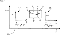
Die
Seitlich am Bondkopf
Die
Die erste Kamera
Die zweite Kamera
Der erste lineare Antrieb des Pick und Place Systems liefert eine Zahl xM und der zweite lineare Antrieb des Pick und Place Systems liefert eine Zahl yM, die zusammen Positionsdaten bilden, die die Position (xM, YM) der Markierung
Der Chipgreifer
Die
Es wird dann noch die Umkehrfunktion F–1 der Abbildungsfunktion F berechnet, so dass
Zudem wird ein erster Korrekturvektor K1 auf den Wert K1 = 0 gesetzt.In addition, a first correction vector K 1 is set to the value K 1 = 0.
Analog wird eine zweite Abbildungsfunktion G, die das zweite Koordinatensystem KS2 auf das dritte Koordinatensystem KS3 abbildet, und ihre Umkehrfunktion G–1 bestimmt. Es gilt dann
Zudem wird ein zweiter Korrekturvektor K2 auf den Wert K2 = 0 gesetzt.In addition, a second correction vector K 2 is set to the value K 2 = 0.
Die erste Kamera
Sobald die Abbildungsfunktionen F und G, ihre Umkehrfunktionen F–1 und G–1, und die Vektoren D1, E1, D2 und E2 ermittelt sind, kann in der Produktionsphase ein Halbleiterchip
- – mit der ersten Kamera
6 ein Bild des als nächster zu montierenden Halbleiterchips2 aufgenommen und aus dem Bild die auf das erste Koordinatensystem KS1 bezogenen Positionsdaten (pW, qW, φW) des Halbleiterchips2 berechnet werden, wobei φw = 0,wenn der Halbleiterchip 2 gegenüber seiner Soll-Lage nicht verdreht ist, - – die auf das dritte Koordinatensystem KS3 bezogene Position (xW, yW), die die Markierung
10 einnehmen muss, damit dieGreifachse 13 des Chipgreifers9 denReferenzpunkt des Halbleiterchips 2 durchstösst, berechnet wird zu(xW, yW) = F[(pW, qW) – D1 – E1 + K1] - – die berechnete Position (xW, yW) angefahren und der Halbleiterchip
2 vom Chipgreifer9 aufgenommen wird, - – mit der zweiten Kamera
7 ein Bild des Substratplatzes aufgenommen wird, auf dem der Halbleiterchip2 zu montieren ist, und aus dem Bild die auf das zweite Koordinatensystem KS2 bezogenen Positionsdaten (uS, vS, ψS) des Substratplatzes berechnet werden, wobei ψS = 0, wenn der Substratplatz gegenüber seiner Soll-Lage nicht verdreht ist, - – die auf das dritte Koordinatensystem KS3 bezogene Position (xS, yS), die die Markierung
10 einnehmen muss, damit dieGreifachse 13 des Chipgreifers9 den Referenzpunkt des Substratplatzes durchstösst, berechnet wird zu(xS, yS) = G[(uS, vS) – D2 – E2 + K2] - – die berechnete Position (xS, yS) angefahren, fakultativ der Chipgreifer
9 um den Winkel ψS – ψS gedreht, und der Halbleiterchip2 auf dem Substratplatz platziert wird.
- - with the
first camera 6 an image of the next to be mountedsemiconductor chip 2 taken and from the image to the first coordinate system KS 1 related position data (p W , q W , φ W ) of thesemiconductor chip 2 where φ w = 0 when thesemiconductor chip 2 is not twisted in relation to its desired position, - - The reference to the third coordinate system KS 3 position (x W , y W ), the
mark 10 must take, so the grippingaxis 13 of the chip gripper9 the reference point of thesemiconductor chip 2 pierces, is calculated to(x W , y W ) = F [(p W , q W ) -D 1 -E 1 + K 1 ] - - The calculated position (x W , y W ) approached and the
semiconductor chip 2 from the chip gripper9 recorded, - - with the
second camera 7 an image of the substrate space is taken, on which thesemiconductor chip 2 is to be mounted, and from the image on the second coordinate system KS 2 related position data (u S , v S , ψ S ) of the substrate space are calculated, where ψ S = 0, when the substrate space is not rotated relative to its desired position, - - The reference to the third coordinate system KS 3 position (x S , y S ), the
mark 10 must take, so the grippingaxis 13 of the chip gripper9 the reference point of the substrate space pierces, is calculated to(x S , y S ) = G [(u S , v S ) - D 2 - E 2 + K 2 ] - - The calculated position (x S , y S ) approached, optionally the chip gripper
9 rotated by the angle ψ S - ψ S , and thesemiconductor chip 2 placed on the substrate place.
Um die hohe Platzierungsgenauigkeit des Die Bonders während der ganzen Produktion auf dem gleich bleibend hohen Niveau zu halten, wird beim Auftreten eines vorbestimmten Ereignisses eine Nachjustierung des ersten Korrekturvektors K1 und des zweiten Korrekturvektors K2 durchgeführt. Dabei wird die am Bondkopf
- – Bewegen des Bondkopfs
8 an eine Soll-Position R = (xR, yR), in der sich die Markierung10 im Blickfeld der ersten Kamera6 befindet, wobei sich die Koordinaten (xR, yR) auf das dritte Koordinatensystem KS3 beziehen, - – Berechnen der Soll-Position (pR, qR) der Markierung
10 in Bezug auf das erste KoordinatensystemKS1 zu (pR, qR) = F–1(xR, yR), - – Aufnehmen eines Bildes der Markierung
10 mit der ersten Kamera6 , aus dem Bild der ersten Kamera6 Ermitteln der Ist-Position (pM, qM) der Markierung10 in Bezug auf das erste Koordinatensystem KS1, und - – Berechnen des ersten Korrekturvektors K1 als Differenz zwischen der angefahrenen Soll-Position und der gemessenen Ist-Position:
K1 = (pR, qR) – (pM, qM).
- - moving the bondhead
8th to a desired position R = (x R , y R ), in which themark 10 in the field of vision of thefirst camera 6 where the coordinates (x R , y R ) refer to the third coordinate system KS 3 , - Calculating the desired position (p R , q R ) of the
mark 10 in relation to the first coordinate systemK S1 to (p R , q R ) = F -1 (x R , y R ), - - Take a picture of the
mark 10 with thefirst camera 6 , from the picture of thefirst camera 6 Determine the actual position (p M , q M ) of the marking10 with respect to the first coordinate system KS 1 , and - Calculating the first correction vector K 1 as the difference between the approached desired position and the measured actual position:
K 1 = (p R , q R ) - (p M , q M ).
Es ist klar, dass sich der erste Korrekturvektor K1 auf das erste Koordinatensystem KS1 bezieht. It is clear that the first correction vector K 1 on the first coordinate system KS 1 refers.
Die Nachjustierung des zweiten Korrekturvektors K2 erfolgt analog durch
- – Bewegen des Bondkopfs
8 an eine Soll-Position T = (xT, yT), in der sich die Markierung10 im Blickfeld der zweiten Kamera7 befindet, wobei sich die Koordinaten (xT, yT) auf das dritte Koordinatensystem KS3 beziehen, - – Berechnen der Soll-Position (uT, vT) der Markierung
10 in Bezug auf das zweite KoordinatensystemKS2 zu (uT, vT) = G–1(xT, yT), - – Aufnehmen eines Bildes der Markierung
10 mit der zweiten Kamera7 , aus dem Bild der zweiten Kamera7 Ermitteln der Ist-Position (uM, vM) der Markierung10 in Bezug auf das zweite Koordinatensystem KS2, und - – Berechnen des zweiten Korrekturvektors K2 als Differenz zwischen der angefahrenen Soll-Position und der gemessenen Ist-Position:
K2 = (uT, vT) – (uM, vM),
- - moving the bondhead
8th to a desired position T = (x T , y T ), in which themark 10 in the field of vision of thesecond camera 7 where the coordinates (x T , y T ) refer to the third coordinate system KS 3 , - - Calculating the target position (u T , v T ) of the
marker 10 with respect to the second coordinate systemKS 2 to (u T , v T ) = G -1 (x T , y T ), - - Take a picture of the
mark 10 with thesecond camera 7 , from the picture of thesecond camera 7 Determine the actual position (u M , v M ) of the marking10 with respect to the second coordinate system KS 2 , and - Calculating the second correction vector K 2 as the difference between the approached desired position and the measured actual position:
K 2 = (u T , v T ) - (u M , v M ),
Es ist klar, dass sich der zweite Korrekturvektor K2 auf das zweite Koordinatensystem KS2 bezieht.It is clear that the second correction vector K 2 refers to the second coordinate system KS 2 .
Es sind verschiedene Ereignisse, die eine Nachjustierung der Korrekturvektoren K1 und K2 auslösen können, insbesondere die folgenden vier Ereignisse:
- – seit der letzten Kalibration ist eine vorbestimmte
Anzahl von Halbleiterchips 2 montiert worden, - – seit der letzten Kalibration hat sich eine an einer vorbestimmten Stelle des Pick
und Place Systems 5 gemessene Temperatur um mehr als einen vorbestimmten Wert verändert, - – die Produktion wurde gestoppt,
- – die Ist-Lage des montierten Halbleiterchips, die mit der zweiten Kamera
7 nach dem Montieren erfasst und berechnet wurde, weicht von der Soll-Lage um mehr als ein vorbestimmtes Mass ab.
- Since the last calibration is a predetermined number of
semiconductor chips 2 been mounted, - - Since the last calibration has one at a predetermined point of the pick and
place system 5 measured temperature changed by more than a predetermined value, - - the production was stopped
- - The actual position of the mounted semiconductor chip, with the
second camera 7 has been detected and calculated after mounting deviates from the target position by more than a predetermined amount.
Nach Abschluss der Nachjustierung der Korrekturvektoren K1 und K2 kann die Montage der Halbleiterchips
Die Erfindung lässt sich bei den bekannten Pick and Place Systemen, bei denen der Wafertisch
Das oben beschriebene Ausführungsbeispiel ist ein bevorzugtes Ausführungsbeispiel, bei dem der Bondkopf für die Justierung und die Nachjustierung an die erste Soll-Position R bzw. die zweite Soll-Position T bewegt wird und die auf das dritte Koordinatensystem KS3 bezogenen Koordinaten der ersten Soll-Position R und der zweiten Soll-Position T gespeichert und für die Nachjustierung der beiden Korrekturvektoren K1 und K2 benützt werden. Bei diesem Beispiel wird die entsprechende Soll-Position der Markierung
Das Pick und Place System umfasst als Teil ein Pick-System für die Entnahme der Halbleiterchips vom Wafertisch. Das dritte Koordinatensystem KS3 ist ein dem Pick-System bzw. dem Pick und Place System immanentes Koordinatensystem und wird deshalb im folgenden als Koordinatensystem KS bezeichnet. Damit die Nachjustierung durchgeführt werden kann, wird zunächst in einer Einrichtungsphase eine Justierung durchgeführt, bei der der Bondkopf
In analoger Weise werden bevorzugt auch Verschiebungen des zweiten Koordinatensystems KS2 der zweiten Kamera
Die Ermittlung der auf das erste Koordinatensystem KS1 bzw. zweite Koordinatensystem KS2 bezogenen Koordinaten des Referenzpunktes umfasst das Aufnehmen eines Bildes mit der entsprechenden Kamera
Die Montage der Halbleiterchips erfolgt dann vorzugsweise indem
- – die mit der ersten Kamera
6 erfasste Position des als nächster zu montierenden Halbleiterchips2 in Form von auf das erste Koordinatensystem KS1 bezogenen Positionsdaten zur Verfügung gestellt wird, - – die mit der zweiten Kamera
7 erfasste Position des Substratplatzes, auf dem der Halbleiterchip2 zu montieren ist, in Form von auf das zweite Koordinatensystem KS1 bezogenen Positionsdaten zur Verfügung gestellt wird, - – in der Einrichtungsphase eine erste Abbildungsfunktion, die das erste Koordinatensystem KS1 auf das Koordinatensystem KS abbildet, und ihre Umkehrfunktion bestimmt wird, ein erster Korrekturvektor auf den Wert Null gesetzt wird, eine zweite Abbildungsfunktion, die das zweite Koordinatensystem KS1 auf das Koordinatensystem KS abbildet, und ihre Umkehrfunktion bestimmt wird und ein zweiter Korrekturvektor auf den Wert Null gesetzt wird, in der
Produktionsphase ein Halbleiterchip 2 nach dem andern montiert wird, indem - – mit der ersten Kamera
6 ein Bild des als nächster zu montierenden Halbleiterchips2 aufgenommen und die Position desHalbleiterchips 2 in Bezug auf das erste Koordinatensystem KS1 ermittelt und daraus mittels der ersten Abbildungsfunktion unter Berücksichtigung des ersten Korrekturvektors die auf das Koordinatensystem KS bezogene Position berechnet wird, an die das Pick undPlace System 5 den Bondkopf 8 bewegen muss, umden Halbleiterchip 2 aufzunehmen, - – mit der zweiten Kamera
7 ein Bild des Substratplatzes aufgenommen wird, auf dem der Halbleiterchip2 zu montieren ist, und die Position des Substratplatzes in Bezug auf das zweite Koordinatensystem KS2 ermittelt und daraus mittels der zweiten Abbildungsfunktion unter Berücksichtigung des zweiten Korrekturvektors die auf das Koordinatensystem KS bezogene Position berechnet wird, an die das Pick undPlace System 5 den Bondkopf 8 bewegen muss, umden Halbleiterchip 2 auf dem Substratplatz zu montieren, und dass die Nachjustierung in der Produktionsphase eine Nachjustierung des ersten Korrekturvektors und des zweiten Korrekturvektors mit folgenden Schritten umfasst: - – Bewegen des Bondkopfs
8 an die erste Soll-Position, - – Aufnehmen eines Bildes der Markierung
10 mit der ersten Kamera6 , aus dem Bild der ersten Kamera6 Ermitteln der Ist-Position der Markierung 10 in Bezug auf das erste Koordinatensystem KS1, und - – Berechnen des ersten Korrekturvektors K1 als Differenz zwischen der gespeicherten Soll-Position und der ermittelten Ist-Position,
- – Bewegen des Bondkopfs
8 an die zweite Soll-Position, - – Aufnehmen eines Bildes der Markierung
10 mit der zweiten Kamera7 , aus dem Bild der zweiten Kamera7 Ermitteln der Ist-Position der Markierung 10 in Bezug auf das zweite Koordinatensystem KS2, und - – Berechnen des zweiten Korrekturvektors K2 als Differenz zwischen der gespeicherten Soll-Position und der ermittelten Ist-Position.
- - the one with the
first camera 6 detected position of the next to be mountedsemiconductor chip 2 is provided in the form of related to the first coordinate system KS 1 position data, - - those with the
second camera 7 detected position of the substrate space on which thesemiconductor chip 2 is to be mounted, is provided in the form of related to the second coordinate system KS 1 position data, - In the setup phase, a first mapping function which maps the first coordinate system KS 1 to the coordinate system KS and determines its inverse function, a first correction vector is set to zero, a second mapping function, the second coordinate system KS 1 to the coordinate system KS and its inverse function is determined and a second correction vector is set to zero, in the production phase a
semiconductor chip 2 after the other is mounted by - - with the
first camera 6 an image of the next to be mountedsemiconductor chip 2 recorded and the position of thesemiconductor chip 2 is determined with respect to the first coordinate system KS 1 and from this the position calculated on the coordinate system KS is calculated by means of the first mapping function, taking into account the first correction vector, to which the pick andplace system 5 the bondhead8th must move to thesemiconductor chip 2 take, - - with the
second camera 7 an image of the substrate space is taken, on which thesemiconductor chip 2 is to be mounted, and determines the position of the substrate space with respect to the second coordinate system KS 2 and from there by means of the second mapping function taking into account the second correction vector, the position on the coordinate system KS is calculated, to which the pick andplace system 5 the bondhead8th must move to thesemiconductor chip 2 to mount on the substrate space, and that the readjustment in the production phase, a readjustment of the first correction vector and the second correction vector comprising the following steps: - - moving the bondhead
8th to the first target position, - - Take a picture of the
mark 10 with thefirst camera 6 , from the picture of thefirst camera 6 Determine the actual position of themarker 10 with respect to the first coordinate system KS 1 , and - Calculating the first correction vector K 1 as the difference between the stored desired position and the determined actual position,
- - moving the bondhead
8th to the second desired position, - - Take a picture of the
mark 10 with thesecond camera 7 , from the picture of thesecond camera 7 Determine the actual position of themarker 10 with respect to the second coordinate system KS 2 , and - - Calculating the second correction vector K 2 as the difference between the stored desired position and the determined actual position.
Claims (4)
Applications Claiming Priority (5)
| Application Number | Priority Date | Filing Date | Title |
|---|---|---|---|
| CH15622007 | 2007-10-09 | ||
| CH1562/07 | 2007-10-09 | ||
| CH1136/08 | 2008-07-17 | ||
| CH11362008A CH698334B1 (en) | 2007-10-09 | 2008-07-17 | A process for the removal and installation of a wafer table provided on the semiconductor chip on a substrate. |
| PCT/EP2008/063268 WO2009047214A2 (en) | 2007-10-09 | 2008-10-03 | Method for picking up semiconductor chips from a wafer table and mounting the removed semiconductor chips on a substrate |
Publications (2)
| Publication Number | Publication Date |
|---|---|
| DE112008002467T5 DE112008002467T5 (en) | 2010-08-26 |
| DE112008002467B4 true DE112008002467B4 (en) | 2013-08-22 |
Family
ID=40908817
Family Applications (1)
| Application Number | Title | Priority Date | Filing Date |
|---|---|---|---|
| DE112008002467T Active DE112008002467B4 (en) | 2007-10-09 | 2008-10-03 | Method for the removal of semiconductor chips from a wafer table and the mounting of the semiconductor chips on a substrate |
Country Status (8)
| Country | Link |
|---|---|
| JP (1) | JP5258068B2 (en) |
| KR (1) | KR101503556B1 (en) |
| CN (1) | CN101861637B (en) |
| CH (1) | CH698334B1 (en) |
| DE (1) | DE112008002467B4 (en) |
| HK (1) | HK1144235A1 (en) |
| MY (1) | MY155097A (en) |
| TW (1) | TWI464820B (en) |
Families Citing this family (21)
| Publication number | Priority date | Publication date | Assignee | Title |
|---|---|---|---|---|
| CN103367208B (en) * | 2013-07-02 | 2015-10-28 | 华中科技大学 | A kind of back bonding platform for superchip |
| KR20170030548A (en) * | 2014-06-11 | 2017-03-17 | 유니버셜 인스트루먼츠 코퍼레이션 | Test device for establishing, verifying, and/or managing accuracy |
| CN104362120B (en) * | 2014-10-30 | 2017-04-19 | 深圳市大能智造科技有限公司 | Camera position adjustment method of visual positioning system of crystal plate pickup device |
| US10223589B2 (en) | 2015-03-03 | 2019-03-05 | Cognex Corporation | Vision system for training an assembly system through virtual assembly of objects |
| JP6510838B2 (en) * | 2015-03-11 | 2019-05-08 | ファスフォードテクノロジ株式会社 | Bonding apparatus and bonding method |
| JP6438826B2 (en) * | 2015-04-02 | 2018-12-19 | ファスフォードテクノロジ株式会社 | Bonding apparatus and bonding method |
| JP6470088B2 (en) * | 2015-04-02 | 2019-02-13 | ファスフォードテクノロジ株式会社 | Bonding apparatus and bonding method |
| DE102015106224B4 (en) * | 2015-04-22 | 2022-09-01 | Asm Assembly Systems Gmbh & Co. Kg | Process for repeated measurement of a component carrier located in a placement area of a placement machine, as well as placement machine and computer program for carrying out this method |
| US10290118B2 (en) | 2015-08-06 | 2019-05-14 | Cognex Corporation | System and method for tying together machine vision coordinate spaces in a guided assembly environment |
| CH711536B1 (en) * | 2015-08-31 | 2019-02-15 | Besi Switzerland Ag | Method for mounting bumped semiconductor chips on substrate sites of a substrate. |
| JP6584234B2 (en) * | 2015-08-31 | 2019-10-02 | ファスフォードテクノロジ株式会社 | Die bonder, bonding method and semiconductor device manufacturing method |
| JP6692376B2 (en) * | 2016-02-01 | 2020-05-13 | 芝浦メカトロニクス株式会社 | Electronic component mounting apparatus and mounting method, and package component manufacturing method |
| CN106409746A (en) * | 2016-10-21 | 2017-02-15 | 合肥矽迈微电子科技有限公司 | Chip upright patching equipment |
| CN108575053B (en) * | 2017-03-08 | 2020-03-27 | 台达电子电源(东莞)有限公司 | Electronic component inserting and positioning device and automatic component inserting machine |
| CN106829469A (en) * | 2017-03-30 | 2017-06-13 | 武汉库柏特科技有限公司 | A kind of unordered grabbing device of robot based on double camera and method |
| JP6649316B2 (en) * | 2017-03-31 | 2020-02-19 | 平田機工株式会社 | Transfer method and transfer system |
| US10923370B2 (en) * | 2017-05-11 | 2021-02-16 | Murata Machinery, Ltd. | Transport system and transport method |
| TWI651795B (en) * | 2017-06-20 | 2019-02-21 | 梭特科技股份有限公司 | Image assist method for placing chip and chip apparatus using the method |
| JP7018341B2 (en) * | 2018-03-26 | 2022-02-10 | ファスフォードテクノロジ株式会社 | Manufacturing method of die bonding equipment and semiconductor equipment |
| CN110767577A (en) * | 2019-10-24 | 2020-02-07 | 苏师大半导体材料与设备研究院(邳州)有限公司 | Semiconductor material attaching method |
| CN112308919B (en) * | 2020-10-28 | 2024-04-09 | 北京半导体专用设备研究所(中国电子科技集团公司第四十五研究所) | Correction method and device for clamping position of chip in clamp |
Citations (3)
| Publication number | Priority date | Publication date | Assignee | Title |
|---|---|---|---|---|
| EP1065917A2 (en) * | 1999-06-29 | 2001-01-03 | Sony Corporation | Calibrating method for part mounting apparatus |
| EP1581040A2 (en) * | 2004-03-26 | 2005-09-28 | Matsushita Electric Industrial Co., Ltd. | Electronic component mounting apparatus and electronic component mounting method |
| WO2008083701A1 (en) * | 2006-12-22 | 2008-07-17 | Kulicke & Soffa Die Bonding Gmbh | Method for calibrating the x-y positioning of a positioning tool, and apparatus with such a positioning tool |
Family Cites Families (11)
| Publication number | Priority date | Publication date | Assignee | Title |
|---|---|---|---|---|
| EP0923111B1 (en) | 1997-12-07 | 2007-05-02 | Oerlikon Assembly Equipment AG, Steinhausen | Semiconductor mounting apparatus with a reciprocating chip gripper |
| JP4046030B2 (en) * | 2002-08-30 | 2008-02-13 | 株式会社村田製作所 | Component mounting method and component mounting apparatus |
| DE10300518B4 (en) * | 2003-01-09 | 2005-06-23 | Siemens Ag | Device for loading substrates with components and method for calibrating such a device |
| ATE333780T1 (en) | 2003-05-21 | 2006-08-15 | Unaxis Int Trading Ltd | SEMICONDUCTOR ASSEMBLY DEVICE |
| CH696103A5 (en) | 2003-06-06 | 2006-12-15 | Esec Trading Sa | Semiconductor assembly equipment. |
| JP4343710B2 (en) * | 2004-01-09 | 2009-10-14 | ヤマハ発動機株式会社 | Surface mount machine |
| JP4029855B2 (en) * | 2004-03-26 | 2008-01-09 | 松下電器産業株式会社 | Electronic component mounting apparatus and electronic component mounting method |
| EP1612843A1 (en) | 2004-07-02 | 2006-01-04 | Unaxis International Trading Ltd | Method and apparatus for mounting semiconductors |
| DE102004036990A1 (en) * | 2004-07-30 | 2006-03-23 | Siemens Ag | Calibration method for assembling machine, involves recording component and marker by camera, and determining actual position of component relative to marker by camera |
| EP1841570A1 (en) * | 2005-01-26 | 2007-10-10 | Abb Ab | Device and method for calibrating the center point of tool mounted on a robot by means of a camera |
| JP2007173801A (en) | 2005-12-22 | 2007-07-05 | Unaxis Internatl Trading Ltd | Method of fitting flip chip to substrate |
-
2008
- 2008-07-17 CH CH11362008A patent/CH698334B1/en not_active IP Right Cessation
- 2008-10-03 KR KR1020107007665A patent/KR101503556B1/en active IP Right Grant
- 2008-10-03 CN CN2008801103578A patent/CN101861637B/en active Active
- 2008-10-03 MY MYPI2010001142A patent/MY155097A/en unknown
- 2008-10-03 JP JP2010528368A patent/JP5258068B2/en active Active
- 2008-10-03 DE DE112008002467T patent/DE112008002467B4/en active Active
- 2008-10-07 TW TW097138530A patent/TWI464820B/en active
-
2010
- 2010-11-19 HK HK10110796.3A patent/HK1144235A1/en unknown
Patent Citations (3)
| Publication number | Priority date | Publication date | Assignee | Title |
|---|---|---|---|---|
| EP1065917A2 (en) * | 1999-06-29 | 2001-01-03 | Sony Corporation | Calibrating method for part mounting apparatus |
| EP1581040A2 (en) * | 2004-03-26 | 2005-09-28 | Matsushita Electric Industrial Co., Ltd. | Electronic component mounting apparatus and electronic component mounting method |
| WO2008083701A1 (en) * | 2006-12-22 | 2008-07-17 | Kulicke & Soffa Die Bonding Gmbh | Method for calibrating the x-y positioning of a positioning tool, and apparatus with such a positioning tool |
Also Published As
| Publication number | Publication date |
|---|---|
| HK1144235A1 (en) | 2011-02-02 |
| KR101503556B1 (en) | 2015-03-17 |
| MY155097A (en) | 2015-09-15 |
| JP5258068B2 (en) | 2013-08-07 |
| CN101861637A (en) | 2010-10-13 |
| CH698334B1 (en) | 2011-07-29 |
| CH698334A1 (en) | 2009-07-15 |
| DE112008002467T5 (en) | 2010-08-26 |
| JP2010541293A (en) | 2010-12-24 |
| CN101861637B (en) | 2012-07-18 |
| KR20100085027A (en) | 2010-07-28 |
| TWI464820B (en) | 2014-12-11 |
| TW200929425A (en) | 2009-07-01 |
Similar Documents
| Publication | Publication Date | Title |
|---|---|---|
| DE112008002467B4 (en) | Method for the removal of semiconductor chips from a wafer table and the mounting of the semiconductor chips on a substrate | |
| DE102018109512B4 (en) | Device and method for mounting components on a substrate | |
| DE102016114337B4 (en) | SYSTEM AND METHOD FOR CONNECTING COORDINATE SPACES MACHINES LIKE ASSEMBLY FIXED IN AN ENVIRONMENT | |
| DE112009000667B4 (en) | Dispensing device and method for dispensing material onto a substrate | |
| EP2227356B1 (en) | Method and system for extremely precise positioning of at least one object in the end position of a space | |
| EP2126645B1 (en) | Method for calibrating the x-y positioning of a positioning tool, and apparatus with such a positioning tool | |
| DE60312573T2 (en) | Method for locating and setting marking points of a semiconductor device on a substrate | |
| DE10133448A1 (en) | Alignment of cutting blade includes determining angle between tracks from workpiece surface image, determining correction angle per track, setting tracks parallel to x-axis | |
| DE102016113328B4 (en) | Method for mounting bumped semiconductor chips on substrate sites of a substrate | |
| DE102004043282B4 (en) | Method for adjusting the bonding head of a die bonder | |
| EP2859580B1 (en) | Apparatus and method for ascertaining orientation errors | |
| EP1716586A1 (en) | Device for inspecting and rotating electronic components | |
| DE69724894T2 (en) | ASSEMBLY METHOD OF COMPONENTS ON A SUBSTRATE AND ASSEMBLY MACHINE THEREFOR | |
| WO2002102127A1 (en) | Device for assembling components on a substrate | |
| DE102007058293A1 (en) | Calibrating device for adjusting robot coordinate system of industrial robot, has base carrier and multiple markers which are indirectly fastened to base carrier and lie in level | |
| DE102013207599A1 (en) | Placement device and placement method for accurately aligning and / or equipping a substrate with a component | |
| EP1941536B1 (en) | Method and device for the placement of electronic components, in particular semiconductor chips, on a substrate | |
| EP1802192A1 (en) | Method for mounting a flip chip on a substrate | |
| DE112011100388T5 (en) | Method and apparatus for transferring chips from a wafer | |
| DE10012081A1 (en) | Automatic positioning involves acquiring substrate image before moving gripper into acquisition device field of view, acquiring component image, evaluating position difference | |
| CH711536A1 (en) | <TITLE> Method for the assembly of bumped semiconductor chips on substrate locations of a substrate. | |
| DE102018117825A1 (en) | Fitting a component carrier using offset information between structural features formed on opposite sides of a reference component | |
| EP1432013A1 (en) | Semiconductor-mounting apparatus for dispensing an adhesive on a substrat | |
| EP1925023A1 (en) | Method and device for depositing electronic components on a substrate | |
| DE102017125932A1 (en) | Method for bonding electrical, electronic, optical, opto-electrical and / or mechanical components to substrates and an associated bonding device |
Legal Events
| Date | Code | Title | Description |
|---|---|---|---|
| OP8 | Request for examination as to paragraph 44 patent law | ||
| R079 | Amendment of ipc main class |
Free format text: PREVIOUS MAIN CLASS: H01L0021000000 Ipc: H01L0021580000 Effective date: 20110705 |
|
| R082 | Change of representative |
Representative=s name: WOLF & WOLF PATENT- UND RECHTSANWAELTE, DE Representative=s name: WOLF & WOLF PATENT- UND RECHTSANWAELTE GBR, DE Representative=s name: WOLF & WOLF PATENT- UND RECHTSANWALTSGESELLSCH, DE |
|
| R016 | Response to examination communication | ||
| R079 | Amendment of ipc main class |
Free format text: PREVIOUS MAIN CLASS: H01L0021580000 Ipc: H01L0021670000 |
|
| R018 | Grant decision by examination section/examining division | ||
| R079 | Amendment of ipc main class |
Free format text: PREVIOUS MAIN CLASS: H01L0021580000 Ipc: H01L0021670000 Effective date: 20130415 |
|
| R020 | Patent grant now final |
Effective date: 20131123 |
|
| R081 | Change of applicant/patentee |
Owner name: BESI SWITZERLAND AG, CH Free format text: FORMER OWNER: ESEC AG, CHAM, CH |
|
| R082 | Change of representative |
Representative=s name: IP.DESIGN, CH |