DE102011104159A1 - METHOD FOR THE ELECTRICAL CONNECTION OF SEVERAL SOLAR CELLS AND PHOTOVOLTAIC MODULE - Google Patents
METHOD FOR THE ELECTRICAL CONNECTION OF SEVERAL SOLAR CELLS AND PHOTOVOLTAIC MODULE Download PDFInfo
- Publication number
- DE102011104159A1 DE102011104159A1 DE102011104159A DE102011104159A DE102011104159A1 DE 102011104159 A1 DE102011104159 A1 DE 102011104159A1 DE 102011104159 A DE102011104159 A DE 102011104159A DE 102011104159 A DE102011104159 A DE 102011104159A DE 102011104159 A1 DE102011104159 A1 DE 102011104159A1
- Authority
- DE
- Germany
- Prior art keywords
- metal layer
- solar cell
- carrier substrate
- substrate
- metal
- Prior art date
- Legal status (The legal status is an assumption and is not a legal conclusion. Google has not performed a legal analysis and makes no representation as to the accuracy of the status listed.)
- Withdrawn
Links
- 238000000034 method Methods 0.000 title claims abstract description 55
- 239000000758 substrate Substances 0.000 claims abstract description 187
- 229910052751 metal Inorganic materials 0.000 claims abstract description 182
- 239000002184 metal Substances 0.000 claims abstract description 182
- 230000005855 radiation Effects 0.000 claims abstract description 43
- 230000002427 irreversible effect Effects 0.000 claims abstract description 6
- 230000001678 irradiating effect Effects 0.000 claims abstract description 3
- 239000000463 material Substances 0.000 claims description 25
- 238000010521 absorption reaction Methods 0.000 claims description 12
- 238000010438 heat treatment Methods 0.000 claims description 7
- 150000002739 metals Chemical class 0.000 claims description 6
- 239000011888 foil Substances 0.000 claims 1
- 239000012811 non-conductive material Substances 0.000 claims 1
- 238000005476 soldering Methods 0.000 abstract description 6
- 238000001465 metallisation Methods 0.000 description 38
- XAGFODPZIPBFFR-UHFFFAOYSA-N aluminium Chemical compound [Al] XAGFODPZIPBFFR-UHFFFAOYSA-N 0.000 description 14
- 229910052782 aluminium Inorganic materials 0.000 description 12
- 238000002844 melting Methods 0.000 description 8
- 238000004519 manufacturing process Methods 0.000 description 7
- 230000008018 melting Effects 0.000 description 7
- 239000004065 semiconductor Substances 0.000 description 6
- XUIMIQQOPSSXEZ-UHFFFAOYSA-N Silicon Chemical compound [Si] XUIMIQQOPSSXEZ-UHFFFAOYSA-N 0.000 description 5
- 230000005496 eutectics Effects 0.000 description 5
- 229910052710 silicon Inorganic materials 0.000 description 5
- 239000010703 silicon Substances 0.000 description 5
- 230000006378 damage Effects 0.000 description 4
- 238000005516 engineering process Methods 0.000 description 4
- 235000012431 wafers Nutrition 0.000 description 4
- BQCADISMDOOEFD-UHFFFAOYSA-N Silver Chemical compound [Ag] BQCADISMDOOEFD-UHFFFAOYSA-N 0.000 description 3
- 239000000853 adhesive Substances 0.000 description 3
- 230000001070 adhesive effect Effects 0.000 description 3
- 239000011521 glass Substances 0.000 description 3
- 239000007788 liquid Substances 0.000 description 3
- 239000012071 phase Substances 0.000 description 3
- 229910052709 silver Inorganic materials 0.000 description 3
- 239000004332 silver Substances 0.000 description 3
- 238000005245 sintering Methods 0.000 description 3
- 229910000679 solder Inorganic materials 0.000 description 3
- 238000003466 welding Methods 0.000 description 3
- 239000005038 ethylene vinyl acetate Substances 0.000 description 2
- 239000010408 film Substances 0.000 description 2
- 238000003475 lamination Methods 0.000 description 2
- 239000007791 liquid phase Substances 0.000 description 2
- 238000007639 printing Methods 0.000 description 2
- 230000009467 reduction Effects 0.000 description 2
- 230000035882 stress Effects 0.000 description 2
- 230000008646 thermal stress Effects 0.000 description 2
- 239000000654 additive Substances 0.000 description 1
- 230000000996 additive effect Effects 0.000 description 1
- AZDRQVAHHNSJOQ-UHFFFAOYSA-N alumane Chemical group [AlH3] AZDRQVAHHNSJOQ-UHFFFAOYSA-N 0.000 description 1
- 238000000149 argon plasma sintering Methods 0.000 description 1
- 230000015572 biosynthetic process Effects 0.000 description 1
- DQXBYHZEEUGOBF-UHFFFAOYSA-N but-3-enoic acid;ethene Chemical compound C=C.OC(=O)CC=C DQXBYHZEEUGOBF-UHFFFAOYSA-N 0.000 description 1
- 230000015556 catabolic process Effects 0.000 description 1
- 230000000295 complement effect Effects 0.000 description 1
- 239000002131 composite material Substances 0.000 description 1
- 150000001875 compounds Chemical class 0.000 description 1
- 238000010276 construction Methods 0.000 description 1
- 230000007797 corrosion Effects 0.000 description 1
- 238000005260 corrosion Methods 0.000 description 1
- 230000006735 deficit Effects 0.000 description 1
- 238000006731 degradation reaction Methods 0.000 description 1
- 230000001419 dependent effect Effects 0.000 description 1
- 238000000151 deposition Methods 0.000 description 1
- 238000009792 diffusion process Methods 0.000 description 1
- 230000000694 effects Effects 0.000 description 1
- 238000005538 encapsulation Methods 0.000 description 1
- 239000000945 filler Substances 0.000 description 1
- 229920005570 flexible polymer Polymers 0.000 description 1
- 239000011810 insulating material Substances 0.000 description 1
- 238000012432 intermediate storage Methods 0.000 description 1
- 150000002736 metal compounds Chemical class 0.000 description 1
- 229910001092 metal group alloy Inorganic materials 0.000 description 1
- 239000000203 mixture Substances 0.000 description 1
- 238000002161 passivation Methods 0.000 description 1
- 230000035515 penetration Effects 0.000 description 1
- 229920001200 poly(ethylene-vinyl acetate) Polymers 0.000 description 1
- 229920001296 polysiloxane Polymers 0.000 description 1
- 239000002994 raw material Substances 0.000 description 1
- 238000007650 screen-printing Methods 0.000 description 1
- 230000035945 sensitivity Effects 0.000 description 1
- 238000007711 solidification Methods 0.000 description 1
- 230000008023 solidification Effects 0.000 description 1
- 238000010257 thawing Methods 0.000 description 1
- 239000010409 thin film Substances 0.000 description 1
- 238000007740 vapor deposition Methods 0.000 description 1
Images


Classifications
-
- H—ELECTRICITY
- H01—ELECTRIC ELEMENTS
- H01L—SEMICONDUCTOR DEVICES NOT COVERED BY CLASS H10
- H01L25/00—Assemblies consisting of a plurality of individual semiconductor or other solid state devices ; Multistep manufacturing processes thereof
- H01L25/03—Assemblies consisting of a plurality of individual semiconductor or other solid state devices ; Multistep manufacturing processes thereof all the devices being of a type provided for in the same subgroup of groups H01L27/00 - H01L33/00, or in a single subclass of H10K, H10N, e.g. assemblies of rectifier diodes
- H01L25/04—Assemblies consisting of a plurality of individual semiconductor or other solid state devices ; Multistep manufacturing processes thereof all the devices being of a type provided for in the same subgroup of groups H01L27/00 - H01L33/00, or in a single subclass of H10K, H10N, e.g. assemblies of rectifier diodes the devices not having separate containers
- H01L25/041—Assemblies consisting of a plurality of individual semiconductor or other solid state devices ; Multistep manufacturing processes thereof all the devices being of a type provided for in the same subgroup of groups H01L27/00 - H01L33/00, or in a single subclass of H10K, H10N, e.g. assemblies of rectifier diodes the devices not having separate containers the devices being of a type provided for in group H01L31/00
- H01L25/042—Assemblies consisting of a plurality of individual semiconductor or other solid state devices ; Multistep manufacturing processes thereof all the devices being of a type provided for in the same subgroup of groups H01L27/00 - H01L33/00, or in a single subclass of H10K, H10N, e.g. assemblies of rectifier diodes the devices not having separate containers the devices being of a type provided for in group H01L31/00 the devices being arranged next to each other
-
- H—ELECTRICITY
- H01—ELECTRIC ELEMENTS
- H01L—SEMICONDUCTOR DEVICES NOT COVERED BY CLASS H10
- H01L31/00—Semiconductor devices sensitive to infrared radiation, light, electromagnetic radiation of shorter wavelength or corpuscular radiation and specially adapted either for the conversion of the energy of such radiation into electrical energy or for the control of electrical energy by such radiation; Processes or apparatus specially adapted for the manufacture or treatment thereof or of parts thereof; Details thereof
- H01L31/04—Semiconductor devices sensitive to infrared radiation, light, electromagnetic radiation of shorter wavelength or corpuscular radiation and specially adapted either for the conversion of the energy of such radiation into electrical energy or for the control of electrical energy by such radiation; Processes or apparatus specially adapted for the manufacture or treatment thereof or of parts thereof; Details thereof adapted as photovoltaic [PV] conversion devices
- H01L31/042—PV modules or arrays of single PV cells
- H01L31/05—Electrical interconnection means between PV cells inside the PV module, e.g. series connection of PV cells
- H01L31/0504—Electrical interconnection means between PV cells inside the PV module, e.g. series connection of PV cells specially adapted for series or parallel connection of solar cells in a module
- H01L31/0516—Electrical interconnection means between PV cells inside the PV module, e.g. series connection of PV cells specially adapted for series or parallel connection of solar cells in a module specially adapted for interconnection of back-contact solar cells
-
- H—ELECTRICITY
- H01—ELECTRIC ELEMENTS
- H01L—SEMICONDUCTOR DEVICES NOT COVERED BY CLASS H10
- H01L31/00—Semiconductor devices sensitive to infrared radiation, light, electromagnetic radiation of shorter wavelength or corpuscular radiation and specially adapted either for the conversion of the energy of such radiation into electrical energy or for the control of electrical energy by such radiation; Processes or apparatus specially adapted for the manufacture or treatment thereof or of parts thereof; Details thereof
- H01L31/04—Semiconductor devices sensitive to infrared radiation, light, electromagnetic radiation of shorter wavelength or corpuscular radiation and specially adapted either for the conversion of the energy of such radiation into electrical energy or for the control of electrical energy by such radiation; Processes or apparatus specially adapted for the manufacture or treatment thereof or of parts thereof; Details thereof adapted as photovoltaic [PV] conversion devices
- H01L31/042—PV modules or arrays of single PV cells
- H01L31/0445—PV modules or arrays of single PV cells including thin film solar cells, e.g. single thin film a-Si, CIS or CdTe solar cells
-
- H—ELECTRICITY
- H01—ELECTRIC ELEMENTS
- H01L—SEMICONDUCTOR DEVICES NOT COVERED BY CLASS H10
- H01L31/00—Semiconductor devices sensitive to infrared radiation, light, electromagnetic radiation of shorter wavelength or corpuscular radiation and specially adapted either for the conversion of the energy of such radiation into electrical energy or for the control of electrical energy by such radiation; Processes or apparatus specially adapted for the manufacture or treatment thereof or of parts thereof; Details thereof
- H01L31/04—Semiconductor devices sensitive to infrared radiation, light, electromagnetic radiation of shorter wavelength or corpuscular radiation and specially adapted either for the conversion of the energy of such radiation into electrical energy or for the control of electrical energy by such radiation; Processes or apparatus specially adapted for the manufacture or treatment thereof or of parts thereof; Details thereof adapted as photovoltaic [PV] conversion devices
- H01L31/042—PV modules or arrays of single PV cells
- H01L31/05—Electrical interconnection means between PV cells inside the PV module, e.g. series connection of PV cells
- H01L31/0504—Electrical interconnection means between PV cells inside the PV module, e.g. series connection of PV cells specially adapted for series or parallel connection of solar cells in a module
-
- H—ELECTRICITY
- H01—ELECTRIC ELEMENTS
- H01L—SEMICONDUCTOR DEVICES NOT COVERED BY CLASS H10
- H01L31/00—Semiconductor devices sensitive to infrared radiation, light, electromagnetic radiation of shorter wavelength or corpuscular radiation and specially adapted either for the conversion of the energy of such radiation into electrical energy or for the control of electrical energy by such radiation; Processes or apparatus specially adapted for the manufacture or treatment thereof or of parts thereof; Details thereof
- H01L31/18—Processes or apparatus specially adapted for the manufacture or treatment of these devices or of parts thereof
- H01L31/1876—Particular processes or apparatus for batch treatment of the devices
- H01L31/188—Apparatus specially adapted for automatic interconnection of solar cells in a module
-
- H—ELECTRICITY
- H01—ELECTRIC ELEMENTS
- H01L—SEMICONDUCTOR DEVICES NOT COVERED BY CLASS H10
- H01L2924/00—Indexing scheme for arrangements or methods for connecting or disconnecting semiconductor or solid-state bodies as covered by H01L24/00
- H01L2924/0001—Technical content checked by a classifier
- H01L2924/0002—Not covered by any one of groups H01L24/00, H01L24/00 and H01L2224/00
-
- Y—GENERAL TAGGING OF NEW TECHNOLOGICAL DEVELOPMENTS; GENERAL TAGGING OF CROSS-SECTIONAL TECHNOLOGIES SPANNING OVER SEVERAL SECTIONS OF THE IPC; TECHNICAL SUBJECTS COVERED BY FORMER USPC CROSS-REFERENCE ART COLLECTIONS [XRACs] AND DIGESTS
- Y02—TECHNOLOGIES OR APPLICATIONS FOR MITIGATION OR ADAPTATION AGAINST CLIMATE CHANGE
- Y02E—REDUCTION OF GREENHOUSE GAS [GHG] EMISSIONS, RELATED TO ENERGY GENERATION, TRANSMISSION OR DISTRIBUTION
- Y02E10/00—Energy generation through renewable energy sources
- Y02E10/50—Photovoltaic [PV] energy
Landscapes
- Engineering & Computer Science (AREA)
- Power Engineering (AREA)
- Microelectronics & Electronic Packaging (AREA)
- Physics & Mathematics (AREA)
- Condensed Matter Physics & Semiconductors (AREA)
- General Physics & Mathematics (AREA)
- Computer Hardware Design (AREA)
- Sustainable Development (AREA)
- Life Sciences & Earth Sciences (AREA)
- Electromagnetism (AREA)
- Sustainable Energy (AREA)
- Manufacturing & Machinery (AREA)
- Photovoltaic Devices (AREA)
Abstract
Es wird ein Verfahren zum Metallisieren und Verbinden von Solarzellensubstraten (1) sowie ein Photovoltaikmodul (100) aus mehreren metallisierten und miteinander elektrisch verbundenen Solarzellen (20) beschrieben. Ein Solarzellensubstrat (1), in dem optional elektrische Metallkontakte bildende zweite Metallschichten (2a, 2b) vorgesehen sind, wird an ein Trägersubstrat (4) angelagert, an dessen Oberfläche wenigstens eine erste Metallschicht (3) in einem geeigneten Muster ausgebildet ist. Durch lokales Bestrahlen der Metallschicht (2, 3) mit Laserstrahlung (5, 6) durch das Solarzellensubstrat (1) oder das Trägersubstrat (4) hindurch wird Energie derart eingebracht, dass die Metallschicht (2, 3) durch absorbierte Laserstrahlung (5, 6) für ein irreversibles Verbinden mit der angrenzenden Oberfläche des Solarzellensubstrates (1) erhitzt wird. Durch das Laserbonden der an dem Trägersubstrat (4) vorgesehenen Metallschicht (3) an das Solarzellensubstrat (1) können Solarzellen zu einem Photovoltaikmodul verschaltet werden, wobei auf die herkömmliche Verlötung benachbarter Solarzellen über Metallbändchen verzichtet werden kann. Es können somit nicht-lötbare, kostengünstige, insbesondere Silber-freie Metallschichten (2a, 2b) für die Kontaktierung der Solarzellensubstrate (1) der Solarzellen (20) verwendet werden.A method for metallizing and connecting solar cell substrates (1) and a photovoltaic module (100) made up of several metallized and electrically connected solar cells (20) are described. A solar cell substrate (1), in which second metal layers (2a, 2b) optionally forming electrical metal contacts are provided, is attached to a carrier substrate (4), on the surface of which at least one first metal layer (3) is formed in a suitable pattern. By locally irradiating the metal layer (2, 3) with laser radiation (5, 6) through the solar cell substrate (1) or the carrier substrate (4), energy is introduced in such a way that the metal layer (2, 3) is absorbed by laser radiation (5, 6 ) is heated for an irreversible connection with the adjacent surface of the solar cell substrate (1). By laser bonding the metal layer (3) provided on the carrier substrate (4) to the solar cell substrate (1), solar cells can be interconnected to form a photovoltaic module, whereby the conventional soldering of neighboring solar cells via metal strips can be dispensed with. Thus, non-solderable, inexpensive, in particular silver-free metal layers (2a, 2b) can be used for contacting the solar cell substrates (1) of the solar cells (20).
Description
GEBIET DER ERFINDUNGFIELD OF THE INVENTION
Die vorliegende Erfindung betrifft ein Verfahren zum Metallisieren und elektrischen Verbinden mehrerer Solarzellen. Die Erfindung betrifft ferner ein entsprechend ausgebildetes Photovoltaikmodul.The present invention relates to a method for metallizing and electrically connecting a plurality of solar cells. The invention further relates to a suitably designed photovoltaic module.
TECHNISCHER HINTERGRUNDTECHNICAL BACKGROUND
Substrate für Solarzellen müssen häufig an ihrer Oberfläche metallisiert werden, beispielsweise, um einen elektrischen Kontakt mit der Solarzelle zu ermöglichen, und insbesondere, um verschiedene Solarzellen elektrisch miteinander verbinden zu können. Dabei soll eine Metallisierung von Solarzellen einerseits mechanisch widerstandsfähig und somit z. B. über eine typische Lebensdauer von Solarzellenmodulen von beispielsweise 30 Jahren stabil sein, um Degradationseffekte so gering wie möglich zu halten. Andererseits soll mit Hilfe der Metallisierung eine gute elektrische Kontaktierung der Solarzellensubstrate bei möglichst geringem elektrischem Widerstand erzielt werden können. Außerdem sollte die Metallisierung im industriellen Maßstab zuverlässig und kostengünstig durchgeführt werden können.Substrates for solar cells often have to be metallized on their surface, for example in order to enable electrical contact with the solar cell, and in particular in order to electrically connect different solar cells with each other. This is a metallization of solar cells on the one hand mechanically resistant and thus z. B. be stable over a typical life of solar cell modules, for example, 30 years, to minimize degradation effects as possible. On the other hand, a good electrical contacting of the solar cell substrates with the lowest possible electrical resistance should be achieved with the aid of metallization. In addition, industrial scale metallization should be reliable and inexpensive.
Zur Herstellung von Photovoltaikmodulen werden mehrere Solarzellen bisher in einem industriellen Standardprozess meist thermisch durch Metallbändchen miteinander verbunden und zu einem Modul verschaltet. Eine elektrische Kontaktierung der Solarzellen untereinander, seriell oder parallel über die Metallbändchen, erfolgt dabei in der Regel durch Infrarotlöten oder konventionelles Löten.For the production of photovoltaic modules, several solar cells are usually connected together in an industrial standard process usually thermally by metal strips and interconnected to form a module. An electrical contacting of the solar cells with each other, serially or in parallel via the metal strips, is usually done by infrared soldering or conventional soldering.
Während des Lötvorgangs können thermische Belastungen im Schichtverbund der Solarzelle oder in der Metallisierung zur Verschaltung mehrerer Solarzellen zu einer Schädigung oder Zerstörung führen. Dies kann insbesondere bei Wafer-basierten Solarzellen kritisch sein, deren Dicke im Zuge von Kostenreduzierungen von aktuell etwa 200 μm auf in Zukunft unter 50 μm bei gleichbleibender Effizienz sinken soll. Bei derart dünnen Solarzellen können aufgrund der Empfindlichkeit der Wafer beim Löten erhöhte Bruchraten auftreten, was die Entwicklung alternativer Metallisierungsverfahren nötig machen kann.During the soldering process, thermal stresses in the composite layer of the solar cell or in the metallization for interconnecting a plurality of solar cells can lead to damage or destruction. This can be particularly critical in wafer-based solar cells whose thickness in the course of cost reductions from currently about 200 microns in the future below 50 microns with the same efficiency should decrease. With such thin solar cells, increased breakage rates can occur due to the sensitivity of the wafers during soldering, which may necessitate the development of alternative metallization processes.
Auch neuartige Zellkonzepte, die beispielsweise beide Kontakttypen an der selben Oberfläche der Solarzelle aufweisen, können neue schädigungsarme und kosteneffiziente Verfahren zur Metallisierung und damit zur elektrischen Kontaktierung und Verschaltung nötig machen.Even novel cell concepts, for example, have both types of contact on the same surface of the solar cell, can make new low-damage and cost-efficient process for metallization and thus for electrical contacting and interconnection necessary.
Hinzu kommt, dass die Verschaltung von Solarzellen unter Verwendung von zu verlötenden Metallbändchen aufgrund eines hohen Arbeitsaufwandes sowie aufgrund von zu verwendender Materialien für die Metallisierung einen erheblichen Kostenbeitrag bei der Fertigung von Photovoltaikmodulen bewirken kann. Um die einzelnen Solarzellen beispielsweise mit den Metallbändchen verlöten zu können, müssen an den Solarzellen lötbare Kontakte vorgesehen sein. Standardmäßig werden hierzu industrielle Solarzellen im Allgemeinen mit Siebdruckpasten auf Basis von Silber metallisiert. Aufgrund stark gestiegener Rohstoffpreise für Silber wird nach alternativen Materialien für die Metallisierung von Solarzellen gesucht. Sofern diese jedoch nicht selbst lötbar sind, war bisher ein aufwändiges und kostenintensives Aufbringen weiterer metallischer, lötfähiger Schichten notwendig.In addition, the interconnection of solar cells using metal strips to be soldered can cause a considerable cost contribution in the production of photovoltaic modules due to a high workload and due to materials to be used for the metallization. In order to solder the individual solar cells, for example, with the metal strip, solderable contacts must be provided on the solar cells. By default, industrial solar cells are generally metallized with screen-printing pastes based on silver. Due to the sharp rise in raw material prices for silver, alternative materials are being sought for the metallization of solar cells. However, if these are not themselves solderable, was previously a costly and costly application of additional metallic, solderable layers necessary.
ZUSAMMENFASSUNG DER ERFINDUNGSUMMARY OF THE INVENTION
Es kann daher ein Bedürfnis an einem Verfahren zum Metallisieren und elektrischen Verbinden von Solarzellen, beispielsweise einem Verfahren zum Verschalten von Solarzellen zu einem Photovoltaikmodul, bestehen, bei denen insbesondere oben genannte Defizite herkömmlicher Metallisierungsverfahren überwunden oder reduziert werden. Insbesondere kann ein Bedürfnis an einem zuverlässigen, kostengünstigen und/oder einfach im industriellen Maßstab zu realisierenden Metallisierungsverfahren für Solarzellen bestehen. Ferner kann ein Bedürfnis an einem Photovoltaikmodul bestehen, das insbesondere aufgrund seiner herstellungsbedingten Struktur eine verbesserte Zuverlässigkeit bei hoher Effizienz und geringen Herstellungskosten ermöglicht.There may therefore be a need for a method for metallizing and electrically connecting solar cells, for example a method for connecting solar cells to a photovoltaic module, in which, in particular, the abovementioned deficits of conventional metallization methods are overcome or reduced. In particular, there may be a need for a reliable, cost-effective and / or simply to be implemented on an industrial scale metallization process for solar cells. Further, there may be a need for a photovoltaic module which, due in particular to its manufacturing structure, enables improved reliability with high efficiency and low manufacturing cost.
Solche Bedürfnisse können mit dem Verfahren und Photovoltaikmodul gemäß den unabhängigen Ansprüchen gedeckt werden. Vorteilhafte Ausführungsformen der Erfindung sind in den abhängigen Ansprüchen definiert.Such needs can be met with the method and photovoltaic module according to the independent claims. Advantageous embodiments of the invention are defined in the dependent claims.
Gemäß einem ersten Aspekt der vorliegenden Erfindung wird ein Verfahren zum Metallisieren und elektrischen Verbinden mehrerer Solarzellen vorgeschlagen. Das Verfahren weist die folgenden Verfahrensschritte auf: Bereitstellen mehrerer Solarzellensubstrate; Bereitstellen eines Trägersubstrates, welches an einer Oberfläche wenigstens eine fest mit dem Trägersubstrat verbundene erste Metallschicht trägt; Anlagern der Solarzellensubstrate jeweils mit einer Oberfläche eines Solarzellensubstrates angrenzend an die erste Metallschicht an dem Trägersubstrat; Einbringen von Energie in die Metallschicht durch lokales Bestrahlen mit Laserstrahlung derart, dass die Laserstrahlung durch wenigstens eines der Solarzellensubstrate und/oder des Trägersubstrates hindurch in einer Richtung bin zu der Metallschicht transmittiert wird, und dass die erste Metallschicht aufgrund von Erhitzung durch absorbierte Laserstrahlung mit dem angrenzenden Solarzellensubstrat irreversibel verbunden wird.According to a first aspect of the present invention, a method for metallizing and electrically connecting a plurality of solar cells is proposed. The method comprises the following method steps: providing a plurality of solar cell substrates; Providing a carrier substrate which carries on a surface at least one first metal layer fixedly connected to the carrier substrate; Depositing the solar cell substrates each having a surface of a solar cell substrate adjacent to the first metal layer on the support substrate; Introducing energy into the metal layer by locally irradiating with laser radiation such that the laser radiation is transmitted through at least one of the solar cell substrates and / or the carrier substrate in a direction toward the metal layer, and that the first metal layer is absorbed by heating Laser radiation is irreversibly connected to the adjacent solar cell substrate.
Dieser Aspekt der Erfindung kann unter anderem als auf der folgenden Idee basierend angesehen werden: Es wurde erkannt, dass Solarzellen dadurch metallisiert und somit elektrisch kontaktiert werden können, dass eine Oberfläche eines Solarzellensubstrates an eine Metallschicht angelegt und mit dieser mechanisch in Kontakt gebracht wird, und die Metallschicht dann mit Hilfe eines Lasers derart bestrahlt wird, dass sie sich lokal stark erhitzt. Die derart erhitzte Metallschicht kann dabei mit der Oberfläche des Solarzellensubstrates zusammenbonden, das heißt, eine mechanisch haftende und elektrisch leitende irreversible Verbindung mit dieser eingehen. Wie weiter unten genauer beschrieben, kann es bei einem solchen Banden oder Verbinden zu einem temporären Verflüssigen von Metall aus der Metallschicht kommen, was einem Laserschweißen entsprechen kann. Alternativ kann die Laserstrahlung für den Bondvorgang derart eingestellt sein, dass es zu einem Zusammensintern der Metallschicht und der Oberfläche des Solarzellensubstrates oder zur Bildung einer flüssigen eutektischen Phase zwischen der Metallschicht und der Oberfläche des Solarzellensubstrates kommt. Die Laserstrahlung kann dabei derart eingestrahlt werden, dass sie durch das Solarzellensubstrat und/oder durch das Trägersubstrat hindurchstrahlt, wobei die Eigenschaften der verwendeten Laserstrahlung derart gewählt sein sollten, dass das Material des jeweiligen Substrates weitgehend transparent für die Laserstrahlung ist und es somit erst an der Metallschicht zu einer wesentlichen Absorption der Laserstrahlung kommt.This aspect of the invention may, inter alia, be considered to be based on the following idea: It has been recognized that solar cells can thereby be metallized and thus electrically contacted, that a surface of a solar cell substrate is applied to and mechanically brought into contact with a metal layer, and the metal layer is then irradiated with the aid of a laser in such a way that it heats up strongly locally. The thus heated metal layer can bond together with the surface of the solar cell substrate, that is, enter into a mechanically adhesive and electrically conductive irreversible connection with this. As will be described in more detail below, such bonding or bonding may result in temporary metallogging of the metal layer, which may correspond to laser welding. Alternatively, the laser radiation for the bonding process can be set in such a way that sintering of the metal layer and the surface of the solar cell substrate or formation of a liquid eutectic phase takes place between the metal layer and the surface of the solar cell substrate. In this case, the laser radiation can be irradiated in such a way that it radiates through the solar cell substrate and / or through the carrier substrate, wherein the properties of the laser radiation used should be selected such that the material of the respective substrate is largely transparent to the laser radiation and thus only at the Metal layer to a substantial absorption of the laser radiation comes.
Das vorgeschlagene Metallisierungsverfahren ermöglicht eine zuverlässige, kostengünstige, schnelle und einfache Metallisierung und elektrische Kontaktierung von Solarzellensubstraten.The proposed metallization process enables reliable, cost-effective, quick and easy metallization and electrical contacting of solar cell substrates.
Nachfolgend werden mögliche Details und Vorteile von Ausführungsformen des vorgeschlagenen Metallisierungs- und Verbindungsverfahrens beschrieben.Hereinafter, possible details and advantages of embodiments of the proposed metallization and bonding method will be described.
Das bereitgestellte Solarzellensubstrat kann aus einem beliebigen Halbleitermaterial bestehen. Das Metallisierungsverfahren ist insbesondere zur Metallisierung von dünnen Siliziumwafern mit einer Dicke von beispielsweise weniger als 200 μm, vorzugsweise weniger als 100 μm geeignet, da hohe mechanische Beanspruchungen des Solarzellensubstrates vermieden werden.The provided solar cell substrate may be made of any semiconductor material. The metallization process is particularly suitable for the metallization of thin silicon wafers having a thickness of, for example, less than 200 .mu.m, preferably less than 100 .mu.m, since high mechanical stresses on the solar cell substrate are avoided.
Die Begriffe „Solarzelle” und „Solarzellensubstrat” werden hierin ähnlich verwendet. Ein Solarzellensubstrat kann dabei ein teilprozessiertes Halbleitersubstrat sein, bei dem unter anderem ein pn-Übergang, dielektrische Schichten und gegebenenfalls auch bereits Teile der Metallisierung ausgebildet sind. Eine Solarzelle soll als fertig prozessiert verstanden werden und kann als solche in ein Photovoltaikmodul integriert sein.The terms "solar cell" and "solar cell substrate" are used similarly herein. A solar cell substrate may be a partially processed semiconductor substrate in which inter alia a pn junction, dielectric layers and possibly also already parts of the metallization are formed. A solar cell should be understood as finished processed and can be integrated as such in a photovoltaic module.
Das bereitgestellte Trägersubstrat kann aus verschiedenen Materialien bestehen. Insbesondere kann es bevorzugt sein, das Trägersubstrat aus einem elektrisch nicht leitenden, das heißt isolierenden Material auszubilden. Beispielsweise können für das Trägersubstrat Glas, flexible Polymere oder andere nicht-leitende Schichten verwendet werden. Das Trägersubstrat kann dabei aus einer dünnen Folie bestehen und somit mechanisch flexibel sein, oder beispielsweise in Form einer Glasplatte bereitgestellt werden und somit mechanisch steif sein. Insbesondere kann es vorteilhaft sein, für das Trägersubstrat Materialien zu verwenden, wie sie beispielsweise beim Herstellen von Photovoltaikmodulen bereits verwendet werden. Insbesondere können für das Trägersubstrat Folien aus Ethylenvinylazethat (EVA) oder Silikon verwendet werden.The provided carrier substrate may consist of different materials. In particular, it may be preferable to form the carrier substrate from an electrically non-conductive, that is to say insulating material. For example, glass, flexible polymers or other non-conductive layers may be used for the support substrate. The carrier substrate may consist of a thin film and thus be mechanically flexible, or be provided for example in the form of a glass plate and thus be mechanically stiff. In particular, it may be advantageous to use materials for the carrier substrate, such as those already used, for example, in the production of photovoltaic modules. In particular, films of ethylene vinyl acetate (EVA) or silicone can be used for the carrier substrate.
Das Trägersubstrat kann insbesondere flächig ausgebildet sein und eine größere Fläche aufweisen als daran angelegte Solarzellensubstrate, so dass mit einem einzelnen Trägersubstrat mehrere Solarzellensubstrate metallisiert und diese untereinander elektrisch verbunden werden können.In particular, the carrier substrate may have a planar design and a larger area than solar cell substrates applied thereto, so that a plurality of solar cell substrates can be metallized with a single carrier substrate and these can be electrically connected to one another.
An einer Oberfläche des Trägersubstrates ist eine Metallschicht vorgesehen, die hierin im Folgenden als erste Metallschicht bezeichnet wird. Diese erste Metallschicht kann auf das Trägersubstrat aufgebracht werden, bevor dieses mit dem Solarzellensubstrat in Kontakt gebracht wird. Die erste Metallschicht wird dabei derart an dem Trägersubstrat abgeschieden oder auf dieses aufgebracht, dass sie fest mit dem Trägersubstrat verbunden ist, d. h. nicht schädigungsfrei von dem Trägersubstrat gelöst werden kann. Prinzipiell kann das Trägersubstrat ganzflächig mit der ersten Metallschicht beschichtet sein. Es kann jedoch bevorzugt sein, das Trägersubstrat nur lokal mit Metall zu beschichten, beispielsweise durch eine Maske hindurch, oder Teile einer zunächst ganzflächig abgeschiedenen Metallschicht lokal zu entfernen, so dass die erste Metallschicht als ein Muster aus mehreren Metallschichtbereichen zusammengesetzt ist. Das Muster der ersten Metallschicht kann dabei dazu angepasst sein, mit Hilfe der ersten Metallschicht nicht nur beispielsweise verschiedene Solarzellensubstrate zu metallisieren, sondern diese auch über die erste Metallschicht miteinander elektrisch zu verbinden. Die erste Metallschicht kann hierbei eine Schichtdicke im Bereich von 30 nm bis 300 μm, vorzugsweise im Bereich von 100 nm bis 100 μm aufweisen. Die verwendete Schichtdicke der ersten Metallschicht kann dabei abhängig von einem über die Metallschicht zu erzielenden elektrischen Widerstand ausgewählt werden.On a surface of the carrier substrate, a metal layer is provided, which is referred to hereinafter as the first metal layer. This first metal layer can be applied to the carrier substrate before it is brought into contact with the solar cell substrate. In this case, the first metal layer is deposited on or applied to the carrier substrate such that it is firmly connected to the carrier substrate, ie. H. can not be solved free of damage from the carrier substrate. In principle, the carrier substrate can be coated over the whole area with the first metal layer. However, it may be preferable to coat the carrier substrate only locally with metal, for example through a mask, or to locally remove parts of a metal layer initially deposited over the entire area, such that the first metal layer is composed as a pattern of a plurality of metal layer areas. The pattern of the first metal layer may be adapted to not only metallize, for example, different solar cell substrates with the aid of the first metal layer, but also electrically connect them to one another via the first metal layer. The first metal layer may in this case have a layer thickness in the range of 30 nm to 300 μm, preferably in the range of 100 nm to 100 μm. The layer thickness of the first metal layer used can be selected depending on an electrical resistance to be achieved via the metal layer.
Prinzipiell kann jedes Metall für die erste Metallschicht verwendet werden. Es kann jedoch bevorzugt sein, ein kostengünstiges und/oder bei niedrigen Temperaturen verflüssigbares Metall einzusetzen. Ferner sollte das Metall einfach, beispielsweise mit herkömmlichen Aufdapfverfahren oder Druckverfahren, auf das Trägersubstrat aufgebracht werden können. Weiterhin sollte das Metall für die Verschaltung von mehreren Solarzellensubstraten eine ausreichend hohe elektrische Leitfähigkeit aufweisen. Das Metall für die erste Metallschicht braucht nicht lötfähig zu sein. Als vorteilhaft für die erste Metallschicht hat sich Aluminium herausgestellt. Aluminium ist zwar nicht lötfähig, kann aber kostengünstig zu Verfügung gestellt und verarbeitet werden und hat sich insbesondere bei der Kontaktierung von Siliziumsolarzellensubstraten bereits seit langem bewährt. In principle, any metal can be used for the first metal layer. However, it may be preferable to use a low-cost and / or low-temperature liquefiable metal. Further, the metal should be easily applied to the carrier substrate, for example by conventional thawing or printing techniques. Furthermore, the metal should have a sufficiently high electrical conductivity for the interconnection of a plurality of solar cell substrates. The metal for the first metal layer does not need to be solderable. Aluminum has proved to be advantageous for the first metal layer. Although aluminum is not solderable, but can be provided and processed inexpensively and has been proven for a long time, especially in the contacting of silicon solar cell substrates.
Das mit der ersten Metallschicht versehene Trägersubstrat und das zu metallisierende Solarzellensubstrat werden im Rahmen des Metallisierungsvorganges derart aneinander angelagert, dass die zu metallisierende Oberfläche des Solarzellensubstrates an die erste Metallschicht des Trägersubstrates angrenzt, das heißt, mit dieser in mechanischem Kontakt steht, bzw. zu dieser eng benachbart angeordnet wird.The carrier substrate provided with the first metal layer and the solar cell substrate to be metallized are attached to one another in such a way that the surface of the solar cell substrate to be metallized adjoins the first metal layer of the carrier substrate, ie is in mechanical contact therewith or, respectively, to this is arranged closely adjacent.
Anschließend wird ein Laserstrahl derart auf das Solarzellensubstrat oder auf das Trägersubstrat gerichtet, dass Laserstrahlung die Grenzfläche zwischen dem Solarzellensubstrat und dem Trägersubstrat erreicht und dort von der ersten Metallschicht oder einer weiter unten beschriebenen zweiten Metallschicht so stark absorbiert wird, dass die erste Metallschicht aufgrund der durch die Absorption der Laserstrahlung bewirkten Erhitzung direkt mit dem angrenzenden Solarzellensubstrat irreversibel verbunden wird, d. h. die erste Metallschicht eine Verbindung mit dem Halbleitermaterial des Solarzellensubstrates oder mit dem Metall einer daran vorgesehenen zweiten Metallschicht eingeht, wobei die Verbindung nicht schädigungsfrei wieder gelöst werden kann. Eine solche Verbindung wird nachfolgend teilweise auch als „Bondverbindung” bezeichnet und der Vorgang des Erhitzens und Verbindens mittels Laserstrahlung wird auch als „Bonden” bezeichnet.Subsequently, a laser beam is directed onto the solar cell substrate or onto the carrier substrate in such a way that laser radiation reaches the interface between the solar cell substrate and the carrier substrate and is so strongly absorbed there by the first metal layer or a second metal layer described below, that the first metal layer due to the absorption of the laser radiation caused heating is directly irreversibly connected to the adjacent solar cell substrate, d. H. the first metal layer forms a connection with the semiconductor material of the solar cell substrate or with the metal of a second metal layer provided thereon, wherein the connection can not be released without damage. Such a connection is sometimes referred to below as a "bond connection" and the process of heating and bonding by means of laser radiation is also referred to as "bonding".
Hierzu sollten Eigenschaften der Laserstrahlung, wie z. B. deren Wellenlänge, deren Leistungsdichte und eventuell deren Pulsdauer derart gewählt sein, dass es in dem Material des Solarzellensubstrates bzw. des Trägersubstrates, durch das die Laserstrahlung zunächst transmittiert werden soll, nicht zu einer wesentlichen, d. h. beispielsweise das Material signifikant erhitzenden, Absorption der Laserstrahlung kommt. Insbesondere können die Eigenschaften der verwendeten Laserstrahlung derart gewählt sein, dass es beim Bestrahlen der Metallschicht zu keiner schädigenden Erhitzung des Solarzellensubstrates kommt, die eine Reduzierung des Wirkungsgrades der fertig metallisierten Solarzelle bewirken würde.For this purpose, properties of the laser radiation, such. B. whose wavelength, the power density and possibly the pulse duration may be selected such that it is not in the material of the solar cell substrate or the carrier substrate, by which the laser radiation is to be first transmitted to a substantial, d. H. For example, the material significantly heated, absorption of the laser radiation comes. In particular, the properties of the laser radiation used can be selected such that no harmful heating of the solar cell substrate occurs when the metal layer is irradiated, which would cause a reduction in the efficiency of the finished metallized solar cell.
Die Verwendung eines gepulsten Lasers hat sich für ein schädigungsarmes Banden als vorteilhaft erwiesen.The use of a pulsed laser has proven to be advantageous for low-damage bands.
Ferner kann es vorteilhaft sein, die Eigenschaften der Laserstrahlung derart zu wählen, dass es durch Absorption der Laserstrahlung in der Metallschicht temporär zu einer lokalen Verflüssigung der Metallschicht kommt.Furthermore, it may be advantageous to select the properties of the laser radiation in such a way that local absorption of the metal layer occurs temporarily by absorption of the laser radiation in the metal layer.
Insbesondere können die Intensität und eine Pulsdauer der verwendeten Laserstrahlung so gewählt sein, dass in der Metallschicht ausreichend viel Laserstrahlung absorbiert wird, um diese zumindest zeitweise über die Schmelztemperatur oder die Liqiudustemperatur der Metallschicht zu erhitzen. Die Metallschicht verflüssigt sich dann kurzzeitig lokal und kann beim anschließenden Erstarren einen mechanisch und elektrisch zuverlässigen Bondkontakt mit der angrenzenden Oberfläche des Solarzellensubstrates oder einer zuvor darauf abgeschiedenen zweiten Metallschicht eingehen.In particular, the intensity and a pulse duration of the laser radiation used may be selected such that sufficient laser radiation is absorbed in the metal layer in order to heat it at least temporarily above the melting temperature or the Liqiudustemperatur of the metal layer. The metal layer then liquefies locally for a short time and can undergo a mechanically and electrically reliable bonding contact with the adjacent surface of the solar cell substrate or a second metal layer previously deposited thereon during subsequent solidification.
Alternativ können Eigenschaften der Laserstrahlung so gewählt sein, dass die Metallschicht durch die Absorption zwar nicht bis zur Schmelz- oder Liquidustemperatur erhitzt wird, jedoch eine Eutektikumtemperatur, bei der die Metallschicht mit dem Halbleitermaterial des angrenzenden Solarzellensubstrates eine flüssige eutektische Phase bildet, überschritten wird. Während beispielsweise die Schmelztemperatur von Aluminium bei 660°C liegt, ist die eutektische Temperatur, bei der Aluminium mit Silizium eine flüssige Phase bildet, bereits bei 577°C erreicht, so dass für diese spezielle Materialkombination eine geringere Laserstrahlungsabsorption bzw. Laserstrahlintensität genügen kann.Alternatively, properties of the laser radiation may be selected such that the absorption of the metal layer does not heat it to the melting or liquidus temperature, but it does exceed a eutectic temperature at which the metal layer forms a liquid eutectic phase with the semiconductor material of the adjacent solar cell substrate. For example, while the melting temperature of aluminum is 660 ° C, the eutectic temperature at which aluminum forms a liquid phase with silicon is already reached at 577 ° C, so that lower laser radiation absorption or laser beam intensity can suffice for this particular material combination.
Als weitere Alternative kann es bei bestimmten Materialkombinationen genügen, die Metallschicht durch Laserstrahlabsorption nur soweit zu erhitzen, dass es zu einem Sintervorgang kommt, bei dem eine Bondverbindung durch Diffusion von Atomen zwischen der ersten Metallschicht und dem Solarzellensubstrat bzw. einer weiteren, auf dem Solarzellensubstrat abgeschiedenen zweiten Metallschicht bewirkt wird.As a further alternative, it may be sufficient for certain combinations of materials to heat the metal layer by laser beam absorption only to such an extent that a sintering process takes place in which a bonding compound is formed by diffusion of atoms between the first metal layer and the solar cell substrate or another layer deposited on the solar cell substrate second metal layer is effected.
Bei dem Vorgang des Laserbondens, insbesondere des Laserschweißens oder Lasersinterns, bei dem die zuvor auf das Trägersubstrat abgeschiedene erste Metallschicht an das Solarzellensubstrat gebondet wird und auf diese Weise einen elektrischen Kontakt herstellt, kann vorgesehen sein, dass die erste Metallschicht in direkten Kontakt mit der Oberfläche des angrenzen Solarzellensubstrates kommt und mit dessen Material eine irreversibel Verbindung eingeht.In the process of laser bonding, in particular laser welding or laser sintering, in which the first metal layer previously deposited on the carrier substrate is bonded to the solar cell substrate and thus establishes electrical contact, it can be provided that the first metal layer is in direct contact with the surface of the adjoining solar cell substrate comes and its material enters into an irreversible connection.
Wie bereits angemerkt, kann alternativ an einer Oberfläche des Solarzellensubstrates eine zweite Metallschicht ausgebildet sein. Diese zweite Metallschicht kann die Oberfläche des Solarzellensubstrates ganzflächig oder lokal mit einem Muster überdecken. Bei Solarzellen ist z. B. vorgesehen, dass an Kontaktbereichen zu Basis- oder Emitterbereichen des Solarzellensubstrates lokal metallisierte Bereiche vorgesehen sind. Herkömmlich wird hierzu Metall meist lokal aufgedampft oder aufgedruckt. Für den Bondvorgang kann dann die Laserstrahlung durch das Solarzellensubstrat oder das Trägersubstrat hindurch derart gerichtet werden, dass es zur Absorption in der ersten Metallschicht und/oder in der zweiten Metallschicht kommt und zumindest eine dieser beiden Metallschichten ausreichend für ein irreversibles Verbinden erhitzt wird.As already noted, a second metal layer may alternatively be formed on a surface of the solar cell substrate. This second metal layer can cover the surface of the solar cell substrate over the entire surface or locally with a pattern. For solar cells z. B. provided that locally metallized areas are provided at contact areas to the base or emitter regions of the solar cell substrate. Conventionally, metal is usually vapor-deposited locally or printed on this. For the bonding process, the laser radiation can then be directed through the solar cell substrate or the carrier substrate in such a way that absorption takes place in the first metal layer and / or in the second metal layer and at least one of these two metal layers is heated sufficiently for irreversible bonding.
Ein wichtiger möglicher Vorteil des beschriebenen Metallisierungsverfahrens kann darin gesehen werden, dass für den Bondvorgang zwischen der Oberfläche des Solarzellensubstrates und der daran angrenzenden ersten Metallschicht bzw. für den Fall, dass an dem Solarzellensubstrat eine zweite Metallschicht vorgesehen ist, zwischen der ersten Metallschicht und der daran angrenzenden zweiten Metallschicht kein Zusatzmaterial mit einer Verflüssigungstemperatur, d. h. einer Schmelz- oder Liquidustemperatur, die wesentliche geringer ist als die Verflüssigungstemperatur der Metalle der ersten Metallschicht bzw. der ersten und zweiten Metallschicht, zwischengelagert zu werden braucht. Mit anderen Worten ist es aufgrund der durch Absorption von Laserstrahlung möglichen Erzeugung hoher Temperaturen in einer der Metallschichten möglich, diese beispielsweise durch Verflüssigen direkt, d. h. einstückig, mit einer angrenzenden Oberfläche des Solarzellensubstrates bzw. der angrenzenden anderen Metallschicht stoffschlüssig zu verbinden, ohne dass es eines niedrigschmelzenden Zusatzmaterials bedarf, wie dies bei herkömmlichen Lötvorgängen nötig ist.An important potential advantage of the described metallization process can be seen in the fact that between the surface of the solar cell substrate and the first metal layer adjoining thereto or for the case where a second metal layer is provided on the solar cell substrate, between the first metal layer and the one thereon adjacent second metal layer no additive material with a liquefaction temperature, d. H. a melting or liquidus temperature, which is substantially lower than the condensing temperature of the metals of the first metal layer and the first and second metal layer, respectively, needs to be stored. In other words, it is possible due to the production of high temperatures in one of the metal layers, which is possible by absorption of laser radiation, for example by direct liquefaction, ie. H. in one piece, to connect materially to an adjacent surface of the solar cell substrate or the adjacent other metal layer, without the need for a low-melting filler material, as is necessary in conventional soldering operations.
Sofern sowohl an dem Trägersubstrat eine erste Metallschicht als auch an dem Solarzellensubstrat eine zweite Metallschicht vorgesehen sind, können diese beiden Metallschichten aus dem gleichen Metall bestehen. Beispielsweise können beide Metallschichten aus Aluminium bestehen. Dabei kann genutzt werden, dass Aluminium zwar nicht herkömmlich verlötet werden kann, der hier vorgeschlagene Laserbondprozess jedoch in der Lage ist, die beiden Aluminiumschichten mechanisch haftend und elektrisch leitend miteinander zu verbinden.If both on the carrier substrate, a first metal layer and on the solar cell substrate, a second metal layer are provided, these two metal layers may consist of the same metal. For example, both metal layers may consist of aluminum. Although it can be used that although aluminum can not be conventionally soldered, the laser bonding process proposed here is able to connect the two aluminum layers to one another in a mechanically adhesive and electrically conductive manner.
Der Begriff „Metall” soll hierin breit verstanden werden und sowohl reine Metalle als auch Metallmischungen, Metalllegierungen und Stapel aus unterschiedlichen Metallschichten umfassen.The term "metal" is intended to be broadly understood herein and includes both pure metals and metal mixtures, metal alloys, and stacks of different metal layers.
Gemäß einem weiteren Aspekt der vorliegenden Erfindung wird ein Photovoltaikmodul aus mehreren metallisierten und miteinander elektrisch verbundenen Solarzellen vorgeschlagen. Das Photovoltaikmodul weist mehrere Solarzellen und ein einzelnes Trägersubstrat auf. An einer Oberfläche des Trägersubstrates ist eine mit diesem fest verbundene erste Metallschicht vorgesehen. Jede der Solarzellen ist dabei mit einer Oberfläche an der Metallschicht des Trägersubstrats angelagert angeordnet und zumindest lokal einstückig mit der Metallschicht elektrisch verbunden.According to a further aspect of the present invention, a photovoltaic module of a plurality of metallized and interconnected electrically connected solar cells is proposed. The photovoltaic module has a plurality of solar cells and a single carrier substrate. On a surface of the carrier substrate, a first metal layer fixedly connected thereto is provided. Each of the solar cells is arranged with a surface attached to the metal layer of the carrier substrate and electrically connected at least locally in one piece with the metal layer.
Ein solches Photovoltaikmodul kann vorteilhaft mit dem oben beschriebenen Metallisierungsverfahren erzeugt werden.Such a photovoltaic module can advantageously be produced by the metallization method described above.
Unter ”lokal einstückig verbunden” kann hierbei verstanden werden, dass die an dem Trägersubstrat vorgesehene Metallschicht direkt mit einer Oberfläche eines Halbleitersubstrats der Solarzelle oder einer an einer solchen Oberfläche zuvor angebrachte Metallkontaktschicht stoffschlüssig verbunden ist, d. h. ohne Zwischenlagerung weiterer Zusatzmaterialien, wie z. B. niedrigschmelzender Lotmaterialien.By "locally connected in one piece", it can be understood that the metal layer provided on the carrier substrate is connected in a materially bonded manner directly to a surface of a semiconductor substrate of the solar cell or of a metal contact layer previously attached to such a surface, ie. H. without intermediate storage of additional materials such. B. low melting solder materials.
Das hierin beschriebene Metallisierungsverfahren sowie das entsprechend herstellbare Photovoltaikmodul gemäß verschiedenen Ausführungsformen der Erfindung ermöglicht eine Vielzahl von Vorteilen:
Das Verfahren ermöglicht, mehrere Solarzellen quasi gleichzeitig, d. h. in einem einzigen Verfahrensschritt, zu metallisieren, elektrisch zu kontaktieren und miteinander zu verschalten. Anstatt jede Solarzelle einzeln zu metallisieren, wie dies bei herkömmlichen, zu verlötenden Metallbändchen zur Verschaltung mehrerer Solarzellen nötig war, kann ein großflächiges Trägersubstrat mit einer zuvor in einem passenden Muster darauf abgeschiedenen ersten Metallschicht vorbereitet werden, um eine Vielzahl von Solarzellen im Rahmen eines gemeinsamen Verarbeitungsschrittes durch das beschriebene Laserbondverfahren zu metallisieren und durch elektrisches Kontaktieren miteinander zu verschalten. Dadurch kann eine Prozessierung, wie beispielsweise ein Verschalten mehrerer Solarzellen zu einem Photovoltaikmodul, vereinfacht und kosteneffizienter gestaltet werden.The metallization method described herein, as well as the correspondingly producible photovoltaic module according to various embodiments of the invention, allows a multiplicity of advantages:
The method makes it possible to metallize several solar cells quasi simultaneously, ie in a single process step, to electrically contact and interconnect. Instead of metallizing each solar cell individually, as was the case with conventional metal strips to be soldered for interconnecting a plurality of solar cells, a large-area carrier substrate having a first metal layer previously deposited thereon in a suitable pattern can be prepared to form a plurality of solar cells in a common processing step metallized by the laser bonding process described and interconnected by electrical contacting. As a result, processing, such as, for example, interconnecting a plurality of solar cells to form a photovoltaic module, can be simplified and made more cost-efficient.
Auf dem Trägersubstrat kann eine ganzflächige Metallisierung oder zumindest eine großflächige Metallisierung vorgesehen werden, wodurch bessere Querleitfähigkeiten und damit eine Einsparung von Metall für die Metallisierung der Solarzellen ermöglicht werden.On the carrier substrate, a whole-area metallization or at least a large-scale metallization can be provided, whereby better Querleitfähigkeiten and thus a saving of metal for the metallization of the solar cells are made possible.
Die Verwendung der Laserbondtechnologie ermöglicht eine Metallisierung und Verschaltung von Solarzellen mit Hilfe des metallisierten Trägersubstrates, ohne die Solarzellen übermäßigen thermischen Belastungen aussetzen zu müssen. The use of the laser bonding technology enables metallization and interconnection of solar cells with the aid of the metallized carrier substrate, without having to subject the solar cells to excessive thermal stresses.
Ferner ermöglicht die Laserbondtechnologie eine direkte Verbindung einer Vielzahl von Metallen, wobei unter anderem auch nicht-lötbare Metalle auf diese Weise elektrisch und mechanisch miteinander verbunden werden können. Somit kann klassisch nicht lötfähiges Aluminium zur Metallisierung und Verschaltung von Solarzellen eingesetzt werden. Eine direkte Verbindung der auf dem Trägersubstrat vorgesehenen ersten Metallschicht mit dem Solarzellensubstrat oder einer an der Oberfläche dieses Solarzellensubstrates zuvor abgeschiedenen zweiten Metallschicht ist dabei ohne zusätzliche Klebemittel oder Lötpasten möglich, wodurch sowohl Prozessschritte als auch Prozessierungsmaterial eingespart werden können. Auf die herkömmlich für die Metallisierung von Solarzellensubstraten verwendeten, lötfähigen Silbermetallisierungen auf dem Solarzellensubstrat oder andere ähnliche Metallisierungen kann verzichtet werden, da eine Lötfähigkeit dieser Metallisierungen nicht mehr vorausgesetzt wird. Hierdurch können erheblich Kosten eingespart werden.Furthermore, the laser bonding technology allows a direct connection of a variety of metals, among other things, non-solderable metals can be electrically and mechanically interconnected in this way. Thus, it is not possible to use classically non-solderable aluminum for the metallization and interconnection of solar cells. A direct connection of the first metal layer provided on the carrier substrate with the solar cell substrate or a second metal layer previously deposited on the surface of this solar cell substrate is possible without additional adhesives or solder pastes, whereby both process steps and processing material can be saved. The solderable silver metallizations on the solar cell substrate which are conventionally used for the metallization of solar cell substrates or other similar metallizations can be dispensed with, since the solderability of these metallizations is no longer presupposed. This can be significantly reduced costs.
Dadurch, dass bei Verwendung von Laserbondverfahren eine einzige Metallart zur Metallisierung des Solarzellensubstrates genügt, können Korrosionserscheinungen durch Kontakt von verschiedenen Metallen, die unterschiedlich edel sind, vermieden werden.The fact that when using laser bonding method, a single metal species for metallizing the solar cell substrate is sufficient, corrosion phenomena by contact of different metals, which are different noble, can be avoided.
Dadurch, dass ein flächiges Trägersubstrat mit einer ebenfalls flächigen Metallschicht zur Metallisierung des Solarzellensubstrates verwendet wird und die Metallschicht verteilt über eine große Fläche an das Solarzellensubstrat gebondet wird, können lokale Belastungen auf das Solarzellensubstrat gering gehalten werden. Dies ist insbesondere für sehr dünne und somit mechanisch empfindliche Solarzellensubstrate vorteilhaft.The fact that a planar carrier substrate is used with a likewise planar metal layer for metallization of the solar cell substrate and the metal layer is distributed over a large area bonded to the solar cell substrate, local stresses on the solar cell substrate can be kept low. This is particularly advantageous for very thin and thus mechanically sensitive solar cell substrates.
Insbesondere bei der Einkapselung von Solarzellen zu Photovoltaikmodulen können die bei der Bestrahlung mit dem Laser in der ersten Metallschicht generierten Löcher durch ein Eindringen von Laminationsmaterial in diese Löcher zu einer verbesserten Haftung des Laminationsmaterials beitragen.In particular, in the encapsulation of solar cells into photovoltaic modules, the holes generated in the first metal layer upon irradiation with the laser can contribute to improved adhesion of the lamination material by penetration of lamination material into these holes.
Durch eine geeignete Wahl des Trägersubstrates kann eine flexible Bauweise erreicht werden. Hierdurch kann zum Beispiel das Photovoltaikmodul an verschiedenste Formen oder Untergründe angepasst werden.By a suitable choice of the carrier substrate, a flexible construction can be achieved. As a result, for example, the photovoltaic module can be adapted to a variety of shapes or surfaces.
In dem bei der vorgeschlagenen Metallisierung ein selbsttragendes, mechanisch stabiles Trägersubstrat verwendet wird, kann zum Beispiel auf dünnen Wafern basierenden Solarzellen eine mechanische Unterstützung durch das Trägersubstrat gewährt werden, was Bruchraten bei der Herstellung von Phototvoltaikmodulen verringern kann.By using a self-supporting, mechanically stable carrier substrate in the proposed metallization, for example, thin-wafer-based solar cells may be given mechanical support by the carrier substrate, which may reduce breakage rates in the manufacture of photovoltaic modules.
Es wird angemerkt, dass hierin Ausführungsformen, Merkmale und Vorteile der Erfindung teilweise in Bezug auf das Verfahren zum Metallisieren und elektrische Verbinden mehrerer Solarzellen und teilweise in Bezug auf ein derart herstellbares Photovoltaikmodul beschrieben werden. Ein Fachmann wird jedoch erkennen, dass, sofern dies nicht anders angegeben ist, die Ausführungsformen und Merkmale der Erfindung auch jeweils analog auf die jeweiligen anderen Erfindungsgegenstände übertragen werden können. Insbesondere wird ein Fachmann erkennen, dass Merkmale der verschiedenen Ausführungsformen in beliebiger Weise untereinander kombiniert werden können.It is noted that herein embodiments, features, and advantages of the invention will be described in part with respect to the method of metallizing and electrically interconnecting a plurality of solar cells, and partially with respect to a photovoltaic module manufacturable in this manner. However, one skilled in the art will recognize that, unless otherwise stated, the embodiments and features of the invention may be applied to the respective other subject matter of the invention in an analogous manner. In particular, one skilled in the art will recognize that features of the various embodiments may be combined with one another in any manner.
KURZE BESCHREIBUNG DER ZEICHNUNGENBRIEF DESCRIPTION OF THE DRAWINGS
Weitere Merkmale und Vorteile der vorliegenden Erfindung werden dem Fachmann aus der nachfolgenden Beschreibung von beispielhaften Ausführungsformen, die jedoch nicht als die Erfindung beschränkend auszulegen sind, und unter Bezugnahme auf die begleitenden Zeichnungen ersichtlich.Other features and advantages of the present invention will become apparent to those skilled in the art from the following description of exemplary embodiments, which should not be construed as limiting the invention, and with reference to the accompanying drawings.
Die in den Figuren dargestellten Details sind jeweils nur schematisch veranschaulicht und nicht maßstabsgetreu wiedergegeben. Gleiche Bezugszeichen beziehen sich in den verschiedenen Figuren auf gleiche oder entsprechende Merkmale.The details shown in the figures are each only schematically illustrated and not reproduced to scale. Like reference numerals refer to like or corresponding features throughout the several figures.
DETAILLIERTE BESCHREIBUNG BEVORZUGTER AUSFÜHRUNGSFORMEN DETAILED DESCRIPTION OF PREFERRED EMBODIMENTS
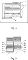
In
Aus Gründen der übersichtlicheren Darstellung sind in den Figuren keine weiteren Details der Solarzelle
Vorbereitend für einen Metallisierungsvorgang wird ein Trägersubstrat
Um die Solarzellensubstrate
Nachfolgend wird mit einem Laserstrahl
In der Metallschicht
Hierzu kann das Metall der ersten Metallschicht
Alternativ können die Eigenschaften der eingestrahlten Laserstrahlung
Wie in
In
In den
In
Es hat sich herausgestellt, dass während des Laserbondvorgangs eine solche, beispielsweise etwa 100 nm dünne Dielektrikumsschicht
Es wird darauf hingewiesen, dass eine Vielzahl unterschiedlicher Ausgestaltungen, wie erste und zweite Metallschichten
Abschließend wird darauf hingewiesen, dass in den in den Figuren dargestellten Ausführungsformen jeweils bereits an dem Solarzellensubstrat
Allerdings müssen an dem Solarzellensubstrat
Abschließend wird darauf hingewiesen, dass die Begriffe „umfassen”, „aufweisen” etc. das Vorhandensein weiterer Elemente nicht ausschließen. Der Begriff „ein” schließt auch das Vorhandensein einer Mehrzahl von Gegenständen nicht aus. Die Bezugszeichen in den Ansprüchen dienen lediglich der besseren Lesbarkeit und sollen den Schutzbereich der Ansprüche in keiner Weise einschränken.Finally, it is pointed out that the terms "comprise", "exhibit" etc. do not exclude the presence of further elements. The term "a" does not exclude the presence of a plurality of objects. The reference signs in the claims are only for better readability and are not intended to limit the scope of the claims in any way.
BezugszeichenlisteLIST OF REFERENCE NUMBERS
- 11
- Solarzellensubstratsolar cell substrate
- 22
- zweite Metallschichtsecond metal layer
- 33
- erste Metallschichtfirst metal layer
- 44
- Trägersubstratcarrier substrate
- 55
- Laserstrahlunglaser radiation
- 66
- Laserstrahlunglaser radiation
- 77
- Verbindungsbereichconnecting area
- 88th
- externe Anschlüsseexternal connections
- 99
- interne Metallverbindunginternal metal connection
- 1010
- Dielektrikumschichtdielectric
- 2020
- Solarzellesolar cell
- 100100
- Photovoltaikmodulphotovoltaic module
Claims (13)
Priority Applications (7)
| Application Number | Priority Date | Filing Date | Title |
|---|---|---|---|
| DE102011104159A DE102011104159A1 (en) | 2011-06-14 | 2011-06-14 | METHOD FOR THE ELECTRICAL CONNECTION OF SEVERAL SOLAR CELLS AND PHOTOVOLTAIC MODULE |
| US14/125,869 US20140230878A1 (en) | 2011-06-14 | 2012-06-13 | Method for electrically connecting several solar cells and photovoltaic module |
| EP12731337.7A EP2721646A1 (en) | 2011-06-14 | 2012-06-13 | Method for electrically connecting several solar cells and photovoltaic module |
| CN201280029695.5A CN103748691A (en) | 2011-06-14 | 2012-06-13 | Method for electrically connecting several solar cells and photovoltaic module |
| PCT/EP2012/061225 WO2012171968A1 (en) | 2011-06-14 | 2012-06-13 | Method for electrically connecting several solar cells and photovoltaic module |
| KR1020137033241A KR20140048884A (en) | 2011-06-14 | 2012-06-13 | Method for electrically connecting several solar cells and photovoltaic module |
| JP2014515177A JP2014519713A (en) | 2011-06-14 | 2012-06-13 | Method of electrically connecting a plurality of solar cells and photovoltaic module |
Applications Claiming Priority (1)
| Application Number | Priority Date | Filing Date | Title |
|---|---|---|---|
| DE102011104159A DE102011104159A1 (en) | 2011-06-14 | 2011-06-14 | METHOD FOR THE ELECTRICAL CONNECTION OF SEVERAL SOLAR CELLS AND PHOTOVOLTAIC MODULE |
Publications (1)
| Publication Number | Publication Date |
|---|---|
| DE102011104159A1 true DE102011104159A1 (en) | 2012-12-20 |
Family
ID=46456514
Family Applications (1)
| Application Number | Title | Priority Date | Filing Date |
|---|---|---|---|
| DE102011104159A Withdrawn DE102011104159A1 (en) | 2011-06-14 | 2011-06-14 | METHOD FOR THE ELECTRICAL CONNECTION OF SEVERAL SOLAR CELLS AND PHOTOVOLTAIC MODULE |
Country Status (7)
| Country | Link |
|---|---|
| US (1) | US20140230878A1 (en) |
| EP (1) | EP2721646A1 (en) |
| JP (1) | JP2014519713A (en) |
| KR (1) | KR20140048884A (en) |
| CN (1) | CN103748691A (en) |
| DE (1) | DE102011104159A1 (en) |
| WO (1) | WO2012171968A1 (en) |
Families Citing this family (12)
| Publication number | Priority date | Publication date | Assignee | Title |
|---|---|---|---|---|
| JP6141223B2 (en) | 2013-06-14 | 2017-06-07 | 三菱電機株式会社 | Light receiving element module and manufacturing method thereof |
| US9437756B2 (en) * | 2013-09-27 | 2016-09-06 | Sunpower Corporation | Metallization of solar cells using metal foils |
| KR101661948B1 (en) | 2014-04-08 | 2016-10-04 | 엘지전자 주식회사 | Solar cell and method for manufacturing the same |
| CN105609584B (en) * | 2014-11-19 | 2023-10-24 | 苏州易益新能源科技有限公司 | Solar cell module production method |
| KR101780564B1 (en) * | 2015-12-14 | 2017-09-21 | 한화첨단소재 주식회사 | Electrode-attached solar cell encapsulation sheet, solar cell module and manufacturing method thereof |
| US10411152B2 (en) * | 2016-06-27 | 2019-09-10 | Merlin Solar Technologies, Inc. | Solar cell bonding |
| EP3857610B1 (en) * | 2018-11-29 | 2022-07-20 | Commissariat À L'Énergie Atomique Et Aux Énergies Alternatives | Photovoltaic solar cell having information storage and display functions |
| US11978815B2 (en) | 2018-12-27 | 2024-05-07 | Solarpaint Ltd. | Flexible photovoltaic cell, and methods and systems of producing it |
| KR102583826B1 (en) * | 2019-05-24 | 2023-10-06 | 한국전자통신연구원 | Method of bonding using laser |
| CN111129224A (en) * | 2019-12-26 | 2020-05-08 | 泰州隆基乐叶光伏科技有限公司 | Production device and production method of conductive interconnection plate, and conductive interconnection plate |
| IL311089A (en) * | 2021-08-31 | 2024-04-01 | Solarpaint Ltd | Solar panels having an integral and internal metal foil, mounted on a support substrate with embedded wires |
| CN115172494A (en) * | 2022-07-01 | 2022-10-11 | 浙江爱旭太阳能科技有限公司 | IBC battery pack packaging process and IBC battery pack |
Citations (3)
| Publication number | Priority date | Publication date | Assignee | Title |
|---|---|---|---|---|
| DE3423172C2 (en) * | 1983-06-22 | 1995-08-24 | Hitachi Ltd | Method of manufacturing a solar battery |
| DE102006044936B4 (en) * | 2006-09-22 | 2008-08-07 | Fraunhofer-Gesellschaft zur Förderung der angewandten Forschung e.V. | Process for the metallization of solar cells and its use |
| WO2010027265A2 (en) * | 2008-09-05 | 2010-03-11 | Solland Solar Energy Holding B.V. | Method of monolithic photo-voltaic module assembly |
Family Cites Families (11)
| Publication number | Priority date | Publication date | Assignee | Title |
|---|---|---|---|---|
| US3411952A (en) * | 1962-04-02 | 1968-11-19 | Globe Union Inc | Photovoltaic cell and solar cell panel |
| DE2139850A1 (en) * | 1971-08-09 | 1973-02-15 | Licentia Gmbh | PROCEDURE AND EQUIPMENT FOR CONNECTING CONTACTS TO SOLAR GENERATORS |
| JPS60128647A (en) * | 1983-12-16 | 1985-07-09 | Hitachi Ltd | Flexible film conductor lead and solar battery utilizing the same |
| GB2247564B (en) * | 1990-08-16 | 1995-01-04 | Eev Ltd | A solar cell arrangement |
| DE19751487A1 (en) * | 1997-11-20 | 1999-06-02 | Pac Tech Gmbh | Method and device for the thermal connection of pads of two substrates |
| KR100638824B1 (en) * | 2005-05-20 | 2006-10-27 | 삼성전기주식회사 | Method for bonding light emitting diode chip |
| JP2008277438A (en) * | 2007-04-26 | 2008-11-13 | Ricoh Microelectronics Co Ltd | Electronic component, substrate, and method of manufacturing electronic component and substrate |
| CN101312219A (en) * | 2007-05-21 | 2008-11-26 | 国硕科技工业股份有限公司 | Solar battery |
| DE102007052972A1 (en) * | 2007-11-07 | 2009-05-14 | Solarion Ag | Method and means for joining thin metal layers |
| JP2009152249A (en) * | 2007-12-18 | 2009-07-09 | Seiko Epson Corp | Bonding method, joint structure, semiconductor device, and photoelectric conversion element |
| CN102132423A (en) * | 2008-08-27 | 2011-07-20 | 应用材料股份有限公司 | Back contact solar cell modules |
-
2011
- 2011-06-14 DE DE102011104159A patent/DE102011104159A1/en not_active Withdrawn
-
2012
- 2012-06-13 CN CN201280029695.5A patent/CN103748691A/en active Pending
- 2012-06-13 EP EP12731337.7A patent/EP2721646A1/en not_active Withdrawn
- 2012-06-13 KR KR1020137033241A patent/KR20140048884A/en active IP Right Grant
- 2012-06-13 JP JP2014515177A patent/JP2014519713A/en active Pending
- 2012-06-13 WO PCT/EP2012/061225 patent/WO2012171968A1/en active Application Filing
- 2012-06-13 US US14/125,869 patent/US20140230878A1/en not_active Abandoned
Patent Citations (3)
| Publication number | Priority date | Publication date | Assignee | Title |
|---|---|---|---|---|
| DE3423172C2 (en) * | 1983-06-22 | 1995-08-24 | Hitachi Ltd | Method of manufacturing a solar battery |
| DE102006044936B4 (en) * | 2006-09-22 | 2008-08-07 | Fraunhofer-Gesellschaft zur Förderung der angewandten Forschung e.V. | Process for the metallization of solar cells and its use |
| WO2010027265A2 (en) * | 2008-09-05 | 2010-03-11 | Solland Solar Energy Holding B.V. | Method of monolithic photo-voltaic module assembly |
Also Published As
| Publication number | Publication date |
|---|---|
| CN103748691A (en) | 2014-04-23 |
| EP2721646A1 (en) | 2014-04-23 |
| US20140230878A1 (en) | 2014-08-21 |
| WO2012171968A1 (en) | 2012-12-20 |
| KR20140048884A (en) | 2014-04-24 |
| JP2014519713A (en) | 2014-08-14 |
Similar Documents
| Publication | Publication Date | Title |
|---|---|---|
| DE102011104159A1 (en) | METHOD FOR THE ELECTRICAL CONNECTION OF SEVERAL SOLAR CELLS AND PHOTOVOLTAIC MODULE | |
| DE102007052972A1 (en) | Method and means for joining thin metal layers | |
| EP2151869A2 (en) | Semiconductor component | |
| DE102004013833A1 (en) | Solar cell element and solar cell module | |
| EP1913643A1 (en) | Solar cell module and method for its production | |
| DE102009021273A1 (en) | Method and device for producing a photovoltaic thin-film module | |
| WO2010043461A1 (en) | Method for connecting thin-film solar cells and thin-film solar module | |
| DE102013204923A1 (en) | photovoltaic module | |
| DE102011000753A1 (en) | Solar cell, solar module and method for producing a solar cell | |
| DE102011075352A1 (en) | A method of back contacting a silicon solar cell and silicon solar cell with such backside contacting | |
| EP2083445A1 (en) | Method of production of a photovoltaic modul | |
| WO2011157420A2 (en) | Method for producing a metal contact structure of a photovoltaic solar cell | |
| EP2058870A2 (en) | Contacts and module switching from thin layer solar cells to polymer carriers | |
| DE102010024307A1 (en) | Manufacturing method of metallic contact structure of e.g. metal wrap through solar cell, involves applying glass frit pastes to insulating layer on substrate, and making silver pastes to electrically contact substrate indirectly | |
| DE102008046480A1 (en) | A method for producing a solderable LFC solar cell backside and solar module interconnected from such LFC solar cells | |
| DE102013220886A1 (en) | Method for producing a metallic contacting structure on a semiconductor substrate | |
| DE102009055031A1 (en) | Back contact-solar cell for use in solar module, has perforated film and semi-conducting layer positioned on each other, and contact points whose portion is connected with conductive layer via solderless electrically conductive connection | |
| DE102011052318B4 (en) | Solar module with contact foil and solar module manufacturing process | |
| DE102011015283B4 (en) | Production of a Semiconductor Device by Laser-Assisted Bonding and Semiconductor Device Manufactured Therewith | |
| EP2254163A2 (en) | Method for manufacturing a photovoltaic module | |
| DE102016110464A1 (en) | Solar cell structure and process for producing a solar cell structure | |
| DE102017108223B4 (en) | Photovoltaic module and method for its manufacture | |
| DE102018105450A1 (en) | Process for producing a photovoltaic solar cell and photovoltaic solar cell | |
| DE102022124476A1 (en) | Solar cell module and method for producing a solar cell module | |
| DE102011051040A1 (en) | Method for manufacturing e.g. quadratic solar cell, involves back etching portion of highly doped emitter region between portions of metallization structure by using metallization structure as etching mask |
Legal Events
| Date | Code | Title | Description |
|---|---|---|---|
| R012 | Request for examination validly filed | ||
| R082 | Change of representative |
Representative=s name: QIP PATENTANWAELTE, DR. KUEHN & PARTNER MBB, DE |
|
| R119 | Application deemed withdrawn, or ip right lapsed, due to non-payment of renewal fee |