DE102011080240A1 - Singlet Harvesting with binuclear copper (I) complexes for opto-electronic devices - Google Patents
Singlet Harvesting with binuclear copper (I) complexes for opto-electronic devices Download PDFInfo
- Publication number
- DE102011080240A1 DE102011080240A1 DE102011080240A DE102011080240A DE102011080240A1 DE 102011080240 A1 DE102011080240 A1 DE 102011080240A1 DE 102011080240 A DE102011080240 A DE 102011080240A DE 102011080240 A DE102011080240 A DE 102011080240A DE 102011080240 A1 DE102011080240 A1 DE 102011080240A1
- Authority
- DE
- Germany
- Prior art keywords
- copper
- complex
- emission
- opto
- organic
- Prior art date
- Legal status (The legal status is an assumption and is not a legal conclusion. Google has not performed a legal analysis and makes no representation as to the accuracy of the status listed.)
- Withdrawn
Links
- VMQMZMRVKUZKQL-UHFFFAOYSA-N Cu+ Chemical class [Cu+] VMQMZMRVKUZKQL-UHFFFAOYSA-N 0.000 title claims abstract description 59
- 230000005693 optoelectronics Effects 0.000 title claims abstract description 25
- 238000003306 harvesting Methods 0.000 title description 11
- 239000010949 copper Substances 0.000 claims abstract description 51
- 229910052794 bromium Inorganic materials 0.000 claims abstract description 20
- 229910052801 chlorine Inorganic materials 0.000 claims abstract description 20
- 229910052740 iodine Inorganic materials 0.000 claims abstract description 20
- 239000003446 ligand Substances 0.000 claims abstract description 19
- XYFCBTPGUUZFHI-UHFFFAOYSA-N Phosphine Natural products P XYFCBTPGUUZFHI-UHFFFAOYSA-N 0.000 claims abstract description 15
- 229910000073 phosphorus hydride Inorganic materials 0.000 claims abstract description 8
- 125000000304 alkynyl group Chemical group 0.000 claims abstract description 7
- 238000000034 method Methods 0.000 claims description 22
- 125000000217 alkyl group Chemical group 0.000 claims description 17
- 229910052736 halogen Inorganic materials 0.000 claims description 15
- 150000002367 halogens Chemical group 0.000 claims description 15
- 239000002904 solvent Substances 0.000 claims description 15
- 229910052731 fluorine Inorganic materials 0.000 claims description 12
- BLRPTPMANUNPDV-UHFFFAOYSA-N Silane Chemical compound [SiH4] BLRPTPMANUNPDV-UHFFFAOYSA-N 0.000 claims description 9
- 125000001033 ether group Chemical group 0.000 claims description 9
- 125000004435 hydrogen atom Chemical group [H]* 0.000 claims description 9
- 238000006862 quantum yield reaction Methods 0.000 claims description 9
- 229910000077 silane Inorganic materials 0.000 claims description 9
- -1 alkyl radical Chemical class 0.000 claims description 8
- 238000004519 manufacturing process Methods 0.000 claims description 8
- 229910052698 phosphorus Inorganic materials 0.000 claims description 8
- 125000003118 aryl group Chemical group 0.000 claims description 7
- 229910052757 nitrogen Inorganic materials 0.000 claims description 7
- 125000004437 phosphorous atom Chemical group 0.000 claims description 7
- 125000004122 cyclic group Chemical group 0.000 claims description 6
- 125000004433 nitrogen atom Chemical group N* 0.000 claims description 6
- OKTJSMMVPCPJKN-UHFFFAOYSA-N Carbon Chemical compound [C] OKTJSMMVPCPJKN-UHFFFAOYSA-N 0.000 claims description 5
- 229910052799 carbon Inorganic materials 0.000 claims description 5
- 238000006243 chemical reaction Methods 0.000 claims description 5
- 230000003287 optical effect Effects 0.000 claims description 5
- 239000000126 substance Substances 0.000 claims description 5
- 125000001997 phenyl group Chemical group [H]C1=C([H])C([H])=C(*)C([H])=C1[H] 0.000 claims description 4
- 125000003342 alkenyl group Chemical group 0.000 claims description 3
- 150000005840 aryl radicals Chemical class 0.000 claims description 3
- 230000005669 field effect Effects 0.000 claims description 3
- 239000007789 gas Substances 0.000 claims description 3
- 125000001072 heteroaryl group Chemical group 0.000 claims description 3
- 239000003960 organic solvent Substances 0.000 claims description 3
- 239000007787 solid Substances 0.000 claims description 3
- 238000004246 ligand exchange chromatography Methods 0.000 claims description 2
- 238000002360 preparation method Methods 0.000 claims description 2
- 238000000859 sublimation Methods 0.000 claims 1
- 230000008022 sublimation Effects 0.000 claims 1
- 239000000725 suspension Substances 0.000 claims 1
- 150000003003 phosphines Chemical class 0.000 abstract 1
- 125000001424 substituent group Chemical group 0.000 description 14
- 239000010410 layer Substances 0.000 description 13
- 230000005284 excitation Effects 0.000 description 12
- 230000008569 process Effects 0.000 description 11
- 0 *c1c(*)nc[n]1* Chemical compound *c1c(*)nc[n]1* 0.000 description 8
- 229910052751 metal Inorganic materials 0.000 description 8
- 239000002184 metal Substances 0.000 description 8
- 230000007704 transition Effects 0.000 description 8
- 230000000694 effects Effects 0.000 description 7
- 239000000463 material Substances 0.000 description 7
- 150000001875 compounds Chemical class 0.000 description 5
- 229910052723 transition metal Inorganic materials 0.000 description 5
- 150000003624 transition metals Chemical class 0.000 description 5
- 238000010586 diagram Methods 0.000 description 4
- 238000000695 excitation spectrum Methods 0.000 description 4
- 230000005281 excited state Effects 0.000 description 4
- 230000005283 ground state Effects 0.000 description 4
- BASFCYQUMIYNBI-UHFFFAOYSA-N platinum Chemical compound [Pt] BASFCYQUMIYNBI-UHFFFAOYSA-N 0.000 description 4
- YMWUJEATGCHHMB-UHFFFAOYSA-N Dichloromethane Chemical compound ClCCl YMWUJEATGCHHMB-UHFFFAOYSA-N 0.000 description 3
- YXFVVABEGXRONW-UHFFFAOYSA-N Toluene Chemical compound CC1=CC=CC=C1 YXFVVABEGXRONW-UHFFFAOYSA-N 0.000 description 3
- 229910052783 alkali metal Inorganic materials 0.000 description 3
- 150000001340 alkali metals Chemical class 0.000 description 3
- 125000004429 atom Chemical group 0.000 description 3
- 239000002800 charge carrier Substances 0.000 description 3
- 230000008878 coupling Effects 0.000 description 3
- 238000010168 coupling process Methods 0.000 description 3
- 238000005859 coupling reaction Methods 0.000 description 3
- 230000005274 electronic transitions Effects 0.000 description 3
- 238000005516 engineering process Methods 0.000 description 3
- 238000002284 excitation--emission spectrum Methods 0.000 description 3
- 239000010408 film Substances 0.000 description 3
- 150000002500 ions Chemical class 0.000 description 3
- 239000011159 matrix material Substances 0.000 description 3
- 238000005259 measurement Methods 0.000 description 3
- 238000010791 quenching Methods 0.000 description 3
- 150000003254 radicals Chemical class 0.000 description 3
- 230000006798 recombination Effects 0.000 description 3
- 238000005215 recombination Methods 0.000 description 3
- QGZKDVFQNNGYKY-UHFFFAOYSA-O Ammonium Chemical compound [NH4+] QGZKDVFQNNGYKY-UHFFFAOYSA-O 0.000 description 2
- IJGRMHOSHXDMSA-UHFFFAOYSA-N Atomic nitrogen Chemical compound N#N IJGRMHOSHXDMSA-UHFFFAOYSA-N 0.000 description 2
- RTZKZFJDLAIYFH-UHFFFAOYSA-N Diethyl ether Chemical compound CCOCC RTZKZFJDLAIYFH-UHFFFAOYSA-N 0.000 description 2
- LFQSCWFLJHTTHZ-UHFFFAOYSA-N Ethanol Chemical compound CCO LFQSCWFLJHTTHZ-UHFFFAOYSA-N 0.000 description 2
- 239000005922 Phosphane Substances 0.000 description 2
- ABLZXFCXXLZCGV-UHFFFAOYSA-N Phosphorous acid Chemical compound OP(O)=O ABLZXFCXXLZCGV-UHFFFAOYSA-N 0.000 description 2
- JUJWROOIHBZHMG-UHFFFAOYSA-N Pyridine Chemical group C1=CC=NC=C1 JUJWROOIHBZHMG-UHFFFAOYSA-N 0.000 description 2
- 150000004645 aluminates Chemical class 0.000 description 2
- 150000001412 amines Chemical class 0.000 description 2
- 229940077464 ammonium ion Drugs 0.000 description 2
- 150000003863 ammonium salts Chemical class 0.000 description 2
- 150000001450 anions Chemical class 0.000 description 2
- 230000008901 benefit Effects 0.000 description 2
- 238000004364 calculation method Methods 0.000 description 2
- 125000003178 carboxy group Chemical group [H]OC(*)=O 0.000 description 2
- 239000003086 colorant Substances 0.000 description 2
- 239000013078 crystal Substances 0.000 description 2
- 238000005564 crystal structure determination Methods 0.000 description 2
- 238000005401 electroluminescence Methods 0.000 description 2
- 150000002148 esters Chemical class 0.000 description 2
- 239000010931 gold Substances 0.000 description 2
- 230000003116 impacting effect Effects 0.000 description 2
- 230000007246 mechanism Effects 0.000 description 2
- 229920002601 oligoester Polymers 0.000 description 2
- 229910000064 phosphane Inorganic materials 0.000 description 2
- 239000002798 polar solvent Substances 0.000 description 2
- 229920003229 poly(methyl methacrylate) Polymers 0.000 description 2
- 239000004926 polymethyl methacrylate Substances 0.000 description 2
- 239000000843 powder Substances 0.000 description 2
- 239000010970 precious metal Substances 0.000 description 2
- XOFYZVNMUHMLCC-ZPOLXVRWSA-N prednisone Chemical compound O=C1C=C[C@]2(C)[C@H]3C(=O)C[C@](C)([C@@](CC4)(O)C(=O)CO)[C@@H]4[C@@H]3CCC2=C1 XOFYZVNMUHMLCC-ZPOLXVRWSA-N 0.000 description 2
- 230000000171 quenching effect Effects 0.000 description 2
- 238000001228 spectrum Methods 0.000 description 2
- 150000003462 sulfoxides Chemical class 0.000 description 2
- BUHVIAUBTBOHAG-FOYDDCNASA-N (2r,3r,4s,5r)-2-[6-[[2-(3,5-dimethoxyphenyl)-2-(2-methylphenyl)ethyl]amino]purin-9-yl]-5-(hydroxymethyl)oxolane-3,4-diol Chemical compound COC1=CC(OC)=CC(C(CNC=2C=3N=CN(C=3N=CN=2)[C@H]2[C@@H]([C@H](O)[C@@H](CO)O2)O)C=2C(=CC=CC=2)C)=C1 BUHVIAUBTBOHAG-FOYDDCNASA-N 0.000 description 1
- XEXYRTTUCDBSPJ-UHFFFAOYSA-N (6-methylpyridin-2-yl)-diphenylphosphane Chemical compound CC1=CC=CC(P(C=2C=CC=CC=2)C=2C=CC=CC=2)=N1 XEXYRTTUCDBSPJ-UHFFFAOYSA-N 0.000 description 1
- JWUJQDFVADABEY-UHFFFAOYSA-N 2-methyltetrahydrofuran Chemical compound CC1CCCO1 JWUJQDFVADABEY-UHFFFAOYSA-N 0.000 description 1
- RYGMFSIKBFXOCR-UHFFFAOYSA-N Copper Chemical group [Cu] RYGMFSIKBFXOCR-UHFFFAOYSA-N 0.000 description 1
- AVXURJPOCDRRFD-UHFFFAOYSA-N Hydroxylamine Chemical compound ON AVXURJPOCDRRFD-UHFFFAOYSA-N 0.000 description 1
- 241000530268 Lycaena heteronea Species 0.000 description 1
- OAICVXFJPJFONN-UHFFFAOYSA-N Phosphorus Chemical compound [P] OAICVXFJPJFONN-UHFFFAOYSA-N 0.000 description 1
- 239000004721 Polyphenylene oxide Substances 0.000 description 1
- 229910018557 Si O Inorganic materials 0.000 description 1
- 230000006978 adaptation Effects 0.000 description 1
- 125000003158 alcohol group Chemical group 0.000 description 1
- 150000001338 aliphatic hydrocarbons Chemical class 0.000 description 1
- 125000006193 alkinyl group Chemical group 0.000 description 1
- 230000005540 biological transmission Effects 0.000 description 1
- 230000015572 biosynthetic process Effects 0.000 description 1
- 230000000903 blocking effect Effects 0.000 description 1
- 150000001642 boronic acid derivatives Chemical class 0.000 description 1
- KVNRLNFWIYMESJ-UHFFFAOYSA-N butyronitrile Chemical compound CCCC#N KVNRLNFWIYMESJ-UHFFFAOYSA-N 0.000 description 1
- 125000002915 carbonyl group Chemical group [*:2]C([*:1])=O 0.000 description 1
- 150000001732 carboxylic acid derivatives Chemical class 0.000 description 1
- 150000001768 cations Chemical class 0.000 description 1
- 230000008859 change Effects 0.000 description 1
- 238000012512 characterization method Methods 0.000 description 1
- 238000004590 computer program Methods 0.000 description 1
- 239000004020 conductor Substances 0.000 description 1
- 150000001879 copper Chemical class 0.000 description 1
- 229910052802 copper Inorganic materials 0.000 description 1
- 230000009849 deactivation Effects 0.000 description 1
- 230000003247 decreasing effect Effects 0.000 description 1
- 238000009792 diffusion process Methods 0.000 description 1
- 239000006185 dispersion Substances 0.000 description 1
- 238000004090 dissolution Methods 0.000 description 1
- 238000009826 distribution Methods 0.000 description 1
- 238000000295 emission spectrum Methods 0.000 description 1
- 238000005265 energy consumption Methods 0.000 description 1
- 230000007613 environmental effect Effects 0.000 description 1
- 238000001914 filtration Methods 0.000 description 1
- 238000002189 fluorescence spectrum Methods 0.000 description 1
- 239000011521 glass Substances 0.000 description 1
- PCHJSUWPFVWCPO-UHFFFAOYSA-N gold Chemical compound [Au] PCHJSUWPFVWCPO-UHFFFAOYSA-N 0.000 description 1
- 229910052737 gold Inorganic materials 0.000 description 1
- 150000002443 hydroxylamines Chemical class 0.000 description 1
- AMGQUBHHOARCQH-UHFFFAOYSA-N indium;oxotin Chemical compound [In].[Sn]=O AMGQUBHHOARCQH-UHFFFAOYSA-N 0.000 description 1
- 238000007641 inkjet printing Methods 0.000 description 1
- 229910052741 iridium Inorganic materials 0.000 description 1
- GKOZUEZYRPOHIO-UHFFFAOYSA-N iridium atom Chemical compound [Ir] GKOZUEZYRPOHIO-UHFFFAOYSA-N 0.000 description 1
- 231100001231 less toxic Toxicity 0.000 description 1
- 239000004973 liquid crystal related substance Substances 0.000 description 1
- 238000004020 luminiscence type Methods 0.000 description 1
- 239000013212 metal-organic material Substances 0.000 description 1
- 150000002739 metals Chemical class 0.000 description 1
- 125000002496 methyl group Chemical group [H]C([H])([H])* 0.000 description 1
- 238000004776 molecular orbital Methods 0.000 description 1
- 229910000510 noble metal Inorganic materials 0.000 description 1
- 239000012454 non-polar solvent Substances 0.000 description 1
- 239000012044 organic layer Substances 0.000 description 1
- 230000003647 oxidation Effects 0.000 description 1
- 238000007254 oxidation reaction Methods 0.000 description 1
- 150000004714 phosphonium salts Chemical class 0.000 description 1
- 238000001296 phosphorescence spectrum Methods 0.000 description 1
- 239000011574 phosphorus Substances 0.000 description 1
- 229910052697 platinum Inorganic materials 0.000 description 1
- 229920002627 poly(phosphazenes) Polymers 0.000 description 1
- 229920000570 polyether Polymers 0.000 description 1
- 229920000642 polymer Polymers 0.000 description 1
- 229920001296 polysiloxane Polymers 0.000 description 1
- 239000002244 precipitate Substances 0.000 description 1
- 239000002243 precursor Substances 0.000 description 1
- 230000002265 prevention Effects 0.000 description 1
- UMJSCPRVCHMLSP-UHFFFAOYSA-N pyridine Natural products COC1=CC=CN=C1 UMJSCPRVCHMLSP-UHFFFAOYSA-N 0.000 description 1
- 239000011541 reaction mixture Substances 0.000 description 1
- 230000004044 response Effects 0.000 description 1
- 230000000630 rising effect Effects 0.000 description 1
- 150000003839 salts Chemical class 0.000 description 1
- 238000007650 screen-printing Methods 0.000 description 1
- 150000004756 silanes Chemical class 0.000 description 1
- LIVNPJMFVYWSIS-UHFFFAOYSA-N silicon monoxide Inorganic materials [Si-]#[O+] LIVNPJMFVYWSIS-UHFFFAOYSA-N 0.000 description 1
- 239000011877 solvent mixture Substances 0.000 description 1
- 230000006641 stabilisation Effects 0.000 description 1
- 238000011105 stabilization Methods 0.000 description 1
- 230000000087 stabilizing effect Effects 0.000 description 1
- 125000000547 substituted alkyl group Chemical group 0.000 description 1
- 238000006467 substitution reaction Methods 0.000 description 1
- 230000001629 suppression Effects 0.000 description 1
- 239000010409 thin film Substances 0.000 description 1
- 150000003568 thioethers Chemical class 0.000 description 1
- 230000009466 transformation Effects 0.000 description 1
- 238000007704 wet chemistry method Methods 0.000 description 1
- 238000012982 x-ray structure analysis Methods 0.000 description 1
Images


Classifications
-
- H—ELECTRICITY
- H10—SEMICONDUCTOR DEVICES; ELECTRIC SOLID-STATE DEVICES NOT OTHERWISE PROVIDED FOR
- H10K—ORGANIC ELECTRIC SOLID-STATE DEVICES
- H10K71/00—Manufacture or treatment specially adapted for the organic devices covered by this subclass
-
- C—CHEMISTRY; METALLURGY
- C09—DYES; PAINTS; POLISHES; NATURAL RESINS; ADHESIVES; COMPOSITIONS NOT OTHERWISE PROVIDED FOR; APPLICATIONS OF MATERIALS NOT OTHERWISE PROVIDED FOR
- C09K—MATERIALS FOR MISCELLANEOUS APPLICATIONS, NOT PROVIDED FOR ELSEWHERE
- C09K11/00—Luminescent, e.g. electroluminescent, chemiluminescent materials
- C09K11/06—Luminescent, e.g. electroluminescent, chemiluminescent materials containing organic luminescent materials
-
- C—CHEMISTRY; METALLURGY
- C07—ORGANIC CHEMISTRY
- C07F—ACYCLIC, CARBOCYCLIC OR HETEROCYCLIC COMPOUNDS CONTAINING ELEMENTS OTHER THAN CARBON, HYDROGEN, HALOGEN, OXYGEN, NITROGEN, SULFUR, SELENIUM OR TELLURIUM
- C07F9/00—Compounds containing elements of Groups 5 or 15 of the Periodic Table
- C07F9/02—Phosphorus compounds
- C07F9/547—Heterocyclic compounds, e.g. containing phosphorus as a ring hetero atom
- C07F9/553—Heterocyclic compounds, e.g. containing phosphorus as a ring hetero atom having one nitrogen atom as the only ring hetero atom
- C07F9/576—Six-membered rings
- C07F9/58—Pyridine rings
-
- H—ELECTRICITY
- H10—SEMICONDUCTOR DEVICES; ELECTRIC SOLID-STATE DEVICES NOT OTHERWISE PROVIDED FOR
- H10K—ORGANIC ELECTRIC SOLID-STATE DEVICES
- H10K50/00—Organic light-emitting devices
- H10K50/10—OLEDs or polymer light-emitting diodes [PLED]
- H10K50/11—OLEDs or polymer light-emitting diodes [PLED] characterised by the electroluminescent [EL] layers
-
- H—ELECTRICITY
- H10—SEMICONDUCTOR DEVICES; ELECTRIC SOLID-STATE DEVICES NOT OTHERWISE PROVIDED FOR
- H10K—ORGANIC ELECTRIC SOLID-STATE DEVICES
- H10K85/00—Organic materials used in the body or electrodes of devices covered by this subclass
- H10K85/30—Coordination compounds
- H10K85/361—Polynuclear complexes, i.e. complexes comprising two or more metal centers
-
- H—ELECTRICITY
- H10—SEMICONDUCTOR DEVICES; ELECTRIC SOLID-STATE DEVICES NOT OTHERWISE PROVIDED FOR
- H10K—ORGANIC ELECTRIC SOLID-STATE DEVICES
- H10K85/00—Organic materials used in the body or electrodes of devices covered by this subclass
- H10K85/30—Coordination compounds
- H10K85/371—Metal complexes comprising a group IB metal element, e.g. comprising copper, gold or silver
-
- C—CHEMISTRY; METALLURGY
- C09—DYES; PAINTS; POLISHES; NATURAL RESINS; ADHESIVES; COMPOSITIONS NOT OTHERWISE PROVIDED FOR; APPLICATIONS OF MATERIALS NOT OTHERWISE PROVIDED FOR
- C09K—MATERIALS FOR MISCELLANEOUS APPLICATIONS, NOT PROVIDED FOR ELSEWHERE
- C09K2211/00—Chemical nature of organic luminescent or tenebrescent compounds
- C09K2211/18—Metal complexes
- C09K2211/188—Metal complexes of other metals not provided for in one of the previous groups
-
- H—ELECTRICITY
- H10—SEMICONDUCTOR DEVICES; ELECTRIC SOLID-STATE DEVICES NOT OTHERWISE PROVIDED FOR
- H10K—ORGANIC ELECTRIC SOLID-STATE DEVICES
- H10K2101/00—Properties of the organic materials covered by group H10K85/00
- H10K2101/10—Triplet emission
-
- Y—GENERAL TAGGING OF NEW TECHNOLOGICAL DEVELOPMENTS; GENERAL TAGGING OF CROSS-SECTIONAL TECHNOLOGIES SPANNING OVER SEVERAL SECTIONS OF THE IPC; TECHNICAL SUBJECTS COVERED BY FORMER USPC CROSS-REFERENCE ART COLLECTIONS [XRACs] AND DIGESTS
- Y02—TECHNOLOGIES OR APPLICATIONS FOR MITIGATION OR ADAPTATION AGAINST CLIMATE CHANGE
- Y02E—REDUCTION OF GREENHOUSE GAS [GHG] EMISSIONS, RELATED TO ENERGY GENERATION, TRANSMISSION OR DISTRIBUTION
- Y02E10/00—Energy generation through renewable energy sources
- Y02E10/50—Photovoltaic [PV] energy
- Y02E10/549—Organic PV cells
Landscapes
- Chemical & Material Sciences (AREA)
- Engineering & Computer Science (AREA)
- Materials Engineering (AREA)
- Organic Chemistry (AREA)
- Inorganic Chemistry (AREA)
- Physics & Mathematics (AREA)
- Biochemistry (AREA)
- General Health & Medical Sciences (AREA)
- Molecular Biology (AREA)
- Manufacturing & Machinery (AREA)
- Life Sciences & Earth Sciences (AREA)
- High Energy & Nuclear Physics (AREA)
- Health & Medical Sciences (AREA)
- Optics & Photonics (AREA)
- Electroluminescent Light Sources (AREA)
Abstract
Die Erfindung betrifft dimere Kupfer(I)-Komplexe, insbesondere als Emitter in optoelektronischen Vorrichtungen wie organische lichtemittierende Dioden (OLEDs) und andere Bauelemente, gemäß Formel AFormel A worin bedeutet: Cu: Cu(I), X: Cl, Br, I, SCN, CN, und/oder Alkinyl und P∩N: ein mit einem N-Heterocyclus subtituierter Phosphanligand.The invention relates to dimeric copper (I) complexes, in particular as emitters in optoelectronic devices such as organic light-emitting diodes (OLEDs) and other components, according to formula AFormel A in which: Cu: Cu (I), X: Cl, Br, I, SCN, CN, and / or alkynyl and P∩N: an N-heterocycle-substituted phosphine ligand.
Description
Die vorliegende Erfindung betrifft neuartige dimere Kupfer(I)-Komplexe und deren Verwendung, insbesondere als Emitter in opto-elektronischen Vorrichtungen wie organischen lichtemittierenden Dioden (OLEDs) und anderen.The present invention relates to novel dimeric copper (I) complexes and their use, in particular as emitters in opto-electronic devices such as organic light-emitting diodes (OLEDs) and others.
Hintergrundbackground
Zur Zeit setzen sich im Bereich der Bildschirm- und Licht-Technik neue Verfahren durch. Es wird möglich sein, flache Displays oder Leuchtflächen mit einer Dicke von unter 0,5 mm zu fertigen. Diese sind durch viele faszinierende Eigenschaften ausgezeichnet. So werden z. B. Leuchtflächen als Tapeten mit sehr geringem Energieverbrauch realisierbar sein. Besonders interessant ist auch, dass Farbbildschirme mit bisher nicht erreichbarer Farb-Echtheit, Helligkeit und Blickwinkelunabhängigkeit, mit geringem Gewicht sowie sehr niedrigem Stromverbrauch herstellbar sein werden. Die Bildschirme werden sich als Mikro-Displays oder Großbildschirme mit mehreren Quadratmetern Fläche in starrer Form oder flexibel, aber auch als Transmissions- oder Reflexions-Displays gestalten lassen. Ferner wird es möglich sein, einfache und kostensparende Herstellungsverfahren wie Siebdruck oder Tintenstrahldruck einzusetzen. Dadurch wird im Vergleich zu herkömmlichen Flachbildschirmen eine sehr preiswerte Fertigung ermöglicht. Diese neue Technik basiert auf dem Prinzip der OLEDs, den „Organic Light Emitting Diodes”. Darüber hinaus zeichnen sich durch die Verwendung spezieller metall-organischer Materialien (Moleküle) viele neue optoelektronische Anwendungen, z. B. im Bereich organischer Solarzelle, organischer Feldeffekttransistoren, organischer Photodioden usw. ab.At the moment, new procedures are being implemented in the field of screen and lighting technology. It will be possible to produce flat displays or illuminated areas with a thickness of less than 0.5 mm. These are distinguished by many fascinating properties. So z. B. lighting surfaces can be realized as wallpaper with very low energy consumption. It is also particularly interesting that color screens with previously unachievable color authenticity, brightness and viewing angle independence, with low weight and very low power consumption will be produced. The screens can be designed as micro-displays or large screens with several square meters of surface in rigid form or flexible, but also as transmission or reflection displays. Furthermore, it will be possible to use simple and cost-saving production methods such as screen printing or inkjet printing. As a result, a very inexpensive production is possible compared to conventional flat screens. This new technology is based on the principle of OLEDs, the "Organic Light Emitting Diodes". In addition, the use of special metal-organic materials (molecules) many new optoelectronic applications, eg. As in the field of organic solar cell, organic field effect transistors, organic photodiodes, etc. from.
So lässt sich besonders für den OLED-Bereich erkennen, dass derartige Anordnungen bereits jetzt wirtschaftlich bedeutend sind, da eine Massenfertigung von OLED-Handy-Displays bereits aufgenommen wurde. Derartige OLEDs bestehen vorwiegend aus organischen Schichten, die auch flexibel und kostengünstig zu fertigen sind. Hervorzuheben ist, dass sich OLED-Bauelemente großflächig als Beleuchtungskörper, aber auch klein als Pixels für Displays gestalten gestalten lassen.Thus, it can be seen, especially for the OLED field, that such arrangements are already economically significant, since a mass production of OLED mobile phone displays has already been started. Such OLEDs consist predominantly of organic layers, which are also flexible and inexpensive to manufacture. It should be emphasized that OLED components can be designed over a large area as lighting fixtures, but also as small pixels for displays.
Gegenüber herkömmlichen Technologien, wie etwa Flüssigkristall-Displays (LCDs), Plasma-Displays oder Kathodenstrahlenröhren (CRTs) weisen OLEDs zahlreiche Vorteile auf, wie eine geringe Betriebsspannung von einigen Volt, eine dünne Struktur von einigen hundert nm, hoch-effizient selbst-leuchtende Pixel, einen hohen Kontrast und eine gute Auflösung sowie die Möglichkeit, alle Farben darzustellen. Weiterhin wird in einem OLED Licht beim Anliegen elektrischer Spannung direkt erzeugt, anstelle es nur zu modulieren.Compared to conventional technologies, such as liquid crystal displays (LCDs), plasma displays or cathode ray tubes (CRTs), OLEDs have numerous advantages, such as a low operating voltage of a few volts, a thin structure of several hundred nm, high-efficiency self-luminous pixels , a high contrast and a good resolution as well as the possibility to display all colors. Furthermore, in an OLED light is generated directly when applying electrical voltage, instead of only modulating it.
Einen Überblick über die Funktion von OLEDs findet sich beispielsweise bei
Seit den ersten Berichten über OLEDs (siehe z. B.
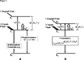
OLEDs werden in der Regel in Schichtenstrukturen realisiert. Zum besseren Verständnis ist in
Als elektronischer Anregungszustand, der auch durch Energieübertragung von einem geeigneten Vorläufer-Exziton gebildet werden kann, kommt, von wenigen Ausnahmen abgesehen, entweder ein Singulett- oder ein Triplett-Zustand, bestehend aus drei Unterzuständen, in Betracht. Da beide Zustände aufgrund der Spinstatistik in der Regel im Verhältnis 1:3 besetzt werden, ergibt sich, dass bei einer Emission aus dem Singulett-Zustand, die als Fluoreszenz bezeichnet wird, nur maximal 25% der erzeugten Exzitonen wieder zur Emission führen. Dagegen können bei einer Triplett-Emission, die als Phosphoreszenz bezeichnet wird, sämtliche Exzitonen ausgenutzt, umgewandelt und als Licht emittiert werden (Triplett-Harvesting), so dass in diesem Fall die Innere Quantenausbeute den Wert von 100% erreichen kann, sofern der mit angeregte und energetisch über dem Triplett-Zustand liegende Singulett-Zustand vollständig in den Triplett-Zustand relaxiert (Inter-System-Crossing, ISC) und strahlungslose Konkurrenzprozesse bedeutungslos bleiben. Somit sind Triplett-Emitter nach dem bisherigen Stand der Technik effizientere Elektro-Luminophore und besser geeignet, in einer organischen Leuchtdiode für eine hohe Lichtausbeute zu sorgen.As an electronic excitation state, which can also be formed by energy transfer from a suitable precursor exciton, there is, with a few exceptions, either a singleton or a triplet state consisting of three sub-states, into consideration. Since both states are usually occupied in a ratio of 1: 3 due to the spin statistics, it follows that for an emission from the singlet state, which is referred to as fluorescence, only a maximum of 25% of the excitons produced lead to emission again. In contrast, in a triplet emission, which is referred to as phosphorescence, all excitons are exploited, converted and emitted as light (triplet harvesting), so that in this case the internal quantum efficiency can reach the value of 100%, if the excited with and energetically over the triplet state singlet state completely relaxed in the triplet state (inter-system crossing, ISC) and radiationless competition processes remain meaningless. Thus, prior art triplet emitters are more efficient electro-luminophores and more suitable for providing high light output in an organic light emitting diode.
Bei den für das Triplett-Harvesting geeigneten Triplett-Emittern werden in der Regel Übergangsmetall-Komplexverbindungen eingesetzt, in denen das Metall aus der dritten Periode der Übergangsmetalle gewählt wird. Hierbei handelt es sich vorwiegend um sehr teure Edelmetalle wie Iridium, Platin oder auch Gold (siehe dazu auch
Es wäre von großem wirtschaftlichem Vorteil, wenn diese teuren Edelmetalle durch preiswerte Metalle ersetzt werden könnten. Darüber hinaus ist eine Vielzahl der bisher bekannten OLED-Emitter-Materialien aus ökologischer Sicht nicht unbedenklich, so dass die Verwendung von weniger toxischen Materialien wünschenswert wäre. Hierfür kämen z. B. Kupfer(I)-Komplexe in Betracht. Allerdings weisen diese eine wesentlich geringere SBK auf (SBK-Konstanten von Cu(I): ≈ 850 cm–1, Ref.:
Darüber hinaus erfolgen in der Regel in Cu(I)-Komplexen nach dem Anregungsprozess (durch Elektron-Loch-Rekombination oder durch optische Anregung) ausgeprägte Geometrie-Veränderungen, wodurch die Emissionsquantenausbeuten stark reduziert werden. Ferner werden durch diese Prozesse die Emissionsfarben in unerwünschter Weise rot-verschoben.In addition, pronounced geometry changes generally occur in Cu (I) complexes after the excitation process (by electron-hole recombination or by optical excitation), whereby the emission quantum yields are greatly reduced. Furthermore, the emission colors are undesirably red-shifted by these processes.
Es ist Ziel dieser Erfindung, neue Materialien bereitzustellen, die die oben genannten Nachteile nicht aufweisen.It is an object of this invention to provide new materials that do not have the disadvantages mentioned above.
Kurze Beschreibung der ErfindungBrief description of the invention
Überraschender Weise wird das Ziel der Erfindung durch Kupfer(I)-Komplexe (Cu(I)-Komplexe) erreicht, die zur Emission von Licht fähig sind und eine Struktur gemäß Formel A aufweisen 
In Formel A bedeutet
Cu: Cu(I);
X: Cl, Br, I, SCN, CN, und/oder Alkinyl (R*–≡) (R* ist definiert wie R);
P∩N: ein mit einem N-Heterocyclus substituierter Phosphanligand, insbesondere mit einer Struktur gemäß Formel B 
E: ein Kohlenstoff- oder Stickstoffatom;
E': ein Kohlenstoff- oder Stickstoffatom, das nicht mit einem Wasserstoffatom substituiert ist;
gestrichelte Bindung: eine Einfach- oder Doppelbindung;
R: Alkyl-Rest [CH3-(CH2)n-] (n = 0–20), optional verzweigt oder mit Halogenen (F, Cl, Br, I) substituiert, oder
Aryl-Rest (insbesondere Phenyl), optional mit Alkyl-Gruppen, Halogenen (F, Cl, Br, I), Silan-(-SiR*3) (R* definiert wie R1 unten) oder Ethergruppen -OR** (R** definiert wie R1 unten) substituiert,
ungesättigte Gruppe, wie z. B. Alkenyl- und Alkinyl-Gruppen, optional mit Alkyl-Gruppen, Halogenen (F, Cl, Br, I), Silan-(-SiR***3) oder Ethergruppen -OR*** (R*** definiert wie R1 unten) substituiert, wobei R kein Wasserstoffatom ist;
R', R'': Alkyl-Gruppen [CH3-(CH2)n-] (n = 0–20, bevorzugt n > 6), die auch verzweigt oder cyclisch sein können, oder
Aryl- oder Heteroarylgruppen, die optional mit Alkyl-Gruppen, Halogenen (F, Cl, Br, I), Silan-(-SiR*3) oder Ethergruppen -OR* (R* definiert wie R1) substituiert sind,
wobei R' und R'' jeweils direkt an dem Phosphoratom des Phosphan-Liganden gebunden sind;
R1: definiert wie R, wobei R1 optional ein Wasserstoffatom ist;
wobei R, R1 optional annelierte Ringsysteme bilden können.In formula A means
Cu: Cu (I);
X: Cl, Br, I, SCN, CN, and / or alkynyl (R * -≡) (R * is defined as R);
P∩N: a substituted with an N-heterocycle phosphine ligand, in particular having a structure according to formula B.
E: a carbon or nitrogen atom;
E ': a carbon or nitrogen atom which is not substituted with a hydrogen atom;
dashed bond: a single or double bond;
R: alkyl radical [CH 3 - (CH 2 ) n -] (n = 0-20), optionally branched or substituted by halogens (F, Cl, Br, I), or
Aryl radical (especially phenyl), optionally with alkyl groups, halogens (F, Cl, Br, I), silane - (- SiR * 3 ) (R * defined as R1 below) or ether groups -OR ** (R * * defined as R1 below) substituted,
unsaturated group, such as. Alkenyl and alkynyl groups, optionally with alkyl groups, halogens (F, Cl, Br, I), silane - (- SiR *** 3 ) or ether groups --OR *** (R *** defines R1 below), where R is not a hydrogen atom;
R ', R ": alkyl groups [CH 3 - (CH 2 ) n -] (n = 0-20, preferably n> 6), which may also be branched or cyclic, or
Aryl or heteroaryl groups which are optionally substituted by alkyl groups, halogens (F, Cl, Br, I), silane - (- SiR * 3 ) or ether groups --OR * (R * defined as R1),
wherein R 'and R "are each directly attached to the phosphorus atom of the phosphane ligand;
R1: defines as R, wherein R1 is optionally a hydrogen atom;
where R, R1 can optionally form fused ring systems.
In einer bevorzugten Ausführungsform der Erfindung erhöhen R, R1, R' und/oder R' (sowie die weiter unten definierten Reste R2 und/oder R3) die Löslichkeit des Kupfer(I)komplexes in organischen Lösungsmitteln. Diese Substituenten können auch die Loch- oder die Elektronenleitung des Komplexes erhöhen. Entsprechende Loch- und Elektronenleiter sind dem Fachmann bekannt.In a preferred embodiment of the invention, R, R1, R 'and / or R' (and the radicals R2 and / or R3 defined below) increase the solubility of the copper (I) complex in organic solvents. These substituents can also increase the hole or electron conduction of the complex. Corresponding hole and electron conductors are known to the person skilled in the art.
Weiterhin betrifft die Erfindung einen Kupfer(I)-Komplex, der einen ΔE-Abstand zwischen dem untersten Triplett-Zustand und dem darüber liegenden Singulett-Zustand (ΔE(S1 – T1)-Wert) von 50 cm–1 bis kleiner als 2000 cm–1, bevorzugt bis kleiner als 1500 cm–1, mehr bevorzugt bis kleiner als 1000 cm–1, besonders bevorzugt bis kleiner als 500 cm–1 aufweist. Ein derartiger Kupfer(I)-Komplex hat eine Struktur gemäß Formel A, ohne auf diese Struktur beschränkt zu sein.Furthermore, the invention relates to a copper (I) complex having a ΔE distance between the lowest triplet state and the overlying singlet state (ΔE (S 1 -T 1 ) value) of 50 cm -1 to less than 2000 cm -1 , preferably to less than 1500 cm -1 , more preferably to less than 1000 cm -1 , more preferably to less than 500 cm -1 . Such a copper (I) complex has a structure according to formula A without being limited to this structure.
Bevorzugt weist der Kupfer(I)-Komplex eine Emissionsquantenausbeute von größer 40%, bevorzugt größer 60%, besonders bevorzugt größer 70% auf, am meisten bevorzugt von größer 90% auf. Bevorzugt weist der Kupfer(I)-Komplex eine Emissionslebensdauer von höchstens 10 μs, bevorzugt kleiner 6 μs, besonders bevorzugt kleiner 3 μs auf. Bevorzugt weist der Kupfer(I)-Komplex eine Löslichkeit in organischen Lösungsmitteln von mindestens 10 g/l auf. The copper (I) complex preferably has an emission quantum yield of greater than 40%, preferably greater than 60%, particularly preferably greater than 70%, most preferably greater than 90%. The copper (I) complex preferably has an emission lifetime of at most 10 μs, preferably less than 6 μs, particularly preferably less than 3 μs. The copper (I) complex preferably has a solubility in organic solvents of at least 10 g / l.
In einem weiteren Aspekt betrifft die Erfindung die Verwendung eines Kupfer(I)-Komplexes der genannten Art zur Emission von Licht, insbesondere in einer Emitterschicht in einer optoelektronischen Vorrichtung.In a further aspect, the invention relates to the use of a copper (I) complex of the type mentioned for the emission of light, in particular in an emitter layer in an optoelectronic device.
In einem weiteren Aspekt betrifft die Erfindung ein Verfahren zur Herstellung einer optoelektronischen Vorrichtung, wobei ein Kupfer(I)-Komplex der genannten Art verwendet wird.In a further aspect, the invention relates to a method for producing an optoelectronic device, wherein a copper (I) complex of the type mentioned is used.
Bevorzugt weist das Herstellungsverfahren nass-chemische Schritte auf, insbesondere die Aufbringung eines in einem ersten Lösungsmittel gelösten ersten Kupfer(I)-Komplexes auf einen festen Träger, und die Aufbringung eines in einem zweiten Lösungsmittel gelösten zweiten Kupfer(I)-Komplexes auf den Träger. Dabei ist der erste Kupfer(I)-Komplex nicht in dem zweiten Lösungsmittel löslich ist und der zweite Kupfer(I)-Komplex nicht in dem ersten Lösungsmittel löslich. Der erste Kupfer(I)-Komplex und/oder der zweite Kupfer(I)-Komplex sind bevorzugt ein Kupfer(I)-Komplex nach Formel A.The production process preferably comprises wet-chemical steps, in particular the application of a first copper (I) complex dissolved in a first solvent to a solid support, and the application of a second copper (I) complex dissolved in a second solvent onto the support , In this case, the first copper (I) complex is not soluble in the second solvent and the second copper (I) complex is not soluble in the first solvent. The first copper (I) complex and / or the second copper (I) complex are preferably a copper (I) complex according to formula A.
Wenn der Kupfer(I)-Komplex keine ausreichende Löslichkeit aufweist, kann die Verarbeitung des Komplexes auch als Dispersion erfolgen.If the copper (I) complex does not have sufficient solubility, the complex may also be processed as a dispersion.
Optional kann das Verfahren weiterhin den Schritt der Aufbringung eines in dem ersten Lösungsmittel oder in einem dritten Lösungsmittel gelösten dritten Kupfer(I)-Komplexes auf den festen Träger auf, wobei der dritte Kupfer(I)-Komplex ein Kupfer(I)-Komplex nach Formel A ist. In einer bevorzugten Ausführungsform ist die opto-elektronische Vorrichtung eine Weißlicht-OLED, wobei der erste Kupfer(I)-Komplex ein Rotlichtemitter ist, der zweite Kupfer(I)-Komplex ein Grünlichtemitter ist und der dritte Kupfer(I)-Komplex ein Blaulichtemitter ist.Optionally, the method may further comprise the step of applying a third copper (I) complex dissolved in the first solvent or in a third solvent to the solid support, wherein the third copper (I) complex comprises a copper (I) complex Formula A is. In a preferred embodiment, the optoelectronic device is a white light OLED wherein the first copper (I) complex is a red light emitter, the second copper (I) complex is a green light emitter, and the third copper (I) complex is a blue light emitter is.
In einem weiteren Aspekt betrifft die Erfindung eine opto-elektronische Vorrichtung aufweisend einen zweikernigen Kupfer(I)-Komplex, der einen ΔE-Abstand zwischen dem untersten Triplett-Zustand und dem darüber liegenden Singulett-Zustand zwischen 50 cm–1 und 2500 cm–1, bevorzugt zwischen 50 cm–1 und 2000 cm–1, bevorzugt zwischen 50 cm–1 und 1000 cm–1, besonders bevorzugt zwischen 50 cm–1 und 500 cm–1 aufweist. Eine derartige optoelektronische Vorrichtung weist insbesondere einen Kupfer(I)-Komplex nach Formel A auf.In another aspect, the invention relates to an optoelectronic device comprising a dinuclear copper (I) complex having a ΔE distance between the lowest triplet state and the overlying singlet state between 50 cm -1 and 2500 cm -1 , preferably between 50 cm -1 and 2000 cm -1 , preferably between 50 cm -1 and 1000 cm -1 , particularly preferably between 50 cm -1 and 500 cm -1 . Such an optoelectronic device has in particular a copper (I) complex according to formula A.
In einer solchen opto-elektronischen Vorrichtung beträgt der Anteil des Kupfer(I)-Komplexes in einer Emitterschicht der Vorrichtung 2 bis 100 Gew.-%, bevorzugt 30 bis 100 Gew.-%, bezogen auf das Gesamtgewicht der Emitterschicht. Sofern die opto-elektronische Vorrichtung in Form einer organischen Leuchtdiode (OLED) vorliegt, weist die Emitterschicht bevorzugt einen Kupfer(I)-Komplex Formel A in der Emitterschicht auf, wobei der Anteil des Kupfer(I)-Komplexes in der Emitterschicht zwischen 2 bis 100 Gew.-%, bevorzugt 30 bis 100 Gew.-%, bezogen auf das Gesamtgewicht der Emitterschicht, beträgt.In such an optoelectronic device, the proportion of the copper (I) complex in an emitter layer of the device is 2 to 100% by weight, preferably 30 to 100% by weight, based on the total weight of the emitter layer. If the optoelectronic device is in the form of an organic light emitting diode (OLED), the emitter layer preferably has a copper (I) complex formula A in the emitter layer, wherein the proportion of the copper (I) complex in the emitter layer is between 2 to 100 wt .-%, preferably 30 to 100 wt .-%, based on the total weight of the emitter layer is.
Der Begriff „opto-elektronische Vorrichtung” bezieht sich vor allem auf organische Leuchtidioden (OLEDs), lichtemittierende elektrochemische Zellen (LEECs oder LECs), OLED-Sensoren, insbesondere nicht hermetisch nach außen abgeschirmten Gas- und Dampf-Sensoren, optische Temperatur-Sensoren, organische Solarzellen (OSCs), organische Feldeffekttransistoren, organische Lasern, organischen Dioden, organischen Photodioden und „down conversion” Systeme.The term "opto-electronic device" refers above all to organic light-emitting diodes (OLEDs), light-emitting electrochemical cells (LEECs or LECs), OLED sensors, in particular non-hermetically shielded gas and vapor sensors, optical temperature sensors, organic solar cells (OSCs), organic field effect transistors, organic lasers, organic diodes, organic photodiodes, and down conversion systems.
Ausführliche Beschreibung der ErfindungDetailed description of the invention
Überraschender Weise wird das oben genannte Ziel der Erfindung durch die hier beschriebenen Kupfer(I)-Komplexe (Cu(I)-Komplexe) erreicht. Das heißt, die Erfindung betrifft die Schaffung und Bereitstellung und Verwendung von Cu(I)-Verbindungen, die insbesondere folgende Eigenschaften zeigen:
- – relativ kurze Emissionslebensdauer von nur wenigen μs,
- – hohe Emissionsquantenausbeuten größer
als 40%, bevorzugt von größer als 60%, - – weitgehende Verhinderung von unerwünschten Geometrie-Veränderungen und
- – Singulett-Harvesting.
- Relatively short emission life of only a few μs,
- High emission quantum yields greater than 40%, preferably greater than 60%,
- - substantial prevention of unwanted geometry changes and
- - Singlet Harvesting.
Singulett-Harvesting Singlet Harvesting
Von besonderer Bedeutung ist es, das starke Übergangsverbot vom angeregten Triplett-Zustand T1 zum Singulett-Zustand So zu lockern und Emitter-Moleküle mit möglichst kurzer Emissionslebensdauer, aber dennoch hoher Emissionsquantenausbeute zu entwickeln. OLEDs unter Verwendung derartiger Emitter zeigen dann ein deutlich geringeres Roll-Off-Verhalten der Effizienz und ermöglichen darüber hinaus eine längere Lebensdauer der opto-elektronischen Vorrichtung.It is of particular importance to relax the strong transitional ban from the excited triplet state T 1 to the singlet state So and to develop emitter molecules with the shortest possible emission lifetime but nevertheless a high emission quantum yield. OLEDs using such emitters then show a significantly lower roll-off behavior of the efficiency and also allow a longer life of the opto-electronic device.
Überraschenderweise lässt sich die oben beschriebene Problematik durch die vorliegende Erfindung lösen, indem Emitter-Moleküle gemäß Formel A zur Verwendung kommen, die bestimmte elektronische Strukturen bzw. vergleichsweise kleine Singulett-Triplett-Energieabstände aufweisen und die erfindungsgemäß den hier für zweikernige Cu(I)-Komplexe gemäß Formel A beschriebenen Singulett-Harvesting-Effekt zeigen. In
Erfindungsgemäß lässt sich der Nachteil des oben beschriebenen Standes der Technik vermeiden, indem Cu(I)-Komplexe gewählt werden, die einen ΔE2(S1 – T1)-Wert zwischen dem untersten angeregten Singulett (S1)- und dem darunter liegenden Triplett(T1)-Zustand von kleiner als 2500 cm–1 aufweisen. Das ist durch das in
Hierin stellt Int(S1 → S0)/Int(T1 → S0) das Intensitätverhältnis der Emission aus dem S1-Zustand und aus dem T1-Zustand dar, kB ist die Boltzmann-Konstante und T die absolute Temperatur. k(S1)/k(T1) ist das Ratenverhältnis der entsprechenden Übergangsprozesse in den elektronischen Grundzustand So. Für Cu(I)-Komplexe liegt dieses Verhältnis zwischen 102 bis 104. Erfindungsgemäß besonders bevorzugt sind Moleküle mit einem Ratenverhältnis von 103 bis 104. ΔE(S1 – T1) steht für die Energiedifferenz ΔE2(S1 – T1) gemäß
Durch den beschriebenen Prozess der thermischen Rückbesetzung wird aus dem besetzten Triplett ein Emissionskanal über den Singulett-Zustand S1 geöffnet. Da der Übergang aus dem S1- in den S0- Zustand stark erlaubt ist, wird auch die in den Triplett-Zustand gelangende Anregung praktisch vollständig als Lichtemission über den Singulett-Zustand abgestrahlt. Dieser Effekt ist umso ausgeprägter, je kleiner die Energiedifferenz ΔE(S1 – T1) ist. Daher sind Cu(I)-Komplexe bevorzugt, die einen ΔE(S1 – T1)-Wert zwischen dem untersten angeregten Singulett- und dem darunter liegenden Triplett-Zustand von kleiner als 1500 cm–1, bevorzugt von kleiner als 1000 cm–1 und besonders bevorzugt von kleiner als 500 cm–1 aufweisen.The described process of thermal reoccupation opens an emission channel via the singlet state S 1 from the occupied triplet. Since the transition from the S 1 to the S 0 state is strongly permitted, the excitation that arrives in the triplet state is emitted virtually completely as light emission via the singlet state. This effect is the more pronounced the smaller the energy difference ΔE (S 1 -T 1 ). Therefore, preference is given to Cu (I) complexes which have a ΔE (S 1 -T 1 ) value between the lowest excited singlet and the underlying triplet state of less than 1500 cm -1 , preferably of less than 1000 cm . 1 and more preferably less than 500 cm -1 .
Anhand eines Zahlenbeispiels soll dieser Effekt erläutert werden. Bei einer typischen Energiedifferenz von ΔE(S1 – T1) = 800 cm–1 ergibt sich für Raumtemperaturanwendungen (T = 300 K) mit kBT = 210 cm–1 und einem Ratenverhältnis von 103 ein Intensitätsverhältnis gemäß Gleichung (1) von ca. 20. Das heißt, der Singulett-Emissionsprozess dominiert für ein Molekül mit diesen Beispielwerten drastisch.Based on a numerical example, this effect will be explained. For a typical energy difference of ΔE (S 1 -T 1 ) = 800 cm -1 , an intensity ratio according to equation (1) results for room temperature applications (T = 300 K) with k B T = 210 cm -1 and a rate ratio of 10 3. That is, the singlet emission process dominates dramatically for a molecule with these example values.
Die Emissionslebensdauer dieses Beispiel-Moleküls verändert sich auch deutlich. Durch die thermische Rückbesetzung ergibt sich eine mittlere Lebensdauer τav. Diese lässt sich näherungsweise gemäß Gleichung (2) beschreiben. Auf eine genauere mathematische Beschreibung wird an Hand der weiter unten aufgeführten Gl.(4) eingegangen.
Hierin ist τ(S1) die Fluoreszenzlebensdauer ohne Rückbesetzung und τav die Emissionslebensdauer, die bei Öffnung des Rückbesetzungskanals durch die beiden Zustände T1 und S1 bestimmt wird (Siehe
Gleichung (2) soll wieder durch ein Zahlenbeispiel erläutert werden. Für die angenommene Energiedifferenz von ΔE(S1 – T1) = 800 cm–1 und einer Abklingzeit des fluoreszierenden S1 – Zustandes von 50 ns ergibt sich eine Emissionsabklingzeit (der beiden Zustände) von τav ≈ 2 μs. Diese Abklingzeit ist kürzer, als die der meisten sehr guten Ir(III)- oder Pt(II)-Triplett-Emitter.Equation (2) should again be explained by a numerical example. For the assumed energy difference of ΔE (S 1 - T 1 ) = 800 cm -1 and a decay time of the fluorescent S 1 state of 50 ns, an emission decay time (of the two states) of τ av ≈ 2 μs results. This cooldown is shorter than most of the very good Ir (III) or Pt (II) triplet emitters.
Zusammenfassend lassen sich also unter Verwendung dieses hier erstmals für zweikernige Cu(I)-Komplexe beschriebenen Singulett-Harvesting-Verfahrens im Idealfall nahezu sämtliche, d. h. maximal 100% der Exzitonen erfassen und über eine Singulett-Emission in Licht umwandeln. Darüber hinaus gelingt es, die Emissionsabklingzeit drastisch unter den Wert der reinen Triplett-Emission von Cu(I)-Komplexen, die in der Regel bei einigen hundert μs bis ms liegt, zu verkürzen. Daher ist die erfindungsgemäße Verwendung entsprechender Komplexe für opto-elektronische Bauelemente besonders geeignet.In summary, using this singlet harvesting method described here for the first time for dinuclear Cu (I) complexes, in the ideal case almost all, ie. H. capture a maximum of 100% of the excitons and convert it into light via a singlet emission. In addition, it is possible to shorten the emission decay time drastically below the value of the pure triplet emission of Cu (I) complexes, which is generally a few hundred μs to ms. Therefore, the inventive use of corresponding complexes for opto-electronic devices is particularly suitable.
Die erfindungsgemäßen zweikernigen Cu(I)-Komplexe mit den oben beschriebenen Eigenschaften, d. h. u. a. mit kleiner Singulett-Triplett-Energiedifferenz ΔE(S1 – T1), sind bevorzugt mit der unten angegebenen generellen Formel A zu beschreiben. Die elektronischen Übergänge, die das optische Verhalten dieser Cu(I)-Komplexe steuern, weisen einen ausgeprägten Metall-zu-Ligand-Charge-Transfer Charakter auf. Mit diesem Übergangstyp ist ein relativ kleiner Wert des – dem Fachmann bekannten – quantenmechanischen Austauschintegrals verbunden. Damit resultiert dann die gewünschte kleine Energiedifferenz ΔE(S1 – T1).The invention dinuclear Cu (I) complexes having the properties described above, ie inter alia with a small singlet-triplet energy difference .DELTA.E (S 1 - T 1) are preferred to describe having the following general formula A. The electronic transitions, which control the optical behavior of these Cu (I) complexes, show a pronounced metal-to-ligand charge transfer character. This transition type is associated with a relatively small value of the quantum mechanical exchange integral known to those skilled in the art. This then results in the desired small energy difference ΔE (S 1 -T 1 ).
Die Erfindung betrifft in einem weiteren Aspekt ein Verfahren zur Auswahl von Cu(I)-Komplexen, deren ΔE(S1 – T1)-Wert zwischen dem untersten angeregten Singulett-(S1) und dem darunter liegenden Triplett-Zustand (T1) kleiner als 2500 cm–1, bevorzugt kleiner als 1500 cm–1, besonders bevorzugt kleiner als 1000 cm–1, ganz besonders bevorzugt kleiner 500 cm–1 ist.In a further aspect, the invention relates to a method for the selection of Cu (I) complexes whose ΔE (S 1 -T 1 ) value between the lowest excited singlet (S 1 ) and the underlying triplet state (T 1 ) is less than 2500 cm -1 , preferably less than 1500 cm -1 , more preferably less than 1000 cm -1 , most preferably less than 500 cm -1 .
Die Bestimmung des ΔE(S1 – T1)-Wertes kann sowohl durch quantenmechanische Berechnungen mittels im Stand der Technik bekannten Computerprogrammen (z. B. mittels Turbomole-Programmen unter Ausführung von TDDFT- und unter Berücksichtigung von CC2-Rechnungen) oder – wie weiter unten erläutert wird – experimentell durchgeführt werden.The determination of the ΔE (S 1 -T 1 ) value can be carried out both by quantum mechanical calculations by means of computer programs known in the prior art (eg by means of turbomole programs with execution of TDDFT and taking into account CC2 calculations) or explained below - be carried out experimentally.
Die Energiedifferenz ΔE(S1 – T1), insbesondere der durch die Formel A beschriebenen Komplexe, lässt sich näherungsweise quantenmechanisch durch das mit dem Faktor 2 multiplizierte sogenannte Austauschintegral beschreiben. Dessen Wert hängt direkt ab von der Ausgeprägtheit des sogenannten Charge-Transfer-Charakters unter Beteiligung der Metall-d-Orbitale und der Liganden-π*-Orbitale. Das heißt, ein elektronischer Übergang zwischen den verschiedenen Orbitalen repräsentiert einen Metall-zu-Ligand-Charge-Transfer(CT)-Übergang. Je geringer die Überlappung der oben beschriebenen Molekülorbitale ist, desto ausgeprägter ist der elektronische Charge-Transfer Charakter. Das ist dann mit einer Abnahme des Austausch-Integrals und somit einer Abnahme der Energiedifferenz ΔE(S1 – T1) verbunden. Aufgrund dieser photophysikalischen (quantenmechanischen) Eigenschaften lassen sich die erfindungsgemäßen Energiedifferenzen mit ΔE(S1 – T1) kleiner 2500 cm–1 oder kleiner 1500 cm–1 oder kleiner 1000 cm–1 oder sogar kleiner 500 cm–1 erreichen.The energy difference ΔE (S 1 -T 1 ), in particular the complexes described by the formula A, can be described approximately quantum mechanically by the so-called exchange integral multiplied by the factor 2. Its value depends directly on the expressiveness of the so-called charge-transfer character involving the metal d orbitals and the ligand π * orbitals. That is, an electronic transition between the different orbitals represents a metal to ligand charge transfer (CT) transition. The smaller the overlap of the molecular orbitals described above, the more pronounced is the electronic charge transfer character. This is then associated with a decrease in the exchange integral and thus a decrease in the energy difference ΔE (S 1 -T 1 ). Because of these photophysical (quantum mechanical) properties, the energy differences according to the invention can be achieved with ΔE (S 1 -T 1 ) of less than 2500 cm -1 or less than 1500 cm -1 or less than 1000 cm -1 or even less than 500 cm -1 .
Die Bestimmung des ΔE(S1 – T1)-Wertes kann experimentell folgendermaßen erfolgen:
Für einen vorgegebenen Cu(I)-Komplex lässt sich der Energieabstand ΔE(S1 – T1) unter Verwendung der oben angegebenen Gleichung (1) einfach bestimmen. Eine Umformung ergibt:
For a given Cu (I) complex, the energy difference .DELTA.E leaves (S 1 - T 1) using the above equation (1) simply determine. A transformation results in:
Für die Messung der Intensitäten Int(S1 → S0) und Int(T1 → S0) kann jedes handelsübliche Spektralphotometer verwendet werden. Eine graphische Auftragung der bei verschiedenen Temperaturen gemessenen (logarithmierten) Intensitätsverhältnisse ln{Int(S1 → S0)/Int(T1 → S0)} gegen den Kehrwert der absoluten Temperatur T ergibt in der Regel eine Gerade. Die Messung wird in einem Temperaturbereich von Raumtemperatur (300 K) bis 77 K oder bis 4,2 K durchgeführt, wobei die Temperatur mittels eines Kryostaten eingestellt wird. Die Intensitäten werden aus den (korrigierten) Spektren bestimmt, wobei Int(S1 → S0) bzw. Int(T1 → S0) die integrierten Fluoreszenz- bzw. Phosphoreszenz-Bandenintensitäten repräsentieren, welche sich mittels der zum Spektralphotometer gehörenden Programme bestimmen lassen. Die jeweiligen Übergänge (Bandenintensitäten) lassen sich leicht identifizieren, da die Triplett-Bande bei niedrigerer Energie liegt als die Singulett-Bande und mit sinkender Temperatur an Intensität gewinnt. Dabei werden die Messungen in sauerstofffreien verdünnten Lösungen (ca. 10–2 mol L–1) oder an dünnen Filmen aus den entsprechenden Molekülen oder an mit den entsprechenden Molekülen dotierten Filmen durchgeführt. Verwendet man als Probe eine Lösung, so empfiehlt es sich, ein Lösemittel bzw. Lösemittelgemisch zu verwenden, das bei tiefen Temperaturen Gläser bildet, wie 2-Methyltetrahydrofuran, Butyronitril, Toluol, Ethanol oder aliphatische Kohlenwasserstoffe. Verwendet man als Probe einen Film, so eignet sich die Verwendung einer Matrix mit einer deutlich größeren Singulett- sowie Triplett-Energie als die der Cu(I)-Komplexe (Emittermoleküle), z. B. PMMA (Polymethylmethacrylat). Dieser Film kann aus Lösung aufgebracht werden.For the measurement of the intensities Int (S 1 → S 0 ) and Int (T 1 → S 0 ), any commercially available spectrophotometer can be used. A plot of the (logarithmic) intensity ratios ln {Int (S 1 → S 0 ) / Int (T 1 → S 0 )} measured against the reciprocal value of the absolute temperature T at various temperatures generally yields a straight line. The measurement is carried out in a temperature range from room temperature (300 K) to 77 K or to 4.2 K, wherein the temperature is adjusted by means of a cryostat. The intensities are determined from the (corrected) spectra, where Int (S 1 → S 0 ) and Int (T 1 → S 0 ) represent the integrated fluorescence or phosphorescence band intensities which are determined by means of the programs belonging to the spectrophotometer to let. The respective transitions (band intensities) can be easily identified since the triplet band is at lower energy than the singlet band and gains in intensity with decreasing temperature. The measurements are in oxygen-free diluted solutions (about 10 -2 mol L -1 ) or on thin films of the corresponding molecules or on films doped with the corresponding molecules. If a solution is used as the sample, it is advisable to use a solvent or solvent mixture which forms glasses at low temperatures, such as 2-methyltetrahydrofuran, butyronitrile, toluene, ethanol or aliphatic hydrocarbons. If a film is used as a sample, the use of a matrix with a significantly higher singlet and triplet energy than that of the Cu (I) complexes (emitter molecules), eg. B. PMMA (polymethylmethacrylate). This film can be applied from solution.
Die Geradensteigung beträgt –ΔE(S1 – T1)/kB. Mit kB = 1,380 10–23 JK–1 = 0,695 cm–1 K–1 lässt sich der Energieabstand direkt bestimmen.The line slope is -ΔE (S 1 -T 1 ) / k B. With k B = 1.380 10 -23 JK -1 = 0.695 cm -1 K -1 , the energy gap can be determined directly.
Eine einfache, näherungsweise Abschätzung des ΔE(S1 – T1)-Wertes kann auch dadurch vorgenommen werden, dass bei tiefer Temperatur (z. B. 77 K oder 4,2 K unter Verwendung eines Krystaten) die Fluoreszenz- und Phosphoreszenz-Spektren registriert werden. Der ΔE(S1 – T1)-Wert entspricht dann in Näherung der Energiedifferenz zwischen den hochenergetischen Anstiegsflanken der Fluoreszenz- bzw. Phosphoreszenz-Bande.A simple, approximate estimate of the ΔE (S 1 -T 1 ) value can also be made by reading the fluorescence and phosphorescence spectra at low temperature (eg 77 K or 4.2 K using a crystal) be registered. The ΔE (S 1 -T 1 ) value then corresponds approximately to the energy difference between the high-energy rising edges of the fluorescence or phosphorescence band.
Ein anderes Bestimmungsverfahren für den ΔE(S1 – T1)-Wert ist durch Messung der Emissionsabklingzeiten mit einem handelsüblichen Messgerät gegeben. Hierbei wird die Emissionslebensdauer τav als Funktion der Temperatur mit Hilfe eines Krystaten für den Bereich zwischen 4,2 K oder z. B. 77 K und 300 K gemessen. Unter Verwendung der Formel (4) und der bei tiefer Temperatur gemessenen Emissionslebensdauer für den Triplett-Zustand τ(T1) lässt sich ein Fit der Messwerte mit der Formel (4) durchführen, und man erhält den ΔE(S1 – T1)-Wert. (Der τ(T1)-Wert ist häufig durch das sich bei der Auftragung der Messwerte ergebene Plateau bestimmt. Falls sich eine Ausbildung eines derartigen Plateaus zeigt, ist in der Regel eine Kühlung auf 4,2 K nicht mehr erforderlich. Ein entsprechendes Beispiel ist in 
Je ausgeprägter der CT-Charakter eines organischen Moleküls ist, desto stärker verändern sich die elektronischen Übergangsenergien als Funktion der Lösungsmittelpolarität. So gibt bereits eine ausgeprägte Polaritätsabhängigkeit der Emissionsenergien einen Hinweis auf das Vorliegen kleiner ΔE(S1 – T1)-Werte.The more pronounced the CT character of an organic molecule, the more the electronic transition energies change as a function of solvent polarity. For example, a pronounced polarity dependence of the emission energies indicates that there are small ΔE (S 1 - T 1 ) values.
Stabilisierung der MolekularstrukturStabilization of the molecular structure
Vierfach koordinierte Cu(I) Komplexe weisen im elektronischen Grundzustand eine annähernd tetraedrische Koordination des Metallatoms auf. Bei Anregung in einen elektronischen angeregten Zustand mit ausgeprägtem Metall-zu-Ligand-Charge-Transfer Charakter und der damit verbundenen partiellen (weiteren) Oxidierung des Metallatoms kann es zu wesentlichen Veränderungen der Geometrie des Komplexes in Richtung einer „Planarisierung” kommen. Dieser Prozess liefert einen sehr effektiven Mechanismus für das Löschen (Quenchen) der Lumineszenz und sollte daher durch eine Stabilisierung der Molekülstruktur zumindest weitgehend unterbunden werden.Fourfold coordinated Cu (I) complexes exhibit nearly tetrahedral coordination of the metal atom in the electronic ground state. Upon excitation to an electronically excited state with a pronounced metal-to-ligand charge transfer character and the associated partial (further) oxidation of the metal atom, substantial changes in the geometry of the complex in the direction of "planarization" may occur. This process provides a very effective mechanism for quenching (quenching) of the luminescence and should therefore be at least largely suppressed by stabilizing the molecular structure.
In den erfindungsgemäßen zweikernigen Kupfer(I)-Komplexen wird dieser Löschmechanismus durch die sehr starre Molekülstruktur sehr stark eingeschränkt oder fast vollständig unterbunden.In the binuclear copper (I) complexes according to the invention, this extinguishing mechanism is very greatly restricted or almost completely prevented by the very rigid molecular structure.
Chemische LeitstrukturChemical lead structure
Der zu erfindungsgemäße Emitter der Formel A weist folgende Merkmale auf: 
- • Bei P∩N handelt es sich um einen mit einem N-Heterocyclus subtituierten Phosphanliganden.
- • X = Cl, Br, I, SCN, CN, Alkinyl (R*–≡) (R* definiert wie R unten).
- • P∩N is a phosphine ligand substituted with an N-heterocycle.
- • X = Cl, Br, I, SCN, CN, alkynyl (R * -≡) (R * defined as R below).
P∩N-Phosphan-Liganden bilden mit CuX (X = Cl, Br, I) zweikernige Komplexe der Stöchiometrie Ligand:Cu = 3:2. Überraschender Weise ergibt die Substitution der Pyridin-Einheit in der 6-Position mit einer Methylgruppe eine 1:1 Stöchiometrie. Der Grund liegt in der sterischen Überfrachtung der Ligandenperipherie, die die Koordinierung eines weiteren Liganden wirkungsvoll verhindert. Es bilden sich zweikernige Komplexe mit kurzen Cu–Cu-Abständen aus (mit X = Cl: 3.078 Å; X = Br: 2.666 Å; X = I: 2.666 Å). Dieser Strukturtyp repräsentiert eine relativ rigide Struktur und erlaubt damit eine ausgeprägte Unterdrückung von unerwünschten Geometrieänderungen in den elektronisch angeregten Zuständen.P∩N-phosphine ligands form dinuclear complexes of stoichiometry with CuX (X = Cl, Br, I) ligand: Cu = 3: 2. Surprisingly, the substitution of the pyridine moiety in the 6-position with a methyl group gives a 1: 1 stoichiometry. The reason lies in the steric overload of the ligand periphery, which effectively prevents the coordination of another ligand. Dinuclear complexes with short Cu-Cu distances are formed (with X = Cl: 3.078 Å, X = Br: 2.666 Å, X = I: 2.666 Å). This type of structure represents a relatively rigid structure and thus allows a pronounced suppression of unwanted geometry changes in the electronically excited states.
Phosphan-Ligand P∩NPhosphane ligand P∩N
Bei dem P∩N-Liganden handelt es sich um einen mit einem N-Heterocyclus funktionalisierten Phosphan-Liganden, wobei sich – vom Phosphoratom aus betrachtet – ein Stickstoffatom in der β-Position befindet und das Atom E' in γ-Position nicht mit einem Wasserstoffatom substituiert ist. Bei E und E' handelt es sich entweder um ein Kohlenstoff- oder Stickstoffatom. Die Bindung zu den Kupferatomen erfolgt über das Stickstoffatom in Position β sowie über das Phosphoratom. Die gestrichelten Bindungen sind abhängig vom N-Heterocyclus entweder eine Einfach- oder Doppelbindung. Formel B soll dies verdeutlichen: 
Definition des N-Heterocyclus':Definition of the N-heterocycle:
Bei dem N-Heterocyclus handelt es sich bevorzugt um einen in 6-Position mit R substituierten Pyridinrest und weitere N-heterocyclische Sechsringe und deren annelierte Homologe: 
An der mit „#” gekennzeichneten Positionen ist der N-Heterocyclus mit dem Phosphoratom verknüpft.At the positions marked "#", the N-heterocycle is linked to the phosphorus atom.
Bei den Substituenten R kann es sich um einen Alkyl-Rest [CH3-(CH2)n-] (n = 0–20), der auch verzweigt oder mit Halogenen (F, Cl, Br, I) substituiert sein kann oder um einen Aryl-Rest (insbesondere Phenyl) handeln, der mit Alkyl-Gruppen, Halogenen (F, Cl, Br, I), Silan(-SiR*3) oder Ethergruppen -OR** (R** definiert wie R1) substituiert sein kann. Ebenso kann es sich bei R um ungesättigte Gruppen wie Alkenyl und Alkinyl-Gruppen handeln, die wiederum mit Alkyl-Gruppen, Halogenen (F, Cl, Br, I), Silan-(-SiR***3) oder Ethergruppen -OR*** (R*** definiert wie R1) substituiert sein können. Bei R soll es sich nicht um ein Wasserstoffatom handeln. The substituents R may be an alkyl radical [CH 3 - (CH 2 ) n -] (n = 0-20), which may also be branched or substituted by halogens (F, Cl, Br, I) or an aryl radical (especially phenyl) substituted with alkyl groups, halogens (F, Cl, Br, I), silane (-SiR * 3 ) or ether groups -OR ** (R ** defined as R1) can be. Likewise, R may be unsaturated groups such as alkenyl and alkynyl groups which in turn may be substituted with alkyl groups, halogens (F, Cl, Br, I), silane (-SiR *** 3 ) or ether groups -OR *. ** (R *** defined as R1) may be substituted. R should not be a hydrogen atom.
Die Substitutent R1–R3 sind definiert wie R, außer dass es sich bei diesen Substitutenten auch um Wasserstoffatome handeln kann. Die Substituenten R, R1–R3 können auch zu annelierten Ringsystemen führen.The substituents R1-R3 are defined as R, except that these substituents may also be hydrogen atoms. The substituents R, R1-R3 can also lead to fused ring systems.
Einige Beispiele für möglichen N-Heterocyclen sollen die allgemeinen Formeln verdeutlichen: 
Bei den N-Heterocyclen kann es sich auch um Fünfringe handeln: 

Die Reste R, R1 und R2 sind definiert wie oben.The radicals R, R1 and R2 are defined as above.
Definition der Rest R' und R'':Definition of the rest R 'and R' ':
Bei den Rest R' und R'', die direkt an dem Phosphoratom des Phosphan-Liganden gebunden sind, handelt es sich um Alkyl-Gruppen [CH3-(CH2)n-] (n = 0 – 20, bevorzugt n > 6), die auch verzweigt oder cyclisch sein können, oder um Aryl- und Heteroarylgruppen, die mit Alkyl-Gruppen, Halogenen (F, Cl, Br, I), Silan-(-SiR*3) oder Ethergruppen -OR* (R* definiert wie R1) substituiert sein können. Besonders bevorzugt sind Phenylgruppen.The radicals R 'and R "which are bonded directly to the phosphorus atom of the phosphine ligand are alkyl groups [CH 3 - (CH 2 ) n -] (n = 0-20, preferably n> 6), which may also be branched or cyclic, or aryl and heteroaryl groups substituted with alkyl groups, halogens (F, Cl, Br, I), silane - (- SiR * 3 ) or ether groups --OR * (R * defined as R1) may be substituted. Particularly preferred are phenyl groups.
Löslichkeitsolubility
Bei einer Herstellung von opto-elektronischen Bauteilen mittels nass-chemischer Prozesse ist es vorteilhaft, die Löslichkeit gezielt einzustellen. Hierdurch kann das Auf- bzw. Anlösen einer bereits aufgebrachten Schicht vermieden werden. Durch das Einbringen spezieller Substituenten können die Löslichkeitseigenschaften stark beeinflusst werden. Dadurch ist es möglich, orthogonale Lösungsmittel zu verwenden, die jeweils nur die Substanzen des aktuellen Verarbeitungsschrittes lösen, aber nicht die Substanzen der darunter liegenden Schicht(en). Zu diesem Zweck können die Substitutenten R, R1–R3, R' und R'' so gewählt werden, dass sie eine Abstimmung der Löslichkeiten erlauben. Folgende Möglichkeiten zur Auswahl entsprechender Substituenten sind gegeben:In a production of opto-electronic components by wet-chemical processes, it is advantageous to adjust the solubility targeted. As a result, the dissolution or release of an already applied layer can be avoided. By introducing special substituents, the solubility properties can be greatly influenced. This makes it possible to use orthogonal solvents, each of which solves only the substances of the current processing step, but not the substances of the underlying layer (s). For this purpose, the substituents R, R1-R3, R 'and R "may be chosen to allow solubility tuning. The following possibilities for selecting appropriate substituents are given:
Löslichkeit in unpolaren MedienSolubility in nonpolar media
Unpolare Substitutenten R, R1–R3, R' und R'' erhöhen die Löslichkeit in unpolaren Lösungsmitteln und erniedrigen die Löslichkeit in polaren Lösungsmitteln. Unpolare Gruppen sind z. B. Alkylgruppen [CH3-(CH2)n-] (n = 1–30), auch verzweigte, substituierte Alkylgruppen, z. B. mit Halogenen. Hierbei sind besonders hervorzuheben: teil- oder perfluorierte Alkylgruppen sowie perfluorierte Oligo- und Polyether, z. B. [-(CF2)2-O]n- und (-CF2-O)n- (n = 2–500). Weitere unpolare Gruppen sind: Ether -OR*, Thioether –SR*, unterschiedlich substituierte Silane R*3Si-(R* = Alkyl oder Aryl), Siloxane R*3 Si-O-, Oligosiloxane R**(-R2Si-O)n- (R** = R*, n = 2–20), Polysiloxane R**(-R*2Si-O)n- (n > 20); Oligo/polyphosphazene R**(-R*2P=N-)n- (n = 1–200).Nonpolar substituents R, R1-R3, R 'and R "increase the solubility in nonpolar solvents and lower the solubility in polar solvents. Nonpolar groups are z. B. alkyl groups [CH 3 - (CH 2 ) n -] (n = 1-30), also branched, substituted alkyl groups, eg. B. with halogens. Here are particularly noteworthy: partially or perfluorinated alkyl groups and perfluorinated oligo- and polyether, z. For example, [- (CF 2 ) 2 -O] n - and (-CF 2 -O) n - (n = 2-500). Further nonpolar groups are: ether -OR *, thioether -SR *, silanes R * 3 substituted differently S * (R * = alkyl or aryl), siloxanes R * 3 Si-O-, oligosiloxanes R ** (- R 2 Si -O) n - (R ** = R *, n = 2-20), polysiloxanes R ** (- R * 2 Si-O) n - (n>20); Oligo / polyphosphazene R ** (- R * 2 P = N-) n - (n = 1-200).
Löslichkeit in polaren MedienSolubility in polar media
Polare Substitutenten R, R1–R3, R' und R'' erhöhen die Löslichkeit in polaren Lösungsmitteln. Diese können sein:
- • Alkohol-Gruppen: -OH
- • Carbonsäure-, Phosphonsäure-, Sulfonsäure-Reste sowie deren Salze und Ester (R* = H, Alkyl, Aryl, Halogen; Kationen: Alkalimetalle, Ammonium-Salze): -COOH, -P(O)(OH)2, -P(S)(OH)2, -S(O)(OH)2, -COOR*, -P(O)(OR*)2, -P(S)(OR*)2, -S(O)(OR*)2, -CONHR*, -P(O)(NR*2)2, -P(S)(NR*2)2, -S(O)(NR*2)2
- • Sulfoxide: -S(O)R*, -S(O)2R*
- • Carbonylgruppen: -C(O)R*
- • Amine: -NH2, -NR*2, -N(CH2CH2OH)2,
- • Hydroxylamine =NOR*
- • Oligoester, -O(CH2O-)n, -O(CH2CH2O-)n (n = 2–200)
- • Positiv geladene Substituenten: z. B. Ammonium-Salze -N+R*3X–, Phosphonium-Salze -P+R*3X–
- • Negativ geladene Substituenten, z. B. Borate -(BR*3)–, Aluminate -(AlR*3)– (als Anion kann ein Alkalimetal oder Ammoniumion fungieren).
- • Alcohol groups: -OH
- • carboxylic acid, phosphonic acid, sulfonic acid radicals and their salts and esters (R * = H, alkyl, aryl, halogen; cations: alkali metals, ammonium salts): -COOH, -P (O) (OH) 2 , - P (S) (OH) 2 , -S (O) (OH) 2 , -COOR *, -P (O) (OR *) 2 , -P (S) (OR *) 2 , -S (O) (OR *) 2 , -CONHR *, -P (O) (NR * 2 ) 2 , -P (S) (NR * 2 ) 2 , -S (O) (NR * 2 ) 2
- Sulfoxides: -S (O) R *, -S (O) 2 R *
- Carbonyl groups: -C (O) R *
- Amines: -NH 2 , -NR * 2 , -N (CH 2 CH 2 OH) 2 ,
- Hydroxylamines = NOR *
- Oligoester, -O (CH 2 O-) n , -O (CH 2 CH 2 O-) n (n = 2-200)
- • Positively charged substituents: eg. As ammonium salts -N + R * 3 X -, phosphonium salts -P + R * 3 X -
- • Negatively charged substituents, eg. Borates - (BR * 3 ) - , aluminates - (AlR * 3 ) - (anion may be an alkali metal or ammonium ion).
Um die Anwesenheit frei beweglicher Ionen zu vermeiden, können auch positiv und negativ geladene Substituenten in den Substituenten R, R1–R3, R' und R'' vereinigt werden. To avoid the presence of freely mobile ions, it is also possible to combine positively and negatively charged substituents in the substituents R, R 1 -
BeispieleExamples
Darstellung dreier zweikernigen Cu(I)-Komplexe gemäß Formel A. P∩N = 2-diphenylphosphanyl-6-methyl-pyridin, CuX (X = Cl, Br, I)Preparation of Three Dinuclear Cu (I) Complexes According to Formula A. P∩N = 2-diphenylphosphanyl-6-methylpyridine, CuX (X = Cl, Br, I)
Das entsprechende Kupferhalogenid wird in Dichlormethan vorgelegt und ein Äquivalent an Phosphanligand wird zugegeben. Die Reaktionsmischung wird bei Raumtemperatur über Nacht gerührt. Nach dem Filtrieren erhält man den Komplex durch Zugabe von Et2O als feinkristallinen, gelben Niederschlag. Für die Röntgenstrukturanalyse geeignete Kristalle erhält man durch langsame Gasphasendiffusion von Et2O in die Reaktionslösung. Tab. 1: Elementaranalysen
Photophysikalische CharakterisierungPhotophysical characterization
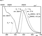
In
In
Es sei besonders herausgestellt, dass die für diese Verbindung gemessene Emissionsquantenausbeute mit ϕPL(300 K) = 92% außerordentlich hoch ist.It should be emphasized that the emission quantum yield measured for this compound is extraordinarily high with φ PL (300 K) = 92%.
In den
bAnregungswellenlänge λexc = 400 nm
cDie Abklingkurve weicht vom monoexponentiellen Verhalten ab. Die Abklingzeit wurde durch eine biexpo nentielle Ausgleichkurve bestimmt.
dLange KomponenteIn the
b excitation wavelength λ exc = 400 nm
c The decay curve deviates from mono-exponential behavior. The cooldown was determined by a biexpo nentielle compensation curve.
d Long component
Figurencharacters
ZITATE ENTHALTEN IN DER BESCHREIBUNG QUOTES INCLUDE IN THE DESCRIPTION
Diese Liste der vom Anmelder aufgeführten Dokumente wurde automatisiert erzeugt und ist ausschließlich zur besseren Information des Lesers aufgenommen. Die Liste ist nicht Bestandteil der deutschen Patent- bzw. Gebrauchsmusteranmeldung. Das DPMA übernimmt keinerlei Haftung für etwaige Fehler oder Auslassungen.This list of the documents listed by the applicant has been generated automatically and is included solely for the better information of the reader. The list is not part of the German patent or utility model application. The DPMA assumes no liability for any errors or omissions.
Zitierte Nicht-PatentliteraturCited non-patent literature
- H. Yersin, Top. Curr. Chem. 2004, 241, 1 [0005] H. Yersin, Top. Curr. Chem. 2004, 241, 1 [0005]
- Yersin, „Highly Efficient OLEDs with Phosphorescent Materials”; Wiley-VCH, Weinheim, Germany, 2008 [0005] Yersin, "Highly Efficient OLEDs with Phosphorescent Materials"; Wiley-VCH, Weinheim, Germany, 2008 [0005]
- Tang et al., Appl. Phys. Lett. 1987, 51, 913 [0006] Tang et al., Appl. Phys. Lett. 1987, 51, 913 [0006]
- H. Yersin, Top. Curr. Chem. 2004, 241, 1 [0009] H. Yersin, Top. Curr. Chem. 2004, 241, 1 [0009]
- M. A. Baldo, D. F. O'Brien, M. E. Thompson, S. R. Forrest, Phys. Rev. B 1999, 60, 14422 [0009] MA Baldo, DF O'Brien, ME Thompson, SR Forrest, Phys. Rev. B 1999, 60, 14422 [0009]
- S. L. Murov, J. Carmicheal, G. L. Hug, Handbook of Photochemistry, 2nd Edition, Marcel Dekker, New York 1993, S. 338 ff [0009] SL Murov, J. Carmicheal, GL Hug, Handbook of Photochemistry, 2nd Edition, Marcel Dekker, New York 1993, p. 338 et seq. [0009]
- S. L. Murov, J. Carmicheal, G. L. Hug, Handbook of Photochemistry, 2nd Edition, Marcel Dekker, New York 1993, S. 338 ff [0010] SL Murov, J. Carmicheal, GL Hug, Handbook of Photochemistry, 2nd Edition, Marcel Dekker, New York 1993, p. 338 et seq. [0010]
- H. Yersin, „Highly Efficient OLEDs with Phosphorescent Materials”, Wiley-VCH, Weinheim 2008 [0010] H. Yersin, "Highly Efficient OLEDs with Phosphorescent Materials", Wiley-VCH, Weinheim 2008. [0010]
-
S. R. Forrest et al., Phys. Rev. B 2008, 77, 235215 [0010] SR Forrest et al.,
Phys. Rev. B 2008, 77, 235215 [0010] - J. Kido et al. Jap. J. Appl. Phys. 2007, 46, L10 [0010] J. Kido et al. Jap. J. Appl. Phys. 2007, 46, L10 [0010]
Claims (13)


Priority Applications (8)
| Application Number | Priority Date | Filing Date | Title |
|---|---|---|---|
| DE102011080240A DE102011080240A1 (en) | 2011-08-02 | 2011-08-02 | Singlet Harvesting with binuclear copper (I) complexes for opto-electronic devices |
| EP12162191A EP2554625A1 (en) | 2011-08-02 | 2012-03-29 | Singlet harvesting with two-core copper(I) complexes for opto-electronic devices |
| CN201280037853.1A CN103748191B (en) | 2011-08-02 | 2012-08-02 | It is a kind of that there is double-core copper for optoelectronic device(I)The singlet state capture of complex |
| PCT/EP2012/065203 WO2013017675A1 (en) | 2011-08-02 | 2012-08-02 | Singlet harvesting with dual-core copper (i) complexes for optoelectronic devices |
| KR1020147004338A KR20140068027A (en) | 2011-08-02 | 2012-08-02 | Singlet harvesting with dual-core copper (i) complexes for optoelectronic devices |
| EP12753670.4A EP2739702B1 (en) | 2011-08-02 | 2012-08-02 | Singlet harvesting with two-core copper(i) complexes for opto-electronic devices |
| JP2014523336A JP2014532034A (en) | 2011-08-02 | 2012-08-02 | Singlet harvesting with dual-core copper (I) complexes for optoelectronic devices |
| US14/236,202 US9537117B2 (en) | 2011-08-02 | 2012-08-02 | Singlet harvesting with dual-core copper (I) complexes for optoelectronic devices |
Applications Claiming Priority (1)
| Application Number | Priority Date | Filing Date | Title |
|---|---|---|---|
| DE102011080240A DE102011080240A1 (en) | 2011-08-02 | 2011-08-02 | Singlet Harvesting with binuclear copper (I) complexes for opto-electronic devices |
Publications (1)
| Publication Number | Publication Date |
|---|---|
| DE102011080240A1 true DE102011080240A1 (en) | 2013-02-07 |
Family
ID=45928721
Family Applications (1)
| Application Number | Title | Priority Date | Filing Date |
|---|---|---|---|
| DE102011080240A Withdrawn DE102011080240A1 (en) | 2011-08-02 | 2011-08-02 | Singlet Harvesting with binuclear copper (I) complexes for opto-electronic devices |
Country Status (7)
| Country | Link |
|---|---|
| US (1) | US9537117B2 (en) |
| EP (2) | EP2554625A1 (en) |
| JP (1) | JP2014532034A (en) |
| KR (1) | KR20140068027A (en) |
| CN (1) | CN103748191B (en) |
| DE (1) | DE102011080240A1 (en) |
| WO (1) | WO2013017675A1 (en) |
Cited By (2)
| Publication number | Priority date | Publication date | Assignee | Title |
|---|---|---|---|---|
| DE102013111552A1 (en) * | 2013-10-21 | 2015-04-23 | Osram Oled Gmbh | Organic light emitting device |
| DE102014111276B4 (en) | 2014-08-07 | 2021-09-02 | Pictiva Displays International Limited | Process for the production of organic functional layers and for the production of an organic electronic component |
Families Citing this family (34)
| Publication number | Priority date | Publication date | Assignee | Title |
|---|---|---|---|---|
| EP2707374B1 (en) | 2011-05-13 | 2016-03-02 | cynora GmbH | Copper(i)complexes, in particular for optoelectronic devices |
| DE102011089687A1 (en) * | 2011-12-22 | 2013-06-27 | Hartmut Yersin | Singlet Harvesting with special organic molecules without metal centers for opto-electronic devices |
| WO2014201377A1 (en) * | 2013-06-14 | 2014-12-18 | Rutgers, The State University Of New Jersey | Light emitting hybrid semiconductors based on ib-vii binary compounds |
| KR102054342B1 (en) | 2013-08-26 | 2019-12-11 | 가부시키가이샤 한도오따이 에네루기 켄큐쇼 | Light-emitting element, light-emitting device, display device, lighting device, and electronic appliance |
| CN105993083B (en) | 2013-12-20 | 2018-07-03 | Udc 爱尔兰有限责任公司 | Efficient OLED device with extremely short decay time |
| TWI729649B (en) | 2014-05-30 | 2021-06-01 | 日商半導體能源研究所股份有限公司 | Light-emitting element, light-emitting device, electronic device, and lighting device |
| WO2016034556A2 (en) * | 2014-09-02 | 2016-03-10 | Cynora Gmbh | Opto-electronic device containing emitter compound with high quantum yield and solubility |
| EP2993176A1 (en) | 2014-09-02 | 2016-03-09 | cynora GmbH | Metal (i) complexes for improved conductivity |
| DE102015216658A1 (en) | 2014-09-02 | 2016-03-03 | Cynora Gmbh | Structurally stabilized copper (I) complexes |
| WO2016037963A1 (en) | 2014-09-08 | 2016-03-17 | Cynora Gmbh | Stabilized optically active layer and method for production |
| WO2016037964A1 (en) | 2014-09-08 | 2016-03-17 | Cynora Gmbh | Improved optically active layer and method for the production thereof |
| KR102460646B1 (en) | 2014-09-16 | 2022-10-31 | 삼성디스플레이 주식회사 | Light―emitting layer suitable for bright luminescence |
| WO2016079097A1 (en) | 2014-11-18 | 2016-05-26 | Cynora Gmbh | Copper(i) complexes for optoelectronic applications |
| US10903440B2 (en) | 2015-02-24 | 2021-01-26 | Semiconductor Energy Laboratory Co., Ltd. | Light-emitting element, light-emitting device, electronic device, and lighting device |
| KR102661925B1 (en) | 2015-06-03 | 2024-05-02 | 유디씨 아일랜드 리미티드 | Highly efficient oled devices with very short decay times |
| CN104877673B (en) * | 2015-06-23 | 2016-11-30 | 江西理工大学 | Pyridine pyrazoles double-core copper [I] complex luminescent material and preparation method |
| CN107793438B (en) * | 2017-08-29 | 2019-11-12 | 中山大学 | A kind of copper (I) phosphine benzene heterocycle complex and its preparation method and application |
| CN112514092A (en) | 2018-07-23 | 2021-03-16 | 三星显示有限公司 | Organic light emitting device |
| KR20210057092A (en) | 2018-09-12 | 2021-05-20 | 메르크 파텐트 게엠베하 | Materials for organic electroluminescent devices |
| TWI826522B (en) | 2018-09-12 | 2023-12-21 | 德商麥克專利有限公司 | Electroluminescent devices |
| TW202030902A (en) | 2018-09-12 | 2020-08-16 | 德商麥克專利有限公司 | Electroluminescent devices |
| KR102661468B1 (en) | 2019-02-15 | 2024-04-30 | 삼성디스플레이 주식회사 | Organic light emitting device and electronic apparatus comprising the same |
| US20220127286A1 (en) | 2019-03-04 | 2022-04-28 | Merck Patent Gmbh | Ligands for nano-sized materials |
| US11462692B2 (en) * | 2019-03-21 | 2022-10-04 | Samsung Display Co., Ltd. | Organic electroluminescent device |
| EP3935063A1 (en) | 2019-04-11 | 2022-01-12 | Merck Patent GmbH | Materials for organic electroluminescent devices |
| EP4055642A1 (en) | 2019-11-04 | 2022-09-14 | Merck Patent GmbH | Materials for organic electroluminescent devices |
| TW202134252A (en) | 2019-11-12 | 2021-09-16 | 德商麥克專利有限公司 | Materials for organic electroluminescent devices |
| KR20210059153A (en) | 2019-11-14 | 2021-05-25 | 삼성디스플레이 주식회사 | Organic light emitting device and apparatus comprising the same |
| TW202136181A (en) | 2019-12-04 | 2021-10-01 | 德商麥克專利有限公司 | Materials for organic electroluminescent devices |
| WO2021151922A1 (en) | 2020-01-29 | 2021-08-05 | Merck Patent Gmbh | Benzimidazole derivatives |
| US20230337537A1 (en) | 2020-03-23 | 2023-10-19 | Merck Patent Gmbh | Materials for organic electroluminescent devices |
| KR20210136224A (en) | 2020-05-06 | 2021-11-17 | 삼성디스플레이 주식회사 | Llight emitting device and electronic apparatus comprising same |
| CN112961171B (en) * | 2021-02-08 | 2023-10-03 | 浙江理工大学 | Application of binuclear cuprous complex sensing material in fluorescence sensing of nitrogenous heterocyclic VOCs |
| WO2024105066A1 (en) | 2022-11-17 | 2024-05-23 | Merck Patent Gmbh | Materials for organic electroluminescent devices |
Family Cites Families (9)
| Publication number | Priority date | Publication date | Assignee | Title |
|---|---|---|---|---|
| JP4328702B2 (en) * | 2003-12-01 | 2009-09-09 | キヤノン株式会社 | Organic EL device |
| DE102004010954A1 (en) * | 2004-03-03 | 2005-10-06 | Novaled Gmbh | Use of a metal complex as an n-dopant for an organic semiconductive matrix material, organic semiconductor material and electronic component |
| US7462406B2 (en) * | 2005-11-15 | 2008-12-09 | Eastman Kodak Company | OLED devices with dinuclear copper compounds |
| GB2440367A (en) * | 2006-07-26 | 2008-01-30 | Oled T Ltd | Electroluminescent device |
| US7683183B2 (en) * | 2006-07-28 | 2010-03-23 | California Institute Of Technology | Emissive monomeric metal complexes |
| DE102008033563A1 (en) * | 2008-07-17 | 2010-01-21 | Merck Patent Gmbh | Complexes with Small Singlet-Triplet Energy Intervals for Use in Opto-Electronic Devices (Singlet Harvesting Effect) |
| DE102009030475A1 (en) * | 2009-06-24 | 2011-01-05 | Hartmut Prof. Dr. Yersin | Copper complexes for optoelectronic applications |
| US8580394B2 (en) * | 2009-11-19 | 2013-11-12 | Universal Display Corporation | 3-coordinate copper(I)-carbene complexes |
| EP2707374B1 (en) * | 2011-05-13 | 2016-03-02 | cynora GmbH | Copper(i)complexes, in particular for optoelectronic devices |
-
2011
- 2011-08-02 DE DE102011080240A patent/DE102011080240A1/en not_active Withdrawn
-
2012
- 2012-03-29 EP EP12162191A patent/EP2554625A1/en not_active Withdrawn
- 2012-08-02 US US14/236,202 patent/US9537117B2/en active Active
- 2012-08-02 JP JP2014523336A patent/JP2014532034A/en active Pending
- 2012-08-02 WO PCT/EP2012/065203 patent/WO2013017675A1/en active Application Filing
- 2012-08-02 CN CN201280037853.1A patent/CN103748191B/en active Active
- 2012-08-02 EP EP12753670.4A patent/EP2739702B1/en active Active
- 2012-08-02 KR KR1020147004338A patent/KR20140068027A/en not_active Application Discontinuation
Non-Patent Citations (8)
| Title |
|---|
| H. Yersin, "Highly Efficient OLEDs with Phosphorescent Materials", Wiley-VCH, Weinheim 2008 |
| H. Yersin, Top. Curr. Chem. 2004, 241, 1 |
| J. Kido et al. Jap. J. Appl. Phys. 2007, 46, L10 |
| M. A. Baldo, D. F. O'Brien, M. E. Thompson, S. R. Forrest, Phys. Rev. B 1999, 60, 14422 |
| S. L. Murov, J. Carmicheal, G. L. Hug, Handbook of Photochemistry, 2nd Edition, Marcel Dekker, New York 1993, S. 338 ff |
| S. R. Forrest et al., Phys. Rev. B 2008, 77, 235215 |
| Tang et al., Appl. Phys. Lett. 1987, 51, 913 |
| Yersin, "Highly Efficient OLEDs with Phosphorescent Materials"; Wiley-VCH, Weinheim, Germany, 2008 |
Cited By (2)
| Publication number | Priority date | Publication date | Assignee | Title |
|---|---|---|---|---|
| DE102013111552A1 (en) * | 2013-10-21 | 2015-04-23 | Osram Oled Gmbh | Organic light emitting device |
| DE102014111276B4 (en) | 2014-08-07 | 2021-09-02 | Pictiva Displays International Limited | Process for the production of organic functional layers and for the production of an organic electronic component |
Also Published As
| Publication number | Publication date |
|---|---|
| WO2013017675A1 (en) | 2013-02-07 |
| US9537117B2 (en) | 2017-01-03 |
| JP2014532034A (en) | 2014-12-04 |
| US20140167027A1 (en) | 2014-06-19 |
| EP2739702B1 (en) | 2016-03-30 |
| KR20140068027A (en) | 2014-06-05 |
| CN103748191B (en) | 2017-12-08 |
| EP2554625A1 (en) | 2013-02-06 |
| CN103748191A (en) | 2014-04-23 |
| EP2739702A1 (en) | 2014-06-11 |
Similar Documents
| Publication | Publication Date | Title |
|---|---|---|
| EP2739702B1 (en) | Singlet harvesting with two-core copper(i) complexes for opto-electronic devices | |
| EP2588563B1 (en) | Singlet harvesting with organic molecules for optoelectronic devices | |
| EP2595997B1 (en) | Copper(i) complexes for optoelectronic devices | |
| EP2712000B1 (en) | Materials for Organic Electroluminescent Devices | |
| DE102009030475A1 (en) | Copper complexes for optoelectronic applications | |
| EP2795691B1 (en) | Organic molecules for oleds and other optoelectronic devices | |
| EP2340577B1 (en) | Organic electroluminescent device | |
| EP2666195A1 (en) | Metal complexes having variable emission colours for optoelectronic devices | |
| WO2008043562A1 (en) | Lanthanoid emitter for oled applications | |
| EP2933850A1 (en) | Metal complexes as emitter materials | |
| DE102013100181A1 (en) | Thermally activated fluorescence and singlet harvesting with rigid metal complexes for opto-electronic devices | |
| WO2014202675A1 (en) | Extended singlet harvesting for oleds and other optoelectronic devices | |
| EP3221422B1 (en) | Copper(i) complexes for optoelectronic applications | |
| DE112009001538T5 (en) | Composition and produced using the composition light emitting element | |
| DE102016115633A1 (en) | Silver complexes with nido-carborane ligands with thermally-activated delayed fluorescence for opto-electronic devices | |
| DE102011104169A1 (en) | Radiation-emitting component and method for producing a radiation-emitting component | |
| WO2023079035A1 (en) | Emitter material for oleds | |
| DE102015108002A1 (en) | Composition for use in optoelectronic devices | |
| DE102014116314A1 (en) | Triplex ligand metal complex compounds for improved singlet harvesting by combined singlet and triplet emission for OLEDs and other optoelectronic devices | |
| DE102011000282A1 (en) | Shifting the emission wavelength of a metal complex emitting in a given wavelength, to a wavelength which is greater than the given wavelength, useful in e.g. organic diodes, comprises embedding the metal complex into a polymer matrix | |
| DE102007061755A1 (en) | Component for phosphorescent light emission from triplet states and method for producing such devices |
Legal Events
| Date | Code | Title | Description |
|---|---|---|---|
| R082 | Change of representative |
Representative=s name: HOPPE, GEORG JOHANNES, DIPL.-BIOCHEM. DR. RER., DE |
|
| R119 | Application deemed withdrawn, or ip right lapsed, due to non-payment of renewal fee |