DE102004044149B4 - High-performance light emitting diode device - Google Patents
High-performance light emitting diode device Download PDFInfo
- Publication number
- DE102004044149B4 DE102004044149B4 DE102004044149A DE102004044149A DE102004044149B4 DE 102004044149 B4 DE102004044149 B4 DE 102004044149B4 DE 102004044149 A DE102004044149 A DE 102004044149A DE 102004044149 A DE102004044149 A DE 102004044149A DE 102004044149 B4 DE102004044149 B4 DE 102004044149B4
- Authority
- DE
- Germany
- Prior art keywords
- circuit element
- heat
- element according
- chip
- circuit
- Prior art date
- Legal status (The legal status is an assumption and is not a legal conclusion. Google has not performed a legal analysis and makes no representation as to the accuracy of the status listed.)
- Expired - Fee Related
Links
- 239000004020 conductor Substances 0.000 claims abstract description 12
- 229910000679 solder Inorganic materials 0.000 claims description 26
- 239000000758 substrate Substances 0.000 claims description 26
- 239000000463 material Substances 0.000 claims description 13
- 238000005538 encapsulation Methods 0.000 claims description 12
- RYGMFSIKBFXOCR-UHFFFAOYSA-N Copper Chemical compound [Cu] RYGMFSIKBFXOCR-UHFFFAOYSA-N 0.000 claims description 7
- 229910052802 copper Inorganic materials 0.000 claims description 6
- 239000010949 copper Substances 0.000 claims description 6
- 229910052782 aluminium Inorganic materials 0.000 claims description 4
- XAGFODPZIPBFFR-UHFFFAOYSA-N aluminium Chemical group [Al] XAGFODPZIPBFFR-UHFFFAOYSA-N 0.000 claims description 4
- 239000000853 adhesive Substances 0.000 description 11
- 230000001070 adhesive effect Effects 0.000 description 11
- 239000010410 layer Substances 0.000 description 11
- 229910052751 metal Inorganic materials 0.000 description 8
- 239000002184 metal Substances 0.000 description 8
- 230000017525 heat dissipation Effects 0.000 description 6
- 239000004065 semiconductor Substances 0.000 description 5
- 238000000034 method Methods 0.000 description 4
- 239000010409 thin film Substances 0.000 description 4
- GGMPTLAAIUQMIE-UHFFFAOYSA-N 2,3,4,5,6-pentachlorobiphenyl Chemical compound ClC1=C(Cl)C(Cl)=C(Cl)C(Cl)=C1C1=CC=CC=C1 GGMPTLAAIUQMIE-UHFFFAOYSA-N 0.000 description 3
- 239000002131 composite material Substances 0.000 description 3
- 238000010276 construction Methods 0.000 description 3
- 239000008393 encapsulating agent Substances 0.000 description 3
- 150000003071 polychlorinated biphenyls Chemical class 0.000 description 3
- 239000004593 Epoxy Substances 0.000 description 2
- 239000012790 adhesive layer Substances 0.000 description 2
- 150000001875 compounds Chemical class 0.000 description 2
- 239000011521 glass Substances 0.000 description 2
- 230000007246 mechanism Effects 0.000 description 2
- 238000000465 moulding Methods 0.000 description 2
- 230000008569 process Effects 0.000 description 2
- 239000011347 resin Substances 0.000 description 2
- 229920005989 resin Polymers 0.000 description 2
- 238000009423 ventilation Methods 0.000 description 2
- 229910002601 GaN Inorganic materials 0.000 description 1
- 229910005540 GaP Inorganic materials 0.000 description 1
- JMASRVWKEDWRBT-UHFFFAOYSA-N Gallium nitride Chemical compound [Ga]#N JMASRVWKEDWRBT-UHFFFAOYSA-N 0.000 description 1
- AJGDITRVXRPLBY-UHFFFAOYSA-N aluminum indium Chemical compound [Al].[In] AJGDITRVXRPLBY-UHFFFAOYSA-N 0.000 description 1
- 239000000872 buffer Substances 0.000 description 1
- 239000000919 ceramic Substances 0.000 description 1
- 239000011889 copper foil Substances 0.000 description 1
- 230000008878 coupling Effects 0.000 description 1
- 238000010168 coupling process Methods 0.000 description 1
- 238000005859 coupling reaction Methods 0.000 description 1
- 230000007423 decrease Effects 0.000 description 1
- 238000000605 extraction Methods 0.000 description 1
- HZXMRANICFIONG-UHFFFAOYSA-N gallium phosphide Chemical compound [Ga]#P HZXMRANICFIONG-UHFFFAOYSA-N 0.000 description 1
- 229910052738 indium Inorganic materials 0.000 description 1
- APFVFJFRJDLVQX-UHFFFAOYSA-N indium atom Chemical compound [In] APFVFJFRJDLVQX-UHFFFAOYSA-N 0.000 description 1
- 238000004519 manufacturing process Methods 0.000 description 1
- 229920000642 polymer Polymers 0.000 description 1
- 229920001296 polysiloxane Polymers 0.000 description 1
- 238000010248 power generation Methods 0.000 description 1
- 230000002035 prolonged effect Effects 0.000 description 1
Images


Classifications
-
- H—ELECTRICITY
- H01—ELECTRIC ELEMENTS
- H01L—SEMICONDUCTOR DEVICES NOT COVERED BY CLASS H10
- H01L33/00—Semiconductor devices having potential barriers specially adapted for light emission; Processes or apparatus specially adapted for the manufacture or treatment thereof or of parts thereof; Details thereof
- H01L33/48—Semiconductor devices having potential barriers specially adapted for light emission; Processes or apparatus specially adapted for the manufacture or treatment thereof or of parts thereof; Details thereof characterised by the semiconductor body packages
- H01L33/62—Arrangements for conducting electric current to or from the semiconductor body, e.g. lead-frames, wire-bonds or solder balls
-
- H—ELECTRICITY
- H01—ELECTRIC ELEMENTS
- H01L—SEMICONDUCTOR DEVICES NOT COVERED BY CLASS H10
- H01L23/00—Details of semiconductor or other solid state devices
- H01L23/34—Arrangements for cooling, heating, ventilating or temperature compensation ; Temperature sensing arrangements
-
- H—ELECTRICITY
- H01—ELECTRIC ELEMENTS
- H01L—SEMICONDUCTOR DEVICES NOT COVERED BY CLASS H10
- H01L23/00—Details of semiconductor or other solid state devices
- H01L23/34—Arrangements for cooling, heating, ventilating or temperature compensation ; Temperature sensing arrangements
- H01L23/36—Selection of materials, or shaping, to facilitate cooling or heating, e.g. heatsinks
-
- H—ELECTRICITY
- H01—ELECTRIC ELEMENTS
- H01L—SEMICONDUCTOR DEVICES NOT COVERED BY CLASS H10
- H01L23/00—Details of semiconductor or other solid state devices
- H01L23/48—Arrangements for conducting electric current to or from the solid state body in operation, e.g. leads, terminal arrangements ; Selection of materials therefor
-
- H—ELECTRICITY
- H01—ELECTRIC ELEMENTS
- H01L—SEMICONDUCTOR DEVICES NOT COVERED BY CLASS H10
- H01L33/00—Semiconductor devices having potential barriers specially adapted for light emission; Processes or apparatus specially adapted for the manufacture or treatment thereof or of parts thereof; Details thereof
- H01L33/48—Semiconductor devices having potential barriers specially adapted for light emission; Processes or apparatus specially adapted for the manufacture or treatment thereof or of parts thereof; Details thereof characterised by the semiconductor body packages
- H01L33/64—Heat extraction or cooling elements
-
- H—ELECTRICITY
- H01—ELECTRIC ELEMENTS
- H01L—SEMICONDUCTOR DEVICES NOT COVERED BY CLASS H10
- H01L2224/00—Indexing scheme for arrangements for connecting or disconnecting semiconductor or solid-state bodies and methods related thereto as covered by H01L24/00
- H01L2224/01—Means for bonding being attached to, or being formed on, the surface to be connected, e.g. chip-to-package, die-attach, "first-level" interconnects; Manufacturing methods related thereto
- H01L2224/26—Layer connectors, e.g. plate connectors, solder or adhesive layers; Manufacturing methods related thereto
- H01L2224/31—Structure, shape, material or disposition of the layer connectors after the connecting process
- H01L2224/32—Structure, shape, material or disposition of the layer connectors after the connecting process of an individual layer connector
- H01L2224/321—Disposition
- H01L2224/32151—Disposition the layer connector connecting between a semiconductor or solid-state body and an item not being a semiconductor or solid-state body, e.g. chip-to-substrate, chip-to-passive
- H01L2224/32221—Disposition the layer connector connecting between a semiconductor or solid-state body and an item not being a semiconductor or solid-state body, e.g. chip-to-substrate, chip-to-passive the body and the item being stacked
- H01L2224/32245—Disposition the layer connector connecting between a semiconductor or solid-state body and an item not being a semiconductor or solid-state body, e.g. chip-to-substrate, chip-to-passive the body and the item being stacked the item being metallic
- H01L2224/32257—Disposition the layer connector connecting between a semiconductor or solid-state body and an item not being a semiconductor or solid-state body, e.g. chip-to-substrate, chip-to-passive the body and the item being stacked the item being metallic the layer connector connecting to a bonding area disposed in a recess of the surface of the item
-
- H—ELECTRICITY
- H01—ELECTRIC ELEMENTS
- H01L—SEMICONDUCTOR DEVICES NOT COVERED BY CLASS H10
- H01L2224/00—Indexing scheme for arrangements for connecting or disconnecting semiconductor or solid-state bodies and methods related thereto as covered by H01L24/00
- H01L2224/01—Means for bonding being attached to, or being formed on, the surface to be connected, e.g. chip-to-package, die-attach, "first-level" interconnects; Manufacturing methods related thereto
- H01L2224/42—Wire connectors; Manufacturing methods related thereto
- H01L2224/47—Structure, shape, material or disposition of the wire connectors after the connecting process
- H01L2224/48—Structure, shape, material or disposition of the wire connectors after the connecting process of an individual wire connector
- H01L2224/4805—Shape
- H01L2224/4809—Loop shape
- H01L2224/48091—Arched
-
- H—ELECTRICITY
- H01—ELECTRIC ELEMENTS
- H01L—SEMICONDUCTOR DEVICES NOT COVERED BY CLASS H10
- H01L2224/00—Indexing scheme for arrangements for connecting or disconnecting semiconductor or solid-state bodies and methods related thereto as covered by H01L24/00
- H01L2224/01—Means for bonding being attached to, or being formed on, the surface to be connected, e.g. chip-to-package, die-attach, "first-level" interconnects; Manufacturing methods related thereto
- H01L2224/42—Wire connectors; Manufacturing methods related thereto
- H01L2224/47—Structure, shape, material or disposition of the wire connectors after the connecting process
- H01L2224/48—Structure, shape, material or disposition of the wire connectors after the connecting process of an individual wire connector
- H01L2224/481—Disposition
- H01L2224/48151—Connecting between a semiconductor or solid-state body and an item not being a semiconductor or solid-state body, e.g. chip-to-substrate, chip-to-passive
- H01L2224/48221—Connecting between a semiconductor or solid-state body and an item not being a semiconductor or solid-state body, e.g. chip-to-substrate, chip-to-passive the body and the item being stacked
- H01L2224/48245—Connecting between a semiconductor or solid-state body and an item not being a semiconductor or solid-state body, e.g. chip-to-substrate, chip-to-passive the body and the item being stacked the item being metallic
- H01L2224/48247—Connecting between a semiconductor or solid-state body and an item not being a semiconductor or solid-state body, e.g. chip-to-substrate, chip-to-passive the body and the item being stacked the item being metallic connecting the wire to a bond pad of the item
-
- H—ELECTRICITY
- H01—ELECTRIC ELEMENTS
- H01L—SEMICONDUCTOR DEVICES NOT COVERED BY CLASS H10
- H01L2224/00—Indexing scheme for arrangements for connecting or disconnecting semiconductor or solid-state bodies and methods related thereto as covered by H01L24/00
- H01L2224/01—Means for bonding being attached to, or being formed on, the surface to be connected, e.g. chip-to-package, die-attach, "first-level" interconnects; Manufacturing methods related thereto
- H01L2224/42—Wire connectors; Manufacturing methods related thereto
- H01L2224/47—Structure, shape, material or disposition of the wire connectors after the connecting process
- H01L2224/49—Structure, shape, material or disposition of the wire connectors after the connecting process of a plurality of wire connectors
- H01L2224/491—Disposition
- H01L2224/4912—Layout
- H01L2224/49175—Parallel arrangements
-
- H—ELECTRICITY
- H01—ELECTRIC ELEMENTS
- H01L—SEMICONDUCTOR DEVICES NOT COVERED BY CLASS H10
- H01L2224/00—Indexing scheme for arrangements for connecting or disconnecting semiconductor or solid-state bodies and methods related thereto as covered by H01L24/00
- H01L2224/73—Means for bonding being of different types provided for in two or more of groups H01L2224/10, H01L2224/18, H01L2224/26, H01L2224/34, H01L2224/42, H01L2224/50, H01L2224/63, H01L2224/71
- H01L2224/732—Location after the connecting process
- H01L2224/73251—Location after the connecting process on different surfaces
- H01L2224/73265—Layer and wire connectors
-
- H—ELECTRICITY
- H01—ELECTRIC ELEMENTS
- H01L—SEMICONDUCTOR DEVICES NOT COVERED BY CLASS H10
- H01L24/00—Arrangements for connecting or disconnecting semiconductor or solid-state bodies; Methods or apparatus related thereto
- H01L24/01—Means for bonding being attached to, or being formed on, the surface to be connected, e.g. chip-to-package, die-attach, "first-level" interconnects; Manufacturing methods related thereto
- H01L24/42—Wire connectors; Manufacturing methods related thereto
- H01L24/47—Structure, shape, material or disposition of the wire connectors after the connecting process
- H01L24/48—Structure, shape, material or disposition of the wire connectors after the connecting process of an individual wire connector
-
- H—ELECTRICITY
- H01—ELECTRIC ELEMENTS
- H01L—SEMICONDUCTOR DEVICES NOT COVERED BY CLASS H10
- H01L24/00—Arrangements for connecting or disconnecting semiconductor or solid-state bodies; Methods or apparatus related thereto
- H01L24/01—Means for bonding being attached to, or being formed on, the surface to be connected, e.g. chip-to-package, die-attach, "first-level" interconnects; Manufacturing methods related thereto
- H01L24/42—Wire connectors; Manufacturing methods related thereto
- H01L24/47—Structure, shape, material or disposition of the wire connectors after the connecting process
- H01L24/49—Structure, shape, material or disposition of the wire connectors after the connecting process of a plurality of wire connectors
-
- H—ELECTRICITY
- H01—ELECTRIC ELEMENTS
- H01L—SEMICONDUCTOR DEVICES NOT COVERED BY CLASS H10
- H01L2924/00—Indexing scheme for arrangements or methods for connecting or disconnecting semiconductor or solid-state bodies as covered by H01L24/00
- H01L2924/0001—Technical content checked by a classifier
- H01L2924/00014—Technical content checked by a classifier the subject-matter covered by the group, the symbol of which is combined with the symbol of this group, being disclosed without further technical details
-
- H—ELECTRICITY
- H01—ELECTRIC ELEMENTS
- H01L—SEMICONDUCTOR DEVICES NOT COVERED BY CLASS H10
- H01L2924/00—Indexing scheme for arrangements or methods for connecting or disconnecting semiconductor or solid-state bodies as covered by H01L24/00
- H01L2924/01—Chemical elements
- H01L2924/01068—Erbium [Er]
-
- H—ELECTRICITY
- H01—ELECTRIC ELEMENTS
- H01L—SEMICONDUCTOR DEVICES NOT COVERED BY CLASS H10
- H01L2924/00—Indexing scheme for arrangements or methods for connecting or disconnecting semiconductor or solid-state bodies as covered by H01L24/00
- H01L2924/10—Details of semiconductor or other solid state devices to be connected
- H01L2924/11—Device type
- H01L2924/12—Passive devices, e.g. 2 terminal devices
- H01L2924/1204—Optical Diode
- H01L2924/12041—LED
-
- H—ELECTRICITY
- H01—ELECTRIC ELEMENTS
- H01L—SEMICONDUCTOR DEVICES NOT COVERED BY CLASS H10
- H01L2924/00—Indexing scheme for arrangements or methods for connecting or disconnecting semiconductor or solid-state bodies as covered by H01L24/00
- H01L2924/10—Details of semiconductor or other solid state devices to be connected
- H01L2924/11—Device type
- H01L2924/14—Integrated circuits
-
- H—ELECTRICITY
- H01—ELECTRIC ELEMENTS
- H01L—SEMICONDUCTOR DEVICES NOT COVERED BY CLASS H10
- H01L2924/00—Indexing scheme for arrangements or methods for connecting or disconnecting semiconductor or solid-state bodies as covered by H01L24/00
- H01L2924/15—Details of package parts other than the semiconductor or other solid state devices to be connected
- H01L2924/151—Die mounting substrate
- H01L2924/153—Connection portion
- H01L2924/1531—Connection portion the connection portion being formed only on the surface of the substrate opposite to the die mounting surface
- H01L2924/15311—Connection portion the connection portion being formed only on the surface of the substrate opposite to the die mounting surface being a ball array, e.g. BGA
-
- H—ELECTRICITY
- H01—ELECTRIC ELEMENTS
- H01L—SEMICONDUCTOR DEVICES NOT COVERED BY CLASS H10
- H01L2924/00—Indexing scheme for arrangements or methods for connecting or disconnecting semiconductor or solid-state bodies as covered by H01L24/00
- H01L2924/15—Details of package parts other than the semiconductor or other solid state devices to be connected
- H01L2924/151—Die mounting substrate
- H01L2924/153—Connection portion
- H01L2924/1532—Connection portion the connection portion being formed on the die mounting surface of the substrate
-
- H—ELECTRICITY
- H01—ELECTRIC ELEMENTS
- H01L—SEMICONDUCTOR DEVICES NOT COVERED BY CLASS H10
- H01L2924/00—Indexing scheme for arrangements or methods for connecting or disconnecting semiconductor or solid-state bodies as covered by H01L24/00
- H01L2924/15—Details of package parts other than the semiconductor or other solid state devices to be connected
- H01L2924/181—Encapsulation
- H01L2924/1815—Shape
Landscapes
- Engineering & Computer Science (AREA)
- Microelectronics & Electronic Packaging (AREA)
- Computer Hardware Design (AREA)
- Power Engineering (AREA)
- Physics & Mathematics (AREA)
- Condensed Matter Physics & Semiconductors (AREA)
- General Physics & Mathematics (AREA)
- Manufacturing & Machinery (AREA)
- Chemical & Material Sciences (AREA)
- Materials Engineering (AREA)
- Led Device Packages (AREA)
Abstract
Schaltungselement (300; 400; 600; 700) mit folgenden Merkmalen:
einem wärmeleitenden Körper (301; 401; 601; 701), der eine obere (302; 402; 602; 702) und eine untere (304; 404; 604; 704) Oberfläche aufweist, wobei die untere Oberfläche des wärmeleitenden Körpers eine Oberfläche aufweist, die eine größere Oberflächenfläche aufweist als die obere Oberfläche des wärmeleitenden Körpers;
einem Chip, auf dem sich eine elektronische Schaltung befindet, wobei der Chip einen ersten und einen zweiten Kontaktpunkt zur Leistungsversorgung der elektronischen Schaltung umfasst, wobei der Chip in thermischem Kontakt mit dem wärmeleitenden Körper steht, und wobei der Chip eine untere Oberfläche aufweist, die kleiner ist als die obere Oberfläche des wärmeleitenden Körpers;
einer ersten Leiterbahn (306, 308), die ein elektrisch leitendes Material aufweist, das an der oberen Oberfläche (302; 402; 602; 702) des wärmeleitenden Körpers angebracht ist und elektrisch von demselben isoliert ist;
einem ersten elektrisch leitenden (318, 320) Pfad von dem...Circuit element (300; 400; 600; 700) having the following features:
a heat conductive body (301; 401; 601; 701) having an upper (302; 402; 602; 702) and a lower (304; 404; 604; 704) surface, the lower surface of the heat conductive body having a surface having a larger surface area than the upper surface of the heat conductive body;
a chip having an electronic circuit thereon, the chip including first and second points of contact for powering the electronic circuit, the chip being in thermal contact with the heat conductive body, and the chip having a bottom surface that is smaller is as the upper surface of the heat conductive body;
a first conductive trace (306, 308) comprising an electrically conductive material attached to and electrically isolated from the upper surface (302; 402; 602; 702) of the thermally conductive body;
a first electrically conductive (318, 320) path from the ...

Description
Die vorliegende Erfindung bezieht sich auf gehäuste integrierte Schaltungen und insbesondere auf Hochleistungs-LEDs.The The present invention relates to packaged integrated circuits and especially on high power LEDs.
Leuchtdioden (LEDs) werden aus Verbund-Halbleitermaterialien hergestellt, die die Eigenschaft aufweisen, Licht zu emittieren, wenn sie mit einem Vorwärtsstrom vorgespannt werden. LEDs werden weit verbreitet als Indikatoren oder Anzeigen in verschiedenen Typen von Geräten eingesetzt. Historisch gesehen haben LEDs einen relativ geringen Lichtpegel verglichen mit anderen Lichtquellen emittiert und waren nur für Innenanwendungen geeignet.LEDs (LEDs) are made of composite semiconductor materials that have the property to emit light when combined with a forward current be biased. LEDs are widely used as indicators or ads used in different types of devices. Historical LEDs have compared a relatively low light level emitted with other light sources and were for indoor use only suitable.
Druckschrift
Druckschrift
Druckschrift
Jüngste Fortschritte in der Forschung bei Verbund-Halbleitermaterialien haben neue LEDs ergeben, die sehr hohe Lichtpegel emittieren. Beispiele dieser neuen LED-Materialien sind Aluminium-Indium-Gallium-Phosphid (AlInGaP) und Indium-Gallium-Nitrid (InGaN). Diese LEDs mit großer Helligkeit haben zu neuen LED-Vorrichtungen geführt, die geeignet für Anwendungen in Gebieten, wie z. B. Außenvideoanzeigen, Automobilsignalen, Verkehrssignalen und Beleuchtung, sind.Recent progress in research at composite semiconductor materials have new LEDs resulting in very high levels of light. Examples of this new LED materials are aluminum indium gallium phosphide (AlInGaP) and indium gallium nitride (InGaN). These LEDs have high brightness led to new LED devices, the suitable for Applications in areas such. B. external video displays, automobile signals, Traffic signals and lighting are.
Die hohe Ausgabe, die bei diesen Vorrichtungen erzielt wird, ist das Ergebnis wirksamer Halbleitermaterialien sowie davon, dass die LEDs mit sehr hohen Vorwärtsströmen getrieben werden. Treiberströme im Bereich von Hunderten oder Tausenden von Milliampere (mA) werden oftmals eingesetzt. Leider erzeugen derartige hohe Treiberströme übermäßig viel Wärme. Da die Wirksamkeit einer LED bei diesen hohen Temperaturen abnimmt, beginnt die Lichtausgabe abzufallen. Zusätzlich beginnt die Häusung der Vorrichtungen aufgrund der lang andauernden Aussetzung gegenüber erhöhten Temperaturen durchzubrechen. Derartige Häusungsfehler begrenzen die Nutzlebensdauer der Vorrichtung. Eine Anzahl von Vorrichtungsgehäusen wurde vorgeschlagen; keines derselben bietet jedoch eine ausreichende wärmedissipierung für die Stromerzeugung von Hochleistungs-LEDs.The high output achieved with these devices is that Result of effective semiconductor materials as well as the fact that the LEDs driven by very high forward currents become. drive currents in the range of hundreds or thousands of milliamps (mA) often used. Unfortunately, such high drive currents generate excessive amounts Warmth. As the effectiveness of an LED decreases at these high temperatures, the light output starts to fall off. In addition, the housing of the Break devices due to prolonged exposure to elevated temperatures. Such housing errors limit the useful life of the device. A number of device housings became proposed; however, none of them provides sufficient heat dissipation for the Power generation of high power LEDs.
Es ist die Aufgabe der vorliegenden Erfindung, ein Schaltungselement mit verbesserten Charakteristika zu schaffen.It The object of the present invention is a circuit element with improved characteristics.
Diese
Aufgabe wird durch ein Schaltungselement gemäß Anspruch 1 gelöst.These
The object is achieved by a circuit element according to
Die vorliegende Erfindung umfasst ein Schaltungselement, das einen wärmeleitenden Körper, der eine obere und eine untere Oberfläche aufweist, und einen Chip aufweist, auf dem sich eine elektronische Schaltung befindet. Der Chip umfasst einen ersten und einen zweiten Kontaktpunkt zur Leistungsversorgung der elektronischen Schaltung. Der Chip befindet sich in einem thermischen Kontakt mit dem wärmeleitenden Körper, wobei der Chip eine untere Oberfläche aufweist, die kleiner als die obere Oberfläche des wärmeleitenden Körpers ist. Eine erste Leiterbahn, die aus einem elektrisch leitenden Material aufgebaut ist, das an der oberen Oberfläche des wärmeleitenden Körpers angebracht ist und elektrisch von demselben isoliert ist, ist mit dem ersten Kontaktpunkt durch einen elektrisch leitenden Pfad verbunden, der vorzugsweise eine Drahtbondverbindung ist. Eine Einkapselungsabdeckung bedeckt den Chip und den ersten elektrisch leitenden Pfad. Die erste Leiterbahn weist einen ersten Abschnitt, der sich außerhalb der Einkapselungsabdeckung erstreckt, und einen zweiten Abschnitt auf, der durch die Einkapselungsabdeckung bedeckt ist. Der wärmeleitende Körper ist vorzugsweise aus Kupfer oder Aluminium aufgebaut und umfasst einen Hohlraum, der eine Öffnung an der ersten Oberfläche aufweist, in der der Chip angebracht ist. Der Chip umfasst vorzugsweise eine lichtemittierende Vorrichtung, die Licht in eine Richtung emittiert, die weg von der oberen Oberfläche zeigt, wobei die Einkapselungsabdeckung optisch durchlässig für das emittierte Licht ist. Die Einkapselungsabdeckung kann einen Damm umfassen, der den Chip umgibt, wobei der Damm mit einem klaren Einkapselungsmaterial gefüllt ist.The The present invention includes a circuit element having a heat-conducting Body, having an upper and a lower surface, and a chip has on which an electronic circuit is located. Of the Chip includes a first and a second contact point for power supply the electronic circuit. The chip is in a thermal Contact with the thermally conductive Body, wherein the chip has a lower surface which is smaller than the upper surface the heat-conducting body is. A first trace made of an electrically conductive material is constructed, which is attached to the upper surface of the heat-conducting body is and is electrically isolated from the same, is with the first Contact point connected by an electrically conductive path, the preferably a wire bond connection. An encapsulation cover covers the chip and the first electrically conductive path. The first Track has a first section that is outside the encapsulation cover extends, and a second portion which is covered by the encapsulating cover. The thermally conductive body is preferably constructed of copper or aluminum and comprises a cavity that has an opening at the first surface has, in which the chip is mounted. The chip preferably comprises a light-emitting device that emits light in one direction, the away from the upper surface shows, wherein the encapsulating cover is optically transparent to the emitted Light is. The encapsulation cover may comprise a dam, surrounding the chip, the dam with a clear encapsulating material filled is.
Die erste Leiterbahn umfasst vorzugsweise eine Lötmittelkugel an dem ersten Abschnitt derselben. Das Schaltungselement kann eine zweite Leiterbahn zur Herstellung der Verbindung zu dem zweiten Kontaktpunkt auf dem Chip umfassen. Alternativ kann die zweite Verbindung durch den wärmeleitenden Körper selbst hergestellt werden. Eine zweite Lötmittelkugel ist vorzugsweise auf der zweiten Leiterbahn oder dem wärmeleitenden Körper platziert, um eine elektrische Verbindung zu dem zweiten Kontaktpunkt des Chips zu liefern. Eine dritte Lötmittelkugel ist vorzugsweise auf der oberen Oberfläche des wärmeleitenden Körpers an einem Ort vorgesehen, der nicht kollinear zu der ersten und der zweiten Lötmittelkugel ist. Die Lötmittelkugeln liefern einen Mechanismus zum Koppeln des Schaltungselements mit einer gedruckten Schaltungsplatine sowie zum Bereitstellen von Leistung an den Chip. Um eine Wärmeübertragung von dem wärmeleitenden Körper weiter zu erleichtern, kann die untere Oberfläche des wärmeleitenden Körpers Rippen oder andere Merkmale zum Erhöhen der Oberflächenfläche der unteren Oberfläche relativ zu der oberen Oberfläche des wärmeleitenden Körpers umfassen.The first conductive trace preferably includes a solder ball at the first portion thereof. The circuit element may comprise a second trace for establishing the connection to the second contact point on the chip. Alternatively, the second connection may be made by the thermally conductive body itself. A second solder ball is preferably placed on the second conductor or the heat-conducting body to make electrical connection to the second con clock point of the chip to deliver. A third solder ball is preferably provided on the upper surface of the heat-conducting body at a location that is not collinear with the first and second solder ball. The solder balls provide a mechanism for coupling the circuit element to a printed circuit board and providing power to the chip. To further facilitate heat transfer from the thermally conductive body, the lower surface of the thermally conductive body may include ribs or other features for increasing the surface area of the lower surface relative to the upper surface of the thermally conductive body.
Bevorzugte Ausführungsbeispiele der vorliegenden Erfindung werden nachfolgend Bezug nehmend auf die beigefügten Zeichnungen näher erläutert. Es zeigen:preferred embodiments The present invention will be described below with reference to FIG the attached Drawings closer explained. Show it:
Die
Art und Weise, wie die vorliegende Erfindung ihre Vorteile erzielt,
ist Bezug nehmend auf die
Nun
wird Bezug auf
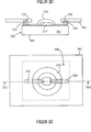
Die
LED-Vorrichtung in
Vorrichtungen
des Stands der Technik versuchen, die Einschränkungen der Substratgröße zu überwinden,
indem sie auf einer sekundären
Wärmesenke
in der Form der PCB
Zusätzlich erfordern
diese Lösungen
des Stands der Technik einen guten Kontakt zwischen der PCB und
dem Substrat
Die
vorliegende Erfindung liefert eine Hochleistungs-LED-Vorrichtung, die
eine ausreichende Wärmeableitfähigkeit
aufweist, um Fluktuationen bei der aus der LED abgegebenen Wärme zu absorbieren.
Zusätzlich
dissipiert die vorliegende Erfindung Wärme, ohne auf sekundären Wärmesenken
zu beruhen. Im folgenden wird Bezug auf die
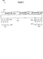
Um
die Drahtbondverbindungsoperation zu erleichtern, umfassen die Leiterbahnen
Im
folgenden wird Bezug auf die
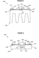
Die
LED-Vorrichtung
Ein
Körper
Es
wird angemerkt, dass die Wärmeübertragungsfähigkeit
der vorliegenden Erfindung durch ein Einschließen einer Oberfläche, die
eine größere Oberflächenfläche aufweist,
anstelle der Oberfläche
Die
oben beschriebenen Ausführungsbeispiele
verwenden einen Körper,
der eine flache Oberfläche
aufweist, wie z. B. die Oberfläche
Die
oben beschriebenen Ausführungsbeispiele
der vorliegenden Erfindung verwenden eine Einkapselungsschicht zum
Schutz der LED und der Bonddrähte.
Ausführungsbeispiele,
die einen Formring verwenden, um diesen Einkapselungsvorgang zu
unterstützen,
können
ebenso beinhaltet sein. Nun wird Bezug auf die
Der
ringförmig
geformte Ring
Es
wird angemerkt, dass die Oberfläche
Die
oben beschriebenen Ausführungsbeispiele
verwenden Bonddrähte
zur Herstellung aller Verbindungen zwischen der LED und den Lötmittelhöckern, die
eine Verbindung zu der PCB herstellen. Der Körper kann jedoch für eine dieser
Verbindungen verwendet werden. Wenn der Chip leitfähig ist
oder die Unterseite des Chips, der die LED aufweist, einen Kontakt
an demselben aufweist, und wenn der Chip an dem Körper durch
ein elektrisch leitendes Haftmittel angebracht ist, kann der Körper verwendet
werden, um eine Verbindung zu diesem Kontakt herzustellen. In diesem
Fall ist ein geeignet platzierter Lötmittelhöcker direkt auf der Oberfläche
Die
oben beschriebenen Ausführungsbeispiele
verwenden eine passive Konvektion/Konduktion zur Bewegung der Wärme von
der unteren Oberfläche
des Körpers,
z. B. der Oberfläche
Aus der vorangegangenen Beschreibung ist klar, dass bei einer LED-Vorrichtung gemäß der vorliegenden Erfindung der Körper sich über die Vorrichtungsstandfläche erstreckt. Deshalb weist die LED-Vorrichtung eine Wärmesenke auf, die die volle Standfläche der Vorrichtung nutzt. Zusätzlich ist der Körper nicht in einer Art thermisch isolierender Einkapselung eingeschlossen und deshalb in der Lage, Wärme wirksamer zu dissipieren. Ferner wurden Probleme in Bezug auf die Koplanarität der Anschlussleitungen und der Wärmesenke bei Vorrichtungen des Stands der Technik überwunden.Out It is clear from the foregoing description that in an LED device according to the present Invention of the body over the device footprint extends. Therefore, the LED device has a heat sink on that the full footprint the device uses. additionally is the body not included in a kind of thermally insulating encapsulation and therefore able to heat to dissipate more effectively. There were also problems regarding the coplanarity the connecting cables and the heat sink overcome in devices of the prior art.
Die untere Oberfläche des Körpers liegt gegenüber der Umgebung frei und so kann eine effiziente Wärmedissipierung erzielt werden. Zusätzlich kann der Körper, da die untere Oberfläche nicht in Kontakt mit einer anderen Oberfläche gelangt, derart hergestellt werden, dass sich diese Oberfläche so weit oder so tief wie möglich erstreckt. So ist es nun möglich, Vorrichtungen mit langen oder tiefen Wärmesenken herzustellen, ohne die lateralen Abmessungen der Vorrichtungen erhöhen zu müssen.The lower surface of the body lies opposite the environment free and so efficient heat dissipation can be achieved. In addition, can the body, because the bottom surface does not come into contact with another surface, thus prepared Be that surface as far or as deep as possible extends. So it is now possible To make devices with long or deep heat sinks, without to increase the lateral dimensions of the devices.
Ferner kann, da eine LED-Vorrichtung gemäß der vorliegenden Erfindung keine Wärme zu dem Anbringungssubstrat leiten muss, das Anbringungssubstrat aus üblichen Materialien aufgebaut sein, wie z. B. denjenigen, die in billigen PCBs eingesetzt werden. Zusätzlich muss der Endbenutzer keine zusätzliche Wärmesenke bereitstellen, wobei so der Entwurf von Produkten, die die LED-Vorrichtung verwenden, vereinfacht wird.Further can, as an LED device according to the present invention no heat to the attachment substrate, the attachment substrate from usual Be constructed materials such. B. those in cheap PCBs are used. additionally the end user does not need any extra heat sink providing the design of products using the LED device, is simplified.
Die
oben beschriebenen Ausführungsbeispiele
der vorliegenden Erfindung wurden in Bezug auf ein Übertragen
der durch die LED erzeugten Wärme über einen
Kontakt zwischen der Luft und der zweiten Oberfläche des Körpers, auf der die LED angebracht
ist, an die Luft beschrieben. Die vorliegende Erfindung kann jedoch
verwendet werden, um Produkte aufzubauen, die eine Anzahl von LEDs
auf einer einzelnen PCB aufweisen, die die in jeder der LEDs erzeugte
Wärme an
eine gemeinsame Wärmesenke übertragen,
die die Wärme
dissipiert. Nun wird Bezug auf
Bei den oben beschriebenen Ausführungsbeispielen ist der Chip auf einem wärmeleitenden Körper angebracht, der vorzugsweise aus Aluminium oder Kupfer hergestellt ist. Andere Materialien, wie z. B. Keramiken und Verbundstoffe, können jedoch für den wärmeleitenden Körper eingesetzt werden.at the embodiments described above the chip is mounted on a thermally conductive body, which is preferably made of aluminum or copper. Other Materials, such. As ceramics and composites, but can for the thermally conductive body be used.
Claims (16)
Applications Claiming Priority (2)
| Application Number | Priority Date | Filing Date | Title |
|---|---|---|---|
| US10/683,489 | 2003-10-09 | ||
| US10/683,489 US20050077616A1 (en) | 2003-10-09 | 2003-10-09 | High power light emitting diode device |
Publications (2)
| Publication Number | Publication Date |
|---|---|
| DE102004044149A1 DE102004044149A1 (en) | 2005-06-02 |
| DE102004044149B4 true DE102004044149B4 (en) | 2011-02-17 |
Family
ID=33160036
Family Applications (1)
| Application Number | Title | Priority Date | Filing Date |
|---|---|---|---|
| DE102004044149A Expired - Fee Related DE102004044149B4 (en) | 2003-10-09 | 2004-09-13 | High-performance light emitting diode device |
Country Status (4)
| Country | Link |
|---|---|
| US (2) | US20050077616A1 (en) |
| JP (1) | JP2005117041A (en) |
| DE (1) | DE102004044149B4 (en) |
| GB (1) | GB2406969B (en) |
Families Citing this family (53)
| Publication number | Priority date | Publication date | Assignee | Title |
|---|---|---|---|---|
| US7397067B2 (en) * | 2003-12-31 | 2008-07-08 | Intel Corporation | Microdisplay packaging system |
| JP4632427B2 (en) * | 2004-03-31 | 2011-02-16 | シーアイ化成株式会社 | Method for assembling light emitting diode assembly and light emitting diode assembly |
| JP4632426B2 (en) * | 2004-03-31 | 2011-02-16 | シーアイ化成株式会社 | Method for assembling light emitting diode assembly and light emitting diode assembly |
| TWM271255U (en) * | 2004-10-08 | 2005-07-21 | Bright Led Electronics Corp | High-power surface-mounted light-emitting diode with high heat dissipation property |
| US7262438B2 (en) * | 2005-03-08 | 2007-08-28 | Avago Technologies Ecbu Ip (Singapore) Pte. Ltd. | LED mounting having increased heat dissipation |
| KR100593937B1 (en) * | 2005-03-30 | 2006-06-30 | 삼성전기주식회사 | Led package using si substrate and fabricating method thereof |
| ES2822277T3 (en) * | 2005-05-20 | 2021-04-30 | Signify Holding Bv | Light emitting module |
| EP1890343A4 (en) * | 2005-06-07 | 2014-04-23 | Fujikura Ltd | Substrate for light-emitting device mounting, light-emitting device module, illuminating device, display and traffic signal device |
| KR100592508B1 (en) * | 2005-07-15 | 2006-06-26 | 한국광기술원 | High power led package with beacon type substrate |
| JP5155540B2 (en) * | 2005-09-20 | 2013-03-06 | パナソニック株式会社 | Light emitting device |
| JP5155539B2 (en) * | 2005-09-20 | 2013-03-06 | パナソニック株式会社 | Light emitting device |
| US20080099777A1 (en) * | 2005-10-19 | 2008-05-01 | Luminus Devices, Inc. | Light-emitting devices and related systems |
| CN101852349B (en) * | 2005-12-22 | 2012-08-29 | 松下电器产业株式会社 | Lighting apparatus with led |
| KR101210090B1 (en) | 2006-03-03 | 2012-12-07 | 엘지이노텍 주식회사 | Metal core printed circuit board and light-emitting diode packaging method thereof |
| US20070247852A1 (en) * | 2006-04-21 | 2007-10-25 | Xiaoping Wang | Multi chip LED lamp |
| TWI306674B (en) * | 2006-04-28 | 2009-02-21 | Delta Electronics Inc | Light emitting apparatus |
| CN101449391B (en) | 2006-05-30 | 2011-02-23 | 株式会社藤仓 | A base plate for mounting a luminous element, a light source, a lighting device, a display device, a piece of traffic signalling equipment and a manufacturing method of the base plate for mounting the |
| US20080068807A1 (en) * | 2006-09-20 | 2008-03-20 | Sunonwealth Electric Machine Industry Co., Ltd. | Heat-dissipating device for back light source for flat panel display |
| US9243794B2 (en) | 2006-09-30 | 2016-01-26 | Cree, Inc. | LED light fixture with fluid flow to and from the heat sink |
| US7686469B2 (en) | 2006-09-30 | 2010-03-30 | Ruud Lighting, Inc. | LED lighting fixture |
| US20090086491A1 (en) | 2007-09-28 | 2009-04-02 | Ruud Lighting, Inc. | Aerodynamic LED Floodlight Fixture |
| US9028087B2 (en) | 2006-09-30 | 2015-05-12 | Cree, Inc. | LED light fixture |
| US7952262B2 (en) * | 2006-09-30 | 2011-05-31 | Ruud Lighting, Inc. | Modular LED unit incorporating interconnected heat sinks configured to mount and hold adjacent LED modules |
| JP4238907B2 (en) * | 2006-10-18 | 2009-03-18 | セイコーエプソン株式会社 | Inkjet recording device |
| EP1914470B1 (en) * | 2006-10-20 | 2016-05-18 | OSRAM GmbH | Semiconductor lamp |
| TW200904316A (en) * | 2007-07-13 | 2009-01-16 | Kai-Yu Lin | Heat-dissipation structure of luminous device |
| JP5149601B2 (en) * | 2007-11-27 | 2013-02-20 | パナソニック株式会社 | Light emitting device |
| CN101465395A (en) * | 2007-12-21 | 2009-06-24 | 富士迈半导体精密工业(上海)有限公司 | Led |
| JP5416975B2 (en) * | 2008-03-11 | 2014-02-12 | ローム株式会社 | Semiconductor light emitting device |
| US7923746B2 (en) * | 2008-03-12 | 2011-04-12 | Industrial Technology Research Institute | Light emitting diode package structure and method for fabricating the same |
| CN101539282B (en) * | 2008-03-19 | 2011-06-29 | 富准精密工业(深圳)有限公司 | Light-emitting diode module |
| JP2009239036A (en) * | 2008-03-27 | 2009-10-15 | Hitachi Aic Inc | Led substrate |
| RU2471611C2 (en) * | 2008-08-18 | 2013-01-10 | Дзе Жиллетт Компани | Combined device for shaving and trimming |
| DE102008039364A1 (en) * | 2008-08-22 | 2010-03-04 | Osram Gesellschaft mit beschränkter Haftung | Semiconductor light emitting device |
| MX2009011735A (en) * | 2008-10-28 | 2010-08-12 | Abl Ip Holding Llc | Light emitting diode luminaires and applications thereof. |
| JP2010130001A (en) * | 2008-12-01 | 2010-06-10 | Kuei-Fang Chen | Radiation bed |
| KR101035335B1 (en) * | 2009-03-24 | 2011-05-23 | 김강 | Light Emitting Diode Package |
| US20100305448A1 (en) * | 2009-05-26 | 2010-12-02 | Anne Cecile Dagonneau | Apparatus and method for indicating ultrasound probe orientation and activation status |
| CN102032475A (en) * | 2009-08-23 | 2011-04-27 | 彭云滔 | Combined type high-power LED lamp |
| US8602593B2 (en) * | 2009-10-15 | 2013-12-10 | Cree, Inc. | Lamp assemblies and methods of making the same |
| US8089086B2 (en) * | 2009-10-19 | 2012-01-03 | Avago Technologies Ecbu Ip (Singapore) Pte. Ltd. | Light source |
| JP5645392B2 (en) * | 2009-11-30 | 2014-12-24 | 京セラ株式会社 | Parts for photoelectric conversion device and photoelectric conversion device |
| US8399267B2 (en) * | 2009-12-26 | 2013-03-19 | Achrolux Inc | Methods for packaging light emitting devices and related microelectronic devices |
| KR101677105B1 (en) * | 2010-08-30 | 2016-11-17 | 삼성디스플레이 주식회사 | Electronic component and manufacturing method for the same |
| US8354684B2 (en) * | 2011-01-09 | 2013-01-15 | Bridgelux, Inc. | Packaging photon building blocks having only top side connections in an interconnect structure |
| US8652860B2 (en) | 2011-01-09 | 2014-02-18 | Bridgelux, Inc. | Packaging photon building blocks having only top side connections in a molded interconnect structure |
| CN102683507A (en) * | 2011-03-09 | 2012-09-19 | 神基科技股份有限公司 | Light source module structure and producing method of light source module |
| CN102691921A (en) * | 2011-03-22 | 2012-09-26 | 展晶科技(深圳)有限公司 | Light-emitting diode light bar and method for manufacturing same |
| WO2013116114A1 (en) * | 2012-02-02 | 2013-08-08 | Bridgelux, Inc. | Packaging photon building blocks having only top side connections in a molded interconnect structure |
| US9538582B2 (en) | 2012-07-26 | 2017-01-03 | Taiwan Semiconductor Manufacturing Company, Ltd. | Warpage control in the packaging of integrated circuits |
| TWI571598B (en) * | 2015-01-15 | 2017-02-21 | 旭德科技股份有限公司 | Illumination apparatus |
| US9865528B2 (en) * | 2015-12-11 | 2018-01-09 | Ubotic Company Limited | High power and high frequency plastic pre-molded cavity package |
| CN108431489B (en) * | 2015-12-15 | 2021-07-06 | 株式会社小糸制作所 | Vehicle lamp |
Citations (6)
| Publication number | Priority date | Publication date | Assignee | Title |
|---|---|---|---|---|
| US5751060A (en) * | 1995-01-25 | 1998-05-12 | International Business Machines Corporation | Electronic package |
| US5910686A (en) * | 1998-07-23 | 1999-06-08 | Vlsi Technology, Inc. | Cavity down HBGA package structure |
| JPH11298048A (en) * | 1998-04-15 | 1999-10-29 | Matsushita Electric Works Ltd | Led mounting board |
| DE20117987U1 (en) * | 2001-10-23 | 2002-02-14 | Lite On Electronics Inc | Light-emitting diode device with low thermal resistance |
| WO2003019679A1 (en) * | 2001-08-28 | 2003-03-06 | Matsushita Electric Works, Ltd. | Light emitting device using led |
| US20030189830A1 (en) * | 2001-04-12 | 2003-10-09 | Masaru Sugimoto | Light source device using led, and method of producing same |
Family Cites Families (11)
| Publication number | Priority date | Publication date | Assignee | Title |
|---|---|---|---|---|
| JPS57155752A (en) | 1981-03-23 | 1982-09-25 | Hitachi Ltd | Resin sealed semiconductor device |
| US6011299A (en) * | 1996-07-24 | 2000-01-04 | Digital Equipment Corporation | Apparatus to minimize integrated circuit heatsink E.M.I. radiation |
| EP0926729A3 (en) * | 1997-12-10 | 1999-12-08 | Mitsubishi Gas Chemical Company, Inc. | Semiconductor plastic package and process for the production thereof |
| JP4432275B2 (en) * | 2000-07-13 | 2010-03-17 | パナソニック電工株式会社 | Light source device |
| JP3930710B2 (en) * | 2000-09-13 | 2007-06-13 | シチズン電子株式会社 | Chip-type light emitting diode and manufacturing method thereof |
| US6537857B2 (en) * | 2001-05-07 | 2003-03-25 | St Assembly Test Service Ltd. | Enhanced BGA grounded heatsink |
| JP2003008154A (en) * | 2001-06-21 | 2003-01-10 | Nec Corp | Printed wiring board, coaxial cable, and electronic device |
| WO2003030274A1 (en) * | 2001-09-27 | 2003-04-10 | Nichia Corporation | Light-emitting device and its manufacturing method |
| US7078803B2 (en) * | 2002-09-27 | 2006-07-18 | Isothermal Systems Research, Inc. | Integrated circuit heat dissipation system |
| US20040136163A1 (en) * | 2003-01-14 | 2004-07-15 | Sunonwealth Electric Machine Industry Co., Ltd. | Heat sink device having light-emitting components |
| US6864513B2 (en) * | 2003-05-07 | 2005-03-08 | Kaylu Industrial Corporation | Light emitting diode bulb having high heat dissipating efficiency |
-
2003
- 2003-10-09 US US10/683,489 patent/US20050077616A1/en not_active Abandoned
-
2004
- 2004-09-03 GB GB0419641A patent/GB2406969B/en not_active Expired - Fee Related
- 2004-09-13 DE DE102004044149A patent/DE102004044149B4/en not_active Expired - Fee Related
- 2004-10-04 JP JP2004291171A patent/JP2005117041A/en active Pending
-
2006
- 2006-02-20 US US11/358,477 patent/US7612386B2/en not_active Expired - Fee Related
Patent Citations (7)
| Publication number | Priority date | Publication date | Assignee | Title |
|---|---|---|---|---|
| US5751060A (en) * | 1995-01-25 | 1998-05-12 | International Business Machines Corporation | Electronic package |
| JPH11298048A (en) * | 1998-04-15 | 1999-10-29 | Matsushita Electric Works Ltd | Led mounting board |
| US5910686A (en) * | 1998-07-23 | 1999-06-08 | Vlsi Technology, Inc. | Cavity down HBGA package structure |
| US20030189830A1 (en) * | 2001-04-12 | 2003-10-09 | Masaru Sugimoto | Light source device using led, and method of producing same |
| WO2003019679A1 (en) * | 2001-08-28 | 2003-03-06 | Matsushita Electric Works, Ltd. | Light emitting device using led |
| US6930332B2 (en) * | 2001-08-28 | 2005-08-16 | Matsushita Electric Works, Ltd. | Light emitting device using LED |
| DE20117987U1 (en) * | 2001-10-23 | 2002-02-14 | Lite On Electronics Inc | Light-emitting diode device with low thermal resistance |
Also Published As
| Publication number | Publication date |
|---|---|
| GB2406969B (en) | 2008-04-23 |
| DE102004044149A1 (en) | 2005-06-02 |
| US20050077616A1 (en) | 2005-04-14 |
| JP2005117041A (en) | 2005-04-28 |
| US20060138645A1 (en) | 2006-06-29 |
| GB0419641D0 (en) | 2004-10-06 |
| US7612386B2 (en) | 2009-11-03 |
| GB2406969A (en) | 2005-04-13 |
Similar Documents
| Publication | Publication Date | Title |
|---|---|---|
| DE102004044149B4 (en) | High-performance light emitting diode device | |
| EP1547163B1 (en) | Optoelectronic component | |
| DE10351934B4 (en) | Light-emitting diode arrangement with heat dissipating board | |
| DE112006001634B4 (en) | A method of manufacturing a surface-mountable electric light emitting device having a heat sink | |
| DE102004009998B4 (en) | A light emitting diode and light emitting diode device comprising a light emitting diode | |
| DE10159695B4 (en) | A high luminous flux emitting diode having a light emitting diode of the flip-chip type with a transparent substrate | |
| DE102004033106B4 (en) | System and method for improved thermal LED conductivity | |
| DE102007019809B4 (en) | Housed circuit with a heat-dissipating lead frame and method of packaging an integrated circuit | |
| DE19500422A1 (en) | Semiconductor component with high heat emission | |
| WO2016034540A1 (en) | Light-emitting diode component | |
| DE102006038099A1 (en) | Light emitting device | |
| DE102007033057A1 (en) | Carrier strip based packages for solid state light emitting devices and methods of making carrier strip based packages for solid state light emitting devices | |
| DE102008016458A1 (en) | Printed circuit board for use in e.g. lighting device, has heat dissipating element arranged in through-hole, and radiation source i.e. LED, arranged on heat dissipating element, where heat dissipating element is electrically conductive | |
| DE102012207519A1 (en) | METHOD FOR PRODUCING A BUILDING ELEMENT SUPPORT, AN ELECTRONIC ARRANGEMENT AND A RADIATION ARRANGEMENT AND COMPONENT SUPPORT, ELECTRONIC ARRANGEMENT AND RADIATION ARRANGEMENT | |
| WO2009132618A1 (en) | Surface-mounted led module and method for producing a surface-mounted led module | |
| EP2583318A1 (en) | Surface-mountable optoelectronic component and method for producing a surface-mountable optoelectronic component | |
| DE102006033175A1 (en) | electronics assembly | |
| EP2283525A2 (en) | Light-emitting chip and light-emitting apparatus having such a light-emitting chip | |
| DE102012006924A1 (en) | LED lighting module with uniform light output | |
| EP1839344B1 (en) | Light-emitting diode and led light source | |
| DE102013207111B4 (en) | Optoelectronic component | |
| DE102011107966B4 (en) | LED light module | |
| DE102016107249B4 (en) | Printed circuit board with a recess for an electrical component, system with the printed circuit board and method for manufacturing the printed circuit board | |
| EP1217664A2 (en) | Semiconductor lighting unit and method for producing the same | |
| DE102011000120B4 (en) | Electronic light emitting device and method for making the same |
Legal Events
| Date | Code | Title | Description |
|---|---|---|---|
| OP8 | Request for examination as to paragraph 44 patent law | ||
| 8127 | New person/name/address of the applicant |
Owner name: AVAGO TECHNOLOGIES ECBU IP (SINGAPORE) PTE. LTD., |
|
| 8128 | New person/name/address of the agent |
Representative=s name: DILG HAEUSLER SCHINDELMANN PATENTANWALTSGESELLSCHA |
|
| R020 | Patent grant now final |
Effective date: 20110619 |
|
| R082 | Change of representative |
Representative=s name: DILG HAEUSLER SCHINDELMANN PATENTANWALTSGESELL, DE |
|
| R081 | Change of applicant/patentee |
Owner name: INTELLECTUAL DISCOVERY CO., LTD., KR Free format text: FORMER OWNER: AVAGO TECHNOLOGIES ECBU IP (SINGAPORE) PTE. LTD., SINGAPORE, SG Effective date: 20130227 |
|
| R082 | Change of representative |
Representative=s name: DILG HAEUSLER SCHINDELMANN PATENTANWALTSGESELL, DE Effective date: 20130227 |
|
| R119 | Application deemed withdrawn, or ip right lapsed, due to non-payment of renewal fee |