DE102004038552B4 - voltage - Google Patents
voltage Download PDFInfo
- Publication number
- DE102004038552B4 DE102004038552B4 DE102004038552A DE102004038552A DE102004038552B4 DE 102004038552 B4 DE102004038552 B4 DE 102004038552B4 DE 102004038552 A DE102004038552 A DE 102004038552A DE 102004038552 A DE102004038552 A DE 102004038552A DE 102004038552 B4 DE102004038552 B4 DE 102004038552B4
- Authority
- DE
- Germany
- Prior art keywords
- voltage
- current
- comparison
- ref
- comparator according
- Prior art date
- Legal status (The legal status is an assumption and is not a legal conclusion. Google has not performed a legal analysis and makes no representation as to the accuracy of the status listed.)
- Withdrawn - After Issue
Links
Classifications
-
- H—ELECTRICITY
- H03—ELECTRONIC CIRCUITRY
- H03K—PULSE TECHNIQUE
- H03K5/00—Manipulating of pulses not covered by one of the other main groups of this subclass
- H03K5/22—Circuits having more than one input and one output for comparing pulses or pulse trains with each other according to input signal characteristics, e.g. slope, integral
- H03K5/24—Circuits having more than one input and one output for comparing pulses or pulse trains with each other according to input signal characteristics, e.g. slope, integral the characteristic being amplitude
- H03K5/2472—Circuits having more than one input and one output for comparing pulses or pulse trains with each other according to input signal characteristics, e.g. slope, integral the characteristic being amplitude using field effect transistors
-
- H—ELECTRICITY
- H03—ELECTRONIC CIRCUITRY
- H03K—PULSE TECHNIQUE
- H03K5/00—Manipulating of pulses not covered by one of the other main groups of this subclass
- H03K5/01—Shaping pulses
- H03K5/08—Shaping pulses by limiting; by thresholding; by slicing, i.e. combined limiting and thresholding
-
- G—PHYSICS
- G01—MEASURING; TESTING
- G01R—MEASURING ELECTRIC VARIABLES; MEASURING MAGNETIC VARIABLES
- G01R19/00—Arrangements for measuring currents or voltages or for indicating presence or sign thereof
- G01R19/165—Indicating that current or voltage is either above or below a predetermined value or within or outside a predetermined range of values
- G01R19/16566—Circuits and arrangements for comparing voltage or current with one or several thresholds and for indicating the result not covered by subgroups G01R19/16504, G01R19/16528, G01R19/16533
Landscapes
- Physics & Mathematics (AREA)
- Nonlinear Science (AREA)
- Manipulation Of Pulses (AREA)
- Measurement Of Current Or Voltage (AREA)
- Analogue/Digital Conversion (AREA)
Abstract
Spannungskomparator
zum Vergleich einer Vergleichsspannung (Udiff)
mit einer Schwelle, mit
– einem
ersten Spannungs-Strom-Wandler (1) zur Wandlung einer die Schwelle
bestimmenden Referenzspannung (Uref) in
einen von der Referenzspannung (Uref) abhängigen Referenzstrom
(Iref)
– einem zweiten Spannungs-Strom-Wandler
(2) zur Wandlung der Vergleichsspannung (Udiff)
in einen von der Vergleichsspannung (Udiff)
abhängigen
Vergleichsstrom (Iv),
– zwei Eingängen (IN–n,
IN–p),
an denen die Vergleichsspannung als Differenzspannung (Udiff) anliegt, und
– einer Ausgangsstufe (3) zur
Ausgabe eines digitalen Ausgangspegels, wobei der Ausgangspegel
von dem Referenzstrom (Iref) und dem Vergleichsstrom
(Iv) abhängig
ist.Voltage comparator for comparing a comparison voltage (U diff ) with a threshold, with
- A first voltage-current converter (1) for converting a reference voltage determining the threshold (U ref ) in one of the reference voltage (U ref ) dependent reference current (I ref )
- A second voltage-current converter (2) for converting the comparison voltage (U diff ) in one of the comparison voltage (U diff ) dependent comparison current (I v ),
- Two inputs (IN -n , IN -p ), where the comparison voltage is applied as a differential voltage (U diff ), and
- An output stage (3) for outputting a digital output level, wherein the output level of the reference current (I ref ) and the comparison current (I v ) is dependent.
Description
Die vorliegende Erfindung betrifft einen Spannungskomparator.The The present invention relates to a voltage comparator.
Spannungskomparatoren haben die Aufgabe, eine Vergleichsspannung mit einer Referenzspannung zu vergleichen und das Ergebnis dieses Vergleiches am Ausgang möglichst trägheitslos zu signalisieren. Analogkomparatoren wirken als Schnittstelle zwischen analogen und digitalen Funktionseinheiten. Das amplitudenanaloge Eingangssignal (Spannung) wird in ein binäres Ausgangssignal (Spannung) umgewandelt. Am Ausgang tritt entweder H-Pegel (High-Pegel, hohes Potential) oder L-Pegel (Low-Pegel, niedriges Potential) auf. Komparatorschaltkreise sind beispielsweise spezielle Verstärker, die entsprechend den Operationsverstärkern einen Differenzeingang und einen unsymmetrischen Ausgang aufweisen können. Die Ausgangsstufe des Komparators ist meist so ausgelegt, dass sie mit den Logikpegeln mehrerer digitaler Schaltkreisfamilien kompatibel ist. Das bedeutet, dass digitale Schaltkreise ohne Zwischenschalten weiterer Elemente vom Komparatorausgang ansteuerbar sind. Komparatoren können dabei ohne und mit Rückkopplung (Hysterese) betrieben werden.Voltage comparators have the task to compare a reference voltage with a reference voltage and to signal the result of this comparison at the output as inertia as possible. Analog comparators act as an interface between analog and digital functional units. The amplitude analog input signal (voltage) is converted into a binary output signal (voltage). At the output either H level (high level, high potential) or L level (low level, low potential) occurs. Comparator circuits are, for example special amplifiers corresponding to the operational amplifiers erenzeingang a Diff and may have a single-ended output. The output stage of the comparator is usually designed to be compatible with the logic levels of several digital circuit families. This means that digital circuits can be controlled by the comparator output without interposing further elements. Comparators can be operated without and with feedback (hysteresis).
Typische Komparatoranwendungen sind Schwellwertschalter (Pegeldetektoren), Fensterdiskriminatoren, Gleichrichterschaltungen für kleine Signale, Schmitt-Trigger und andere Kippschaltungen, die u.a. zur Flankenversteilerung und zur Umwandlung zeitveränderlicher, beispielsweise sinusförmiger Spannungen in eine Rechteckfolge angewendet werden.typical Comparator applications are threshold switches (level detectors), Window discriminators, rectifier circuits for small Signals, Schmitt triggers and other flip-flops, i.a. to Flank steepening and conversion time-variable, for example sinusoidal voltages be applied in a rectangular sequence.
Aus
der
Aufgabe der vorliegenden Erfindung ist es, einen Spannungskomparator anzugeben, der möglichst im Automobilbereich einsetzbar ist. Diese Aufgabe wird durch den Spannungskomparator mit den Merkmalen des Anspruchs 1 gelöst. Günstige Weiterbildungen und Ausgestaltungsformen sind jeweils Gegenstand von Unteransprüchen.task the present invention is to provide a voltage comparator the possible can be used in the automotive sector. This task is done by the Voltage comparator with the features of claim 1 solved. Cheap trainings and embodiments are the subject of dependent claims.
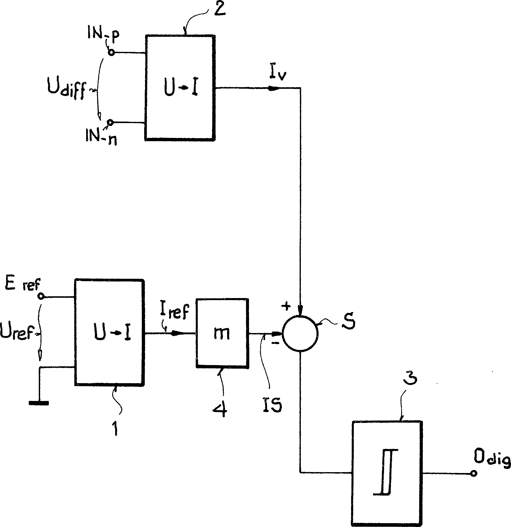
Gemäß der Erfindung wird anstelle eines Differenzverstärkers eine Komparatorfunktion durch zu vergleichende Ströme bereitgestellt. Demzufolge ist ein Spannungskomparator zum Vergleich einer Vergleichsspannung mit einer Schwelle vorgesehen. Der Spannungskomparator weist dabei vorzugsweise einen ersten Spannungs-Strom-Wandler zur Wandlung einer die Schwelle bestimmenden Referenzspannung in einen von der Referenzspannung abhängigen Referenzstrom auf. Im einfachsten Fall ist die Referenzspannung eine konstante Spannung, beispielsweise eine Zehnerspannung oder Versorgungsspannung. Bevorzugt ist die Referenzspannung jedoch eine einstellbare Spannung, beispielsweise eine analoge Ausgangsspannung eines Mikrocontrollers. Um den Referenzstrom zu generieren, wirkt der erste Spannungs-Strom-Wandler an seinem Ausgang vorteilhafterweise wie eine referenzspannungsabhängige Stromquelle mit einem Innenwiderstand.According to the invention becomes a comparator instead of a differential amplifier by streams to be compared provided. Consequently, a voltage comparator is for comparison a comparison voltage provided with a threshold. The voltage comparator preferably has a first voltage-current converter for Conversion of a threshold determining reference voltage in one dependent on the reference voltage Reference current on. In the simplest case, the reference voltage a constant voltage, for example, a voltage of ten or Supply voltage. However, the reference voltage is preferably one adjustable voltage, for example, an analog output voltage a microcontroller. To generate the reference current, acts the first voltage-current converter at its output advantageously like a reference voltage dependent Power source with an internal resistance.
Für den Spannungskomparator ist ein zweiter Spannungs-Strom-Wandler zur Wandlung der Vergleichsspannung in einen von der Vergleichsspannung abhängigen Vergleichsstrom erforderlich. Hinsichtlich des Vergleichsstromes wirkt der zweite Spannungs-Strom-Wandler an seinem Ausgang vorteilhafterweise wie eine vergleichsspannungsabhängige Stromquelle mit Innenwiderstand.For the voltage comparator is a second voltage-to-current converter for converting the comparison voltage in a comparison voltage dependent comparison current required. Regarding of the comparison current acts on the second voltage-current converter its output advantageously as a comparatively voltage-dependent current source with internal resistance.
An zwei Eingängen ist die Vergleichsspannung als Differenzspannung angelegt. Die Differenzspannung kann dabei von einer an beiden Eingängen anliegenden Gleichtakteingangsspannung signifikant abweichen.At two entrances the comparison voltage is applied as a differential voltage. The difference voltage can from a voltage applied to both inputs common mode input voltage differ significantly.
Weiterhin weist der Spannungskomparator eine Ausgangsstufe zur Ausgabe eines digitalen Ausgangspegels auf, wobei der Ausgangspegel von dem Referenzstrom und dem Vergleichsstrom abhängig ist. Die Abhängigkeit des Ausgangspegels bildet dabei die Komparatorfunktion ab, indem beispielsweise ein erster Ausgangspegel (high) einer Vergleichsspannung oberhalb einer ersten Schwelle zugeordnet ist und ein zweiter Ausgangspegel (low) einer Vergleichsspannung unterhalb einer zweiten Schwelle zugeordnet ist, wobei die erste und die zweite Schwelle gleich oder unterschiedlich sein können und beispielsweise eine Funktion eines Fensterkomparators abbilden.Farther the voltage comparator has an output stage for outputting a digital output level, wherein the output level of the reference current and the comparison current is. The dependence of the output level forms the comparator function by For example, a first output level (high) of a reference voltage is assigned above a first threshold and a second output level (Low) a comparison voltage below a second threshold is assigned, wherein the first and the second threshold equal or can be different and, for example, map a function of a window comparator.
Eine vorteilhafte Ausgestaltung der Erfindung sieht vor, dass die Ausgangsstufe mit einem Stromsummationsknoten verbunden ist, in dem sich der Vergleichsstrom und ein von dem Referenzstrom abhängiger Schwellenstrom summieren, wobei einer der beiden Ströme als negativer Wert in die Summation eingeht. Die Summe der in den Stromsummationsknoten hinein und heraus fließenden Ströme ist dabei stets null. Die Beziehung der Abhängigkeit zwischen dem Schwellenstrom und dem Referenzstrom ist dabei durch eine mathematische Funktion gegeben.A advantageous embodiment of the invention provides that the output stage is connected to a current summing node in which the comparison current and summing a threshold current dependent on the reference current, being one of the two streams entered as a negative value in the summation. The sum of in the Current summation node in and out flowing currents is always zero. The Relationship of dependence between the threshold current and the reference current is through given a mathematical function.
In einer Weiterbildung der Erfindung sind Mittel zur Multiplikation des Referenzstromes mit einem Multiplikationsfaktor vorgesehen, so dass der mittels des Multiplikationsfaktors generierte Schwellenstrom in die Summation im Stromsummationsknoten eingeht. Beispielsweise kann zum Vervielfachen des Stromes ein Mehrfaches des Referenzstromes zum Schwellenstrom mittels NMOS- oder PMOS-Transistoren geschalten werden. Zur Weiterbildung der Erfindung ist hierzu ein Referenzstromspiegel vorgesehen, dessen Stromspiegelverhältnis als Mittel zur Multiplikation einstellbar, insbesondere schaltbar ist. Beispielsweise können mehrere Transistoren, die den gespiegelten Strom des Referenzstromspiegels steuern parallel geschalten sein. Zur Einstellung des Multiplikationsfaktors werden einer oder mehrere dieser steuernden Transistoren aktiviert beziehungsweise deaktiviert, indem beispielsweise deren Gate-Potential verändert wird.In A development of the invention are means for multiplication the reference current is provided with a multiplication factor, such that the threshold current generated by the multiplication factor in the summation is received in the stream summation node. For example, can for multiplying the current, a multiple of the reference current switched to the threshold current by means of NMOS or PMOS transistors become. For further development of the invention, this is a reference current mirror provided, whose current mirror ratio as a means of multiplication adjustable, in particular switchable. For example, several Transistors that control the mirrored current of the reference current mirror be connected in parallel. For setting the multiplication factor one or more of these controlling transistors are activated or deactivated, for example, by their gate potential changed becomes.
Eine bevorzugte Ausgestaltung der Erfindung sieht vor, dass der Ausgangspegel durch ein Potential im Stromsummationsknoten bestimmt ist, das von dem Vergleichsstrom und dem Schwellenstrom abhängig ist. Bevorzugt ist der Spannungskomparator dabei derart dimensioniert, dass sich das Potential im Stromsummationsknoten in dem Bereich signifikant ändert, in dem Werte des Vergleichsstroms und des Schwellenstroms nahe beieinander liegen. Bevorzugt ist das Potential im Stromsummationsknoten dabei unabhängig von elektrischen Eigenschaften der Ausgangsstufe, diese weist hierzu vorteilhafterweise einen hochohmigen Eingang auf.A preferred embodiment of the invention provides that the output level is determined by a potential in the current summation node, that of the comparison current and the threshold current is dependent. Preferably, the Voltage comparator dimensioned so that the potential in the stream summation node in the area changes significantly, in the values of the comparison current and the threshold current are close to each other. In this case, the potential in the current summation node is preferably independent of electrical properties of the output stage, this has this advantageously a high-impedance input.
Vorzugsweise werden die Ausgangstufe und nachfolgende digitale Auswerteschaltkreise und vorzugsweise auch der die Spannungsreferenz generierende Schaltkreis mit Transistoreigenschaften für geringe Durchbruchspannungen von 10V hergestellt. Geringe Durchbruchsspannungen ermöglichen eine kleine Strukturbreite, die eine hohe Integrationsdichte insbesondere für digitale Auswerteschaltungen oder Kommunikationsschaltungen ermöglicht. In einer besonders bevorzugten Weiterbildung der Erfindung ist daher ein Spannungsbegrenzungsmittel zur Begrenzung der zwischen dem Stromsummationsknoten und dem Masseanschluss liegenden Spannung vorgesehen.Preferably become the output stage and subsequent digital evaluation circuits and preferably also the voltage reference generating circuit with transistor properties for low breakdown voltages of 10V produced. Low breakdown voltages enable a small structure width, which is a high integration density in particular for digital Evaluation circuits or communication circuits allows. In a particularly preferred embodiment of the invention is therefore a voltage limiting means for limiting the between the current summation node and the ground terminal voltage provided.
Ein Beispiel für ein derartiges Spannungsbegrenzungsmittel ist eine entsprechend mit dem Stromsummationsknoten und dem Masseanschluss verbundene Zehnerdiode. Oberhalb der Zehnerspannung fließt durch die Zehnerdiode ein zusätzlicher Zehnerstrom aus dem Stromsummationsknoten. Ohne einen Zehnerstrom ist in einer vorteilhaften, weiterbildenden Ausgestaltung der Erfindung vorgesehen, dass der Stromsummationsknoten über zumindest einen (zweiten) Transistor mit einem, mit dem zweiten Spannungs-Strom-Wandler verbundenen Stromspiegel verbunden ist. Dabei weist dieser, als Spannungsbegrenzungsmittel wirkende Transistor gegenüber der Ausgangsstufe eine höhere Durchbruchsspannungsfestigkeit auf. Insbesondere die hohe Durchbruchsspannungsfestigkeit dieses Transistors ermöglicht die Verwendung des Spannungskomparators als integrierter Bestandteil in einer Schaltung in einer so genannten Smart-Power-Technologie für den Einsatz in einem Kraftfahrzeug mit einer 42V Bordnetzspannung. Vorzugsweise weist dieser Transistor hierzu eine Durchbruchsspannungsfestigkeit von 80V auf.One example for such a voltage limiting means is a corresponding connected to the current summing node and the ground terminal Zener diode. Above the Zener voltage flows in through the Zener diode additional power of ten from the stream summation node. Without a power of ten is in one advantageous refinement of the invention, that the stream summation node over at least one (second) transistor with one, with the second Voltage-current converter connected current mirror is connected. In this case, this, acting as a voltage limiting means transistor across from the output stage has a higher breakdown voltage strength on. In particular, the high breakdown voltage strength of this transistor allows the use of the voltage comparator as an integral part in a circuit in a so-called smart-power technology for the Use in a motor vehicle with a 42V vehicle electrical system voltage. Preferably For this purpose, this transistor has a breakdown voltage strength from 80V up.
Der als Spannungsbegrenzungsmittel wirkende Transistor ist hierbei vorzugsweise als Emitterfolger geschaltet. So ist vorteilhafterweise das Gate beziehungsweise die Basis dieses Transistors mit der Versorgungsspannung der Ausgangsstufe verbunden oder verbindbar.Of the acting as a voltage limiting means transistor is in this case preferably switched as emitter follower. So is advantageously the gate or the base of this transistor with the supply voltage of the output stage connected or connectable.
Werden auch Referenzspannungen größer als die maximal zulässige Spannung in der Ausgangsstufe benötigt, ist in einer vorteilhaften Ausgestaltung der Erfindung vorgesehen, dass der Stromsummationsknoten über einen anderen Transistor mit dem ersten Spannungs-Strom-Wandler verbunden ist, wobei dieser, als Spannungsbegrenzungsmittel wirkende Transistor ebenfalls gegenüber der Ausgangsstufe eine höhere Durchbruchsspannungsfestigkeit aufweist. Vorzugsweise ist ebenfalls das Gate beziehungsweise die Basis dieses Transistors mit der Versorgungsspannung der Ausgangsstufe verbunden oder verbindbar.Become also reference voltages greater than the maximum allowable Voltage needed in the output stage is in a favorable one Embodiment of the invention provided that the current summation node via a another transistor connected to the first voltage-current converter is, with this, acting as a voltage limiting means transistor also opposite the output level is higher Has breakdown voltage strength. Preferably, too the gate or the base of this transistor with the supply voltage the output stage connected or connectable.
Eine vorteilhafte Ausgestaltung der Erfindung sieht vor, dass der erste Spannungs-Strom-Wandler und der zweite Spannungs-Strom-Wandler auf einem Halbleiterchip zueinander benachbart oder ineinander gesetzt angeordnet sind. Dies bewirkt, dass beide Wandler im Wesentlichen derselben Betriebstemperatur in diesem Bereich des Halbleiterchips ausgesetzt sind. Zudem sind die Auswirkungen von Fertigungstoleranzen, die über die Gesamtfläche eines Halbleiterchips auftreten in diesem Bereich der benachbarten oder ineinander verschachtelten Wandler nur gering. Dieses so genannte „matching" der beiden Wandlerstrukturen auf dem Halbleiterchip wird besonders vorteilhaft angewendet, indem der erste Spannungs-Strom-Wandler und der zweite Spannungs-Strom-Wandler gleiche Bauelemente aufweisen. Dies ermöglicht ein sehr ähnliches Verhalten der beiden Wandler auf physikalische Effekte, wie Temperaturänderungen oder mechanische Spannungen.A advantageous embodiment of the invention provides that the first Voltage-current converter and the second voltage-current converter a semiconductor chip adjacent to each other or into each other are arranged. This causes both transducers essentially same operating temperature in this region of the semiconductor chip are exposed. In addition, the effects of manufacturing tolerances, the above the total area a semiconductor chip occur in this area of the adjacent or interleaved converter only slightly. This so-called "matching" of the two converter structures The semiconductor chip is used particularly advantageously by the first voltage-to-current converter and the second voltage-to-current converter have the same components exhibit. this makes possible a very similar one Behavior of the two transducers on physical effects, such as temperature changes or mechanical stresses.
Eine bevorzugte und besonders einfache Ausgestaltung der Erfindung wird realisiert, indem zumindest einer der beiden Spannungs-Strom-Wandler einen Stromspiegel mit zumindest einem in Reihe geschalteten Widerstand aufweist. Mit der Annahme im Wesentlichen linearer Widerstände kann demzufolge oberhalb einer oder mehrerer Thresholdspannungen des Stromspiegels ein im Wesentlichen lineares Verhalten des Spannungs-Strom-Wandler angenommen werden. Für Spannungen unterhalb der Thresholdspannung verbleibt der Spannungs-Strom-Wandler inaktiv, so dass nur ein sehr geringer Ruhestrom im inaktiven Zustand benötigt wird.A preferred and particularly simple embodiment of the invention is realized by at least one of the two voltage-current converter to a current mirror with at least one resistor connected in series has. With the assumption of essentially linear resistances, therefore, a substantially linear behavior of the voltage-current converter can be assumed above one or more threshold voltages of the current mirror. For voltages below the threshold voltage of the voltage-current converter remains inactive, so that only a very low quiescent current is required in the inactive state.
Bevorzugt ist in einer Ausgestaltungsvariante der Erfindung vorgesehen, dass zusätzlich zum Referenzstrom und zum Vergleichstrom Mittel zur Generierung eines, vorzugsweise vom Referenzstrom abhängigen Querstroms vorgesehen sind, wobei der Querstrom einmal negativ und einmal positiv in die Summation im Stromsummationsknoten eingeht.Prefers is provided in an embodiment variant of the invention that additionally to the reference current and to the comparison current means for generating a, preferably dependent on the reference current cross-current provided are, with the cross-flow once negative and once positive in the Summation in the stream summation node is received.
Ändert sich die Vergleichsspannung im Bereich der Schwelle in einem Zeitbereich nur sehr langsam, ändert sich das Potential unter Umständen ebenfalls nur langsam zwischen dem binären Wert 0 und dem binären Wert 1. Vorzugsweise weist daher die Ausgangsstufe einen Schmitt-Trigger auf, dessen Eingang mit dem Stromsummationsknoten verbunden ist.Changes the comparison voltage in the range of the threshold in a time domain only very slowly, changes the potential may also be only slowly between the binary Value 0 and the binary Value 1. Preferably, therefore, the output stage has a Schmitt trigger whose input connected to the stream summation node.
Die Erfindung weiterbildend ist vorteilhafterweise vorgesehen, dass der zweite Spannungs-Strom-Wandler zur Wandlung einer positiven und einer negativen Differenzspannung ausgebildet ist, wobei der zweite Spannungs-Strom-Wandler hierzu vorzugsweise einen ersten, der positiven Differenzspannung zugeordneten Stromspiegel und einen zweiten, der negativen Differenzspannung zugeordneten Stromspiegel aufweist.The Further development of the invention is advantageously provided that the second voltage-to-current converter for converting a positive and a negative differential voltage is formed, wherein the second Voltage-current converter for this purpose preferably a first, the positive Differential voltage associated current mirror and a second, the having negative differential voltage associated current mirror.
Um in ein Strommanagement eines Kraftfahrzeugs auch den Komparator einzubeziehen, ist vorteilhafterweise ein Mittel zur Abschaltung der Versorgungsspannung der Ausgangsstufe vorgesehen, so dass der Spannungskomparator zwischen einem Schlafmodus und einem Betriebsmodus schaltbar ist.Around in a power management of a motor vehicle and the comparator is to be included, is advantageously a means of shutdown the supply voltage of the output stage provided, so that the Voltage comparator between a sleep mode and an operating mode is switchable.
Ein besonderer Aspekt der Erfindung ist eine Verwendung eines zuvor beschriebenen Spannungskomparators innerhalb einer Schaltung zur Auswertung und/oder Überwachung einer, mittels einer Ladungspumpe generierten Spannung.One particular aspect of the invention is a use of a previously described voltage comparator within a circuit for Evaluation and / or monitoring a voltage generated by a charge pump.
Ein weiterer Aspekt der Erfindung ist ein Analog-Digital-Umsetzer insbesondere nach dem Wägeverfahren oder nach dem Zählverfahren zur Umsetzung von einem zeitlichen Vergleichsspannungsverlauf in digitale Ausgangssignale mit einem zuvor beschriebenen Spannungskomparator.One Another aspect of the invention is an analog-to-digital converter in particular after the weighing process or after the counting process for the implementation of a temporal comparison voltage curve in digital output signals with a previously described voltage comparator.
Die Erfindung soll nachfolgend durch Ausführungsbeispiele im Zusammenhang mit zwei schematisierten Zeichnungen erläutert werden.The Invention is intended below by embodiments in connection be explained with two schematic drawings.
Im Einzelnen zeigtin the Individual shows
In
Dem
ersten Spannungs-Strom-Wandler
Weiterhin
ist ein zweiter Spannungs-Strom-Wandler
Weiterhin
ist der Stromsummationsknoten S mit einer Ausgangsstufe
Für einen
niedrigen Vergleichsstrom Iv wird der Stromfluss
durch den Stromsummationsknoten S durch den Vergleichstrom Iv bestimmt. Der erste Multiplikator
Wird
die Differenzspannung Udiff weiter erhöht, verbleibt
der durch den Stromsummationsknoten S fließende Strom im wesentlichen
konstant. Dadurch, dass der zweite Spannungs-Strom-Wandler
Dieser
zweite Spannungs-Strom-Wandler
Die
Ausgangssignale der Ausgangsstufe
Die
Ausgangsstufe
Die
Die
PMOS-Transistoren MP5 bis MP8 und die Widerstände R3, R4 des ersten Spannungs-Strom-Wandlers
Um
eine Einsatzmöglichkeit
für ein
42V Bordnetz eines Kraftfahrzeugs zu erhalten sind zumindest die
PMOS-Transistoren MP1 bis MP4 als Hochvolt-PMOS-Transistoren mit
einer Durchbruchsspannungsfestigkeit von 80V ausgelegt. Die Ausgangsstufe
Versucht
der zweite Spannungs-Strom-Wandler
Die Referenzspannung Uref wird in diesem Ausführungsbeispiel von Außen an den Spannungskomparator angelegt. Vorzugsweise sind die Bauelemente des Spannungskomparators auf einem Halbleiterchip integriert, wobei die Referenzspannung Uref an einen Anschluss des Halbleiterchips anschließbar ist. Alternativ ist es natürlich auch möglich die Referenzspannung Uref innerhalb des Spannungskomparators zu generieren.The reference voltage U ref is applied in this embodiment from the outside to the voltage comparator. Preferably, the components of the voltage comparator are integrated on a semiconductor chip, wherein the reference voltage U ref is connectable to a terminal of the semiconductor chip. Alternatively, it is of course also possible to generate the reference voltage U ref within the voltage comparator.
Neben
dem Vergleichsstrom Iv und dem Schwellenstrom
Is geht ein weiterer Strom IQ in die Summation
im Stromsummationsknoten S ein. Dieser Strom kann als Querstrom
IQ bezeichnet werden, der sowohl positiv
als auch negativ in die Stromsummation im Stromsummationsknoten
S eingeht und damit durch den Stromsummationsknoten S lediglich hindurch
fließt.
In dem Ausführungsbeispiel
der
- 1, 21, 2
- Spannungs-Strom-WandlerVoltage-current converter
- 33
- Ausgangsstufeoutput stage
- 44
- Multiplikatormultiplier
- Udif U dif
- Differenzspannungdifferential voltage
- IN–p, IN–n IN -p , IN -n
- Komparatoreingängecomparator inputs
- Uref U ref
- Referenzspannungreference voltage
- Eref E ref
- Eingang der Referenzspannungentrance the reference voltage
- Iv I v
- Vergleichsstromcomparison current
- Iref I ref
- Referenzstromreference current
- Is I s
- Schwellenstromthreshold current
- SS
- StromsummationsknotenCurrent summing node
- Odig O dig
- Komparatorausgangcomparator output
- VPVP
- Versorgungsspannungsanschluss 5VSupply voltage connection 5V
- VN, GNDVN, GND
- MasseDimensions
- MP1 bis MP10MP1 to MP10
- PMOS-TransistorPMOS transistor
- MN1 bis MN8MN1 to MN8
- NMOS-TransistorNMOS transistor
- R1 bis R4R1 to R4
- Widerstandresistance
- IQ IQ
- Querstromcrossflow
- STST
- Schmitt-TriggerSchmitt trigger
- INVINV
- Inverterinverter
Claims (21)
Priority Applications (4)
| Application Number | Priority Date | Filing Date | Title |
|---|---|---|---|
| DE102004038552A DE102004038552B4 (en) | 2004-08-06 | 2004-08-06 | voltage |
| EP05016721A EP1624567B1 (en) | 2004-08-06 | 2005-08-02 | Voltage comparator |
| DE502005008898T DE502005008898D1 (en) | 2004-08-06 | 2005-08-02 | voltage |
| US11/196,415 US7626427B2 (en) | 2004-08-06 | 2005-08-04 | Voltage comparator utilizing voltage to current conversion |
Applications Claiming Priority (1)
| Application Number | Priority Date | Filing Date | Title |
|---|---|---|---|
| DE102004038552A DE102004038552B4 (en) | 2004-08-06 | 2004-08-06 | voltage |
Publications (2)
| Publication Number | Publication Date |
|---|---|
| DE102004038552A1 DE102004038552A1 (en) | 2006-02-23 |
| DE102004038552B4 true DE102004038552B4 (en) | 2006-05-11 |
Family
ID=34982529
Family Applications (2)
| Application Number | Title | Priority Date | Filing Date |
|---|---|---|---|
| DE102004038552A Withdrawn - After Issue DE102004038552B4 (en) | 2004-08-06 | 2004-08-06 | voltage |
| DE502005008898T Active DE502005008898D1 (en) | 2004-08-06 | 2005-08-02 | voltage |
Family Applications After (1)
| Application Number | Title | Priority Date | Filing Date |
|---|---|---|---|
| DE502005008898T Active DE502005008898D1 (en) | 2004-08-06 | 2005-08-02 | voltage |
Country Status (3)
| Country | Link |
|---|---|
| US (1) | US7626427B2 (en) |
| EP (1) | EP1624567B1 (en) |
| DE (2) | DE102004038552B4 (en) |
Families Citing this family (6)
| Publication number | Priority date | Publication date | Assignee | Title |
|---|---|---|---|---|
| DE102006023934B3 (en) * | 2006-05-19 | 2007-11-15 | Atmel Germany Gmbh | Non-volatile memory device, has control circuit with switch to switch current depending on digital logic potential and with current-potential-transducer connected with outlet, where transducer charges control potential to control drift unit |
| DE602006013812D1 (en) | 2006-07-25 | 2010-06-02 | St Microelectronics Srl | Device for comparing the peak value of at least one voltage with a reference voltage |
| KR101057727B1 (en) * | 2009-05-15 | 2011-08-18 | 주식회사 하이닉스반도체 | Nonvolatile memory device |
| US8350599B2 (en) * | 2010-03-18 | 2013-01-08 | Aptus Power Semiconductors | Voltage comparators |
| US10797500B2 (en) * | 2016-09-20 | 2020-10-06 | Richtek Technology Corporation | Charger circuit and capacitive power conversion circuit and charging control method thereof |
| US11909359B2 (en) | 2021-10-07 | 2024-02-20 | Macom Technology Solutions Holdings, Inc. | Enhanced current mirror for multiple supply voltages |
Citations (2)
| Publication number | Priority date | Publication date | Assignee | Title |
|---|---|---|---|---|
| US6008673A (en) * | 1997-09-30 | 1999-12-28 | Intel Corporation | High speed, low power, current mode comparator |
| EP1492232A1 (en) * | 2003-06-27 | 2004-12-29 | Dialog Semiconductor GmbH | Comparator with high-voltage inputs in an extended CMOS process for higher voltage levels |
Family Cites Families (26)
| Publication number | Priority date | Publication date | Assignee | Title |
|---|---|---|---|---|
| US4047059A (en) * | 1976-05-24 | 1977-09-06 | Rca Corporation | Comparator circuit |
| US4602168A (en) * | 1984-03-28 | 1986-07-22 | National Semiconductor Corporation | Low offset CMOS comparator circuit |
| US4607232A (en) * | 1985-04-01 | 1986-08-19 | Raytheon Company | Low voltage amplifier circuit |
| US4659944A (en) * | 1985-04-08 | 1987-04-21 | Motorola, Inc. | High voltage detection circuit |
| US5077491A (en) * | 1990-11-30 | 1991-12-31 | Motorola, Inc. | Low standby current comparator having a zero temperature coefficient with hysterisis |
| US5136184A (en) * | 1991-05-24 | 1992-08-04 | Analog Devices, Incorporated | Fast-acting current comparator |
| JP2882163B2 (en) * | 1992-02-26 | 1999-04-12 | 日本電気株式会社 | Comparator |
| US5276359A (en) * | 1993-02-02 | 1994-01-04 | Chiang Ting Chi | Current-input type interface circuit of a mouse |
| EP0627817B1 (en) * | 1993-04-30 | 1999-04-07 | STMicroelectronics, Inc. | Voltage comparator with bandgap based direct current summing and power supply switch using it |
| TW239190B (en) * | 1993-04-30 | 1995-01-21 | Philips Electronics Nv | |
| US5477170A (en) * | 1994-02-17 | 1995-12-19 | Nec Corporation | Comparator capable of preventing large noise voltage |
| DE4434180A1 (en) * | 1994-09-24 | 1996-03-28 | Teves Gmbh Alfred | Circuit arrangement for evaluating the output signal of an active sensor |
| KR100218306B1 (en) * | 1996-06-27 | 1999-09-01 | 구본준 | Voltage-current converter |
| FR2751488B1 (en) * | 1996-07-16 | 1998-10-16 | Sgs Thomson Microelectronics | POWER AMPLIFIER IN BICMOS TECHNOLOGY WITH OUTPUT STAGE IN MOS TECHNOLOGY |
| DE19638087C2 (en) * | 1996-09-18 | 1999-09-02 | Siemens Ag | CMOS comparator |
| JPH11163644A (en) * | 1997-11-26 | 1999-06-18 | Fujitsu Ltd | Output circuit using differential amplifier circuit |
| KR100293446B1 (en) * | 1997-12-30 | 2001-07-12 | 김영환 | Main amplifier |
| JP2947256B1 (en) * | 1998-03-12 | 1999-09-13 | 日本電気株式会社 | Voltage determination circuit and battery pack including the same |
| US5945852A (en) * | 1998-03-31 | 1999-08-31 | Motorola, Inc. | CMOS comparator output circuit with high gain and hysteresis |
| US6020768A (en) * | 1998-05-13 | 2000-02-01 | Oak Technology, Inc. | CMOS low-voltage comparator |
| JP2000138573A (en) * | 1998-10-30 | 2000-05-16 | Fujitsu Ltd | Differential input circuit |
| JP4660680B2 (en) * | 2000-01-19 | 2011-03-30 | エスティー‐エリクソン、ソシエテ、アノニム | Voltage level detection circuit |
| US6586972B2 (en) * | 2000-02-28 | 2003-07-01 | Valorbec, Limited Partnership | Transistor-mismatch-insensitive current comparator cell |
| US6724329B2 (en) * | 2002-04-24 | 2004-04-20 | Intel Corporation | Decision feedback equalization employing a lookup table |
| US6791372B2 (en) * | 2002-06-04 | 2004-09-14 | Intel Corporation | Active cascode differential latch |
| JP3971368B2 (en) * | 2003-11-18 | 2007-09-05 | 株式会社東芝 | A signal intensity detection circuit and an amplification factor control system using the same. |
-
2004
- 2004-08-06 DE DE102004038552A patent/DE102004038552B4/en not_active Withdrawn - After Issue
-
2005
- 2005-08-02 EP EP05016721A patent/EP1624567B1/en not_active Expired - Fee Related
- 2005-08-02 DE DE502005008898T patent/DE502005008898D1/en active Active
- 2005-08-04 US US11/196,415 patent/US7626427B2/en not_active Expired - Fee Related
Patent Citations (2)
| Publication number | Priority date | Publication date | Assignee | Title |
|---|---|---|---|---|
| US6008673A (en) * | 1997-09-30 | 1999-12-28 | Intel Corporation | High speed, low power, current mode comparator |
| EP1492232A1 (en) * | 2003-06-27 | 2004-12-29 | Dialog Semiconductor GmbH | Comparator with high-voltage inputs in an extended CMOS process for higher voltage levels |
Also Published As
| Publication number | Publication date |
|---|---|
| US20060028248A1 (en) | 2006-02-09 |
| DE102004038552A1 (en) | 2006-02-23 |
| US7626427B2 (en) | 2009-12-01 |
| EP1624567A1 (en) | 2006-02-08 |
| DE502005008898D1 (en) | 2010-03-11 |
| EP1624567B1 (en) | 2010-01-20 |
Similar Documents
| Publication | Publication Date | Title |
|---|---|---|
| DE102006015762B4 (en) | Analog-to-digital converter arrangement and method | |
| DE102013211551B4 (en) | SYSTEM AND METHOD FOR BOSTED SWITCHES | |
| EP1624567B1 (en) | Voltage comparator | |
| DE102005020803B4 (en) | Circuit arrangement with an amplifier arrangement and an offset compensation arrangement | |
| DE102012222882A1 (en) | gate drive circuit | |
| DE102018218700A1 (en) | Power conversion device | |
| DE102004027298B4 (en) | On-chip high pass filter with high time constant | |
| DE102011015498A1 (en) | Input circuit for an input module and method for operating an input circuit | |
| DE102008050001B4 (en) | Digital-to-analog converter | |
| DE102010043950A1 (en) | Autonomous battery balancing | |
| DE2925331C2 (en) | Integrated circuit with reusable connections | |
| DE69918394T2 (en) | Limiting circuit for an analogue amplifier | |
| DE10040092A1 (en) | Circuit arrangement for detecting an error state | |
| DE102010013958A1 (en) | Differential amplifier with a rail-to-rail input voltage range | |
| DE19838657A1 (en) | Load current detection circuit e.g. for power field effect transistor (IGFET) | |
| EP0957420B1 (en) | Clamping circuit | |
| WO2019086285A1 (en) | Polarity-reversal protection arrangement, method for operating the polarity-reversal protection arrangement and corresponding use | |
| WO1993023925A1 (en) | Schmitt-trigger | |
| DE102006016356A1 (en) | Circuit arrangement for glitch-free or glitch-reduced signal transmission between voltage ranges | |
| DE10146849A1 (en) | Process for generating an output voltage | |
| DE4020187A1 (en) | CONTROL CIRCUIT FOR A TRANSISTOR DEVICE | |
| DE102005059489B4 (en) | Circuit and method for input signal determination | |
| WO2008071366A2 (en) | Integrated semiconductor circuit | |
| EP0834116B1 (en) | Circuit for comparing two electrical quantities | |
| DE2306455A1 (en) | VOLTAGE FOLLOW-UP |
Legal Events
| Date | Code | Title | Description |
|---|---|---|---|
| OP8 | Request for examination as to paragraph 44 patent law | ||
| 8364 | No opposition during term of opposition | ||
| 8327 | Change in the person/name/address of the patent owner |
Owner name: ATMEL AUTOMOTIVE GMBH, 74072 HEILBRONN, DE |
|
| 8330 | Complete disclaimer |