DE102004014658B4 - Optical matrix vector multiplier - Google Patents
Optical matrix vector multiplier Download PDFInfo
- Publication number
- DE102004014658B4 DE102004014658B4 DE200410014658 DE102004014658A DE102004014658B4 DE 102004014658 B4 DE102004014658 B4 DE 102004014658B4 DE 200410014658 DE200410014658 DE 200410014658 DE 102004014658 A DE102004014658 A DE 102004014658A DE 102004014658 B4 DE102004014658 B4 DE 102004014658B4
- Authority
- DE
- Germany
- Prior art keywords
- matrix
- waveguides
- optical
- waveguide
- vector
- Prior art date
- Legal status (The legal status is an assumption and is not a legal conclusion. Google has not performed a legal analysis and makes no representation as to the accuracy of the status listed.)
- Expired - Fee Related
Links
Classifications
-
- G—PHYSICS
- G06—COMPUTING; CALCULATING OR COUNTING
- G06E—OPTICAL COMPUTING DEVICES; COMPUTING DEVICES USING OTHER RADIATIONS WITH SIMILAR PROPERTIES
- G06E1/00—Devices for processing exclusively digital data
Landscapes
- Engineering & Computer Science (AREA)
- Theoretical Computer Science (AREA)
- Physics & Mathematics (AREA)
- General Physics & Mathematics (AREA)
- Optical Modulation, Optical Deflection, Nonlinear Optics, Optical Demodulation, Optical Logic Elements (AREA)
Abstract
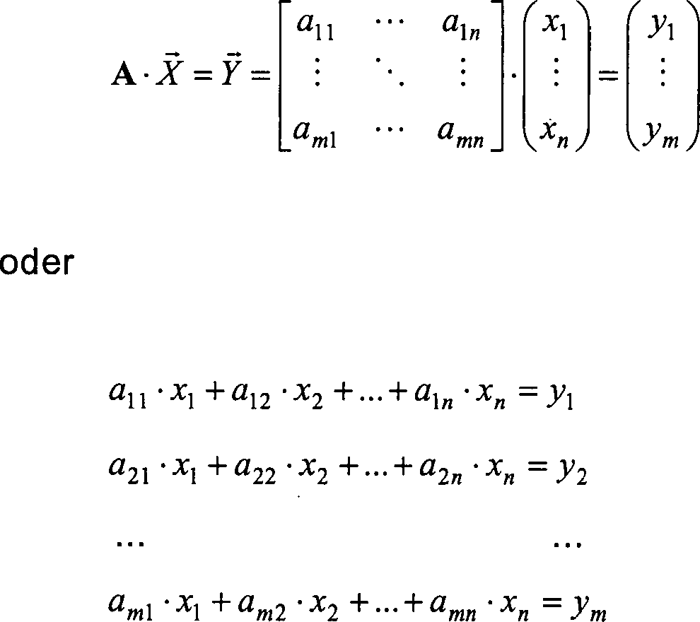
Optischer Vektor-Matrix Multiplizierer zur Durchführung einer Vektor-Matrix Multiplikation der Form A·X → = Y → zur Multiplikation von analogen Signalen, wobei A eine Matrix mit m·n Elementen, X → ein Vektor mit n Elementen und Y → ein Vektor mit m Elementen ist, wobei alle Elemente einen Definitionsbereich in einem Intervall der reellen Zahlen haben, umfassend:
extern eine Anzahl von n einzelnen, regelbaren Lichtquellen (5) für den Eingangsvektor X →,
extern eine Anzahl von n einzelnen optischen Detektoren (6) zum Auslesen des Ausgangsvektors Y →,
eine integrierte optische Anordnung der Multiplikationszellen auf einem Chip, einschließlich
einer Anzahl von n Eingangswellenleitern (1);
einer Anzahl von m Ausgangswellenleitern (3);
einer Anzahl von m·n Matrixwellenleitern (2),
wobei alle Eingangs-, Ausgangs- und Matrixwellenleiter (1, 3, 2) als planare Wellenleiter schichtweise übereinander aufgebaut sind,
wobei jeweils eine Zeile von m Matrixwellenleitern (2) eingangsseitig mit jeweils einem Eingangswellenleiter (1) gekoppelt ist und jeweils eine...Optical vector matrix multiplier for performing a vector matrix Multiplication of the form A · X → = Y → for multiplication of analog signals, where A is a matrix with m × n elements, X → a vector with n elements and Y → a vector with m elements, where all elements have a domain of definition in an interval of real numbers, comprising:
externally a number of n individual controllable light sources (5) for the input vector X →,
externally a number of n individual optical detectors (6) for reading out the output vector Y →,
an integrated optical arrangement of the multiplication cells on a chip, including
a number of n input waveguides (1);
a number of m output waveguides (3);
a number of m × n matrix waveguides (2),
wherein all input, output and matrix waveguides (1, 3, 2) are constructed in layers as planar waveguides,
wherein in each case one row of m matrix waveguides (2) is coupled on the input side to one input waveguide (1) and in each case one ...

Description
Gebiet der ErfindungField of the invention
Die Erfindung betrifft einen optischen Matrix-Vektor Multiplizierer, insbesondere einen als integriertes optisches Bauteil ausgebildeten Matrix-Vektor Multiplizierer.The The invention relates to an optical matrix vector multiplier, in particular designed as an integrated optical component Matrix vector multiplier.
Beschreibung des Standes der TechnikDescription of the state of technology
Mit der vorliegenden Erfindung lässt sich eine Matrix-Vekor Multiplikation durchführen, bei der ein n-dimensionaler Vektor X → mit einer m·n-dimensionalen Matrix A multipliziert wird. Als Ergebnis erhält man einen m-dimensionalen Vektor Y →.With of the present invention perform a matrix-vecor multiplication, in which an n-dimensional Vector X → with a mn-dimensional matrix A is multiplied. The result is an m-dimensional vector Y →.
Das
Standardverfahren um eine Matrix-Multiplikation auf optischem Weg
durchzuführen
besteht darin, dass man Lichtstrahlen durch eine optische Schicht
mit variabel einstellbarer Transparenz (z. B. LCD-Display) sendet
und die verbleibende Intensität
des Lichtes auf der anderen Seite der Schicht misst und als Ergebnis ausgibt.
Die Intensität
der eingekoppelten Lichtstahlen entspricht den Werten des Vektors X →.
Die Matrix A wird durch mm optische Elemente mit einstellbarer Transparenz
gebildet. Die Höhe
der Transparenz der einzelnen Elemente entspricht den Werten der
Matrix A. Nach diesem Prinzip arbeitende optische Vektor-Matrix
Multiplizierer finden sich zu Beispiel in
Neben
diesem Standardverfahren gibt es noch einige weniger verbreitete
Ansätze,
wie zum Beispiel die Verwendung von Freistrahloptik kombiniert mit
Hologrammen (
Von
allen diesen Lösungen
bilden die
Die
Die
Offenbarung der ErfindungDisclosure of the invention
Es ist die Aufgabe der Erfindung, einen optischen Matrix-Vektor Multiplizierer anzugeben, der in Form eines integriert-optischen Chips realisierbar ist und eine schnelle Multiplikation eines Vektors mit einer Matrix auf optischem Weg erlaubt. Der Multiplizierer soll ferner unempfindlich gegenüber temperaturbedingten Störeinflüssen sein.It The object of the invention is an optical matrix vector multiplier specify that can be realized in the form of an integrated-optical chip is and a fast multiplication of a vector with a matrix optical path allowed. The multiplier should also be insensitive across from be temperature-related disturbing influences.
Diese Aufgabe wird erfindungsgemäß durch einen Multiplizierer mit den Merkmalen des Patentanspruchs 1 gelöst.These Task is achieved by a multiplier with the features of claim 1 solved.
Bevorzugte Ausgestaltungen und vorteilhafte Merkmale der Erfindung sind in den abhängigen Patentansprüchen angegeben.preferred Embodiments and advantageous features of the invention are in the dependent claims specified.
Erfindungsgemäß umfasst der Vektor-Matrix Multiplizierer eine Anzahl von n Eingangswellenleitern, eine Anzahl von m Ausgangswellenleitern und eine Anzahl von m·n Matrixwellenleitern, wobei jeweils eine Zeile von m Matrixwellenleitern eingangsseitig mit jeweils einem Eingangswellenleiter gekoppelt ist und jeweils eine Spalte von n Matrixwellenleitern ausgangsseitig mit jeweils einem Ausgangswellenleiter gekoppelt ist. Jedem Matrixwellenleiter ist ein Modulator zugeordnet, das heißt insgesamt ist eine Anzahl von m·n Modulatoren vorgesehen. Ein wichtiges Merkmal der Erfindung ist die integriert-optische Anordnung insbesondere der Multiplikationszellen, auf einem Chip und die Ausnutzung der variablen Lichtabsorption über das quergedämpfte Feld am Außenrand der jeweiligen Matrix-Wellenleiter zur Modulation.According to the invention the vector matrix multiplier has a number of n input waveguides, one Number of m output waveguides and a number of m × n matrix waveguides, in each case one row of m matrix waveguides on the input side is coupled with one input waveguide and one each Column of n matrix waveguides on the output side with one each Output waveguide is coupled. Each matrix waveguide is a modulator is assigned, that is a total of a number of m · n Provided modulators. An important feature of the invention is the integrated-optical arrangement, in particular of the multiplication cells, on a chip and taking advantage of the variable light absorption over the cross-damped field on the outer edge the respective matrix waveguide for modulation.
Die
Hauptunterschiede gegenüber
dem Stand der Technik sind, dass
Es sind noch weitere Vorteile der Erfindung zu nennen:
- – Wenn der Matrixwellenleiter in der mittleren Schicht in einem (bogenförmigen) Winkel von der Seite an den unteren Eingangswellenleiter angenähert wird, können die Streuverluste reduziert werden.
- – Dadurch dass nur die Amplitude und nicht die Polarisation des Lichts für die Multiplikation verwendet wird, ist der Chip unempfindlich gegenüber temperaturinduzierten Spannungsfeldern, die zu Änderungen der Polarisation führen.
- – Wie bei allen planar-optischen Anordnungen kann man durch Ätzgruben die Position der Laser und Detektoren genau vorgeben, wodurch die exakte Positionierung dieser Elemente viel einfacher und billiger wird, als bei anderen Lösungsansätzen, die beispielsweise auf Freistrahloptik beruhen und wo die Ausrichtung der einzelnen Elemente sehr aufwendig ist.
- - When the matrix waveguide in the middle layer is approximated at an angle (arcuate) from the side to the lower input waveguide, the leakage losses can be reduced.
- By using only the amplitude and not the polarization of the light for the multiplication, the chip is insensitive to temperature-induced voltage fields which lead to changes of the polarization.
- As with all planar-optical arrangements, the position of the lasers and detectors can be accurately predicted by etching pits, making the exact positioning of these elements much easier and cheaper than other solutions based on, for example, free-beam optics and where the orientation of the individual elements very expensive.
Nachfolgend wird ein Ausführungsbeispiel der Erfindung anhand der Zeichnungen erläutert. Hierbei ergeben sich weitere Merkmale, Vorteile und Gestaltungsmöglichkeiten der Erfindung.following becomes an embodiment of the invention explained with reference to the drawings. This results Further features, advantages and design options of the invention.
Kurzbeschreibung der ZeichnungenBrief description of the drawings
Beschreibung eines bevorzugten Ausführungsbeispiels der ErfindungDescription of a preferred embodiment the invention
Um
eine Vektor-Matrix Multiplikation der Form 
Die einzelnen Multiplikationszellen der Matrix A sind dabei alle gleich aufgebaut. Aus Gründen der praktischen Realisierung sind jedoch die Zeilen und Spalten der Matrix vertauscht angeordnet. Die Matrixelemente einer Zeile, z. B. a11, a12, a13, ..., a1n, verlaufen nach unten, während die Elemente einer Spalte, z. B. a11, a21, a31, ..., am1, nach rechts verlaufen. Die einzelnen Elemente des Vektor X → = (x1, x2, x3, ..., xn) sind durch variable Lichtquellen realisiert. Als Lichtquellen können vorzugsweise einzelne Laserdioden bzw. ein Laserarray verwendet werden. Der Wert der Elemente x1, x2, x3, ..., xn wird durch die jeweilige von der Lichtquelle eingespeiste Lichtenergie bestimmt. Das Ergebnis der Multiplikation wird durch Detektoren ermittelt. Der Wert der detektierten Lichtenergie wird den jeweiligen Elementen des Ergebnisvektors Y → = (y1, y2, y3, ..., ym) zugeordnet.The individual multiplication cells of the matrix A are all the same structure. For reasons of practical implementation, however, the rows and columns of the matrix are arranged reversed. The matrix elements of a line, z. B. a 11 , a 12 , a 13 , ..., a 1n , run down, while the elements of a column, for. B. a 11 , a 21 , a 31 , ..., a m1 , to the right. The individual elements of the vector X → = (x 1 , x 2 , x 3 , ..., x n ) are realized by variable light sources. As light sources, preferably individual laser diodes or a laser array can be used. The value of the elements x 1 , x 2 , x 3 ,..., X n is determined by the respective light energy fed by the light source. The result of the multiplication is determined by detectors. The value of the detected light energy is assigned to the respective elements of the result vector Y → = (y 1 , y 2 , y 3 ,..., Y m ).
Um
das Prinzip des Multiplizierers zu erläutern schauen wir uns die Matrixzelle
a11 links oben in der Ecke an, da bei ihr
alle wesentlichen Elemente des Multiplizierers einschließlich Lichtquelle
und Detektor, vorhanden sind. Diese Zelle a11 ist
in den
Der
optische Chip ist schichtweise aufgebaut und umfasst übereinander
liegende Schichten, in denen mehrere planare Wellenleiter
Der
Abstand d zwischen den beiden Wellenleitern
In
einer weiteren Schicht des optischen Chips ist ein Ausgangswellenleiter
Jedem
Matrixwellenleiter
Der
Modulator
Alternativ
kann das Dämpfungselement
Das
Dämpfungselement
Die
Position der Modulatoren
Die
Ausgangswellenleiter
Eine
erfindungsgemäße Matrix-Vektor
Multiplikation wird nun an eines einfachen numerischen Beispiels
erläutert:
Es
wird angenommen, dass das System eine 2×2 Matrix mit einem zweidimensionalen
Vektor multiplizieren kann und 16 verschiedene Zustände für jeden
Eintrag (also Beispielsweise die positiven ganzen Zahlen von 0 bis
15) erlaubt.An inventive matrix-vector multiplication will now be explained by a simple numerical example:
It is assumed that the system can multiply a 2 × 2 matrix by a two-dimensional vector and allow 16 different states for each entry (eg, the positive integers from 0 to 15).
Unter
diesen Vorraussetzungen soll nun folgende einfache Matrix-Vektor
Multiplikation durchgeführt werden: ![]()
![]()
Das System kann 16 verschiedene Zustände unterscheiden. Das bedeutet, dass die Intensität der Lichtquelle 16 Intensitätsstufen (zwischen 0/16 = minimal und 16/16 = maximal) annehmen kann und die Absorptionselemente 16 verschiedene Absorptionsstärken von 0/16 = maximale Absorption bis 16/16 = minimale Absorption zulassen.The System can be 16 different states differ. This means that the intensity of the light source 16 intensity levels (between 0/16 = minimum and 16/16 = maximum) and the absorption elements 16 different absorption strengths of 0/16 = maximum absorption up to 16/16 = allow minimum absorption.
Die Werte des Eingangsvektors kodiert man, indem die dem ersten Vektorelement zugeordnete Lichtquelle auf 2/16 ihrer maximalen Leistung und die dem zweiten Vektorelement zugeordnete Lichtquelle auf 1/16 ihrer maximalen Leistung eingestellt wird. Bei der Matrix wird die Absorption der einzelnen Modulatoren so eingestellt, dass sie noch 2/16, 3/16, 1/16 und 4/16 des ankommenden Lichtes durchlassen.The Values of the input vector are encoded by the first vector element assigned light source to 2/16 of their maximum power and the the second vector element associated light source to 1/16 of her maximum power is set. In the case of the matrix, the absorption becomes of the individual modulators adjusted so that they are still 2/16, 3/16, Let through 1/16 and 4/16 of the incoming light.
Nehmen wir exemplarisch die Multiplikation des Vektorelements mit dem Wert 2 und dem ersten Matrixelement mit dem Wert 2. Der Vektorwert 2 wird durch 2/16 der maximalen Leistung der Lichtquelle kodiert und trifft dann auf den Modulator, der von dem ankommenden Licht noch 2/16 durchlässt, das heißt nach dem Modulator beträgt die Intensität des Lichts noch 4/256 des maximalen Wertes. Analog werden die übrigen Vektorelemente mit den entsprechenden Matrixelementen multipliziert und aufaddiert.To take we exemplify the multiplication of the vector element with the value 2 and the first matrix element with the value 2. The vector value 2 is coded by 2/16 of the maximum power of the light source and then hits the modulator, which still depends on the incoming light 2/16 lets through, this means after the modulator is the intensity of light still 4/256 of maximum value. The remaining vector elements become analog multiplied by the corresponding matrix elements and added up.
Bei der Interpretation der Intensität am Detektor muss man berücksichtigen, dass die Ergebniswerte auf den Maximalwert 256 normiert werden müssen, das heißt die Ergebniswerte werden mit 256 multipliziert, was elektronisch recht einfach realisiert werden kann. Dabei wird zum Beispiel die Maximalintensität von 15/256 auf den Wert 15 geeicht und Minimalintensität von 0/256 auf den Wert 0 geeicht.at the interpretation of the intensity at the detector you have to take into account that the result values must be normalized to the maximum value 256, the is called the result values are multiplied by 256, which is electronic quite easy to be realized. Here, for example, the maximum intensity calibrated from 15/256 to the value 15 and minimum intensity of 0/256 calibrated to the value 0.
Die
Multiplikation sieht damit folgendermaßen aus: 
Claims (13)
Priority Applications (1)
| Application Number | Priority Date | Filing Date | Title |
|---|---|---|---|
| DE200410014658 DE102004014658B4 (en) | 2004-03-25 | 2004-03-25 | Optical matrix vector multiplier |
Applications Claiming Priority (1)
| Application Number | Priority Date | Filing Date | Title |
|---|---|---|---|
| DE200410014658 DE102004014658B4 (en) | 2004-03-25 | 2004-03-25 | Optical matrix vector multiplier |
Publications (2)
| Publication Number | Publication Date |
|---|---|
| DE102004014658A1 DE102004014658A1 (en) | 2005-10-13 |
| DE102004014658B4 true DE102004014658B4 (en) | 2010-07-01 |
Family
ID=34982938
Family Applications (1)
| Application Number | Title | Priority Date | Filing Date |
|---|---|---|---|
| DE200410014658 Expired - Fee Related DE102004014658B4 (en) | 2004-03-25 | 2004-03-25 | Optical matrix vector multiplier |
Country Status (1)
| Country | Link |
|---|---|
| DE (1) | DE102004014658B4 (en) |
Cited By (2)
| Publication number | Priority date | Publication date | Assignee | Title |
|---|---|---|---|---|
| US10140720B1 (en) | 2016-12-30 | 2018-11-27 | X Development Llc | Integrated optical correlator |
| US11853871B2 (en) | 2018-06-05 | 2023-12-26 | Lightelligence PTE. Ltd. | Optoelectronic computing systems |
Families Citing this family (6)
| Publication number | Priority date | Publication date | Assignee | Title |
|---|---|---|---|---|
| CN101630178B (en) * | 2008-07-16 | 2011-11-16 | 中国科学院半导体研究所 | Silicon-based integrated optical vector-matrix multiplier |
| US9384168B2 (en) | 2013-06-11 | 2016-07-05 | Analog Devices Global | Vector matrix product accelerator for microprocessor integration |
| CN113159307A (en) | 2018-06-05 | 2021-07-23 | 光子智能股份有限公司 | Photoelectric computing system |
| US11734556B2 (en) | 2019-01-14 | 2023-08-22 | Lightelligence PTE. Ltd. | Optoelectronic computing systems |
| TWI806042B (en) | 2020-04-29 | 2023-06-21 | 新加坡商光子智能私人有限公司 | Optoelectronic processing apparatus, system and method |
| CN112490635B (en) * | 2020-11-05 | 2023-03-14 | 陕西飞机工业(集团)有限公司 | Matrix waveguide and airplane integrated integration method and system |
Citations (1)
| Publication number | Priority date | Publication date | Assignee | Title |
|---|---|---|---|---|
| US5448749A (en) * | 1989-11-22 | 1995-09-05 | Mitsubishi Denki Kabushiki Kaisha | Data processing apparatus with optical vector matrix multiplier and peripheral circuits |
-
2004
- 2004-03-25 DE DE200410014658 patent/DE102004014658B4/en not_active Expired - Fee Related
Patent Citations (1)
| Publication number | Priority date | Publication date | Assignee | Title |
|---|---|---|---|---|
| US5448749A (en) * | 1989-11-22 | 1995-09-05 | Mitsubishi Denki Kabushiki Kaisha | Data processing apparatus with optical vector matrix multiplier and peripheral circuits |
Non-Patent Citations (1)
| Title |
|---|
| M.Gruber et al.: "Planar-integrated optical vector-matrix multiplier", Applied Optics, Vol. 39, No. 29, 10. Oct. 2000, Pgs. 5367-5373 * |
Cited By (2)
| Publication number | Priority date | Publication date | Assignee | Title |
|---|---|---|---|---|
| US10140720B1 (en) | 2016-12-30 | 2018-11-27 | X Development Llc | Integrated optical correlator |
| US11853871B2 (en) | 2018-06-05 | 2023-12-26 | Lightelligence PTE. Ltd. | Optoelectronic computing systems |
Also Published As
| Publication number | Publication date |
|---|---|
| DE102004014658A1 (en) | 2005-10-13 |
Similar Documents
| Publication | Publication Date | Title |
|---|---|---|
| EP0340577B1 (en) | Method and device for determining the refractive index of a substance | |
| DE3149733C2 (en) | ||
| DE3609507C2 (en) | Fiber optic interferometer | |
| DE3345038A1 (en) | OPTICAL WAVE GUIDE DEVICE | |
| DE2804105C2 (en) | ||
| DE60203383T2 (en) | Total reflection optical switch with moving drop | |
| EP0795121A1 (en) | Process and device for measuring light beams | |
| DE102004014658B4 (en) | Optical matrix vector multiplier | |
| DE2529073C2 (en) | Coupling element for fiber optic light guides | |
| DE2527939C2 (en) | Method for operating a planar multimode optical waveguide | |
| DE60002421T2 (en) | Optical traveling wave modulators | |
| DE69734800T2 (en) | Fiber optic element, light receiving element, and pattern detection device | |
| EP0260594A2 (en) | Device for controlling light polarization, in particular in a heterodyne or homodyne optical receiver | |
| DE112020001819T5 (en) | DETECTING DEVICE AND METHOD FOR MANUFACTURING IT | |
| DE3201128A1 (en) | OPTICAL SWITCHING DEVICE | |
| DE3443863C2 (en) | ||
| CH628154A5 (en) | ARRANGEMENT FOR MODULATING THE LIGHT IN AN OPTICAL WAVE GUIDE FOR TRANSMISSION PURPOSES IN OPTICAL COMMUNICATION SYSTEMS. | |
| DE3101415A1 (en) | OPTICAL SWITCH | |
| DE60127146T2 (en) | OPTICAL DEVICE | |
| DE112017008247T5 (en) | Reflective spatial light modulator, optical observation device and light irradiation device | |
| DE1283963B (en) | Method for the controllable directional deflection of optical radiation, in particular laser radiation, and device for carrying out the same | |
| DE3024104A1 (en) | INTEGRATED MICRO-OPTICAL DEVICE FOR USE WITH MULTIMODE LIGHT FIBERS AND METHOD FOR THEIR PRODUCTION | |
| DE2359797C3 (en) | Switchable optical waveguide device | |
| DE112019000241T5 (en) | Stress-optical phase shifter array for lidar and other applications | |
| WO2022058307A1 (en) | Optical matrix multiplication unit for an optoelectronic system for forming an artificial neural network |
Legal Events
| Date | Code | Title | Description |
|---|---|---|---|
| 8110 | Request for examination paragraph 44 | ||
| 8364 | No opposition during term of opposition | ||
| R119 | Application deemed withdrawn, or ip right lapsed, due to non-payment of renewal fee |
Effective date: 20131001 |