CN211063818U - L ED lamp - Google Patents
L ED lamp Download PDFInfo
- Publication number
- CN211063818U CN211063818U CN201921179405.0U CN201921179405U CN211063818U CN 211063818 U CN211063818 U CN 211063818U CN 201921179405 U CN201921179405 U CN 201921179405U CN 211063818 U CN211063818 U CN 211063818U
- Authority
- CN
- China
- Prior art keywords
- circuit
- lamp
- capacitor
- base
- output
- Prior art date
- Legal status (The legal status is an assumption and is not a legal conclusion. Google has not performed a legal analysis and makes no representation as to the accuracy of the status listed.)
- Active
Links
Images


Classifications
-
- H—ELECTRICITY
- H05—ELECTRIC TECHNIQUES NOT OTHERWISE PROVIDED FOR
- H05B—ELECTRIC HEATING; ELECTRIC LIGHT SOURCES NOT OTHERWISE PROVIDED FOR; CIRCUIT ARRANGEMENTS FOR ELECTRIC LIGHT SOURCES, IN GENERAL
- H05B45/00—Circuit arrangements for operating light-emitting diodes [LED]
- H05B45/30—Driver circuits
- H05B45/37—Converter circuits
- H05B45/3725—Switched mode power supply [SMPS]
-
- H—ELECTRICITY
- H05—ELECTRIC TECHNIQUES NOT OTHERWISE PROVIDED FOR
- H05B—ELECTRIC HEATING; ELECTRIC LIGHT SOURCES NOT OTHERWISE PROVIDED FOR; CIRCUIT ARRANGEMENTS FOR ELECTRIC LIGHT SOURCES, IN GENERAL
- H05B45/00—Circuit arrangements for operating light-emitting diodes [LED]
- H05B45/30—Driver circuits
- H05B45/34—Voltage stabilisation; Maintaining constant voltage
-
- F—MECHANICAL ENGINEERING; LIGHTING; HEATING; WEAPONS; BLASTING
- F21—LIGHTING
- F21K—NON-ELECTRIC LIGHT SOURCES USING LUMINESCENCE; LIGHT SOURCES USING ELECTROCHEMILUMINESCENCE; LIGHT SOURCES USING CHARGES OF COMBUSTIBLE MATERIAL; LIGHT SOURCES USING SEMICONDUCTOR DEVICES AS LIGHT-GENERATING ELEMENTS; LIGHT SOURCES NOT OTHERWISE PROVIDED FOR
- F21K9/00—Light sources using semiconductor devices as light-generating elements, e.g. using light-emitting diodes [LED] or lasers
- F21K9/20—Light sources comprising attachment means
- F21K9/23—Retrofit light sources for lighting devices with a single fitting for each light source, e.g. for substitution of incandescent lamps with bayonet or threaded fittings
- F21K9/238—Arrangement or mounting of circuit elements integrated in the light source
-
- F—MECHANICAL ENGINEERING; LIGHTING; HEATING; WEAPONS; BLASTING
- F21—LIGHTING
- F21K—NON-ELECTRIC LIGHT SOURCES USING LUMINESCENCE; LIGHT SOURCES USING ELECTROCHEMILUMINESCENCE; LIGHT SOURCES USING CHARGES OF COMBUSTIBLE MATERIAL; LIGHT SOURCES USING SEMICONDUCTOR DEVICES AS LIGHT-GENERATING ELEMENTS; LIGHT SOURCES NOT OTHERWISE PROVIDED FOR
- F21K9/00—Light sources using semiconductor devices as light-generating elements, e.g. using light-emitting diodes [LED] or lasers
- F21K9/60—Optical arrangements integrated in the light source, e.g. for improving the colour rendering index or the light extraction
- F21K9/64—Optical arrangements integrated in the light source, e.g. for improving the colour rendering index or the light extraction using wavelength conversion means distinct or spaced from the light-generating element, e.g. a remote phosphor layer
-
- F—MECHANICAL ENGINEERING; LIGHTING; HEATING; WEAPONS; BLASTING
- F21—LIGHTING
- F21K—NON-ELECTRIC LIGHT SOURCES USING LUMINESCENCE; LIGHT SOURCES USING ELECTROCHEMILUMINESCENCE; LIGHT SOURCES USING CHARGES OF COMBUSTIBLE MATERIAL; LIGHT SOURCES USING SEMICONDUCTOR DEVICES AS LIGHT-GENERATING ELEMENTS; LIGHT SOURCES NOT OTHERWISE PROVIDED FOR
- F21K9/00—Light sources using semiconductor devices as light-generating elements, e.g. using light-emitting diodes [LED] or lasers
- F21K9/60—Optical arrangements integrated in the light source, e.g. for improving the colour rendering index or the light extraction
- F21K9/66—Details of globes or covers forming part of the light source
-
- F—MECHANICAL ENGINEERING; LIGHTING; HEATING; WEAPONS; BLASTING
- F21—LIGHTING
- F21V—FUNCTIONAL FEATURES OR DETAILS OF LIGHTING DEVICES OR SYSTEMS THEREOF; STRUCTURAL COMBINATIONS OF LIGHTING DEVICES WITH OTHER ARTICLES, NOT OTHERWISE PROVIDED FOR
- F21V29/00—Protecting lighting devices from thermal damage; Cooling or heating arrangements specially adapted for lighting devices or systems
- F21V29/10—Arrangement of heat-generating components to reduce thermal damage, e.g. by distancing heat-generating components from other components to be protected
-
- F—MECHANICAL ENGINEERING; LIGHTING; HEATING; WEAPONS; BLASTING
- F21—LIGHTING
- F21V—FUNCTIONAL FEATURES OR DETAILS OF LIGHTING DEVICES OR SYSTEMS THEREOF; STRUCTURAL COMBINATIONS OF LIGHTING DEVICES WITH OTHER ARTICLES, NOT OTHERWISE PROVIDED FOR
- F21V29/00—Protecting lighting devices from thermal damage; Cooling or heating arrangements specially adapted for lighting devices or systems
- F21V29/50—Cooling arrangements
- F21V29/70—Cooling arrangements characterised by passive heat-dissipating elements, e.g. heat-sinks
-
- H—ELECTRICITY
- H05—ELECTRIC TECHNIQUES NOT OTHERWISE PROVIDED FOR
- H05B—ELECTRIC HEATING; ELECTRIC LIGHT SOURCES NOT OTHERWISE PROVIDED FOR; CIRCUIT ARRANGEMENTS FOR ELECTRIC LIGHT SOURCES, IN GENERAL
- H05B45/00—Circuit arrangements for operating light-emitting diodes [LED]
- H05B45/30—Driver circuits
- H05B45/37—Converter circuits
-
- H—ELECTRICITY
- H05—ELECTRIC TECHNIQUES NOT OTHERWISE PROVIDED FOR
- H05K—PRINTED CIRCUITS; CASINGS OR CONSTRUCTIONAL DETAILS OF ELECTRIC APPARATUS; MANUFACTURE OF ASSEMBLAGES OF ELECTRICAL COMPONENTS
- H05K1/00—Printed circuits
- H05K1/02—Details
- H05K1/0201—Thermal arrangements, e.g. for cooling, heating or preventing overheating
- H05K1/0203—Cooling of mounted components
- H05K1/0204—Cooling of mounted components using means for thermal conduction connection in the thickness direction of the substrate
-
- H—ELECTRICITY
- H05—ELECTRIC TECHNIQUES NOT OTHERWISE PROVIDED FOR
- H05K—PRINTED CIRCUITS; CASINGS OR CONSTRUCTIONAL DETAILS OF ELECTRIC APPARATUS; MANUFACTURE OF ASSEMBLAGES OF ELECTRICAL COMPONENTS
- H05K1/00—Printed circuits
- H05K1/02—Details
- H05K1/0213—Electrical arrangements not otherwise provided for
- H05K1/0216—Reduction of cross-talk, noise or electromagnetic interference
- H05K1/0218—Reduction of cross-talk, noise or electromagnetic interference by printed shielding conductors, ground planes or power plane
-
- H—ELECTRICITY
- H05—ELECTRIC TECHNIQUES NOT OTHERWISE PROVIDED FOR
- H05K—PRINTED CIRCUITS; CASINGS OR CONSTRUCTIONAL DETAILS OF ELECTRIC APPARATUS; MANUFACTURE OF ASSEMBLAGES OF ELECTRICAL COMPONENTS
- H05K1/00—Printed circuits
- H05K1/02—Details
- H05K1/11—Printed elements for providing electric connections to or between printed circuits
- H05K1/111—Pads for surface mounting, e.g. lay-out
-
- H—ELECTRICITY
- H05—ELECTRIC TECHNIQUES NOT OTHERWISE PROVIDED FOR
- H05K—PRINTED CIRCUITS; CASINGS OR CONSTRUCTIONAL DETAILS OF ELECTRIC APPARATUS; MANUFACTURE OF ASSEMBLAGES OF ELECTRICAL COMPONENTS
- H05K1/00—Printed circuits
- H05K1/18—Printed circuits structurally associated with non-printed electric components
- H05K1/181—Printed circuits structurally associated with non-printed electric components associated with surface mounted components
-
- F—MECHANICAL ENGINEERING; LIGHTING; HEATING; WEAPONS; BLASTING
- F21—LIGHTING
- F21Y—INDEXING SCHEME ASSOCIATED WITH SUBCLASSES F21K, F21L, F21S and F21V, RELATING TO THE FORM OR THE KIND OF THE LIGHT SOURCES OR OF THE COLOUR OF THE LIGHT EMITTED
- F21Y2105/00—Planar light sources
- F21Y2105/10—Planar light sources comprising a two-dimensional array of point-like light-generating elements
- F21Y2105/14—Planar light sources comprising a two-dimensional array of point-like light-generating elements characterised by the overall shape of the two-dimensional array
- F21Y2105/18—Planar light sources comprising a two-dimensional array of point-like light-generating elements characterised by the overall shape of the two-dimensional array annular; polygonal other than square or rectangular, e.g. for spotlights or for generating an axially symmetrical light beam
-
- F—MECHANICAL ENGINEERING; LIGHTING; HEATING; WEAPONS; BLASTING
- F21—LIGHTING
- F21Y—INDEXING SCHEME ASSOCIATED WITH SUBCLASSES F21K, F21L, F21S and F21V, RELATING TO THE FORM OR THE KIND OF THE LIGHT SOURCES OR OF THE COLOUR OF THE LIGHT EMITTED
- F21Y2115/00—Light-generating elements of semiconductor light sources
- F21Y2115/10—Light-emitting diodes [LED]
-
- H—ELECTRICITY
- H05—ELECTRIC TECHNIQUES NOT OTHERWISE PROVIDED FOR
- H05B—ELECTRIC HEATING; ELECTRIC LIGHT SOURCES NOT OTHERWISE PROVIDED FOR; CIRCUIT ARRANGEMENTS FOR ELECTRIC LIGHT SOURCES, IN GENERAL
- H05B45/00—Circuit arrangements for operating light-emitting diodes [LED]
- H05B45/30—Driver circuits
- H05B45/36—Circuits for reducing or suppressing harmonics, ripples or electromagnetic interferences [EMI]
-
- H—ELECTRICITY
- H05—ELECTRIC TECHNIQUES NOT OTHERWISE PROVIDED FOR
- H05K—PRINTED CIRCUITS; CASINGS OR CONSTRUCTIONAL DETAILS OF ELECTRIC APPARATUS; MANUFACTURE OF ASSEMBLAGES OF ELECTRICAL COMPONENTS
- H05K2201/00—Indexing scheme relating to printed circuits covered by H05K1/00
- H05K2201/07—Electric details
- H05K2201/0707—Shielding
- H05K2201/0723—Shielding provided by an inner layer of PCB
-
- H—ELECTRICITY
- H05—ELECTRIC TECHNIQUES NOT OTHERWISE PROVIDED FOR
- H05K—PRINTED CIRCUITS; CASINGS OR CONSTRUCTIONAL DETAILS OF ELECTRIC APPARATUS; MANUFACTURE OF ASSEMBLAGES OF ELECTRICAL COMPONENTS
- H05K2201/00—Indexing scheme relating to printed circuits covered by H05K1/00
- H05K2201/10—Details of components or other objects attached to or integrated in a printed circuit board
- H05K2201/10007—Types of components
- H05K2201/1006—Non-printed filter
-
- H—ELECTRICITY
- H05—ELECTRIC TECHNIQUES NOT OTHERWISE PROVIDED FOR
- H05K—PRINTED CIRCUITS; CASINGS OR CONSTRUCTIONAL DETAILS OF ELECTRIC APPARATUS; MANUFACTURE OF ASSEMBLAGES OF ELECTRICAL COMPONENTS
- H05K2201/00—Indexing scheme relating to printed circuits covered by H05K1/00
- H05K2201/10—Details of components or other objects attached to or integrated in a printed circuit board
- H05K2201/10007—Types of components
- H05K2201/10106—Light emitting diode [LED]
-
- H—ELECTRICITY
- H05—ELECTRIC TECHNIQUES NOT OTHERWISE PROVIDED FOR
- H05K—PRINTED CIRCUITS; CASINGS OR CONSTRUCTIONAL DETAILS OF ELECTRIC APPARATUS; MANUFACTURE OF ASSEMBLAGES OF ELECTRICAL COMPONENTS
- H05K2201/00—Indexing scheme relating to printed circuits covered by H05K1/00
- H05K2201/10—Details of components or other objects attached to or integrated in a printed circuit board
- H05K2201/10007—Types of components
- H05K2201/10174—Diode
-
- H—ELECTRICITY
- H05—ELECTRIC TECHNIQUES NOT OTHERWISE PROVIDED FOR
- H05K—PRINTED CIRCUITS; CASINGS OR CONSTRUCTIONAL DETAILS OF ELECTRIC APPARATUS; MANUFACTURE OF ASSEMBLAGES OF ELECTRICAL COMPONENTS
- H05K2201/00—Indexing scheme relating to printed circuits covered by H05K1/00
- H05K2201/10—Details of components or other objects attached to or integrated in a printed circuit board
- H05K2201/10431—Details of mounted components
- H05K2201/10507—Involving several components
- H05K2201/10522—Adjacent components
-
- Y—GENERAL TAGGING OF NEW TECHNOLOGICAL DEVELOPMENTS; GENERAL TAGGING OF CROSS-SECTIONAL TECHNOLOGIES SPANNING OVER SEVERAL SECTIONS OF THE IPC; TECHNICAL SUBJECTS COVERED BY FORMER USPC CROSS-REFERENCE ART COLLECTIONS [XRACs] AND DIGESTS
- Y02—TECHNOLOGIES OR APPLICATIONS FOR MITIGATION OR ADAPTATION AGAINST CLIMATE CHANGE
- Y02B—CLIMATE CHANGE MITIGATION TECHNOLOGIES RELATED TO BUILDINGS, e.g. HOUSING, HOUSE APPLIANCES OR RELATED END-USER APPLICATIONS
- Y02B20/00—Energy efficient lighting technologies, e.g. halogen lamps or gas discharge lamps
- Y02B20/30—Semiconductor lamps, e.g. solid state lamps [SSL] light emitting diodes [LED] or organic LED [OLED]
Landscapes
- Engineering & Computer Science (AREA)
- Microelectronics & Electronic Packaging (AREA)
- General Engineering & Computer Science (AREA)
- Physics & Mathematics (AREA)
- Optics & Photonics (AREA)
- Electromagnetism (AREA)
- Circuit Arrangement For Electric Light Sources In General (AREA)
- Circuit Arrangements For Discharge Lamps (AREA)
Abstract
The utility model is suitable for a lamps and lanterns design technical field provides an L ED lamps and lanterns, L ED lamps and lanterns include circuit board and base, the base is hollow structure, the base lateral wall is including conductive parts, the circuit board sets up in the base, be equipped with L ED power drive circuit and L ED light source on the circuit board, L ED power drive circuit is including the full-bridge rectifier circuit that connects gradually, pi type filter circuit, non-isolator drive circuit's output and L ED light source are connected, full-bridge rectifier circuit, pi type filter circuit, non-isolator drive circuit connects formation power ground altogether, power ground is connected with conductive parts electricity, reduce the disturbance of the electromagnetic energy that high frequency switch signal arouses to other equipment, in order to shield electromagnetic interference.
Description
Technical Field
The embodiment of the utility model provides a belong to lamps and lanterns design technical field, especially relate to an L ED lamps and lanterns.
Background
With the development of the technology, L ED lamp tube products exist in the market, L ED driving power supplies are mainly divided into two types, namely a switching constant current source and a linear driving power supply, the linear driving technology has no high-frequency switch, the problem of electromagnetic compatibility does not exist On a metal circuit board (commonly used aluminum substrate, hereinafter, aluminum substrate for short), however, the switching driving technology can drive a switching tube (field effect tube MOS) to be closed and closed in high frequency in real time, the problem of electromagnetic compatibility exists On the metal circuit board (commonly used aluminum substrate), the standard requirements of main countries and regions On power supply terminal disturbance voltage and radiation electromagnetic disturbance cannot be met, for example, GB 17743-.
SUMMERY OF THE UTILITY MODEL
The embodiment of the utility model provides an L ED lamps and lanterns aims at solving the L ED lamp that satisfies the authentication standard and can't adopt the switch drive technique to realize that power drive sets up the design at metal circuit board DOB (driver On Board), and then can't satisfy the problem that wide input voltage's adjustment rate and product high efficiency were made simultaneously.
An embodiment of the utility model provides an L ED lamps and lanterns, including circuit board and base, the base is hollow structure, the base lateral wall is including conductive parts, the circuit board sets up in the base, be equipped with L ED power drive circuit and L ED light source on the circuit board, L ED power drive circuit is including full-bridge rectifier circuit, pi type filter circuit, the non-isolator drive circuit who connects gradually, non-isolator drive circuit's output with L ED light source connection, full-bridge rectifier circuit pi type filter circuit non-isolator drive circuit connects altogether and forms the power ground, the power ground with conductive parts electricity is connected.
The embodiment of the utility model provides an L ED lamps and lanterns, set up the circuit board in the base that has hollow structure, the base lateral wall is provided with conductive parts, be provided with L ED power drive circuit and L ED light source On the circuit board, L ED power drive circuit is including the full-bridge rectifier circuit that connects gradually, pi type filter circuit, non-isolator drive circuit's output and L ED light source are connected, full-bridge rectifier circuit, pi type filter circuit, non-isolator drive circuit are connected altogether and are formed power ground, power ground with conductive parts electricity is connected, realize that power ground is connected with the conductive parts electricity of lamps and lanterns base, lead the high frequency switch signal of power drive circuit to the metal conducting part of L ED lamps and lanterns base, reduce the electromagnetic energy that high frequency switch signal arouses and to the disturbance of other equipment, shielding electromagnetic interference, make L ED lamps and lanterns that satisfy the certification standard, can adopt switch drive technique to realize that the power drive sets up the design On circuit board DOB (driver) On, and then satisfied wide input voltage's regulation rate and manufacturing requirement, have stronger practicality and easy practicality and high efficiency.
Drawings
In order to more clearly illustrate the technical solutions in the embodiments of the present invention, the drawings needed to be used in the description of the embodiments will be briefly introduced below, and it is obvious that the drawings in the following description are some embodiments of the present invention, and for those skilled in the art, other drawings can be obtained according to these drawings without creative efforts.
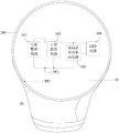
Fig. 1 is a schematic structural diagram of an L ED lamp provided by an embodiment of the present invention;
fig. 2 is a schematic diagram of an overall structure of an L ED lamp according to another embodiment of the present invention;
fig. 3 is a schematic structural diagram of an L ED power driving circuit according to an embodiment of the present invention;
fig. 4 is a schematic diagram of a specific structure of an L ED power driving circuit according to another embodiment of the present invention;
fig. 5 is a waveform diagram of experimental data of lamp No. 1 according to an embodiment of the present invention;
fig. 6 is a waveform diagram of experimental data of lamp No. 2 according to an embodiment of the present invention;
fig. 7 is a waveform diagram of experimental data of lamp No. 2 according to another embodiment of the present invention;
fig. 8 is a waveform diagram of experimental data of lamp No. 1 according to an embodiment of the present invention;
fig. 9 is a waveform diagram of experimental data of lamp No. 2 according to an embodiment of the present invention;
fig. 10 is a waveform diagram of experimental data of lamp No. 2 according to another embodiment of the present invention;
fig. 11 is a waveform diagram of experimental data of lamp No. 1 according to an embodiment of the present invention;
fig. 12 is a waveform diagram of experimental data of lamp No. 2 according to an embodiment of the present invention;
fig. 13 is a waveform diagram of experimental data of lamp No. 1 according to an embodiment of the present invention;
fig. 14 is a waveform diagram of experimental data of lamp No. 2 according to an embodiment of the present invention.
Detailed Description
In order to make the technical solution of the present invention better understood, the technical solution in the embodiments of the present invention will be clearly described below with reference to the accompanying drawings in the embodiments of the present invention, and it is obvious that the described embodiments are some embodiments of the present invention, not all embodiments. Based on the embodiments in the present invention, all other embodiments obtained by a person skilled in the art without creative efforts shall belong to the protection scope of the present invention.
The terms "comprises" and "comprising," and any variations thereof, in the description and claims of this invention and the above-described drawings are intended to cover non-exclusive inclusions. For example, a process, method, or system, article, or apparatus that comprises a list of steps or elements is not limited to only those steps or elements listed, but may alternatively include other steps or elements not listed, or inherent to such process, method, article, or apparatus. Furthermore, the terms "first," "second," and "third," etc. are used to distinguish between different objects and are not used to describe a particular order.
As shown in fig. 1, a structural schematic diagram of an L ED lamp according to an embodiment of the present invention is shown, and for convenience of illustration, only the portions related to the embodiment of the present invention are shown, which is described in detail as follows.
When the L ED lamp group is driven by the switch driving power supply, the switch tube is driven to be closed and turned off in a high-frequency mode in real time, if the switch driving power supply is arranged On a circuit board, the problem of electromagnetic compatibility exists due to disturbance voltage and radiation electromagnetism of a power supply terminal, the requirement of various countries or regions On the electromagnetic compatibility standard cannot be met, the driving power supply of the L ED lamp group meeting the quality certification cannot adopt the design that the driving power supply is arranged On a metal circuit board and the DOB (driver On Board), and further the adjustment rate of wide input voltage and the simplicity and the high efficiency of manufacturing a finished lamp group cannot be achieved.
As shown in the figure, the L ED lamp includes a circuit board 10 and a base 20, the base 20 is a hollow structure, the side wall of the base 20 includes a conductive part 201, the circuit board 10 is disposed in the base 20, the circuit board 10 is provided with a L ED power driving circuit and a L ED light source 104, the L ED power driving circuit includes a full-bridge rectifying circuit 101, a pi-type filter circuit 102 and a non-isolated switch driving circuit 103 which are connected in sequence, an output end of the non-isolated switch driving circuit 103 is connected with the L ED light source 104, the full-bridge rectifying circuit 101, the pi-type filter circuit 102 and the non-isolated switch driving circuit 103 are connected in common to form a power ground PE, and the power ground PE is.
Optionally, the base 20 further includes an outer insulating layer disposed on the periphery of the conductive member 201. It is understood that the edge of the circuit board 10 may abut against the top end of the conductive component, and may also abut against the step disposed on the top of the outer insulating layer, in this embodiment, the edge of the circuit board 10 preferably abuts against the top end of the conductive component 201 to improve the heat dissipation effect of the circuit board 10 during operation.
Optionally, the conductive member is an electroplated layer provided on an inner sidewall of the outer insulating layer. Optionally, in other embodiments, the base 20 may also include an outer insulating layer, a conductive layer, and an inner insulating layer stacked from outside to inside, where the conductive layer is the conductive part 201 and at least partially exposed in the inner insulating layer, and the conductive layer partially exposed in the inner insulating layer is electrically connected to a power supply, so as to guide the high-frequency switching signal to the conductive part 201 of the base 20, reduce interference of electromagnetic energy caused by the high-frequency switching signal to other devices, and perform an electromagnetic interference shielding function.
The circuit board 10 is a metal substrate circuit board, specifically an aluminum copper substrate, an aluminum iron substrate or an aluminum nickel substrate, the base 20 is a heat dissipation structure of L ED lamp, the outer wall of the base 20 is an outer insulation layer, when the light source power is high, the L ED lamp generates more heat, a conductive part 201 is added on the inner wall of the heat dissipation structure, the conductive part 201 can be an aluminum embedded part, the edge of the circuit board 10 can be in thermal connection with the aluminum embedded part, so that the heat can be rapidly conducted to the whole heat dissipation structure, the heat dissipation speed is accelerated, the conductive part 201 can also be made of other metals, such as copper, iron or stainless steel, etc., and the L ED light source 104 comprises a plurality of light emitting diodes.
As shown in fig. 2, an overall structure diagram of an L ED luminaire according to another embodiment of the present invention is shown, and for convenience of illustration, only the portions related to the embodiments of the present invention are shown, which are described in detail below.
The power ground formed by connecting the full-bridge rectifier circuit, the pi-type filter circuit and the non-isolated switch drive circuit in common is electrically connected to the conductive member 201 through the conductive terminal 30 or a wire.
Alternatively, the metal terminal 30 may include a first section having one end electrically connected to the circuit board 10 and a second section extending from the other end of the first section toward the sidewall of the circuit board 10; the second section is provided along the side edge of the circuit board 10, and when the circuit board 10 is fixedly connected to the inner wall of the base 20, the second section abuts against the inner wall of the base 20, so that the metal terminal 30 is electrically connected to the conductive member 201 on the inner wall of the base 20.
Optionally, the first section and the second section of the metal terminal 30 are integrally formed, the first section is perpendicular to the second section, the widths of the first section and the second section are equal, and the length of the first section is greater than that of the second section. Specifically, the size of the metal terminal 30 may be set according to the size of the circuit board, and is not particularly limited. One end of the first section of the metal terminal 30 is welded on the DOB circuit board, the other end is bent downwards along the edge of the circuit board, when the circuit board is installed in the base, the side edge of the circuit board is tightly sleeved on the inner side wall of the base, the other end of the metal terminal 30 bent downwards is clamped between the circuit board and the inner side wall of the base 20, and the metal terminal 30 is electrically connected with the conductive part 201 on the inner side wall of the base 20 in a contact mode.
It is understood that the L ED lamp further includes a base 40 and a light-transmitting bulb 50, the base 40 is disposed at one end of the base 20 and electrically connected to the circuit board, and the light-transmitting bulb 50 is disposed at the other end of the base 20.
According to the embodiment, the L ED power supply driving circuit is led out, the power supply ground is electrically connected with the conductive part of the base through the metal terminal or the lead, the switch driving power supply arranged on the circuit board effectively guides the high-frequency switch signal to the conductive part of the base when the high-frequency switch tube is driven to be closed and turned off, disturbance of electromagnetic energy caused by the high-frequency switch signal to other equipment is reduced, the electromagnetic interference shielding effect is achieved, the requirement on electromagnetic compatibility is met, and meanwhile the design of DOB and the simple and efficient performance of manufacturing a lamp set finished product are achieved through the switch driving technology.
As shown in fig. 3, a specific schematic structure diagram of an L ED power driving circuit according to an embodiment of the present invention is shown, and for convenience of illustration, only the portions related to the embodiment of the present invention are shown, which is described in detail as follows.
The L ED power driving circuit comprises a full bridge rectifying circuit 101, a pi-type filter circuit 102, a non-isolated switch driving circuit 103, a L ED light source 104 and a power ground 105.
The input end of the full-bridge rectification circuit 101 is used as the input anode of the L ED power supply driving circuit, the full-bridge rectification circuit 101 is connected with a power supply signal and outputs a voltage signal at the anode output end, and the cathode output end is connected with the ground.
The first input end of the pi-type filter circuit 102 is connected with the anode output end of the full-bridge rectification circuit 101, the first output end of the pi-type filter circuit 102 is connected with the output anode of the L ED power supply driving circuit, the second input end of the pi-type filter circuit 102 is connected with the ground, and the second output end of the pi-type filter circuit 102 is connected with the second input end of the non-isolated switch driving circuit 103.
The first input end of the non-isolated switch driving circuit 103 is connected with the first output end of the pi-type filter circuit 102, the first output end of the non-isolated switch driving circuit 103 is connected with L ED power supply driving circuit output anode, the second output end of the non-isolated switch driving circuit 103 is connected with L ED power supply driving circuit output cathode, and the grounding end of the non-isolated switch driving circuit 103 is connected with the ground.
L ED power drive circuit output positive pole connected L ED light source 104 positive pole, L ED power drive circuit output negative pole connected L ED light source 104 negative pole full bridge rectifier circuit 101, pi type filter circuit 102, non-isolated switch drive circuit 103 connected to form power ground 105.
Optionally, as shown in fig. 3, the pi filter circuit 102 includes a first inductor L1, a first capacitor C1, and a second capacitor C2, wherein a first end of the first inductor L1 is used as a first input end of the pi filter circuit 102, and a second end of the first inductor L1 is used as a first output end of the pi filter circuit 102.
A first terminal of the first inductor L1 is connected to a first terminal of the first capacitor C1, a second terminal of the first inductor L1 is connected to a first terminal of the second capacitor C2, a second terminal of the first capacitor C1 and a second terminal of the second capacitor C2 are commonly connected, and a second terminal of the first capacitor C1 and a second terminal of the second capacitor C2 are commonly connected to form a power ground PE.
Alternatively, as shown in fig. 4, in another embodiment of the present invention, a specific structural diagram of the L ED power driving circuit is provided, in which a first end of the first capacitor C1 is connected to a first end of the second capacitor C2 and serves as a first input end of the pi filter circuit 102, a second end of the second capacitor C2 is connected to a second end of the first inductor L1 and serves as a second output end of the pi filter circuit 102, a second end of the first capacitor C1 and the first end of the first inductor L1 are connected to the same ground, and the second end of the second capacitor C2 and the second end of the first inductor L1 are connected to the same ground to form the power ground PE.
Optionally, the first inductor L1 is a chip inductor of 3.0 millihenry, and the first capacitor C1 and the second capacitor C2 are chip electrolytic capacitors with a capacitance of 2.2 microfarads and a withstand voltage of 400 v.
Optionally, as shown in fig. 3 and fig. 4, in a specific structural diagram of the L ED power driving circuit, the non-isolated switch driving circuit 103 is a L ED constant current driving circuit with a BUCK architecture, and includes a diode D1, a first resistor R1, a second resistor R2, a third resistor R3, a second inductor L2, a third capacitor C3, and a driving chip U1.
The first pin of the driver chip U1 is used as the first input terminal of the non-isolated switch driver 103, the first terminal of the second inductor L2 is used as the second output terminal of the non-isolated switch driver, and the second terminal of the first resistor R1 and the second terminal of the second resistor R2 are used as the second input terminal of the non-isolated switch driver 103.
The anode of the diode D1 is connected to the second pin of the driver ic U1 and the second end of the second inductor L2, respectively, and the cathode of the diode D1 is connected to the output anode of the L ED power driver circuit.
The first end of a third capacitor C3 is connected with the output anode of the L ED power supply driving circuit, the second end of a third capacitor C3 is connected with the output cathode of the L ED power supply driving circuit, the first end of a third resistor R3 is connected with the output anode of the L ED power supply driving circuit, and the second end of a third resistor R3 is connected with the output cathode of the L ED power supply driving circuit.
A third pin of the driving chip U1 is connected to a first end of the first resistor R1 and a first end of the second resistor R2, respectively; the second end of the first resistor R1, the second end of the second resistor R2 and the fourth pin of the driving chip U1 are connected in common.
The full-bridge rectifier circuit is a full-bridge rectifier comprising four diodes. A thermal relay FR1 is also provided at the input of the rectifier circuit.
Specifically, through experimental data testing and comparison, lamps provided with two power supply driving circuits are marked as a lamp No. 1 and a lamp No. 2, no metal terminal is welded or a lead is arranged on a metal circuit board of the lamp No. 1, and a power ground of the L ED power supply driving circuit is not electrically connected with a conductive part of a base, a metal terminal is welded or a lead is arranged on a metal circuit board of the lamp No. 2, and the power ground of the L ED power supply driving circuit is connected with the conductive part of the base through the metal terminal or the lead to realize electrical connection (wherein, the specific structure of the L ED power supply driving circuit comprises the power supply driving circuits corresponding to the two pi-type filter circuits provided by the above embodiment), the two lamps are subjected to data testing according to different standards, and the following data results are obtained:
according to the EN55015 standard, test L perturbs the voltage to the power supply terminals with the following data:
data for conduction L for lamp number 1:
first set of result data:
TABLE 1

Second set of result data:
TABLE 2

As shown in fig. 5, a waveform diagram of lamp No. 1 was obtained based on the data of the above tables 1 and 2.
Data for conduction L for lamp number 2:
first set of result data:
TABLE 3

Second set of result data:
TABLE 4

As shown in fig. 6, a waveform diagram of lamp No. 2 was obtained based on the data of the above tables 3 and 4.
Aiming at the condition that the inductor in the pi-shaped filter circuit is connected to the negative electrode output end of the full-bridge rectification circuit, the corresponding No. 2 lamp conducts detection data corresponding to L:
first set of result data:
TABLE 5

Second set of result data:
TABLE 6

As shown in fig. 7, the waveform of lamp No. 2 was obtained from the data of the above tables 5 and 6.
Data shows that both QP value and AV value of the No. 1 lamp in a frequency band of 348KHz to 1051KHz exceed the standard by taking the standard value of EN55015 as a reference, wherein the QP value and AV value are worst at the frequency band of 874.5KHz, and the numerical value is-8.7 dB; the full band QP value and AV value of the No. 2 lamp have margins, wherein the margin is the minimum at the 168KHz band, the value is 13.7dB, and the margin is the minimum at the 375KHz band, the value is 10.2dB corresponding to another circuit connection condition shown in figure 7.
According to the EN55015 standard, the disturbance voltage of the N power supply terminal is tested, and the data are as follows:
data for conduction N for lamp No. 1:
first set of result data:
TABLE 7

Second set of result data:
TABLE 8

As shown in fig. 8, a waveform diagram of lamp No. 1 was obtained based on the data of the above table 7 and table 8.
Data for conduction N for lamp number 2:
first set of result data:
TABLE 9

Second set of result data:
watch 10

As shown in fig. 9, the waveform diagram of lamp No. 2 was obtained based on the data of the above tables 9 and 10.
Aiming at the condition that the inductor in the pi-shaped filter circuit is connected to the negative electrode output end of the full-bridge rectification circuit, the corresponding No. 2 lamp conducts the detection data corresponding to N:
first set of result data:
TABLE 11

Second set of result data:
TABLE 12

As shown in fig. 10, the waveform of lamp No. 2 is obtained from the data of table 11 and table 12.
The data show that both QP value and AV value of the No. 1 lamp in the 352.5 KHz-1050 KHz frequency band exceed the standard, wherein the value is-10.6 dB at the worst in the 1050KHz frequency band; margin exists in the QP value and the AV value of the full frequency band of the No. 2 lamp, wherein the margin is the minimum at the 334.5KHz frequency band, and the value is 10.5 dB; for another circuit connection mode, in the data detection of the corresponding lamp number 2 in the conduction direction N, as shown in fig. 10, the margin at the 361.5KHz frequency band is the smallest, and the value is 15.9 dB.
The test experiments conducted on L and N-direction data show that the No. 1 lamp can not meet the EN55015 standard, and the No. 2 lamp designed by the scheme can meet the EN55015 standard and has a margin of 10dB or more.
The radiated electromagnetic disturbance (3M anechoic chamber) of both lamps was tested according to the EN55015 standard, and the data are as follows:
radiation H-direction data for lamp No. 1:
watch 13

As shown in fig. 11, a waveform diagram of lamp No. 1 was obtained based on the data of table 13 described above.
Radiation H-direction data for lamp No. 2:
TABLE 14

As shown in fig. 12, the waveform of lamp No. 2 was obtained from the data of table 14 described above.
Radiation vee data for lamp No. 1:
watch 15

As shown in fig. 13, the waveform diagram of lamp No. 1 was obtained based on the data of table 15 described above.
Radiation vee data for lamp No. 2:
TABLE 16

As shown in fig. 14, a waveform diagram of lamp No. 2 was obtained based on the data of table 16 described above.
The above H, V-directed emission test data show that the lamp number 1 is only 3.2-3.5dB, which is critical. The No. 2 lamp designed by the scheme can meet the EN55015 standard, has the allowance of 10dB or more, reduces the disturbance of electromagnetic energy caused by high-frequency switching signals to other equipment, plays a role in shielding electromagnetic interference, and meets the requirements of various main countries and regions on power supply terminal disturbance voltage, radiation electromagnetic disturbance standard and electromagnetic compatibility.
Through the embodiment of the utility model provides an L ED lamps and lanterns, through the full-bridge rectifier circuit that connects gradually among the L ED power drive circuit pi type filter circuit non-isolator drive circuit connects formation power ground altogether, power ground is connected with L ED lamps and lanterns base's electrically conductive parts, the part of the conductive parts of leading power drive circuit's high frequency switch signal to lamps and lanterns base, reduce the disturbance of the electromagnetic energy that high frequency switch signal arouses to other equipment, electromagnetic interference is shielded, make the L ED lamps and lanterns that satisfy the certification standard, can adopt switch drive technique to realize that power drive sets up the design at metal circuit board DOB (driver On board), and then satisfied the adjustment rate of wide input voltage and the requirement that the product is high-efficient to be made.
The above-mentioned embodiments are only used for illustrating the technical solution of the present invention, and not for limiting the same; although the present invention has been described in detail with reference to the foregoing embodiments, it should be understood by those skilled in the art that: the technical solutions described in the foregoing embodiments may still be modified, or some technical features may be equivalently replaced; such modifications and substitutions do not substantially depart from the spirit and scope of the embodiments of the present invention, and are intended to be included within the scope of the present invention.
Claims (11)
1. The utility model provides an L ED lamps and lanterns, its characterized in that, includes circuit board and base, the base is hollow structure, the base lateral wall is including conductive parts, the circuit board sets up in the base, be equipped with L ED power drive circuit and L ED light source on the circuit board, L ED power drive circuit is including full-bridge rectifier circuit, pi type filter circuit, the non-isolator drive circuit who connects gradually, non-isolator drive circuit's output with L ED light source is connected, full-bridge rectifier circuit pi type filter circuit non-isolator drive circuit connects the formation power ground altogether, the power ground with conductive parts electricity is connected.
2. The L ED lamp of claim 1, wherein the base further includes an outer insulating layer disposed about the conductive member.
3. The L ED lamp of claim 2, wherein the conductive member is a plated layer disposed on an inner sidewall of the outer insulating layer.
4. The L ED lamp of claim 1, wherein the base further includes an outer insulating layer, a conductive layer and an inner insulating layer stacked from outside to inside, the conductive layer is the conductive component and at least partially exposed from the inner insulating layer.
5. The L ED lamp of claim 1, wherein the power ground is electrically connected to the conductive member by a conductive terminal or wire.
6. L ED luminaire of claim 1,
the input end of the full-bridge rectification circuit is used as the input anode of the L ED power supply driving circuit, the full-bridge rectification circuit is connected with a power supply signal and outputs a voltage signal at the anode output end, and the cathode output end is connected with the ground;
the first input end of the pi-type filter circuit is connected with the positive output end of the full-bridge rectification circuit, the first output end of the pi-type filter circuit is connected with the output positive electrode of the L ED power supply driving circuit, the second input end of the pi-type filter circuit is connected with the ground, and the second output end of the pi-type filter circuit is connected with the second input end of the non-isolated switch driving circuit;
the first input end of the non-isolated switch driving circuit is connected with the first output end of the pi-type filter circuit, the first output end of the non-isolated switch driving circuit is connected with the output anode of the L ED power supply driving circuit, the second output end of the non-isolated switch driving circuit is connected with the output cathode of the L ED power supply driving circuit, and the grounding end of the non-isolated switch driving circuit is connected with the ground.
7. The L ED lamp of claim 6, wherein the pi-filter circuit includes a first inductor, a first capacitor, a second capacitor;
a first end of the first inductor is used as a first input end of the pi-type filter circuit, and a second end of the first inductor is used as a first output end of the pi-type filter circuit;
a first end of the first inductor is connected with a first end of the first capacitor, a second end of the first inductor is connected with a first end of the second capacitor, a second end of the first capacitor and a second end of the second capacitor are connected in common, and a second end of the first capacitor and a second end of the second capacitor are connected with the power ground;
or the first end of the first capacitor is connected with the first end of the second capacitor and is used as the first input end of the pi-type filter circuit; the second end of the second capacitor is connected with the second end of the first inductor and is used as the second output end of the pi-type filter circuit; the second end of the first capacitor and the first end of the first inductor are connected with the ground, and the second end of the second capacitor and the second end of the first inductor are connected with the power ground.
8. The L ED lamp of claim 6, wherein the non-isolated switch driving circuit includes a diode, a first resistor, a second resistor, a third resistor, a second inductor, a third capacitor and a driving chip;
a first pin of the driving chip is used as a first input end of the non-isolated switch driving circuit, a first end of the second inductor is used as a second output end of the non-isolated switch driving circuit, and a second end of the first resistor and a second end of the second resistor are used as second input ends of the non-isolated switch driving circuit;
the anode of the diode is respectively connected with the second pin of the driving chip and the second end of the second inductor, and the cathode of the diode is connected with the output anode of the L ED power driving circuit;
the first end of the third resistor is connected with the output anode of the L ED power supply driving circuit, and the second end of the third resistor is connected with the output cathode of the L ED power supply driving circuit;
a third pin of the driving chip is respectively connected with the first end of the first resistor and the first end of the second resistor; and the second end of the first resistor, the second end of the second resistor and the fourth pin of the driving chip are connected in common.
9. The L ED lamp of claim 1, wherein the conductive member is aluminum-clad.
10. The L ED lamp of claim 1, further comprising a base and a light-transmissive envelope, the base being disposed at one end of the base and electrically connected to the circuit board, the light-transmissive envelope being disposed at the other end of the base.
11. The L ED lamp of claim 1, wherein the circuit board is a metal substrate circuit board.
Priority Applications (3)
| Application Number | Priority Date | Filing Date | Title |
|---|---|---|---|
| CN201921179405.0U CN211063818U (en) | 2019-07-25 | 2019-07-25 | L ED lamp |
| US16/773,658 US11147137B2 (en) | 2019-07-25 | 2020-01-27 | Lighting apparatus a pi-filter and non-isolated switch driving circuit and a base comprising a metal connector |
| EP20170399.8A EP3771292B1 (en) | 2019-07-25 | 2020-04-20 | Lighting apparatus |
Applications Claiming Priority (1)
| Application Number | Priority Date | Filing Date | Title |
|---|---|---|---|
| CN201921179405.0U CN211063818U (en) | 2019-07-25 | 2019-07-25 | L ED lamp |
Publications (1)
| Publication Number | Publication Date |
|---|---|
| CN211063818U true CN211063818U (en) | 2020-07-21 |
Family
ID=70333896
Family Applications (1)
| Application Number | Title | Priority Date | Filing Date |
|---|---|---|---|
| CN201921179405.0U Active CN211063818U (en) | 2019-07-25 | 2019-07-25 | L ED lamp |
Country Status (3)
| Country | Link |
|---|---|
| US (1) | US11147137B2 (en) |
| EP (1) | EP3771292B1 (en) |
| CN (1) | CN211063818U (en) |
Family Cites Families (14)
| Publication number | Priority date | Publication date | Assignee | Title |
|---|---|---|---|---|
| EP1950490A3 (en) * | 2002-11-19 | 2008-08-13 | Dan Friis | Lighting body or source of light based on light-emitting diodes |
| DE10321588A1 (en) * | 2003-05-09 | 2004-11-25 | Michael Kaiser | Light especially for a pocket torch, has light diodes in a socket with a fastening compatible with low voltage incandescent lamps and an electronic dc converter |
| EP2288235A3 (en) * | 2009-07-29 | 2012-12-05 | Toshiba Lighting & Technology Corporation | LED lighting equipment |
| JP5333769B2 (en) * | 2009-09-04 | 2013-11-06 | 東芝ライテック株式会社 | LED lighting device and lighting device |
| JP2014175182A (en) * | 2013-03-08 | 2014-09-22 | Panasonic Corp | Light source for lighting and lighting device |
| CN104033749A (en) * | 2013-03-08 | 2014-09-10 | 赵依军 | Light-emitting diode bulb high in radiating capability |
| CN203340342U (en) * | 2013-04-04 | 2013-12-11 | Nxp股份有限公司 | Led drive circuit |
| CN104100851A (en) * | 2013-04-08 | 2014-10-15 | 赵依军 | LED (Light Emitting Diode) driving power supply integrated lamp holder |
| EP3102011A4 (en) * | 2014-01-27 | 2017-03-08 | Shanghai Sansi Electronics Engineering Co., Ltd. | Led lighting apparatus, light shade, and circuit manufacturing method for the apparatus |
| EP2955978B1 (en) * | 2014-06-09 | 2023-08-09 | Silergy Semiconductor (Hong Kong) Limited | Lighting circuits, luminaries and methods compatible with phase-cut mains supplies |
| US20170265261A1 (en) * | 2014-08-19 | 2017-09-14 | Philips Lighting Holding B.V. | Switched mode power converter circuit and method |
| CN204482119U (en) * | 2015-04-13 | 2015-07-15 | 安徽康佳绿色照明技术有限公司 | The π type filtering LED drive circuit of a kind of below 5W |
| KR101668965B1 (en) * | 2015-11-27 | 2016-10-24 | 주식회사 지엘비젼 | Light Emitting Diode Package and Lighting Device |
| CN111711355A (en) * | 2020-07-10 | 2020-09-25 | 延锋伟世通电子科技(上海)有限公司 | Switching power supply circuit for inhibiting conduction radiation |
-
2019
- 2019-07-25 CN CN201921179405.0U patent/CN211063818U/en active Active
-
2020
- 2020-01-27 US US16/773,658 patent/US11147137B2/en active Active
- 2020-04-20 EP EP20170399.8A patent/EP3771292B1/en active Active
Also Published As
| Publication number | Publication date |
|---|---|
| EP3771292A1 (en) | 2021-01-27 |
| US20210029798A1 (en) | 2021-01-28 |
| US11147137B2 (en) | 2021-10-12 |
| EP3771292B1 (en) | 2023-08-30 |
Similar Documents
| Publication | Publication Date | Title |
|---|---|---|
| CN203784682U (en) | Light source for lighting and lighting device | |
| CN211063818U (en) | L ED lamp | |
| CN101707845A (en) | Method for improving electromagnetic compatibility of electronic ballast and electronic ballast | |
| KR20210125299A (en) | LED lighting with improved surge protection waterproof and dimming control | |
| CN111564957A (en) | Circuit and driving power supply based on half-bridge IC drives full bridge | |
| CN203387401U (en) | Switching power supply | |
| US7113068B2 (en) | Winding structure of inductor used in power factor correction circuit | |
| CN209419360U (en) | Optimize the brush carrier of EMC full frequency band and the brush motor assembly device including it | |
| CN209497636U (en) | A kind of elimination standby mode lower panel lamp darkroom dim light circuit | |
| CN204835902U (en) | Natural cooling formula communication base station power supply system | |
| CN110600231A (en) | Protection device for series filter reactor | |
| KR101488514B1 (en) | The LED lighting apparatus using circuit for intercepting electromagnetic interference | |
| US20230142850A1 (en) | Inductor, inductor fabrication method, and power supply circuit containing inductor | |
| CN215344345U (en) | Intelligent self-checking fault-reporting LED switching power supply | |
| CN213272543U (en) | Full-patch LED lamp panel | |
| CN219592700U (en) | Switching power supply device for enhancing isolation of medical equipment circuit board | |
| US11930575B2 (en) | Lamp lighting assembly and lighting fixture | |
| CN220755100U (en) | Circuit for reducing standby power consumption and lamp | |
| CN216217695U (en) | PCB structure of switching power supply module and switching power supply module | |
| CN210778171U (en) | PFC inductance and power module | |
| CN217306241U (en) | Toroidal inductor convenient to installation | |
| CN212259381U (en) | LED driving power supply | |
| CN211018643U (en) | Half-bridge series resonance does not have stroboscopic power supply circuit, PCB board and power | |
| CN205249523U (en) | Metal substrate module and have LED lamps and lanterns of this metal substrate module | |
| CN209191329U (en) | One kind being used for high-cycle welding machine high-frequency and high-voltage rectification module bridge group |
Legal Events
| Date | Code | Title | Description |
|---|---|---|---|
| GR01 | Patent grant | ||
| GR01 | Patent grant |