CN1385053A - Encapsulation of organic electronic devices - Google Patents
Encapsulation of organic electronic devices Download PDFInfo
- Publication number
- CN1385053A CN1385053A CN00815087A CN00815087A CN1385053A CN 1385053 A CN1385053 A CN 1385053A CN 00815087 A CN00815087 A CN 00815087A CN 00815087 A CN00815087 A CN 00815087A CN 1385053 A CN1385053 A CN 1385053A
- Authority
- CN
- China
- Prior art keywords
- electronic device
- drier
- polymer
- substrate
- electrode
- Prior art date
- Legal status (The legal status is an assumption and is not a legal conclusion. Google has not performed a legal analysis and makes no representation as to the accuracy of the status listed.)
- Pending
Links
- 238000005538 encapsulation Methods 0.000 title description 13
- 238000004519 manufacturing process Methods 0.000 claims abstract description 6
- 238000000034 method Methods 0.000 claims description 43
- 239000000758 substrate Substances 0.000 claims description 38
- 229920000642 polymer Polymers 0.000 claims description 28
- XLYOFNOQVPJJNP-UHFFFAOYSA-N water Substances O XLYOFNOQVPJJNP-UHFFFAOYSA-N 0.000 claims description 24
- 239000007787 solid Substances 0.000 claims description 19
- 229910052751 metal Inorganic materials 0.000 claims description 13
- 239000002184 metal Substances 0.000 claims description 13
- 239000007767 bonding agent Substances 0.000 claims description 12
- 239000010457 zeolite Substances 0.000 claims description 11
- 229910021536 Zeolite Inorganic materials 0.000 claims description 10
- 238000010521 absorption reaction Methods 0.000 claims description 10
- HNPSIPDUKPIQMN-UHFFFAOYSA-N dioxosilane;oxo(oxoalumanyloxy)alumane Chemical compound O=[Si]=O.O=[Al]O[Al]=O HNPSIPDUKPIQMN-UHFFFAOYSA-N 0.000 claims description 10
- QVQLCTNNEUAWMS-UHFFFAOYSA-N barium oxide Inorganic materials [Ba]=O QVQLCTNNEUAWMS-UHFFFAOYSA-N 0.000 claims description 9
- 239000012298 atmosphere Substances 0.000 claims description 8
- 238000006243 chemical reaction Methods 0.000 claims description 8
- 229920000620 organic polymer Polymers 0.000 claims description 8
- OYPRJOBELJOOCE-UHFFFAOYSA-N Calcium Chemical group [Ca] OYPRJOBELJOOCE-UHFFFAOYSA-N 0.000 claims description 6
- 229910052788 barium Inorganic materials 0.000 claims description 6
- DSAJWYNOEDNPEQ-UHFFFAOYSA-N barium atom Chemical compound [Ba] DSAJWYNOEDNPEQ-UHFFFAOYSA-N 0.000 claims description 6
- 229910052791 calcium Inorganic materials 0.000 claims description 6
- 239000011575 calcium Substances 0.000 claims description 6
- 239000000853 adhesive Substances 0.000 claims description 5
- 230000001070 adhesive effect Effects 0.000 claims description 5
- 229910052712 strontium Inorganic materials 0.000 claims description 5
- CIOAGBVUUVVLOB-UHFFFAOYSA-N strontium atom Chemical compound [Sr] CIOAGBVUUVVLOB-UHFFFAOYSA-N 0.000 claims description 5
- 229910052784 alkaline earth metal Inorganic materials 0.000 claims description 4
- 150000001342 alkaline earth metals Chemical class 0.000 claims description 4
- 239000000843 powder Substances 0.000 claims description 4
- CSSYLTMKCUORDA-UHFFFAOYSA-N barium(2+);oxygen(2-) Chemical compound [O-2].[Ba+2] CSSYLTMKCUORDA-UHFFFAOYSA-N 0.000 claims description 3
- 239000003822 epoxy resin Substances 0.000 claims description 3
- 229920000647 polyepoxide Polymers 0.000 claims description 3
- 239000002808 molecular sieve Substances 0.000 claims description 2
- 238000006116 polymerization reaction Methods 0.000 claims description 2
- URGAHOPLAPQHLN-UHFFFAOYSA-N sodium aluminosilicate Chemical group [Na+].[Al+3].[O-][Si]([O-])=O.[O-][Si]([O-])=O URGAHOPLAPQHLN-UHFFFAOYSA-N 0.000 claims description 2
- 239000010410 layer Substances 0.000 claims 5
- 229910044991 metal oxide Inorganic materials 0.000 claims 2
- 150000004706 metal oxides Chemical class 0.000 claims 2
- IATRAKWUXMZMIY-UHFFFAOYSA-N strontium oxide Chemical compound [O-2].[Sr+2] IATRAKWUXMZMIY-UHFFFAOYSA-N 0.000 claims 2
- BRPQOXSCLDDYGP-UHFFFAOYSA-N calcium oxide Chemical compound [O-2].[Ca+2] BRPQOXSCLDDYGP-UHFFFAOYSA-N 0.000 claims 1
- ODINCKMPIJJUCX-UHFFFAOYSA-N calcium oxide Inorganic materials [Ca]=O ODINCKMPIJJUCX-UHFFFAOYSA-N 0.000 claims 1
- 239000000292 calcium oxide Substances 0.000 claims 1
- 239000002360 explosive Substances 0.000 claims 1
- 239000013047 polymeric layer Substances 0.000 claims 1
- 239000000463 material Substances 0.000 abstract description 29
- 229910052760 oxygen Inorganic materials 0.000 abstract description 11
- 239000001301 oxygen Substances 0.000 abstract description 11
- QVGXLLKOCUKJST-UHFFFAOYSA-N atomic oxygen Chemical compound [O] QVGXLLKOCUKJST-UHFFFAOYSA-N 0.000 abstract description 10
- 239000002274 desiccant Substances 0.000 abstract description 3
- 238000012856 packing Methods 0.000 description 9
- 229920000547 conjugated polymer Polymers 0.000 description 8
- 238000007789 sealing Methods 0.000 description 8
- 238000004891 communication Methods 0.000 description 6
- 150000001875 compounds Chemical class 0.000 description 6
- 239000002322 conducting polymer Substances 0.000 description 5
- 229920001940 conductive polymer Polymers 0.000 description 5
- 230000000694 effects Effects 0.000 description 5
- 239000011521 glass Substances 0.000 description 4
- 239000004033 plastic Substances 0.000 description 4
- 229920003023 plastic Polymers 0.000 description 4
- HEMHJVSKTPXQMS-UHFFFAOYSA-M Sodium hydroxide Chemical compound [OH-].[Na+] HEMHJVSKTPXQMS-UHFFFAOYSA-M 0.000 description 3
- 239000000956 alloy Substances 0.000 description 3
- 229910045601 alloy Inorganic materials 0.000 description 3
- 239000004411 aluminium Substances 0.000 description 3
- 229910052782 aluminium Inorganic materials 0.000 description 3
- XAGFODPZIPBFFR-UHFFFAOYSA-N aluminium Chemical compound [Al] XAGFODPZIPBFFR-UHFFFAOYSA-N 0.000 description 3
- 239000010406 cathode material Substances 0.000 description 3
- 230000021615 conjugation Effects 0.000 description 3
- 238000005516 engineering process Methods 0.000 description 3
- APFVFJFRJDLVQX-UHFFFAOYSA-N indium atom Chemical compound [In] APFVFJFRJDLVQX-UHFFFAOYSA-N 0.000 description 3
- 238000002347 injection Methods 0.000 description 3
- 239000007924 injection Substances 0.000 description 3
- 239000011148 porous material Substances 0.000 description 3
- 230000008569 process Effects 0.000 description 3
- 230000009257 reactivity Effects 0.000 description 3
- 239000004065 semiconductor Substances 0.000 description 3
- 229910052710 silicon Inorganic materials 0.000 description 3
- 239000010703 silicon Substances 0.000 description 3
- 239000000126 substance Substances 0.000 description 3
- 229920002994 synthetic fiber Polymers 0.000 description 3
- 229920003319 Araldite® Polymers 0.000 description 2
- DGAQECJNVWCQMB-PUAWFVPOSA-M Ilexoside XXIX Chemical compound C[C@@H]1CC[C@@]2(CC[C@@]3(C(=CC[C@H]4[C@]3(CC[C@@H]5[C@@]4(CC[C@@H](C5(C)C)OS(=O)(=O)[O-])C)C)[C@@H]2[C@]1(C)O)C)C(=O)O[C@H]6[C@@H]([C@H]([C@@H]([C@H](O6)CO)O)O)O.[Na+] DGAQECJNVWCQMB-PUAWFVPOSA-M 0.000 description 2
- 238000013459 approach Methods 0.000 description 2
- 230000004888 barrier function Effects 0.000 description 2
- 239000003054 catalyst Substances 0.000 description 2
- 230000008859 change Effects 0.000 description 2
- 239000003795 chemical substances by application Substances 0.000 description 2
- 239000011248 coating agent Substances 0.000 description 2
- 238000000576 coating method Methods 0.000 description 2
- 239000002131 composite material Substances 0.000 description 2
- 238000001035 drying Methods 0.000 description 2
- 238000002474 experimental method Methods 0.000 description 2
- 230000006872 improvement Effects 0.000 description 2
- 229910003437 indium oxide Inorganic materials 0.000 description 2
- 150000002500 ions Chemical class 0.000 description 2
- 238000004020 luminiscence type Methods 0.000 description 2
- 229920002521 macromolecule Polymers 0.000 description 2
- JKQOBWVOAYFWKG-UHFFFAOYSA-N molybdenum trioxide Chemical compound O=[Mo](=O)=O JKQOBWVOAYFWKG-UHFFFAOYSA-N 0.000 description 2
- 238000004806 packaging method and process Methods 0.000 description 2
- 238000005424 photoluminescence Methods 0.000 description 2
- 239000000047 product Substances 0.000 description 2
- 229910052708 sodium Inorganic materials 0.000 description 2
- 239000011734 sodium Substances 0.000 description 2
- KKCBUQHMOMHUOY-UHFFFAOYSA-N sodium oxide Chemical compound [O-2].[Na+].[Na+] KKCBUQHMOMHUOY-UHFFFAOYSA-N 0.000 description 2
- 229910001948 sodium oxide Inorganic materials 0.000 description 2
- 239000000243 solution Substances 0.000 description 2
- 238000002411 thermogravimetry Methods 0.000 description 2
- XOLBLPGZBRYERU-UHFFFAOYSA-N tin dioxide Chemical compound O=[Sn]=O XOLBLPGZBRYERU-UHFFFAOYSA-N 0.000 description 2
- 229910001887 tin oxide Inorganic materials 0.000 description 2
- XIIAYQZJNBULGD-UHFFFAOYSA-N (5alpha)-cholestane Natural products C1CC2CCCCC2(C)C2C1C1CCC(C(C)CCCC(C)C)C1(C)CC2 XIIAYQZJNBULGD-UHFFFAOYSA-N 0.000 description 1
- WHXSMMKQMYFTQS-UHFFFAOYSA-N Lithium Chemical compound [Li] WHXSMMKQMYFTQS-UHFFFAOYSA-N 0.000 description 1
- FYYHWMGAXLPEAU-UHFFFAOYSA-N Magnesium Chemical compound [Mg] FYYHWMGAXLPEAU-UHFFFAOYSA-N 0.000 description 1
- 229920000292 Polyquinoline Polymers 0.000 description 1
- 229910052769 Ytterbium Inorganic materials 0.000 description 1
- 239000011149 active material Substances 0.000 description 1
- 229920000109 alkoxy-substituted poly(p-phenylene vinylene) Polymers 0.000 description 1
- 239000010405 anode material Substances 0.000 description 1
- 238000004364 calculation method Methods 0.000 description 1
- 229910010293 ceramic material Inorganic materials 0.000 description 1
- XIIAYQZJNBULGD-LDHZKLTISA-N cholestane Chemical compound C1CC2CCCC[C@]2(C)[C@@H]2[C@@H]1[C@@H]1CC[C@H]([C@H](C)CCCC(C)C)[C@@]1(C)CC2 XIIAYQZJNBULGD-LDHZKLTISA-N 0.000 description 1
- 239000004020 conductor Substances 0.000 description 1
- 238000011109 contamination Methods 0.000 description 1
- 229920006037 cross link polymer Polymers 0.000 description 1
- 238000000354 decomposition reaction Methods 0.000 description 1
- 230000008021 deposition Effects 0.000 description 1
- 230000006866 deterioration Effects 0.000 description 1
- 239000000428 dust Substances 0.000 description 1
- 229920000775 emeraldine polymer Polymers 0.000 description 1
- 230000007613 environmental effect Effects 0.000 description 1
- 230000002349 favourable effect Effects 0.000 description 1
- 230000001771 impaired effect Effects 0.000 description 1
- 229910052738 indium Inorganic materials 0.000 description 1
- 229910052744 lithium Inorganic materials 0.000 description 1
- 229910052749 magnesium Inorganic materials 0.000 description 1
- 239000011777 magnesium Substances 0.000 description 1
- 239000000203 mixture Substances 0.000 description 1
- 238000012544 monitoring process Methods 0.000 description 1
- 230000035699 permeability Effects 0.000 description 1
- 230000002688 persistence Effects 0.000 description 1
- 125000000843 phenylene group Chemical group C1(=C(C=CC=C1)*)* 0.000 description 1
- 229920000112 poly(2,5-bis(cholestanoxy) phenylene vinylene) Polymers 0.000 description 1
- 229920000553 poly(phenylenevinylene) Polymers 0.000 description 1
- 229920000767 polyaniline Polymers 0.000 description 1
- 229920000728 polyester Polymers 0.000 description 1
- -1 polyethylene terephthalate Polymers 0.000 description 1
- 229920000139 polyethylene terephthalate Polymers 0.000 description 1
- 239000005020 polyethylene terephthalate Substances 0.000 description 1
- 229920002959 polymer blend Polymers 0.000 description 1
- 238000003825 pressing Methods 0.000 description 1
- 238000011112 process operation Methods 0.000 description 1
- 238000011002 quantification Methods 0.000 description 1
- 230000005855 radiation Effects 0.000 description 1
- 229910052761 rare earth metal Inorganic materials 0.000 description 1
- 150000002910 rare earth metals Chemical class 0.000 description 1
- 230000009467 reduction Effects 0.000 description 1
- 238000011160 research Methods 0.000 description 1
- 150000003839 salts Chemical group 0.000 description 1
- 238000009738 saturating Methods 0.000 description 1
- 229910052709 silver Inorganic materials 0.000 description 1
- 239000004332 silver Substances 0.000 description 1
- 239000012265 solid product Substances 0.000 description 1
- 238000003860 storage Methods 0.000 description 1
- NAWDYIZEMPQZHO-UHFFFAOYSA-N ytterbium Chemical compound [Yb] NAWDYIZEMPQZHO-UHFFFAOYSA-N 0.000 description 1
Images

Classifications
-
- H—ELECTRICITY
- H05—ELECTRIC TECHNIQUES NOT OTHERWISE PROVIDED FOR
- H05B—ELECTRIC HEATING; ELECTRIC LIGHT SOURCES NOT OTHERWISE PROVIDED FOR; CIRCUIT ARRANGEMENTS FOR ELECTRIC LIGHT SOURCES, IN GENERAL
- H05B33/00—Electroluminescent light sources
- H05B33/02—Details
- H05B33/04—Sealing arrangements, e.g. against humidity
-
- H—ELECTRICITY
- H10—SEMICONDUCTOR DEVICES; ELECTRIC SOLID-STATE DEVICES NOT OTHERWISE PROVIDED FOR
- H10K—ORGANIC ELECTRIC SOLID-STATE DEVICES
- H10K50/00—Organic light-emitting devices
- H10K50/80—Constructional details
- H10K50/84—Passivation; Containers; Encapsulations
- H10K50/842—Containers
-
- H—ELECTRICITY
- H10—SEMICONDUCTOR DEVICES; ELECTRIC SOLID-STATE DEVICES NOT OTHERWISE PROVIDED FOR
- H10K—ORGANIC ELECTRIC SOLID-STATE DEVICES
- H10K50/00—Organic light-emitting devices
- H10K50/80—Constructional details
- H10K50/84—Passivation; Containers; Encapsulations
- H10K50/846—Passivation; Containers; Encapsulations comprising getter material or desiccants
-
- H—ELECTRICITY
- H01—ELECTRIC ELEMENTS
- H01L—SEMICONDUCTOR DEVICES NOT COVERED BY CLASS H10
- H01L2224/00—Indexing scheme for arrangements for connecting or disconnecting semiconductor or solid-state bodies and methods related thereto as covered by H01L24/00
- H01L2224/73—Means for bonding being of different types provided for in two or more of groups H01L2224/10, H01L2224/18, H01L2224/26, H01L2224/34, H01L2224/42, H01L2224/50, H01L2224/63, H01L2224/71
- H01L2224/732—Location after the connecting process
- H01L2224/73251—Location after the connecting process on different surfaces
- H01L2224/73265—Layer and wire connectors
-
- H—ELECTRICITY
- H01—ELECTRIC ELEMENTS
- H01L—SEMICONDUCTOR DEVICES NOT COVERED BY CLASS H10
- H01L2924/00—Indexing scheme for arrangements or methods for connecting or disconnecting semiconductor or solid-state bodies as covered by H01L24/00
- H01L2924/15—Details of package parts other than the semiconductor or other solid state devices to be connected
- H01L2924/161—Cap
- H01L2924/1615—Shape
- H01L2924/16195—Flat cap [not enclosing an internal cavity]
Landscapes
- Physics & Mathematics (AREA)
- Optics & Photonics (AREA)
- Electroluminescent Light Sources (AREA)
Abstract
An electronic device configuration that prevents ambient moisture and oxygen from reacting with materials used in the fabrication of the devices and thus prevents ambient moisture and oxygen from deleteriously affecting device performance by use of an airtight enclosure comprising a porous drying agent.
Description
Invention field
The present invention relates to electronic device such as diode, for example light-emitting diode and photodiode based on organic polymer.More specifically, the present invention relates to the manufacture process and the structure of this type of device, the useful life that it causes high device efficiency and impels the acceptable length in market.
Background of invention
Attracted people's attention with the solid electronic device of conjugation organic polymer manufacturing.Based on the diode of conjugated polymer, especially light-emitting diode (LED) and photodiode since its show and sensor technology in possibility of its application and noticeable especially.The document that these are relevant and other paper, patent and patent application all are incorporated herein and are all reference.
The structure of this class device comprises the coating or the film of electro-optical activity conjugation organic polymer, and this polymer bonding is on electrode (anode and negative electrode) opposite and be loaded on the solid substrate.
In general, comprise semiconductive conjugated polymer as the material of the active layer among polymer diode, the especially LED, for example can, the semiconductive conjugated polymer of luminescence generated by light.In some preferred fit, polymer is can semiconductive conjugated polymer luminescence generated by light and that can dissolve and can be processed into from solution uniform film.
This class based on the anode of the electronic device of organic polymer usually by the semiconductor of the metal of higher work function and transparent formula weight non-chemically for example indium/tin-oxide constitute.The effect of this anode is an injected hole in the pi-of the other filling of semi-conductive light emitting polymer band.
The metal of low work function such as barium and calcium are preferably used as cathode material in multiple structure.Preferably use the superthin layer of this low work function metal and oxide thereof.The effect of this low work function negative electrode is the other empty pi*-band injection electronics to the semiconductor light emitting polymer.Anode injected holes and negative electrode injected electrons are compound and launch light in luminous mode in active layer.
Though, adopt low work function material in order effectively to inject electronics from negative electrode and to have satisfied device performance requirement, unfortunately, low work function metal such as calcium, barium, strontium and their oxide are typical chemical reactivity materials.They at room temperature easily and oxygen and water vapour react, at high temperature more violent.The reaction of this class has damaged their desired low work function character, the critical interface between cathode material and the emitting semiconductor polymer of having degraded.This be an efficient that causes the device element (with light output) lay up period and stressed during, the long-standing problem that at high temperature reduces fast particularly.
There is similar stability problem in solid state device based on other organic polymer.That finds among the array structure of light-sensitive device and device and material therefor and the LED based on polymer is closely similar.The low work function electrode that is not need to adopt quite reactive based on the LED and the main difference between the photosensor of polymer, and the electric polarity of electrode often is reverse.But, the component reaction of moisture and oxygen and this class device, thus the performance of device is reduced in time.
A kind of approach that reduces the illeffects of atmospheric exposure is device is enclosed among the barrier, and active material and moisture are separated.This approach has obtained some success, but it always can not suit to solve and is sealing the problem that inner small amount of moisture that capture or that diffuse in time causes.
Kawami etc. are at United States Patent (USP) 5,882, disclose a kind of method of packing luminescent device in 761, and this device is to make active layer with the film of luminous organic molecule to make, and its purpose is to solve the problem of water contamination.This patents state will be that reactive solid compounds such as sodium oxide molybdena are placed in the sealing of element to water.This kind reactive compounds with seal in water play covalent reaction and water be converted into solid product.For example, the reaction of sodium oxide molybdena and water produces solid-state NaOH just as mentioned.This patents state it utilize these water-reactive compounds to dewater so that at high temperature be detained moisture.Kawami etc. point out, can not adopt the material that absorbs wet steam with the physics method, and (for example 85 ℃ under) separates out because moisture can be at high temperature.
The solid compounds itself with the water reaction in the Kawami patent has strong reactivity, thereby makes the reactivity of its product equally very strong.Therefore contact and to work the mischief with the component chance that other component or the device of device are sealed at these compounds or product, therefore need the method for a kind of encapsulation based on the solid electronic device of organic polymer, this encapsulation should be enough to prevent that water vapour and oxygen from diffusing into device, thereby prevents to cause the limited life-span.
In addition, a lot of known to reaching the method for sealing electronic device, need be in encapsulation process with device heats to the temperature that is higher than 300 ℃.Great majority can not stand high like this temperature based on the luminescent device of polymer.
The invention summary
The present invention relates to comprise the electronic device of polymer-electronics device, this device comprises the electrode of a pair of mutual opposition setting and places active polymer between the electrode; Air impervious enclosure, it has inner surface adjacent with the polymerization electronic device and the opposed outer surface adjacent with outside atmosphere; Drier this drier adjacent with inner surface has pore structure and water can be sucked in its pore structure by Physical Absorption; Wherein airtight sealing the polymer-electronics device sealing separates polymer-electronics device and drier and outside atmosphere.The invention still further relates to a kind of method of making the polymer-electronics device that increases the operating period, this method with the polymer-electronics device package in the air-tightness of band solid drier is sealed.
In a preferred embodiment, drier is incorporated in the many or layer of one deck of the substrate that supports this polymer-electronics device.
Phrase used herein " adjacent " the definiteness one deck that differs is directly adjacent on another layer, but the nearly first surface of finger position (for example, drier is near its inner surface) at this moment compared with the second surface (for example outer surface) of relative first surface.
The accompanying drawing summary
Fig. 1 represents the section of the representative device of the present invention;
Fig. 2 represent different drying materials under 85 ℃ and environmental damp condition to the influence in packaged device life-span;
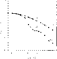
Fig. 3 represents the dewater comparison of removing efficient of efficient and current techniques material therefor and method of the present invention; With
Fig. 4 represents the comparison that removes water stability and current techniques method therefor of the inventive method.
Preferred embodiment is described
Find out the most significantly from Fig. 1, electronic device 100 of the present invention comprises that polymer-electronics device 110, this electrode of being made up of anode 112 and negative electrode 114 have the substrate 122 in attached lead 116,118, electroactive organic polymer layers 120 and the present embodiment.This device 110 also comprises enclosure 124, and it separates electronic device and atmosphere.This enclosure is made substrate by substrate 122, has lid or covers 126, and this cover is fixed on the substrate 122 by bonding agent 128.Drier 130 is enclosed box 124, preferably is fixed on the inner surface 132 of box by bonding agent 134.Substrate
Substrate 122 is normally airtight and not saturating moisture.In a preferred embodiment, substrate is a glass.In second embodiment preferred, substrate is a silicon.In the 3rd preferred embodiment, substrate is a flexible substrate, as contains air-locked plastics or composite material inorganic and the plastic material combination.Effectively the example of flexible substrate comprises the plate or the multilayer layer pressing plate of flexible material, flexible material such as impervious flexiplast such as polyester, polyethylene terephthalate for example, or by plastic plate and deposition optional metal or the composite material formed of inorganic dielectric matter layer on it.In a preferred embodiment, substrate is transparent (or translucent), and it can make light enter encapsulation region the light that will launch is passed from encapsulation region.Enclosure
Level Hermetic Package box 126 separates polymer-electronics device 110 and atmosphere.How pressure-tight box is formed not really important, as long as the process operation does not play illeffects to the assembly of polymer-electronics device 110.For example, pressure-tight box 126 can be by forming with adhesive bonds polylith plate together.In a preferred embodiment, pressure-tight box comprises cover 126 compositions that are bonded on the substrate.Can find out the most significantly that from Fig. 1 preferred substrate 122 is substrates of polymer-electronics device 110.
Being used to form the material of pressure-tight box 126 should be airtight and moisture thoroughly.In one embodiment, cover is made of metal.In another embodiment, cover is made by glass or by ceramic material, also can adopt air proof and fluid-tight plastics.
The thickness of cover 126 is not very important in the present invention, as long as the thickness of cover is enough to form continuous barrier (tight and free of pinholes).The thickness of cover 126 should be between 10-1000 μ m.Not (not shown) under the situation of polymer-electronics device substrate at substrate, can imagine that base can be by making with the cover identical materials.Find out that from Fig. 1 is the most obvious cover 126 is to be sealed on the substrate 122 by bonding agent 128.This bonding agent should solidify under the temperature of the decomposition temperature that is lower than active layer 120, for example below 75 ℃, and should be below 50 ℃, preferably under room temperature or moderate temperature.This is favourable, because it can not run in the common high temperature of prior art, this high temperature often makes electronic device 110 impaired or performance reductions.Preferred bonding agent comprises epoxy resin, and it can solidify under ultraviolet light irradiation or under the moderate temperature of mentioning in the above in (or under two kinds of effects).Find out that from Fig. 1 is the most tangible lead 116,118 stretches out from device.These leads should seal with bonding agent 128 equally, but also can adopt the identical conductor structure of function.Solid drier
Cover 126 be sealed on the substrate 122 and encasing electronic components 110 before, need to insert solid driers (drying material) 130.The shape of drier is unimportant.For example drier can be porous packing powder, compressing tablet, be included in solid in the gel, wrap in the solid in the cross-linked polymer and/or the shape of film.Drier can be placed in the enclosure 124 in every way.For example, drier 130 can be added on the coating of substrate or the inner surface (not shown) of cover, perhaps, obviously sees as Fig. 1, with bonding agent 134 drier 130 is fixed on the inner surface 132 of enclosure 124.(not shown) can be added to drier in the flexible substrate of electronic device in addition or one or more layers of multi layer substrate or laminated substrate among.
The character of solid drier is important.It is a kind of solid of porous, and the most common is the inoganic solids with controllable hole structure, and hydrone can enter pore structure, but hydrone is subjected to Physical Absorption in this structure, seemingly is captured and is not discharged in the environment of enclosure.Molecular sieve is a kind of such material.In a preferred version, the drier that is encapsulated in packing is a zeolite.Zeolite is the material of knowing, and can buy from the market.In general, any zeolite all can be used to capture water.Known zeolites is that the aluminium of almost equivalent of counter ion counterionsl gegenions and the oxide of silicon are formed by sodium.Zeolitic material absorbs moisture by Physical Absorption rather than by chemical reaction.Physical Absorption is preferred.
In a preferred scheme, the drier 130 that is encapsulated into enclosure is that a kind of Tri-Sorb of being called as (is sold by S ü d-Chemie exploitation packaging company, the member of S ü d-Chemie group, branch of United Catalysts, Inc, be positioned at Belen, New Mexico) zeolitic material.The structure of Tri-Sorb is by constituting as the aluminium of the almost equivalent of counter ion counterionsl gegenions and the oxide of silicon with sodium.Tri-Sorb is with the Physical Absorption moisture.When adopting the method encapsulation of the present invention's narration, can from embodiment, find out in the stability of polymer LED and the remarkable improvement of phase in longevity.Particularly, the zeolitic material of the Physical Absorption of packing into is made drier and obviously is better than making drier with barium monoxide, and barium monoxide is with the chemical absorbing moisture.
Dry dosage to be added is captured in its inner moisture when the absorption enclosure sealing of enough capacity should be able to be provided.The water absorption capacity of drier is a kind of known character.Air humidity in the internal volume of device and the enclosure is easy to determine.Change and consider the drier that enough weight can be determined and add afterwards to these factors.
In a preferred version, can add drier above amount of calculation, enter the residual water quantity of steam of active device regions and/or pass the remaining permeability of substrate so that offset by incomplete seamed edge sealing.Active layer
Material likely as active layer 120 in electronic device that the present invention protected such as the polymer LED is that poly-(phenylene vinylidene) is PPV; with the soluble derivative of PPV as poly-(2-methoxyl group-5-(2 '-ethyl-own oxygen base)-1; the 4-phenylene vinylidene) be MEH-PPV, the semi-conducting polymer of a kind of for example energy gap>2.1eV.U.S. Patent No. 5,189,136 have described this material in more detail.The useful in the present invention another kind of material of describing is that poly-(2, two (the cholestane oxygen)-1 of 5-, 4-phenylene vinylidene) are BCHA-PPV, the semi-conducting polymer of a kind of energy gap>2.2eV.This material is these thin U.S. Patent application series No.07/800,555 of being described in more.Other suitable polymer blend comprises, for example, poly-(3-alkylthrophene) and the related derivatives that M.Berggren, O.Inganas, G.Gustafsson, J.Rasmusson, M.R.Anderson, T.Hjertberg and O.Wennerstrom are reported of D.Braun, G.Gustafsson, D.Mc Branch and A.J.Heeger report in J.Appl.Phys. (applicating physical magazine) 72,564 (1992); G.Grem, G.Leditzkg, B.Ullrich and G Lerising are at Adv.Mater, (material in modern age) 4, in 36 (1992) poly-(to the phenylene) of report, with Z.Yang, I.Sokolik, F.E, Karasz is at Macromolecules (macromolecule), its soluble derivative of report in 26,1188 (1993), I.D.Parker is in J.Appl.Phys.Appl.Phys.Lett. (Applied Physics, the Applied Physics communication) poly quinoline of being reported in 65,1272 (1994).The admixture of the conjugation semi-conducting polymer in non-conjugated main polymer also can be used as the active layer of polymer LED, relevant report is seen the Synth.Met. of C.Zhang, H.von Seggem, K.Pakbaz, B.Kraabel, H.W.Schmidt and A.J.Heeger, (synthetic material) 62,35 (1994).The same available admixture that comprises two or more conjugated polymers is about reporting the Synth.Met. (synthetic material) that sees H.Nishino, G.Yu, T-A.Chen, R.D.Rieke and A.J.Heeger, 48 243 (1995).In general, the material that is used as active layer in polymer LED comprises semiconductive conjugated polymer, the semiconductive conjugated polymer of display light photoluminescence more particularly, and more particularly display light photoluminescence and be the semiconductive conjugated polymer that can be converted into uniform film of solubility again from solution.High work function anode
The metal that is used as the suitable higher work function of anode material 112 is transparent conductive film [H.Burroughs, D.D.C.Bradley, A.R.Brown, R.N.Marks, K.Mackay, R.H.Friend, P.L.Burns and the A.B Holmes of indium/tin-oxide, Nature (nature) 347,539 (1990); D.Braun and A.J.Heeger, Appl.Phys.Lett. (Applied Physics communication) 58,1982 (1991)].In addition, the film of conducting polymer also can use, as by G.Gustafsson, Y.Cao, G.M.Treacy, F.Klavetter, N.Colaneri and A.J.Heeger, and Nature (nature), 357,477 (1992); Y.Yang and A.J.Heeger, Appl.Phys.Lett. (Applied Physics communication) 64,1245 (1994) and United States Patent (USP) are by asking sequence No.08/205,519; Y.Yang, E.Westerweele, C.Zhang, P.Smith and A.J.Heeger, J.Appl.Phys. (applicating physical magazine) 77,694 (1995); J.Cao, A.J.Heeger, J.Y.Lee and C.Y.Kim, Synth.Met. (synthetic material) 82,221 (1996) and Y.Cao, G.Yu, C.Zhang, R.Menon and A.J.Heeger, Appl.Phys.Lett, (Applied Physics communication) 70,3191 (1997) confirm.The bilayer anode that contains the polyaniline film of indium/tin-sull and emeraldine salt form is preferred because as transparency electrode, two kinds of materials all can make light from the LED emission with effective level from the device radiation.Low work function negative electrode
It is suitable that what make cathode material 114 is alkaline-earth metal such as calcium, barium, strontium and rare earth metal such as ytterbium than low work function metal.The alloy of low work function metal, for example alloy and lithium the alloy in aluminium of magnesium in silver is (U.S. Patent No. 5,047,687 that prior art is known equally; 5,059,862 and 5,408,109).Electronics injects the thickness of cathode layer at 200-5000 , as (the United States Patent (USP) 5,151 that prior art confirmed, 629,5,247,190,5,317,167 and J.Kido, H.Shionoya, K Nagai, Appl.Phys.Lett. (Applied Physics communication), 67 (1995) 2281).Lower limit 200-500 dust () is to form cathode layer continuous film (all standing) desired (United States Patent (USP) 5,512,654; J.C.Scott, J.H.Kaufman, P.J.Brock, R.DiPietro, J.Salem and J.A.Goitia, J.Appl.Phys. (applicating physical magazine), 79 (1996) 2745; I.D.Parker, H.H.Kim, Appl.Phys.Lett. (Applied Physics communication), 64 (1994) 1774).Except that good covering, think that thicker cathode layer can provide from encapsulation, so that the active component of oxygen and water vapour and device is separated.
The injection electronic cathode of the superthin layer of alkaline including earth metal calcium, strontium and barium is existing report aspect high brightness and high efficiency polymer LED.Compare with the conventional negative electrode of making greater than the same metal (with other low effusion function metal) of 200 by thickness, thickness is less than the superthin layer alkaline-earth metal negative electrode of 100 , than polymer LED tangible improvement (Y.Cao and G.Yu are being arranged aspect stability and useful life, U.S. Patent application 08/872,657).
To high brightness and high efficiency polymer LED are arranged, also reported the injection electronic cathode (PCT such as Y.Cao application No.US99/23775, on October 12nd, 1999 submitted to) of the oxide that contains superthin layer alkaline earth metals calcium, strontium and barium.
The structure and the material therefor and very close that are used for light-sensitive device and device display based on the manufacturing of the LED of polymer.LED and the main difference between the photosensor based on polymer are to use reactive low work function electrode, and the electric polarity of electrode is reverse.But need pack with the long-life light-sensitive device that conducting polymer is made.Therefore, enclosure of the present invention also is useful to these devices, and this encapsulation is enough to prevent that water vapour and oxygen from diffusing into this device, and does not limit its useful life.
The present invention further sets forth with reference to the following examples.These embodiment just illustrate the Implementation Modes that the present invention is different, can not think limitation of the present invention.
Embodiment 1
Drier (Tri-Sorb) based on zeolite is used as drier.Adopt the example of polymer LED (LED) display conduct based on the electronic device of polymer.
The air proof made from glass and the cover of water, it comprises the sheet of being made up of zeolite and (develops packaging company available from S ü d-Chemie, the member of S ü d-Chemie group, branch of United Catalysts, Inc, be positioned at Belen, New Mexico), encapsulate this LED display with it, thereby itself and atmosphere are separated.
Drier is enclosed in the packing, the usefulness heat-curable epoxy resin (Araldite 2014, CibaSpecialty Chemicals company., East Lansing Michigan) is fixed on drier on the inner surface of impervious cover as bonding agent,
Drier is a powder pelleting form.Impervious cover uses bonding agent attached on the substrate.The structure 100 of entire device is shown in Fig. 1.Cover is sealed on the glass substrate as bonding agent with Araldite 2014.
After the package encapsulation, measure the size of light-emitting pixels immediately.Device with packing was placed in 85 ℃ the stove that ambient humidity is arranged with the long time then.With 50 hours be the interval, device is taken out from stove, measure the light-emitting pixels size again.The polymer-electronics device is because the deterioration of moisture and the oxygen effect loss quantification of active region.In this specific embodiment, measure the loss of the luminous zone of pixelation light-emitting diode display.As shown in Figure 2, Tri-Sorb makes the luminous zone loss after storing 300 hours under 85 ℃ be lower than 2%.
Equally, as shown in Figure 2, obviously be better than other example based on the drier (in this specific embodiment, using trade (brand) name Tri-Sorb) of zeolite, as BaO and CaSO
4(it is the efficient drying agent material that this technical field adopted in the past) (the special agent 5,882,761 of the U.S.).Present embodiment shows, based on the drier of zeolite even at high temperature also can become effectively drier.
Present embodiment repeats the experiment of embodiment 1, and difference is to change storage condition, comprises high humidity, i.e. 85 ℃/85% relative humidity.As shown in Figure 3, polymer device emitter region loss 5% after 300 hours.
Also can find out that from Fig. 3 the zeolite system is better than a lot of other drier and comprises BaO and CaO (they are the efficient drying agent materials in the previous patent, United States Patent (USP) 5,882,761).
Present embodiment shows, based on the drier of zeolite even also be effectively drier under high temperature, high humidity environment.
Embodiment 3
Present embodiment repeats the experiment of embodiment 1, and difference is that drier is to be contained in the bag of porous with powder type, and with the inner surface of adhesive securement at impermeable cover.The loss of emitter region and relatively be shown in Fig. 2 and Fig. 3.
This example shows that the concrete physical form of drier is inessential.
Embodiment 4
Present embodiment has carried out the research of the thermogravimetry loss in weight to Tri-Sorb and BaO, to compare its performance that persistence dewaters from the electron device package box.Adopted the thermogravimetric analysis equipment through demarcating of standard.Tri-Sorb and BaO sheet heat (from room temperature to 400 ℃) in dry air, the quality of the sheet of continuous monitoring is not simultaneously found hysteresis.
The results are shown in Fig. 4.At room temperature two samples all absorb moisture.When it was heated, both all disengaged water owing to thermodynamic process, thereby example weight is reduced.But as can be seen, the water that Tri-Sorb disengages is less.Under 85 ℃, the water that the Tri-Sorb sample disengages lacks three times than the BaO sample.
This example shows that at high temperature the hydropexis character of Tri-Sorb is better than BaO (it is as 85 ℃ of special agent of good drier application down by Pioneer).
From top narration as can be seen, the invention provides a kind of technology that is used for encapsulation polymer light-emitting device under minimum possible method temperature.This method for packing helps providing sealing between the surrounding air of device and harmful wet steam and oxygen.In addition, this method for packing is not obviously increased by the device gross thickness that encapsulation brought of device.Once more, this method for packing is less than the method for current known technology by each required operation.
Claims (26)
1. an electronic device (100) comprising:
Polymer-electronics device (110), it comprises pair of electrodes (112,114) opposite one another and places active polymer (120) between two electrodes;
Airtight envelope box (124), it has inner surface (132) adjacent with the polymer-electronics device and the opposed outer surface adjacent with outside atmosphere;
Drier (130), adjacent with inner surface, this drier has a kind of loose structure, and can capture water by Physical Absorption, makes it enter loose structure;
Wherein the level Hermetic Package box is with this polymer-electronics device package, so that this polymer-electronics device and drier and outside atmosphere are separated.
2. method of making long-life electronic device based on organic polymer comprises:
Purchase polymerization electronic device (110), the mutual pair of electrodes facing of this device tool (112,114) and place active polymer (120) between the electrode;
This polymer-electronics device is encapsulated in the level Hermetic Package box (124) with solid drier (130), this drier has loose structure, can capture water by Physical Absorption, and make it enter loose structure, this enclosure separates device and drier and outside atmosphere.
3. the method for the electronic device of claim 1 and/or claim 2, wherein this polymer-electronics device comprises the substrate with at least one substrate layer, solid drier is incorporated among one or more layers of this at least one substrate layer.
4. the method for the electronic device of claim 1 and/or claim 2, wherein drier is a molecular sieve.
5. the method for the electronic device of claim 1 and/or claim 2, wherein drier comprises zeolite.
6. the method for the electronic device of claim 1 and/or claim 2, wherein drier comprises Trisorb.
7. the method for the electronic device of claim 1 and/or claim 2, it is free isolated wherein being present in drier in the enclosure and electrode and polymeric layer.
8. the method for the electronic device of claim 1 and/or claim 2, wherein drier is present on the surface in this level Hermetic Package box.
9. the method for the electronic device of claim 1 and/or claim 2, wherein the polymer-electronics device also comprises the substrate of support polymer layer and electrode, drier is present on the surface of this substrate in the base.
10. the method for the electronic device of claim 1 and/or claim 2, wherein drier is attached on the surface in this level Hermetic Package box
11. the electronic device of claim 1 and/or the method for claim 2, wherein drier is bonded on the interior surface of this level Hermetic Package box.
12. the electronic device of claim 1 and/or the method for claim 2, wherein drier exists with the pelleting form.
13. the electronic device of claim 1 and/or the method for claim 2, wherein drier exists with the powder type that is contained in the porous bag.
14. the electronic device of claim 1 and/or the method for claim 2, wherein drier exists with the solid form that is contained in the porous gel.
15. the electronic device of claim 1 and/or the method for claim 2, wherein drier exists with the solid form that is contained in the film.
16. the electronic device of claim 1 and/or the method for claim 2, wherein drier exists with the solid form that is contained in the bonding agent.
17. the electronic device of claim 1 and/or the method for claim 2, wherein this comprises anode and negative electrode to electrode, and this negative electrode comprises the metal or the metal oxide of the low work function of water reaction.
18. the electronic device of claim 1 and/or the method for claim 2, wherein this comprises anode and negative electrode to electrode, and this negative electrode comprises the alkaline-earth metal or the metal oxide of the low work function of water reaction.
19. the electronic device of claim 1 and/or the method for claim 2, wherein this comprises anode and negative electrode to electrode, and this negative electrode comprises the water reactive explosive that is selected from calcium, barium, strontium, calcium oxide, barium monoxide and strontium oxide strontia.
20. the electronic device of claim 1 and/or the method for claim 2, wherein this polymer-electronics device is a light-emitting diode.
21. the electronic device of claim 1 and/or the method for claim 2, wherein this polymer-electronics device is a light-sensitive detector.
22. the electronic device of claim 1 and/or the method for claim 2, wherein this level Hermetic Package box is made up of the polylith assembly with adhesive bonds.
23. the electronic device of claim 1 and/or the method for claim 2, wherein this bonding agent is a low temperature adhesive.
24. the electronic device of claim 1 and/or the method for claim 2, wherein this low temperature adhesive is an epoxy resin.
25. the electronic device of claim 1 and/or the method for claim 2, wherein this level Hermetic Package box comprises the substrate bonding with cover.
26. the electronic device of claim 1 and/or the method for claim 2, wherein the polymer-electronics device also comprises, the substrate of support polymer layer and electrode, wherein this level Hermetic Package box comprises and the bonding substrate of cover, and with substrate as substrate.
Applications Claiming Priority (2)
| Application Number | Priority Date | Filing Date | Title |
|---|---|---|---|
| US15253699P | 1999-09-03 | 1999-09-03 | |
| US60/152,536 | 1999-09-03 |
Publications (1)
| Publication Number | Publication Date |
|---|---|
| CN1385053A true CN1385053A (en) | 2002-12-11 |
Family
ID=22543345
Family Applications (1)
| Application Number | Title | Priority Date | Filing Date |
|---|---|---|---|
| CN00815087A Pending CN1385053A (en) | 1999-09-03 | 2000-09-01 | Encapsulation of organic electronic devices |
Country Status (7)
| Country | Link |
|---|---|
| EP (1) | EP1208726A1 (en) |
| JP (1) | JP2003508891A (en) |
| KR (1) | KR20020066321A (en) |
| CN (1) | CN1385053A (en) |
| CA (1) | CA2381230A1 (en) |
| TW (1) | TW508970B (en) |
| WO (1) | WO2001019142A1 (en) |
Cited By (3)
| Publication number | Priority date | Publication date | Assignee | Title |
|---|---|---|---|---|
| CN100438120C (en) * | 2003-04-08 | 2008-11-26 | 日本东北先锋公司 | Organic electroluminescent panel and its mfg. method |
| CN102576819A (en) * | 2009-07-31 | 2012-07-11 | 通用电气公司 | Hermetic package with getter materials |
| CN102654282A (en) * | 2011-03-02 | 2012-09-05 | 隆达电子股份有限公司 | Light emitting device with moisture absorption structure |
Families Citing this family (92)
| Publication number | Priority date | Publication date | Assignee | Title |
|---|---|---|---|---|
| JP4526682B2 (en) * | 2000-03-28 | 2010-08-18 | 日東電工株式会社 | Electroluminescence element |
| US7026758B2 (en) * | 2001-09-28 | 2006-04-11 | Osram Opto Semiconductors Gmbh | Reinforcement of glass substrates in flexible devices |
| DE10236855B4 (en) * | 2002-08-07 | 2006-03-16 | Samsung SDI Co., Ltd., Suwon | Housing unit for the encapsulation of components and method for their preparation |
| GB0219223D0 (en) * | 2002-08-17 | 2002-09-25 | Cambridge Display Tech Ltd | Organic optoelectronic device encapsulation package |
| EP1537612B1 (en) | 2002-09-03 | 2010-05-19 | Cambridge Display Technology Limited | Method of forming an optical device |
| US6887733B2 (en) | 2002-09-11 | 2005-05-03 | Osram Opto Semiconductors (Malaysia) Sdn. Bhd | Method of fabricating electronic devices |
| US7224116B2 (en) | 2002-09-11 | 2007-05-29 | Osram Opto Semiconductors Gmbh | Encapsulation of active electronic devices |
| US7193364B2 (en) | 2002-09-12 | 2007-03-20 | Osram Opto Semiconductors (Malaysia) Sdn. Bhd | Encapsulation for organic devices |
| EP1416028A1 (en) | 2002-10-30 | 2004-05-06 | Covion Organic Semiconductors GmbH | New method for the production of monomers useful in the manufacture of semiconductive polymers |
| CN100334718C (en) * | 2002-12-03 | 2007-08-29 | 铼宝科技股份有限公司 | Packaging structure of organic electroluminescent cell and making process thereof |
| GB0306409D0 (en) | 2003-03-20 | 2003-04-23 | Cambridge Display Tech Ltd | Electroluminescent device |
| WO2004106409A1 (en) | 2003-05-30 | 2004-12-09 | Covion Organic Semiconductors Gmbh | Polymer |
| EP1491568A1 (en) | 2003-06-23 | 2004-12-29 | Covion Organic Semiconductors GmbH | Semiconductive Polymers |
| US7135357B2 (en) | 2003-10-06 | 2006-11-14 | E. I. Du Pont De Nemours And Company | Process for making an organic electronic device having a roughened surface heat sink |
| US7438829B2 (en) | 2003-11-13 | 2008-10-21 | E.I. Du Pont De Nemours And Company | Thick film getter paste compositions for use in moisture control |
| GB0329364D0 (en) | 2003-12-19 | 2004-01-21 | Cambridge Display Tech Ltd | Optical device |
| WO2005078458A1 (en) | 2004-02-05 | 2005-08-25 | Analog Devices, Inc. | Capped sensor |
| GB0411582D0 (en) | 2004-05-24 | 2004-06-23 | Cambridge Display Tech Ltd | Metal complex |
| GB0411572D0 (en) | 2004-05-24 | 2004-06-23 | Cambridge Display Tech Ltd | Light-emitting device |
| WO2006016153A1 (en) | 2004-08-10 | 2006-02-16 | Cambridge Display Technology Limited | Light emissive device |
| GB0427266D0 (en) | 2004-12-13 | 2005-01-12 | Cambridge Display Tech Ltd | Phosphorescent OLED |
| US9179518B2 (en) | 2004-12-24 | 2015-11-03 | Cambridge Display Technology Limited | Light emissive device |
| GB0428445D0 (en) | 2004-12-29 | 2005-02-02 | Cambridge Display Tech Ltd | Blue-shifted triarylamine polymer |
| GB2436996B8 (en) | 2004-12-29 | 2013-12-11 | Cambridge Display Tech Ltd | Rigid amines |
| GB0428444D0 (en) | 2004-12-29 | 2005-02-02 | Cambridge Display Tech Ltd | Conductive polymer compositions in opto-electrical devices |
| US7576426B2 (en) | 2005-04-01 | 2009-08-18 | Skyworks Solutions, Inc. | Wafer level package including a device wafer integrated with a passive component |
| GB0507684D0 (en) | 2005-04-15 | 2005-05-25 | Cambridge Display Tech Ltd | Pulsed driven displays |
| GB0514476D0 (en) | 2005-07-14 | 2005-08-17 | Cambridge Display Tech Ltd | Conductive polymer compositions in opto-electrical devices |
| US20070013305A1 (en) | 2005-07-18 | 2007-01-18 | Wang Carl B | Thick film getter paste compositions with pre-hydrated desiccant for use in atmosphere control |
| GB0518968D0 (en) | 2005-09-16 | 2005-10-26 | Cdt Oxford Ltd | Organic light-emitting device |
| GB2432256B (en) | 2005-11-14 | 2009-12-23 | Cambridge Display Tech Ltd | Organic optoelectrical device |
| GB0526185D0 (en) | 2005-12-22 | 2006-02-01 | Cambridge Display Tech Ltd | Electronic device |
| GB2433509A (en) | 2005-12-22 | 2007-06-27 | Cambridge Display Tech Ltd | Arylamine polymer |
| GB0526393D0 (en) | 2005-12-23 | 2006-02-08 | Cdt Oxford Ltd | Light emissive device |
| GB2433833A (en) | 2005-12-28 | 2007-07-04 | Cdt Oxford Ltd | Micro-cavity OLED layer structure with transparent electrode |
| GB2434915A (en) | 2006-02-03 | 2007-08-08 | Cdt Oxford Ltd | Phosphoescent OLED for full colour display |
| GB2440934B (en) | 2006-04-28 | 2009-12-16 | Cdt Oxford Ltd | Opto-electrical polymers and devices |
| US20090263567A1 (en) | 2006-08-01 | 2009-10-22 | Cambridge Display Technology Limited | Methods of Manufacturing Opto-Electrical Devices |
| US7635606B2 (en) | 2006-08-02 | 2009-12-22 | Skyworks Solutions, Inc. | Wafer level package with cavities for active devices |
| GB0617167D0 (en) | 2006-08-31 | 2006-10-11 | Cdt Oxford Ltd | Compounds for use in opto-electrical devices |
| GB0620045D0 (en) | 2006-10-10 | 2006-11-22 | Cdt Oxford Ltd | Otpo-electrical devices and methods of making the same |
| GB2448175B (en) | 2007-04-04 | 2009-07-22 | Cambridge Display Tech Ltd | Thin film transistor |
| GB2454890B (en) | 2007-11-21 | 2010-08-25 | Limited Cambridge Display Technology | Light-emitting device and materials therefor |
| CN101878527B (en) | 2007-11-30 | 2012-09-26 | 斯盖沃克斯瑟路申斯公司 | Wafer level packaging using flip chip mounting |
| GB2455747B (en) | 2007-12-19 | 2011-02-09 | Cambridge Display Tech Ltd | Electronic devices and methods of making the same using solution processing techniques |
| US8900931B2 (en) | 2007-12-26 | 2014-12-02 | Skyworks Solutions, Inc. | In-situ cavity integrated circuit package |
| GB2456788B (en) | 2008-01-23 | 2011-03-09 | Cambridge Display Tech Ltd | White light emitting material |
| GB0803950D0 (en) | 2008-03-03 | 2008-04-09 | Cambridge Display Technology O | Solvent for printing composition |
| GB2458454B (en) | 2008-03-14 | 2011-03-16 | Cambridge Display Tech Ltd | Electronic devices and methods of making the same using solution processing techniques |
| GB2459895B (en) | 2008-05-09 | 2011-04-27 | Cambridge Display Technology Limited | Organic light emissive device |
| GB2462410B (en) | 2008-07-21 | 2011-04-27 | Cambridge Display Tech Ltd | Compositions and methods for manufacturing light-emissive devices |
| GB2462122B (en) | 2008-07-25 | 2013-04-03 | Cambridge Display Tech Ltd | Electroluminescent materials |
| GB2462314B (en) | 2008-08-01 | 2011-03-16 | Cambridge Display Tech Ltd | Organic light-emiting materials and devices |
| GB0814161D0 (en) | 2008-08-01 | 2008-09-10 | Cambridge Display Tech Ltd | Blue-light emitting material |
| GB0814971D0 (en) | 2008-08-15 | 2008-09-24 | Cambridge Display Tech Ltd | Opto-electrical devices and methods of manufacturing the same |
| GB2462688B (en) | 2008-08-22 | 2012-03-07 | Cambridge Display Tech Ltd | Opto-electrical devices and methods of manufacturing the same |
| GB2463040B (en) | 2008-08-28 | 2012-10-31 | Cambridge Display Tech Ltd | Light-emitting material |
| GB2463077B (en) | 2008-09-02 | 2012-11-07 | Sumitomo Chemical Co | Electroluminescent material and device |
| GB0819449D0 (en) | 2008-10-23 | 2008-12-03 | Cambridge Display Tech Ltd | Display drivers |
| EP2192636A1 (en) | 2008-11-26 | 2010-06-02 | Rijksuniversiteit Groningen | Modulatable light-emitting diode |
| GB2466842B (en) | 2009-01-12 | 2011-10-26 | Cambridge Display Tech Ltd | Interlayer formulation for flat films |
| GB2466843A (en) | 2009-01-12 | 2010-07-14 | Cambridge Display Tech Ltd | Interlayer formulation for flat films |
| GB2469500B (en) | 2009-04-16 | 2012-06-06 | Cambridge Display Tech Ltd | Method of forming a polymer |
| GB2469498B (en) | 2009-04-16 | 2012-03-07 | Cambridge Display Tech Ltd | Polymer and polymerisation method |
| GB0906554D0 (en) | 2009-04-16 | 2009-05-20 | Cambridge Display Tech Ltd | Organic electroluminescent device |
| GB2469497B (en) | 2009-04-16 | 2012-04-11 | Cambridge Display Tech Ltd | Polymers comprising fluorene derivative repeat units and their preparation |
| GB2475246B (en) | 2009-11-10 | 2012-02-29 | Cambridge Display Tech Ltd | Organic opto-electronic device and method |
| GB2475247B (en) | 2009-11-10 | 2012-06-13 | Cambridge Display Tech Ltd | Organic optoelectronic device and method |
| GB2480323A (en) | 2010-05-14 | 2011-11-16 | Cambridge Display Tech Ltd | OLED hole transport layer |
| GB2487342B (en) | 2010-05-14 | 2013-06-19 | Cambridge Display Tech Ltd | Host polymer comprising conjugated repeat units and non-conjugated repeat units for light-emitting compositions, and organic light-emitting devices |
| GB2484253B (en) | 2010-05-14 | 2013-09-11 | Cambridge Display Tech Ltd | Organic light-emitting composition and device |
| DE112011102126T5 (en) | 2010-06-25 | 2013-05-08 | Cambridge Display Technology Limited | Organic light-emitting composition, device and method |
| GB2499969A (en) | 2010-06-25 | 2013-09-11 | Cambridge Display Tech Ltd | Composition comprising an organic semiconducting material and a triplet-accepting material |
| GB2483269A (en) | 2010-09-02 | 2012-03-07 | Cambridge Display Tech Ltd | Organic Electroluminescent Device containing Fluorinated Compounds |
| GB2484537A (en) | 2010-10-15 | 2012-04-18 | Cambridge Display Tech Ltd | Light-emitting composition |
| GB2485001A (en) | 2010-10-19 | 2012-05-02 | Cambridge Display Tech Ltd | OLEDs |
| CN103339167B (en) | 2011-01-31 | 2018-01-12 | 剑桥显示技术有限公司 | Polymer |
| GB2494096B (en) | 2011-01-31 | 2013-12-18 | Cambridge Display Tech Ltd | Polymer |
| GB201105582D0 (en) | 2011-04-01 | 2011-05-18 | Cambridge Display Tech Ltd | Organic light-emitting device and method |
| GB201107905D0 (en) | 2011-05-12 | 2011-06-22 | Cambridge Display Tech Ltd | Light-emitting material, composition and device |
| GB201110565D0 (en) | 2011-06-22 | 2011-08-03 | Cambridge Display Tech Ltd | Organic optoelectronic material, device and method |
| WO2013005028A1 (en) | 2011-07-04 | 2013-01-10 | Cambridge Display Technology Limited | Organic light emitting device and fabrication method thereof |
| GB201111738D0 (en) | 2011-07-08 | 2011-08-24 | Cambridge Display Tech Ltd | Display drivers |
| GB201111742D0 (en) | 2011-07-08 | 2011-08-24 | Cambridge Display Tech Ltd | Solution |
| GB201210131D0 (en) | 2011-11-02 | 2012-07-25 | Cambridge Display Tech Ltd | Light emitting composition and device |
| GB201118997D0 (en) | 2011-11-03 | 2011-12-14 | Cambridge Display Tech Ltd | Electronic device and method |
| JP6225120B2 (en) | 2012-01-31 | 2017-11-01 | ケンブリッジ ディスプレイ テクノロジー リミテッド | polymer |
| GB2505893A (en) | 2012-09-13 | 2014-03-19 | Cambridge Display Tech Ltd | Compounds for use in organic optoelectronic devices |
| CN104910366B (en) * | 2015-05-19 | 2017-04-19 | 浙江理工大学 | Organic quicklime composite desiccant and preparation method therefor |
| US10222256B2 (en) | 2016-09-22 | 2019-03-05 | Apple Inc. | Ambient light sensor system having light-scattering desiccant |
| GB2575089A (en) | 2018-06-28 | 2020-01-01 | Sumitomo Chemical Co | Phosphorescent light-emitting compound |
| JP2021170434A (en) * | 2020-04-14 | 2021-10-28 | 双葉電子工業株式会社 | Organic EL device |
Family Cites Families (9)
| Publication number | Priority date | Publication date | Assignee | Title |
|---|---|---|---|---|
| GB2049274B (en) * | 1979-03-16 | 1983-04-27 | Sharp Kk | Moisture absorptive arrangement for a glass sealed thinfilm electroluminescent display panel |
| IL80861A0 (en) * | 1986-12-03 | 1987-03-31 | Technoset Ltd | Electroluminescent lighting elements |
| US4882518A (en) * | 1988-05-25 | 1989-11-21 | The Cherry Corporation | Back cap for an electroluminescent display |
| JPH04267096A (en) * | 1991-02-21 | 1992-09-22 | Sharp Corp | Thin film electroluminescence panel |
| JPH06176867A (en) * | 1992-12-10 | 1994-06-24 | Denki Kagaku Kogyo Kk | Electroluminescent element |
| WO1996008122A1 (en) * | 1994-09-08 | 1996-03-14 | Idemitsu Kosan Co., Ltd. | Method for sealing organic el element and organic el element |
| KR100500078B1 (en) * | 1996-02-26 | 2005-07-18 | 이데미쓰 고산 가부시키가이샤 | Organic electroluminescent element and method for manufacturing the same |
| JP3899566B2 (en) * | 1996-11-25 | 2007-03-28 | セイコーエプソン株式会社 | Manufacturing method of organic EL display device |
| JPH10275679A (en) * | 1997-03-31 | 1998-10-13 | Toyota Central Res & Dev Lab Inc | Organic el element |
-
2000
- 2000-09-01 EP EP00957945A patent/EP1208726A1/en not_active Withdrawn
- 2000-09-01 KR KR1020027002839A patent/KR20020066321A/en not_active Application Discontinuation
- 2000-09-01 JP JP2001522203A patent/JP2003508891A/en active Pending
- 2000-09-01 CN CN00815087A patent/CN1385053A/en active Pending
- 2000-09-01 WO PCT/US2000/024126 patent/WO2001019142A1/en not_active Application Discontinuation
- 2000-09-01 CA CA002381230A patent/CA2381230A1/en not_active Abandoned
- 2000-09-15 TW TW089117977A patent/TW508970B/en not_active IP Right Cessation
Cited By (3)
| Publication number | Priority date | Publication date | Assignee | Title |
|---|---|---|---|---|
| CN100438120C (en) * | 2003-04-08 | 2008-11-26 | 日本东北先锋公司 | Organic electroluminescent panel and its mfg. method |
| CN102576819A (en) * | 2009-07-31 | 2012-07-11 | 通用电气公司 | Hermetic package with getter materials |
| CN102654282A (en) * | 2011-03-02 | 2012-09-05 | 隆达电子股份有限公司 | Light emitting device with moisture absorption structure |
Also Published As
| Publication number | Publication date |
|---|---|
| WO2001019142A1 (en) | 2001-03-15 |
| KR20020066321A (en) | 2002-08-14 |
| CA2381230A1 (en) | 2001-03-15 |
| JP2003508891A (en) | 2003-03-04 |
| EP1208726A1 (en) | 2002-05-29 |
| TW508970B (en) | 2002-11-01 |
Similar Documents
| Publication | Publication Date | Title |
|---|---|---|
| CN1385053A (en) | Encapsulation of organic electronic devices | |
| KR100635429B1 (en) | Encapsulation of Polymer-Based Solid State Devices with Inorganic Materials | |
| KR101245745B1 (en) | Desiccant sealing arrangement for OLED devices | |
| TW493359B (en) | Plastic substrates with improved barrier properties for devices sensitive to water and/or oxygen, such as organic electroluminescent devices | |
| CN101128074A (en) | An organic EL part and its making method | |
| EP1196955A1 (en) | Long-lifetime polymer light-emitting devices with improved luminous efficiency and radiance | |
| CN102484079A (en) | Encapsulation process and structure for electronic devices | |
| JP4752087B2 (en) | Electroluminescent device | |
| US20030137061A1 (en) | Encapsulation of organic polymer electronic devices | |
| WO2005004547A1 (en) | Light emitting element and display device | |
| KR20010067868A (en) | Organic Light-Emitting Device excellent in endurance and the method of manufacturing the same | |
| JP4272819B2 (en) | Organic light emitting device | |
| JP2007287613A (en) | Organic electroluminescence element and its manufacturing method | |
| WO1999003122A1 (en) | Anhydrous method of packaging organic light emitting displays | |
| WO2017130955A1 (en) | Organic electroluminescent element | |
| JP3695190B2 (en) | Organic EL device and manufacturing method thereof | |
| WO2010131171A2 (en) | Short circuit prevention in electroluminescent devices | |
| WO2004017441A1 (en) | Organic optoelectronic device encapsulation package | |
| JPS61131394A (en) | Manufacture of dispersion type el | |
| CN116615048A (en) | Luminous screen body and preparation method thereof | |
| KR19990084223A (en) | The encapsulated organic light emitting device | |
| KR19990031397A (en) | Manufacturing method of LED type green organic electroluminescent device | |
| JP2004319245A (en) | Organic el panel and its method of manufacture |
Legal Events
| Date | Code | Title | Description |
|---|---|---|---|
| C10 | Entry into substantive examination | ||
| SE01 | Entry into force of request for substantive examination | ||
| C06 | Publication | ||
| PB01 | Publication | ||
| C10 | Entry into substantive examination | ||
| SE01 | Entry into force of request for substantive examination | ||
| C02 | Deemed withdrawal of patent application after publication (patent law 2001) | ||
| WD01 | Invention patent application deemed withdrawn after publication | ||
| REG | Reference to a national code |
Ref country code: HK Ref legal event code: WD Ref document number: 1052272 Country of ref document: HK |