CN1319373C - Method of signal mode identification and setting method of ADC parameter - Google Patents
Method of signal mode identification and setting method of ADC parameter Download PDFInfo
- Publication number
- CN1319373C CN1319373C CNB031358624A CN03135862A CN1319373C CN 1319373 C CN1319373 C CN 1319373C CN B031358624 A CNB031358624 A CN B031358624A CN 03135862 A CN03135862 A CN 03135862A CN 1319373 C CN1319373 C CN 1319373C
- Authority
- CN
- China
- Prior art keywords
- signal
- pattern
- htotal
- value
- vtotal
- Prior art date
- Legal status (The legal status is an assumption and is not a legal conclusion. Google has not performed a legal analysis and makes no representation as to the accuracy of the status listed.)
- Expired - Fee Related
Links
Images

Abstract
The present invention discloses a method for identifying signal patterns and a method for setting ADC parameters, which is characterized in that a signal pattern table is built, and then the signal pattern table is orderly searched according to parameters of a key pattern of input image signals so as to quickly and accurately identify a signal pattern. After an analog image signal pattern is identified, the frequency dividing ratio of pixel clock GCLK, PLL is corrected again according to HTOTAL in ADC digital-analog conversion, so that the ADC digital-analog conversion much accords with actual signals. The present invention can be widely used for liquid crystal products, PDP, HDTV and other digital flat panel displays requiring automatic pattern identification for various analog signal input and digital signals input.
Description
Technical field
The present invention relates to a kind of method of signal mode identification and the method to set up of ADC parameter, particularly relate to a kind of method of image display signal pattern recognition, reach for the simulated image shows signal after pattern recognition is come out the method to set up of ADC parameter.
Technical background
After a kind of new signal was input to the digital imagery treatment system, its signal mode was unknown with vertical resolution to whole digital imagery treatment system as level, but will correctly shows this picture intelligence, just must its signal mode of identification.Present way generally is to start with from row/field sync signal, calculate some parameters of picture intelligence pattern, parameter with these parameters and industry universal standard defined compares one by one again, fit like a glove if having, just as correct signal mode, fit like a glove if can not find, just set an approximate signal pattern commonly used.Mainly there are two problems in such recognition methods: the one, compare one by one, and speed is slow, and recognition time is long; The 2nd, approximate signal pattern commonly used of artificial setting, visual display quality just is difficult to guarantee.
For the simulated image shows signal, common in the past way is after pattern finds, and finds corresponding ADC parameter value that the ADC chip is provided with the way of question blank.The theoretical foundation of this method is that all simulated image shows signal must be in strict accordance with industry standard.But the not enough standard of signal of a lot of low-grade video cards outputs is often arranged in reality,, will cause problems such as visual display effect is not good if blindly apply mechanically the ADC parameter.
Summary of the invention
Purpose of the present invention just provides a kind of method of signal mode identification and the method to set up of ADC parameter, and it can identify the pattern of picture intelligence rapidly and exactly, and according to this pattern proper A DC parameter is set automatically, thereby shows good image quality.
The present invention is achieved in that it may further comprise the steps:
According to the standard of shows signal, set up the pattern list of various shows signal, include V parameter TOTAL, HPER, HTOTAL, VRES, interlaced/progressive in this pattern list; And by interlacing, be separated into two class tables line by line;
To the row/field sync signal of input, OK/the decoding computing of field synchronization, obtain the parameters in the described pattern list;
If parameter is interlacing, with regard to corresponding interlaced mode table, if parameter is for line by line, with regard to correspondence pattern list line by line;
Separately the pattern list of two class shows signal after the correspondence is that key value sorts with the major parameter that calculates again, finds the pattern list of the shows signal of a coupling, thereby determines the pattern of this signal.
After signal mode identifies, if this signal is an analog signal, need carry out the ADC digital-to-analogue conversion, the setting of its ADC parameter realizes according to the following steps:
Calculate pixel clock GCLK according to the HTOTAL value in the pattern;
Calculate the PLL frequency dividing ratio according to pixel clock GCLK again.
Because to adopt major parameter is that key value carries out sorted search in the present invention, so speed is just than comparatively fast, and recognition time will shorten, and if run into the situation that all parameters not fit like a glove, owing to major parameter is arranged as key value, therefore just relatively accurate.Simultaneously pixel clock GCLK, PLL frequency dividing ratio were revised again according to HTOTAL, so ADC digital-to-analogue conversion more realistic signal just, and the tolerance to nonstandard signal will improve like this, and therefore the image quality that shows is just relatively good.
The present invention will be further described in detail below in conjunction with the drawings and specific embodiments.
Description of drawings
Fig. 1 is the block diagram of digital imagery front-end processing system;
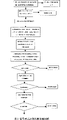
Fig. 2 is the algorithm flow chart of the signal mode identification of present embodiment;
Fig. 3 is the schematic diagram that mode detection and input signal are caught;
Fig. 4 is the schematic diagram of out of phase to the image quality influence.
Embodiment
Be provided with as follows for the picture intelligence pattern list:
● MODE INDEX (BYTE): the index sequence number that forms pattern list;
● HPER (WORD): represent line frequency;
● VTOTAL (WORD): represent every row total synchronously, can calculate field frequency with HPER;
● HTOTAL (WORD): the sum of all pixels of each row;
● HRES (WORD): the sum of all pixels in each line activating interval;
● VRES (WORD): the row in each field activation interval is sum synchronously;
● VDS (WORD): the start of line position in each field activation interval;
● HDS (WORD): the pixel original position in each line activating interval;
● PRFLAG (BYTE): handle sign automatically;
I.INTERLACED (BIT): whether interlacing of input signal;
Ii.HPOLARITY (BIT): the capable synchronous polarity of input signal;
Iii.V POLARITY (BIT): input signal field synchronization polarity;
Iv.COMP SYNC (BIT): whether input signal is the composite sync input;
V.DOS MODE (BIT): whether input signal does not need to do in the future the position adjustment;
Vi.SKIP ALTERNATE H TOTAL (BIT): whether input signal has very close pattern;
● MODE NAME (STRING): MODE name;
The content of pattern list can define according to the Monitor Timing Specifications of VESA.
The number of pattern list is by respectively having 32 with interlacing line by line.
In LCD, PDP, HDTV system, the block diagram of general digital imagery front-end processing system is a digital signal as if input signal as shown in Figure 1 certainly, and the ADC digital-to-analogue conversion has not just needed so, can directly enter image processing GRAPHICS PROCECCER chip.
As Fig. 2, the pattern for correct identification input signal is provided with capable field synchronization interrupt handling routine earlier, by the detection repeatedly of several field signals, confirms to obtain final stable every parameter value that needs, and this need start with from HSYNC and VSYNC signal.For the synchronizing signal of compound input, what at first will do is separated in synchronization.For the row/field sync signal of separating input, need the sync decoder of row/field.The essence of this decoder is exactly counter, counts according to row/field system chronizing impulse.Secondly, the polarity determining device that also needs row/field synchronization.
● during each field synchronization, trigger the counter of horizontal synchronizing pulse, and the result is stored in the register, can obtain the value of VTOTAL; (this register upgraded with the field duration)
● according to system clock UCLK, calculate the clock cycle of being expert at, and the result is stored in the register, can obtain the value of HPER; (this register upgrades with line period)
● according to field sync signal, judge this signal for line by line or interlace signal (INTERLACE);
According to field sync signal, judge field synchronization polarity (VPOL);
● according to line synchronizing signal, judge trip synchronous polarity (HPOL);
If exceed the time restriction of detection, signal or circuit existing problems are described, declaration detects failure, returns.
Then, check whether VTOTAL, HPER, HPOL, VPOL, INTERLACE be legal, if illegal, signal or circuit existing problems be described, and declaration detects fails, and returns.
According to above-mentioned detected value, can calculate the line frequency and the field frequency of input signal, the automatic signal pattern just can correctly be discerned by the mode of query pattern table.In most of the cases, above-mentioned Rule of judgment can find the most close a kind of pattern uniquely in pattern list.If after having inquired about pattern list, found more than the pattern more than 1, that is to say, had some signal and input signal extremely close, their row, field synchronization frequency and polarity are all identical, depend merely on top Rule of judgment and also are not enough to correctly discern input signal pattern.Just need check the value of VRES for further finding correct pattern this moment.
As shown in Figure 3, active images are not just to begin from row field sync signal firm end, can set a threshold value, when detected input data of image processing ics during greater than this threshold value, just think the pictorial data that has found the zone of action.By detection to a field signal, on the horizontal direction from horizontal synchronizing pulse, be made as the horizontal original position (HDS) of zone of action to detected first width value greater than the thresholding pixel, on the vertical direction from field system chronizing impulse, be made as the vertical original position (VDS) of zone of action to detected first capable synchronous number greater than threshold value, in like manner also can obtain HBI (after equaling on the horizontal direction zone of action and finishing, from first less than the pixel location of thresholding to next line first greater than the pixel width value the thresholding pixel location) and VBI (equal after finish the zone of action on the vertical direction, from first row less than thresholding be synchronized to next first greater than the capable capable synchronous number between synchronously of thresholding).
For the simulated image shows signal, because the PLL parameter of ADC chip also is not provided with correctly, this moment, the HDS and the HBI data that obtain were full of prunes, but VDS and VBI be no matter how the parameter of ADC is provided with, and that obtain all is real result.The value of the VRES that obtains according to this (equal VTOTAL and deduct VBI) also is believable.
In order to find new pattern rapidly, save hunting time, just pattern list need be sorted.
At first, be interlacing or line by line scan separately, if parameter is interlacing, with regard to corresponding interlaced mode table, if parameter is for line by line, with regard to correspondence pattern list line by line according to the input signal field synchronization.
Two tables separately are that key value carries out the ordering first time by VTOTAL again, head from the merotype table, seek first and be equal to, or greater than the index of articles number that needs search signal pattern VTOTAL, take this as the standard the pattern query table that 16 patterns that make progress and 15 downward patterns form 32 records.
At this moment, can be according to the value of HPOL and VPOL, from 32 pattern query tables, remove incongruent record, further dwindle query context, with the pattern list of the shows signal that finds a coupling fast.
Certainly, following judgment rule can be utilized, the pattern list of the shows signal of a coupling can be found faster, more accurately.That is: MIN{|modetable[i] .vtotal-newmode.vtotal|+|modetable[i] .hper-newmode.hper|/2}, wherein the weight of VTOTAL is greater than HPER
At this moment, if the ordering second time is carried out with HPER again in pattern quantity>1 of finding, find the pattern list of the shows signal of a coupling.
At this moment, if sort for the third time with VRES again in pattern quantity>1 of finding, find the pattern list of the shows signal of a coupling.
If, still found more than the pattern more than 1 through above-mentioned steps, that is to say have some signal and input signal extremely close, their row, field synchronization frequency and polarity are all identical, and the resolution of vertical direction is all just the same.Run into this situation, can have two kinds of ways to solve:
I. according to some signal mode degree commonly used in actual use, in pattern list, the most frequently used pattern is come the foremost of this several modes, if can not be according to the final pattern of above-mentioned steps assertive signal, the parameter of directly quoting most common patterns be as final result.Certainly, this way has individual shortcoming, might mistake be set pattern exactly when the signal that some utmost point of input is of little use.
If ii. the pattern according to signal is provided with correctly, the hypothesis that visual final mass is all right is checked and rated best match pattern from the angle of image quality.For this processing, just require image processing ics that image quality is had the standards of measurement of carrying out.At the forward pattern of several orderings, establish successively into corresponding ADC register parameters according to pattern list, then after having established parameter each time, all moving an automatic phase detects, obtain the image quality value of feedback PHASEQ of different mode when optimal display result respectively, final relatively these several image quality values of feedback, wherein the pattern of Zui Da value of feedback correspondence is exactly the pattern of mating most.As Fig. 4, image processing ics is a reading of data when the COLCK rising edge, if the phase place that is provided with is inaccurate, and will be at the CLOCK rising edge invalid data that reads back.To same images, PHASEQ equals in the field pattern picture signals, and the visual DATA that the CLOCK rising edge reads is 1 pixel summation.PHASEQ is big more, shows the CLOCK of image and DATA to must be neat more, and the effect of image output is just good more.The benefit of this way is that pattern recognition is more accurate, can obtain the good display effect of image;
After signal mode identified, HTOTAL value wherein used the HTOTAL actual value that numeration obtains from input signal HSYNC horizontal synchronizing pulse to proofread and correct.Like this, even for nonstandard signal, the HTOTAL value in the pattern list also can calibration accuracy.
After the pattern recognition of signal is come out, if this signal is an analog signal, need carry out the ADC digital-to-analogue conversion, the method to set up of its ADC parameter is as follows:
The mode of operation of ADC chip PLL is: with the HSYNC signal Synchronization of importing, according to the pattern that finally finds frequency dividing ratio is set again earlier.After pattern found, HTOTAL had just decided, and the pixel clock GCLK that needs also can correspondingly calculate.
GCLK=mode[modei].Htotal*mode[modei].Vtotal*Vsync;
Can release the parameter of ADC thus:
PLL frequency dividing ratio most-significant byte: PLLDIVH=((mode[modei] .HTotal-1)>>4) ﹠amp; Oxff;
PLL frequency dividing ratio least-significant byte: PLLDILH=((mode[modei] .HTotal-1) ﹠amp; OxOf)<<4).
Claims (9)
1. the method for a signal mode identification is characterized in that comprising the steps:
According to the standard of shows signal, set up the pattern list of various shows signal, include V parameter TOTAL, HPER, HTOTAL, VRES, interlaced/progressive in this pattern list, and by interlacing, be separated into two class tables line by line;
To the row/field sync signal of input, OK/the decoding computing of field synchronization, obtain the parameters in the described pattern list;
If parameter is interlacing, with regard to corresponding interlaced mode table, if parameter is for line by line, with regard to correspondence pattern list line by line;
The pattern list of two class shows signal after the correspondence separately, the major parameter to calculate sorts as key value with major parameter again, finds the pattern list of the shows signal of a coupling, thereby determines the pattern of this signal;
Described major parameter is VTOTAL;
Described VTOTAL is meant in field sync period, the sum that row is synchronous; Described HPER is meant within a certain period of time, the synchronous cycle of experiencing of row; Described HTOTAL was meant in the synchronizing cycle of being expert at, the sum of pixel; Described VRES is meant that in adjacent two field sync signals the row of activation interval is sum synchronously.
2. the method for a kind of signal mode identification according to claim 1, it is characterized in that by after the described VTOTAL key value ordering, value according to HPOL and VPOL, from the pattern query table, remove incongruent record, further dwindle query context, with the pattern list of the shows signal that finds a coupling fast;
Described HPOL is meant the capable synchronous polarity of input signal; Described VPOL is meant input signal field synchronization polarity.
3. the method for a kind of signal mode identification according to claim 2, after it is characterized in that removing incongruent record by described method, according to following judgment rule, find the pattern list of the shows signal of a coupling, that is: MIN{|modetable[i] .vtotal-newmode.vtotal|+|modetable[i] .hper-newmode.hper|/2}, wherein the weight of VTOTAL is greater than HPER.
4. according to the method for claim 1 or 2 or 3 described a kind of signal modes identifications, it is characterized in that carry out the ordering first time as key value with described VTOTAL after, identical VTOTAL carries out the ordering second time by HPER, find the pattern list of the shows signal of a coupling, thereby determine the pattern of this signal.
5. the method for a kind of signal mode identification according to claim 4, it is characterized in that carrying out after the second time ordering as key value with described HPER, identical HPER sorts for the third time by HTOTAL, find the pattern list of a shows signal of mating most, thereby determine the pattern of this signal.
6. the method for a kind of signal mode identification according to claim 5, after it is characterized in that sorting for the third time as key value with described HTOTAL, identical HTOTAL carries out the 4th minor sort by VRES, find the pattern list of a shows signal of mating most, thereby determine the pattern of this signal.
7. according to the method for the identification of a kind of signal mode described in the claim 6, it is characterized in that if this signal is for need carry out the analog-to-digital analog signal of ADC, then in the forward pattern of ordering, establish successively into corresponding ADC register parameters according to pattern list, then after having established parameter each time, all moving an automatic phase detects, obtain the image quality value of feedback PHASEQ of different mode when optimal display result respectively, to same images, PHASEQ equals in the field pattern picture signals, and the visual DATA that the CLOCK rising edge reads is 1 pixel summation, and PHASEQ is big more, show the CLOCK of image and DATA to must be neat more, the effect of image output is just good more; Final relatively these several image quality value of feedback PHASEQ, wherein the pattern of Zui Da value of feedback correspondence is exactly the pattern of mating most.
8. according to the method for claim 1,2,3,5,6 or 7 described a kind of signal modes identifications, it is characterized in that, after signal mode identified, HTOTAL value wherein used the HTOTAL actual value that numeration obtains from input signal HSYNC horizontal synchronizing pulse to proofread and correct.
9. the method for a kind of signal mode identification according to claim 4 is characterized in that after signal mode identified, HTOTAL value wherein used the HTOTAL actual value that numeration obtains from input signal HSYNC horizontal synchronizing pulse to proofread and correct.
Priority Applications (1)
| Application Number | Priority Date | Filing Date | Title |
|---|---|---|---|
| CNB031358624A CN1319373C (en) | 2003-09-19 | 2003-09-19 | Method of signal mode identification and setting method of ADC parameter |
Applications Claiming Priority (1)
| Application Number | Priority Date | Filing Date | Title |
|---|---|---|---|
| CNB031358624A CN1319373C (en) | 2003-09-19 | 2003-09-19 | Method of signal mode identification and setting method of ADC parameter |
Publications (2)
| Publication Number | Publication Date |
|---|---|
| CN1538747A CN1538747A (en) | 2004-10-20 |
| CN1319373C true CN1319373C (en) | 2007-05-30 |
Family
ID=34323198
Family Applications (1)
| Application Number | Title | Priority Date | Filing Date |
|---|---|---|---|
| CNB031358624A Expired - Fee Related CN1319373C (en) | 2003-09-19 | 2003-09-19 | Method of signal mode identification and setting method of ADC parameter |
Country Status (1)
| Country | Link |
|---|---|
| CN (1) | CN1319373C (en) |
Families Citing this family (2)
| Publication number | Priority date | Publication date | Assignee | Title |
|---|---|---|---|---|
| CN102956177B (en) * | 2011-08-22 | 2015-09-30 | 冠捷投资有限公司 | The method preventing display screen picture fuzzy and display screen |
| CN104112418B (en) * | 2013-04-18 | 2016-12-28 | 冠捷投资有限公司 | The method identifying analog video signal |
Citations (4)
| Publication number | Priority date | Publication date | Assignee | Title |
|---|---|---|---|---|
| CN87101244A (en) * | 1986-11-20 | 1988-07-20 | 英国电讯公司 | Mode treatment |
| CN1246022A (en) * | 1998-08-20 | 2000-03-01 | 三星电子株式会社 | Video format pattern detector |
| CN1375815A (en) * | 2001-03-20 | 2002-10-23 | 三星电子株式会社 | Method and systme for automatically setting display mode of display device, and recording medium thereof |
| CN1411273A (en) * | 2001-09-29 | 2003-04-16 | 三星电子株式会社 | Apparatus and method for detecting display mode |
-
2003
- 2003-09-19 CN CNB031358624A patent/CN1319373C/en not_active Expired - Fee Related
Patent Citations (4)
| Publication number | Priority date | Publication date | Assignee | Title |
|---|---|---|---|---|
| CN87101244A (en) * | 1986-11-20 | 1988-07-20 | 英国电讯公司 | Mode treatment |
| CN1246022A (en) * | 1998-08-20 | 2000-03-01 | 三星电子株式会社 | Video format pattern detector |
| CN1375815A (en) * | 2001-03-20 | 2002-10-23 | 三星电子株式会社 | Method and systme for automatically setting display mode of display device, and recording medium thereof |
| CN1411273A (en) * | 2001-09-29 | 2003-04-16 | 三星电子株式会社 | Apparatus and method for detecting display mode |
Also Published As
| Publication number | Publication date |
|---|---|
| CN1538747A (en) | 2004-10-20 |
Similar Documents
| Publication | Publication Date | Title |
|---|---|---|
| US6999092B2 (en) | Image display apparatus in which a specific area display attribute is modifiable | |
| CN1190957C (en) | Apparatus and method for detecting display mode | |
| EP0918313A1 (en) | Signal processing method for an analogue picture signal | |
| US8704805B2 (en) | System and method for handling image data transfer in a display driver | |
| US7224340B2 (en) | Method of processing signal of LCM timing controller | |
| CA1233244A (en) | Digital video sync detection | |
| US6559837B1 (en) | Image luminance detection and correction employing histograms | |
| CN103024430B (en) | Control display method and system for simulating red, green and blue (RGB) signal | |
| CN1319373C (en) | Method of signal mode identification and setting method of ADC parameter | |
| US5121440A (en) | Analog video character recognition system | |
| CN109618074B (en) | Robustness design method for nonstandard input vesa time sequence | |
| KR20040018930A (en) | Regenerator circuit of serial data and method regenerating same | |
| WO2005125191A1 (en) | Video format detector and integrated circuit comprising such video format detector as well as method for distinguishing different standards and/or types of video formats | |
| US5608461A (en) | Programmable video frame detector | |
| JP3290744B2 (en) | Control method of CRT display device | |
| US8203651B2 (en) | Video signal synchronization | |
| US5341217A (en) | Digital adaptive video synchronizer | |
| KR20160047678A (en) | Data enable signal generation method, timing controller, and display device | |
| US7705917B2 (en) | Method and circuit for extracting synchronization signals in a video signal | |
| CN100428205C (en) | Method for determining digital image signal of digital display | |
| JP3116677B2 (en) | HDTV signal level determination circuit | |
| CN1084339A (en) | Have the television line of good noise immunity and the checkout gear of field | |
| JP3397813B2 (en) | Display device having input video signal discrimination function | |
| US20050195176A1 (en) | Apparatus and method for processing synch signals in graphic controllers | |
| JP3291330B2 (en) | Character display device and microcomputer provided therewith |
Legal Events
| Date | Code | Title | Description |
|---|---|---|---|
| C06 | Publication | ||
| PB01 | Publication | ||
| C10 | Entry into substantive examination | ||
| SE01 | Entry into force of request for substantive examination | ||
| C14 | Grant of patent or utility model | ||
| GR01 | Patent grant | ||
| CF01 | Termination of patent right due to non-payment of annual fee |
Granted publication date: 20070530 Termination date: 20180919 |
|
| CF01 | Termination of patent right due to non-payment of annual fee |