CN1286145C - Substrate linkage using selenylation reaction - Google Patents
Substrate linkage using selenylation reaction Download PDFInfo
- Publication number
- CN1286145C CN1286145C CNB021032106A CN02103210A CN1286145C CN 1286145 C CN1286145 C CN 1286145C CN B021032106 A CNB021032106 A CN B021032106A CN 02103210 A CN02103210 A CN 02103210A CN 1286145 C CN1286145 C CN 1286145C
- Authority
- CN
- China
- Prior art keywords
- substrate
- active
- bonding
- base substrate
- layer
- Prior art date
- Legal status (The legal status is an assumption and is not a legal conclusion. Google has not performed a legal analysis and makes no representation as to the accuracy of the status listed.)
- Expired - Fee Related
Links
- 239000000758 substrate Substances 0.000 title claims abstract description 335
- 238000006243 chemical reaction Methods 0.000 title abstract description 22
- 239000000463 material Substances 0.000 claims abstract description 171
- 150000001875 compounds Chemical class 0.000 claims abstract description 105
- 239000011669 selenium Substances 0.000 claims abstract description 56
- 238000000034 method Methods 0.000 claims abstract description 32
- 229910052714 tellurium Inorganic materials 0.000 claims abstract description 30
- 238000000137 annealing Methods 0.000 claims abstract description 24
- BUGBHKTXTAQXES-UHFFFAOYSA-N Selenium Chemical compound [Se] BUGBHKTXTAQXES-UHFFFAOYSA-N 0.000 claims abstract description 22
- APFVFJFRJDLVQX-UHFFFAOYSA-N indium atom Chemical compound [In] APFVFJFRJDLVQX-UHFFFAOYSA-N 0.000 claims abstract description 22
- 229910052711 selenium Inorganic materials 0.000 claims abstract description 21
- 229910052738 indium Inorganic materials 0.000 claims abstract description 20
- PORWMNRCUJJQNO-UHFFFAOYSA-N tellurium atom Chemical compound [Te] PORWMNRCUJJQNO-UHFFFAOYSA-N 0.000 claims abstract description 11
- 238000009434 installation Methods 0.000 claims description 22
- 229910052751 metal Inorganic materials 0.000 claims description 17
- 239000002184 metal Substances 0.000 claims description 17
- 239000012298 atmosphere Substances 0.000 claims description 13
- 239000004065 semiconductor Substances 0.000 claims description 10
- XUIMIQQOPSSXEZ-UHFFFAOYSA-N Silicon Chemical group [Si] XUIMIQQOPSSXEZ-UHFFFAOYSA-N 0.000 claims description 8
- 229910052710 silicon Inorganic materials 0.000 claims description 8
- 239000010703 silicon Substances 0.000 claims description 8
- VYPSYNLAJGMNEJ-UHFFFAOYSA-N Silicium dioxide Chemical compound O=[Si]=O VYPSYNLAJGMNEJ-UHFFFAOYSA-N 0.000 claims description 6
- 238000004519 manufacturing process Methods 0.000 claims description 6
- GYHNNYVSQQEPJS-UHFFFAOYSA-N Gallium Chemical compound [Ga] GYHNNYVSQQEPJS-UHFFFAOYSA-N 0.000 claims description 5
- 229910052782 aluminium Inorganic materials 0.000 claims description 5
- 239000004411 aluminium Substances 0.000 claims description 5
- XAGFODPZIPBFFR-UHFFFAOYSA-N aluminium Chemical compound [Al] XAGFODPZIPBFFR-UHFFFAOYSA-N 0.000 claims description 5
- 229910052787 antimony Inorganic materials 0.000 claims description 5
- WATWJIUSRGPENY-UHFFFAOYSA-N antimony atom Chemical compound [Sb] WATWJIUSRGPENY-UHFFFAOYSA-N 0.000 claims description 5
- 230000015572 biosynthetic process Effects 0.000 claims description 5
- 229910052733 gallium Inorganic materials 0.000 claims description 5
- JBRZTFJDHDCESZ-UHFFFAOYSA-N AsGa Chemical compound [As]#[Ga] JBRZTFJDHDCESZ-UHFFFAOYSA-N 0.000 claims description 4
- 229910001218 Gallium arsenide Inorganic materials 0.000 claims description 4
- 239000000377 silicon dioxide Substances 0.000 claims description 2
- PNEYBMLMFCGWSK-UHFFFAOYSA-N Alumina Chemical compound [O-2].[O-2].[O-2].[Al+3].[Al+3] PNEYBMLMFCGWSK-UHFFFAOYSA-N 0.000 claims 3
- 239000002609 medium Substances 0.000 claims 1
- 238000001039 wet etching Methods 0.000 abstract description 13
- 230000008901 benefit Effects 0.000 abstract description 12
- NMHFBDQVKIZULJ-UHFFFAOYSA-N selanylideneindium Chemical compound [In]=[Se] NMHFBDQVKIZULJ-UHFFFAOYSA-N 0.000 abstract description 5
- 230000008569 process Effects 0.000 abstract description 2
- 229940065287 selenium compound Drugs 0.000 abstract description 2
- 235000012431 wafers Nutrition 0.000 description 85
- 238000005516 engineering process Methods 0.000 description 34
- 230000001066 destructive effect Effects 0.000 description 14
- 239000000853 adhesive Substances 0.000 description 11
- 230000001070 adhesive effect Effects 0.000 description 11
- 230000008859 change Effects 0.000 description 8
- 230000007797 corrosion Effects 0.000 description 8
- 238000005260 corrosion Methods 0.000 description 8
- 238000000151 deposition Methods 0.000 description 7
- 230000008021 deposition Effects 0.000 description 7
- 239000003989 dielectric material Substances 0.000 description 7
- IJGRMHOSHXDMSA-UHFFFAOYSA-N Atomic nitrogen Chemical compound N#N IJGRMHOSHXDMSA-UHFFFAOYSA-N 0.000 description 6
- 238000010438 heat treatment Methods 0.000 description 4
- 230000003647 oxidation Effects 0.000 description 4
- 238000007254 oxidation reaction Methods 0.000 description 4
- 238000005240 physical vapour deposition Methods 0.000 description 4
- 238000005498 polishing Methods 0.000 description 4
- 229910052757 nitrogen Inorganic materials 0.000 description 3
- 238000000926 separation method Methods 0.000 description 3
- 206010037660 Pyrexia Diseases 0.000 description 2
- 239000010931 gold Substances 0.000 description 2
- 238000000227 grinding Methods 0.000 description 2
- 238000004377 microelectronic Methods 0.000 description 2
- 238000011946 reduction process Methods 0.000 description 2
- 229910021332 silicide Inorganic materials 0.000 description 2
- FVBUAEGBCNSCDD-UHFFFAOYSA-N silicide(4-) Chemical compound [Si-4] FVBUAEGBCNSCDD-UHFFFAOYSA-N 0.000 description 2
- WFKWXMTUELFFGS-UHFFFAOYSA-N tungsten Chemical compound [W] WFKWXMTUELFFGS-UHFFFAOYSA-N 0.000 description 2
- 229910052721 tungsten Inorganic materials 0.000 description 2
- 239000010937 tungsten Substances 0.000 description 2
- CVOFKRWYWCSDMA-UHFFFAOYSA-N 2-chloro-n-(2,6-diethylphenyl)-n-(methoxymethyl)acetamide;2,6-dinitro-n,n-dipropyl-4-(trifluoromethyl)aniline Chemical compound CCC1=CC=CC(CC)=C1N(COC)C(=O)CCl.CCCN(CCC)C1=C([N+]([O-])=O)C=C(C(F)(F)F)C=C1[N+]([O-])=O CVOFKRWYWCSDMA-UHFFFAOYSA-N 0.000 description 1
- 239000002253 acid Substances 0.000 description 1
- 239000003795 chemical substances by application Substances 0.000 description 1
- 230000000295 complement effect Effects 0.000 description 1
- 238000009792 diffusion process Methods 0.000 description 1
- 238000005566 electron beam evaporation Methods 0.000 description 1
- 230000002349 favourable effect Effects 0.000 description 1
- PCHJSUWPFVWCPO-UHFFFAOYSA-N gold Chemical compound [Au] PCHJSUWPFVWCPO-UHFFFAOYSA-N 0.000 description 1
- 229910052737 gold Inorganic materials 0.000 description 1
- 238000007731 hot pressing Methods 0.000 description 1
- 239000012212 insulator Substances 0.000 description 1
- 238000010406 interfacial reaction Methods 0.000 description 1
- 230000002427 irreversible effect Effects 0.000 description 1
- 239000007769 metal material Substances 0.000 description 1
- 229910044991 metal oxide Inorganic materials 0.000 description 1
- 150000004706 metal oxides Chemical class 0.000 description 1
- 229910021421 monocrystalline silicon Inorganic materials 0.000 description 1
- 230000003287 optical effect Effects 0.000 description 1
- 238000005457 optimization Methods 0.000 description 1
- TWNQGVIAIRXVLR-UHFFFAOYSA-N oxo(oxoalumanyloxy)alumane Chemical compound O=[Al]O[Al]=O TWNQGVIAIRXVLR-UHFFFAOYSA-N 0.000 description 1
- 230000008439 repair process Effects 0.000 description 1
- 238000004544 sputter deposition Methods 0.000 description 1
- 230000009466 transformation Effects 0.000 description 1
Images


Classifications
-
- H—ELECTRICITY
- H01—ELECTRIC ELEMENTS
- H01L—SEMICONDUCTOR DEVICES NOT COVERED BY CLASS H10
- H01L21/00—Processes or apparatus adapted for the manufacture or treatment of semiconductor or solid state devices or of parts thereof
- H01L21/02—Manufacture or treatment of semiconductor devices or of parts thereof
- H01L21/04—Manufacture or treatment of semiconductor devices or of parts thereof the devices having potential barriers, e.g. a PN junction, depletion layer or carrier concentration layer
- H01L21/18—Manufacture or treatment of semiconductor devices or of parts thereof the devices having potential barriers, e.g. a PN junction, depletion layer or carrier concentration layer the devices having semiconductor bodies comprising elements of Group IV of the Periodic Table or AIIIBV compounds with or without impurities, e.g. doping materials
- H01L21/20—Deposition of semiconductor materials on a substrate, e.g. epitaxial growth solid phase epitaxy
- H01L21/2003—Deposition of semiconductor materials on a substrate, e.g. epitaxial growth solid phase epitaxy characterised by the substrate
- H01L21/2007—Bonding of semiconductor wafers to insulating substrates or to semiconducting substrates using an intermediate insulating layer
-
- H—ELECTRICITY
- H01—ELECTRIC ELEMENTS
- H01L—SEMICONDUCTOR DEVICES NOT COVERED BY CLASS H10
- H01L21/00—Processes or apparatus adapted for the manufacture or treatment of semiconductor or solid state devices or of parts thereof
- H01L21/70—Manufacture or treatment of devices consisting of a plurality of solid state components formed in or on a common substrate or of parts thereof; Manufacture of integrated circuit devices or of parts thereof
- H01L21/71—Manufacture of specific parts of devices defined in group H01L21/70
- H01L21/76—Making of isolation regions between components
- H01L21/762—Dielectric regions, e.g. EPIC dielectric isolation, LOCOS; Trench refilling techniques, SOI technology, use of channel stoppers
- H01L21/7624—Dielectric regions, e.g. EPIC dielectric isolation, LOCOS; Trench refilling techniques, SOI technology, use of channel stoppers using semiconductor on insulator [SOI] technology
- H01L21/76251—Dielectric regions, e.g. EPIC dielectric isolation, LOCOS; Trench refilling techniques, SOI technology, use of channel stoppers using semiconductor on insulator [SOI] technology using bonding techniques
Landscapes
- Engineering & Computer Science (AREA)
- Microelectronics & Electronic Packaging (AREA)
- Condensed Matter Physics & Semiconductors (AREA)
- General Physics & Mathematics (AREA)
- Manufacturing & Machinery (AREA)
- Computer Hardware Design (AREA)
- Physics & Mathematics (AREA)
- Power Engineering (AREA)
- Micromachines (AREA)
- Recrystallisation Techniques (AREA)
- Pressure Welding/Diffusion-Bonding (AREA)
- Photovoltaic Devices (AREA)
- Element Separation (AREA)
Abstract
A selenidation reaction for bonding one or more active substrates to a base substrate is disclosed. A bonded-substrate is fabricated by forming a first multi-stacked layer 15 of selenium and indium on a bonding surface 12 of an active substrate A and forming a second multi-stacked layer 17 of selenium and indium on a mounting surface 14 of a base substrate B. The first and second multi-stacked layers (15, 17) are placed into contact with each other with substantially no pressure. Then the active substrate A and the base substrate B are bonded to each other by annealing them in an inert ambient to form an indium-selenium compound bond layerthat adhesively bonds the substrates (A, B) to each other. The annealing can occur at a lower temperature than prior wafer-bonding processes and the first and second multi-stacked layers (15, 17) can be deposited over a wide range of relatively low temperatures including room temperature. Additionally, tellurium can be added to the selenium of either one or both of the first and second multi-stacked layers (15, 17) to reduce the annealing temperature and to form an indium-selenium-tellurium compound bond layer 19 that adhesively bonds the substrates (A, B) to each other. Elemental compounds or amorphous compounds can be used for the materials of the first and second multi-stacked layers (15,17) to form a polycrystalline or amorphous compound bond layer 19 respectively. One advantage of the compound bond layer 19 is that it can be dissolved using a selective wet etching material so that the active substrate A and the base substrate B can be non-destructively detached from each other.
Description
Invention field
Present invention generally relates to the compound bonded layer that forms with selenylation reaction.This compound bonded layer is with two or more a plurality of substrate is adhering to each other is bonded together.More particularly, the present invention relates to the polycrystalline or the amorphous compound bonded layer that form with selenylation reaction, this compound bonded layer comprises first multilayer laminated and second multilayer laminated by what be produced on that selenium on the base substrate installation surface and indium or selenium-tellurium and indium form by what be produced on that lip-deep selenium of active substrate bonding and indium or selenium-tellurium and indium form.The compound bonded layer that obtains is active substrate and base substrate bonding adhering to each other, and need not to exert pressure obtaining bonding, and this compound bonded layer can be dissolved, cause active substrate and base substrate can non-destructive separated from one another.
Technical background
The well-known method of wafer bonding that uses arrives another wafer with a wafer bonding in microelectric technique, so that make complementary metal oxide semiconductors (CMOS) (CMOS) circuit or the micro mechanical structure of manufacturing such as microelectromechanical-systems (MEMS) effectively.The wafer bonding technology of prior art comprises silication, such as oxidation and metal hot pressing in silicon-on-insulator (SOI) wafer bonding.
Fig. 1 a-1c shows the silication wafer bonding technology 100 of prior art.In Fig. 1 a, the wafer A that treats to be bonded to wafer B has and is deposited on its lip-deep metal M.As an alternative, metal M can be deposited on the surface of wafer B.Metal M can be the metal of tungsten (W) and so on, and wafer (A B) can be silicon (Si) wafer.Then, in Fig. 1 b, (A B) contacts with each other, and exert pressure P and hot H, to realize silicification reaction to make wafer rapidly.(A, an interface i is determined on surface B) to the wafer that contacts with metal M.Hot H is about 300-450 ℃ usually.At last, finish silicification reaction in Fig. 1 c, (A B) reacts and is diffused into more than the i of interface, and (A, material B) is to form metal silicide M+W to enter wafer for metal M and wafer.For example, if metal is that (A B) is silicon, and then metal silicide M+W is WSi for tungsten (W) and wafer.
Fig. 2 a-2c shows the oxidation wafer bonding technology 200 of prior art.In Fig. 2 a, the wafer A that treats to be bonded to wafer B has and is deposited on its lip-deep dielectric material D.As an alternative, dielectric material D can be deposited on the surface of wafer B.Dielectric material D is silica (SiO2) normally, and wafer (A B) is silicon (Si) wafer.Then, in Fig. 2 b, (A B) contacts with each other, and exert pressure P and hot H, to realize the bonding of wafer A and wafer B to make wafer rapidly.(A, an interface i is determined on surface B) to the wafer that contacts with dielectric material D.For oxidation wafer bonding technology 200, hot H can be about 700-900 ℃.At last, finish bonding in Fig. 2 c, dielectric material D does not diffuse into more than the i of interface.
Fig. 3 a-3c shows the metal fever piezocrystal sheet bonding technology 300 of prior art.In Fig. 3 a, treat that the wafer A of bonding each other and wafer B have to be deposited on its lip-deep soft metal S.For example, this soft metal can be the gold (Au), and wafer (A B) can be silicon (Si) wafer.Then, in Fig. 3 b, (A B) contacts with each other, and exert pressure P and hot H, to realize the bonding of wafer A and wafer B to make wafer rapidly.(A, an interface i is determined on surface B) to the wafer that contacts with soft metal S.Hot H can be about 400-500 ℃.At last, finish bonding in Fig. 3 c, soft metal S does not diffuse into more than the i of interface.
The wafer bonding technology of prior art has several shortcomings.The first, for cmos circuit or such as other temperature-sensitive element of MEMS structure, the required high temperature (also instant heating H) of prior art wafer bonding technology can damage cmos circuit or MEMS structure.For example, prior art wafer bonding technology can require to surpass 500 ℃ temperature.The CMOS integrated circuit may suffer damage when being exposed to about 500 ℃ or higher temperature.And also some application will be proved the high temperature that can't stand more near prior art wafer bonding technology, but still benefits from wafer bonding techniques.In addition, in deposit such as silica (SiO
2) and so on some bonding material the time also need heat.Heat sensitive some application may need the bonding material of deposit at low temperatures.
The second, be used for high pressure (that is pressure P) that wafer is contacted with each other, can cause breaking, distortion, stress or to the damage of wafer or the wafer bonding that obtains.
The 3rd, in case wafer by bonding each other, just can not non-destructive the wafer that is bonded separated from one another.Therefore, irreversible wafer bonding makes and may wish to separate or to repair the situation of these wafers impossible.
The 4th, the wafer bonding technology of prior art can not be changed two or more a plurality of substrate (that is two or more a plurality of wafer A) are bonded to same substrate (that is wafer B).In some applications, may wish several substrate bondings to same substrate.
The 5th, the wafer bonding technology of prior art usually requires to wait that wanting the wafer of bonding is that substrate is made by identical or similar material.For example, in the wafer bonding technology of some prior art, (A B) must be made by silicon (Si) wafer.Therefore, select the flexibility of wafer material to be restricted, prior art thereby be not suitable for requiring the application of different chips material.
At last, the wafer bonding technology of some prior art causes bonding material and wafer generation chemical reaction and is diffused in the wafer.In some applications, may wish to eliminate any diffusion or interfacial reaction between wafer and the bonding material.
Therefore, need a kind of bonding technology, can under the temperature more much lower, be realized than prior art wafer bonding technology, so that eliminate being positioned at the circuit on the bonding wafer or the damage of other structure, and for tolerating that very the application of low temperature can be used wafer bonding.In addition, the bonding material that needs a kind of deposit at low temperatures.Also need a kind of working pressure that do not require to come the wafer bonding technology of bonding wafer each other.In addition, need a kind ofly can make the wafer non-destructive ground wafer bonding material separated from one another that is bonded.Also need a kind ofly not react the bonding material that also indiffusion enters wafer with wafer.And, need a kind of wafer bonding technology that make two or more a plurality of substrate can be mounted and be bonded to same substrate.At last, need a kind of dissimilar substrate wafer bonding technology of bonding each other.
Summary of the invention
Utilize substrate bonding technology of the present invention, satisfied above-mentioned needs.Utilize desired temperature to be lower than the selenylation reaction of prior art wafer bonding technology significantly, high temperature problem has obtained solution.By means of selecting bonding material of the present invention, also solved with high temperature under the relevant problem of deposit bonding material.These materials can be deposited in comprising the low temperature range of room temperature.Substrate bonding technology of the present invention does not require substrate is under high pressure contacted with each other, thereby solved the problems referred to above relevant with bonding wafer under the high pressure.In addition, bonding material of the present invention makes the substrate that is bonded not injure the selective corrosion agent of substrate by means of being exposed to the dissolving bonding material and separates to non-destructive each other.Therefore, the present invention can be repaired, rework or reclaim the substrate that before had been bonded.Substrate bonding technology of the present invention also is suitable for one or more substrate bondings are arrived base substrate, only can be with the restriction of a substrate bonding to another substrate thereby overcome prior art wafer bonding technology.Another advantage of substrate bonding technology of the present invention is that bonding material makes dissimilar substrate bonding each other.Therefore, with the invention solves the problem that lacks flexibility in the backing material selection.At last, bonding material of the present invention not with the substrate generation chemical reaction that is bonded, also indiffusion enters the substrate that is bonded.
In a broad sense, the present invention embodies in one approach, and the method forms the compound bonded layer that at least one active substrate adhesive bond is incorporated into base substrate with selenylation reaction, thereby makes bonded substrate.This compound bonded layer comprises the alternating layer of being made up of first material and second material, and first material comprises selenium or selenium and tellurium, and second material comprises indium, gallium, antimony and aluminium.First and second materials are deposited on the bonding surface of active substrate and on the installation surface of base substrate at low temperatures.After the deposit alternating layer, substrate is contacted with each other and need not substrate is applied tangible pressure.Then substrate is annealed to form the compound bonded layer.
In one embodiment of the invention, annealing steps is included in active substrate of heating and base substrate under about 200-300 ℃ the temperature.
In another embodiment of the present invention, ground floor comprises selenium and tellurium, and annealing steps is included in active substrate of heating and base substrate under about 150-300 ℃ the temperature.
In another embodiment of the present invention, the alternating layer of being made up of first material and second material is deposited under about 0.0-50.00 ℃ temperature.
In one embodiment of the invention, be exposed to the selective corrosion material of dissolved compound bonded layer, make active substrate and base substrate bonding no longer each other, can separate the substrate that is bonded in non-destructive ground by means of the substrate that will be bonded.
In another embodiment of the present invention, first material and the second material containing element compound, and annealing steps causes these element compounds to form the polycrystalline compounds bonded layer that active substrate adhesive bond is incorporated into base substrate.
In another embodiment of the present invention, first material and second material comprise amorphous compound, and annealing steps causes these amorphous compounds to form the amorphous compound bonded layer that active substrate adhesive bond is incorporated into base substrate.
In another embodiment of the present invention, first amorphous layer is deposited on the bonding surface of active substrate, and second amorphous layer is deposited on the installation surface of base substrate, and active substrate and base substrate are annealed, to form the amorphous compound bonded layer that active substrate adhesive bond is incorporated into base substrate.
In one embodiment of the invention, the combined thing bonded layer of a plurality of active substrates is bonding each other, to form the 3-D stacks that is bonded to the active substrate composition of base substrate by another compound bonded layer that can be polycrystalline or amorphous.
In other embodiments of the invention, active substrate and base substrate can be made by materials such as comprising identical material and dissimilar material, the semi-conducting material that comprises semiconductor wafer, metal material and dielectric material.
From illustrating that with way of example other situation of the present invention and advantage will become obvious the following detailed description of the principle of the invention in conjunction with the accompanying drawings.
Brief description of drawings
Fig. 1 a-1c is the explanation of the silication wafer bonding technology of prior art.
Fig. 2 a-2c is the explanation of the oxidation wafer bonding technology of prior art.
Fig. 3 a-3c is the explanation of the metal fever piezocrystal sheet bonding technology of prior art.
Fig. 4 a and 4b show according to active substrate of the present invention and base substrate, and they have the alternating layer of being made up of first material and second material.
Fig. 5 is according to Fig. 4 a that contacts with each other of the present invention and the active substrate of 4b and the explanation of base substrate.
Fig. 6 has an explanation of the substrate that is bonded that active substrate adhesive bond is incorporated into the compound bonded layer of base substrate according to of the present invention.
Fig. 7 a shows according to a plurality of active substrates of the present invention and a base substrate, and they have the alternating layer of being made up of first material and second material.
Fig. 7 b is according to the active substrate of Fig. 7 a that contacts with each other of the present invention and the explanation of base substrate.
Fig. 8 a shows a base substrate that comprises a plurality of active substrate of a 3-D stacks and have the alternating layer of being made up of first material and second material according to of the present invention.
Fig. 8 b is the explanation according to active substrate, 3-D stacks and the base substrate of Fig. 8 a that contacts with each other of the present invention.
Fig. 9 a is the explanation of the substrate that is bonded of the active substrate adhesive bond that has Fig. 7 b according to the present invention compound bonded layer that is incorporated into base substrate.
Fig. 9 b is the explanation of the substrate that is bonded of active substrate and the 3-D stacks adhesive bond that has Fig. 8 b according to the present invention compound bonded layer that is incorporated into base substrate.
Figure 10 a-10c is with the explanation of one or more active substrates from base substrate non-destructive ground separation processes according to of the present invention.
Figure 11 a-11c is with the explanation of a plurality of active substrates from base substrate non-destructive ground separation processes according to of the present invention.
Figure 12 a-12c is with the explanation from base substrate non-destructive ground separation processes of a plurality of active substrates and 3-D stacks according to of the present invention.
Figure 13 a-13c is the explanation according to active substrate of the present invention and base substrate, and they have first and second amorphous layers that are produced on it.
Describe in detail
In following detailed description neutralized several accompanying drawings, similar element was represented with similar reference number.
As the accompanying drawing that is used for illustrating shown in, the present invention is embodied in a kind of bonded substrate, a kind of method and a kind of non-destructive ground that is used for of making bonded substrate separates in the method for the substrate that is bonded.The substrate that is bonded comprises that at least one has the active substrate of bonding surface, a base substrate and the compound bonded layer that active substrate adhesive bond is incorporated into base substrate that is connected with installation surface with bonding surface with installation surface.As will be described below such, by means of the dissolved compound bonded layer, active substrate and base substrate can be separated from one another by non-destructive ground.The compound bonded layer can have amorphous or polycrystalline pattern.
The method that is used for making bonded substrate comprise make by means of the alternating layer of forming by first material and second material in deposit on the bonding surface of active substrate first multilayer laminated and by means of installation surface in base substrate on the alternating layer formed by first material and second material of deposit and make second multilayer laminated.Make first and second multilayer laminated the contacting with each other then.By means of the compound bonded layer of substrate being annealed active substrate adhesive bond being incorporated into base substrate to form, active substrate and base substrate quilt be bonding each other.First and second materials can be element compounds, and making the compound bonded layer that obtains is the polycrystalline compounds bonded layer.Perhaps, first and second materials can be decrystallized compounds, and making the compound bonded layer that obtains is decrystallized compound bonded layer (that is the amorphous compound bonded layer is the unordered layer of long-range).
The method that non-destructive ground separates the substrate that is bonded comprises the selective corrosion materials sacrifice ground corrosion compound bonded layer that does not impact or damage active substrate or base substrate with the dissolved compound bonded layer.This corrosion proceeds to active substrate always and base substrate no longer is connected to each other.
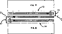
In Fig. 4 a, manufacturing comprises the method for the bonded substrate of at least one an active substrate A and a base substrate B, is included in to make first multilayer laminated 15 and make second multilayer laminated 17 on the installation surface of base substrate B on the bonding surface 12 of active substrate A.By means of on bonding surface 12, being deposited with the alternating layer that first material 11 and second material 13 are formed, make first multilayer laminated 15.Equally, by means of on installation surface 14, being deposited with the alternating layer that first material 11 and second material 13 are formed, make second multilayer laminated 17.
Table 1
| The material of |
| Selenium (Se) |
| Selenium-tellurium (SeTe) |
Table 2
| The material of |
| Indium (In) |
| Gallium (Ga) |
| Antimony (Sb) |
| Aluminium (Al) |
Can come deposit first and second multilayer laminated (15,17) with sputter or physical vapor deposition (PVD, for example electron beam evaporation) method.If first and second materials (11,13) are element compound (that is will form the polycrystalline compounds bonded layer), then PVD is preferred deposition technology.On the other hand, if first and second materials (11,13) are decrystallized compound (that is will form the amorphous compound bonded layer), then sputter is preferred deposition technology.An advantage that adopts sputter or PVD is enough lower temperature to realize deposit.
Though Fig. 4 a shows first material 11 and contacts with bonding surface 12, and second material 13 contacts with installation surface 14, the deposition sequence of the alternating layer of being made up of first material 11 and second material 13 can be inverted.That is, can deposit on bonding surface 12 and the installation surface 14 layer formed of the layer formed of first material 11 or second material 13.Therefore, aspect the deposition sequence of the alternating layer of forming by first material 11 and second material 13 and the number aspect of alternating layer, very big flexibility is arranged.For example, in Fig. 4 a, two layers being made up of first material 11 and second material 13 are deposited on respectively on bonding surface and the installation surface (12,14).On the other hand, in Fig. 4 b, first on the bonding surface 12 multilayer laminated 15 is made up of 3 layers, and second on the installation surface 14 multilayer laminated 17 is made up of 4 layers.
Fig. 4 b further illustrates this flexibility, and wherein first multilayer laminated 15 comprises alternating layer (11,13,11), and second multilayer laminated 17 comprises alternating layer (11,13,11,13).In Fig. 4 b, the two all has deposit first material layer 11 thereon bonding surface 12 and installation surface 14.On the contrary, in Fig. 4 a, bonding surface 12 has the layer that deposit first material 11 is thereon formed, and installation surface 14 has the layer that deposit second material 13 is thereon formed.
Can deposit first and second multilayer laminated (15,17) in comprising about 0.0-50.0 ℃ wide low temperature range.For example, can be in room temperature (about 25.0 ℃) deposit first and second multilayer laminated (15,17) down.An advantage of low deposition temperature is to high temp. sensitive or may be suitable for substrate bonding method of the present invention by the component of high-temperature damage.On the contrary, as mentioned above, these components may be not suitable for the high temperature of prior art method of wafer bonding.Though can be used to deposit first and second multilayer laminated (15,17) than above-mentioned higher temperature, not need to do like this.
The thickness of first material 11 and second material 13 can change in multilayer laminated first and second.That is first material 11 can have identical thickness with second material 13, also can have different thickness.The thickness of first material 11 and second material 13 is preferably in the scope interior (that is about 0.005-0.20 μ m) of about 50-2000 .
In Fig. 4 b, in deposit first and second multilayer laminated (15,17) afterwards, shown in dotted arrow C, first and second multilayer laminated (15,17) are contacted with each other.Therefore, in Fig. 5, the outermost layer of first material 11 in first multilayer laminated 15 contacts with the outermost layer of second multilayer laminated 17 second material 13, and (A determines an interface I (shown in dotted line) between B) in active substrate and base substrate.
Another advantage of the method for manufacturing bonded substrate of the present invention is, need not exert pressure to active substrate A and base substrate B basically, and first and second multilayer laminated (15,17) are contacted with each other.Thereby also under high pressure do not contact with each other, so with substrate distortion, crack, break or problem that stress is relevant is eliminated because substrate is not compelled to engage each other.Be generally used for microelectronics and dispose equipment with the semi-conducting material of location such as semiconductor wafer in making, can be used to make first and second multilayer laminated (15,17) to contact with each other and one or more active substrate A are aimed at base substrate B.Because the combination quality of one or more active substrate A and they first multilayer laminated 15 quality separately has some pressure and is applied on the base substrate B by active substrate A.But the desired high pressure of prior art wafer bonding technology that compares, this pressure is small.
In Fig. 6, by means of (A B) anneals, so that form compound bonded layer 19 by the selenylation reaction between the alternating layer of first and second materials (11,13) composition, active substrate A and base substrate B quilt be bonding each other to substrate in inert atmosphere.The result of selenylation reaction be compound bonded layer 19 with active substrate A and base substrate B bonding adhering to each other, thereby form bonded substrate 10.
If first material 11 is selenium (Se), and second material 13 is indium (In), and then compound bonded layer 19 is including, but not limited to such as InSe and In
5Se
6And so on the indium selenium compound (In of compound
xSe
y).
By means of (A B) heats, and can realize substrate (A, annealing B) to substrate under about 200-300 ℃ temperature.Inert atmosphere can be nitrogen (Ni) atmosphere for example.
Use element compound as first and second materials (11,13), cause polycrystalline compounds bonded layer 19.For example, if elemental selenium (Se) is used as first material 11, and element indium (In) is used as second material 13, and then annealing steps causes indium-selenium (In
xSe
y) polycrystalline compounds bonded layer (seeing the reference number 19 of Fig. 6).
On the contrary, use amorphous compound, cause amorphous compound bonded layer 19 as first and second materials (11,13).For example, if amorphous selenium (Se) is used as first material 11, and amorphous indium (In) is used as second material 13, and then annealing steps causes indium selenium (In
xSe
y) amorphous compound bonded layer (seeing the reference number 19 of Fig. 6).
In one embodiment of the invention, tellurium (Te) is added in the selenium (Se) of first material 11, to form selenium-tellurium (SeTe) layer.Tellurium (Te) be introduced in the selenium (Se) of first material 11 in first and second multilayer laminated (15,17) one or two.Therefore, by means of going up the alternating layer that deposit is made up of the selenium-tellurium (SeTe) and second material 13, first and second multilayer laminated (15,17) have been formed at bonding surface and installation surface (12,14).Second material 13 can be an indium (In) for example.Can deposit first and second multilayer laminated (15,17) in comprising about 0.0-50.0 ℃ temperature range.For example, can be in room temperature (about 25.0 ℃) deposit first and second multilayer laminated (15,17) down.
The thickness of selenium-tellurium (SeTe) layer and second material 13 can first and second multilayer laminated in variation.That is the selenium of first material 11-tellurium layer can have identical thickness with second material 13, also can have different thickness.The thickness of first material 11 and second material 13 is preferably in the scope interior (that is about 0.005-0.20 μ m) of about 50-2000 .
Then, in the above with reference to (A B) anneals to substrate in the described inert atmosphere of Fig. 6.If second material 13 comprises indium (In), then this annealing is owing to the selenylation reaction between the alternating layer of selenium-tellurium (SeTe) and indium (In) composition forms indium-selenium-tellurium (In
xSe
yTe
z, In
2Se
3-xTe
x, X<1) and compound bonded layer 19.The result of selenylation reaction is that indium-selenium-tellurium compound bonded layer 19 makes active substrate A and base substrate B bonding adhering to each other, thereby forms bonded substrate 10.Comprise the material that table 2 is cited, can replace the indium (In) of second material.
At the above-mentioned indium-selenium-tellurium (In that comprises
xSe
yTe
z, In
2Se
3-xTe
x, X<1) and among the embodiment of compound bonded layer 19, can be by means of (A B) heats and finishes substrate (A, annealing B) to substrate under about 150-300 ℃ temperature.Inert atmosphere can be nitrogen (Ni) atmosphere for example.
An advantage that tellurium (Te) is joined in the selenium (Se) of first material 11 is that the low side of annealing temperature can reduce about 50.0 ℃, thereby has reduced the heat arrangement of substrate annealing.That is, be reduced to 150 ℃ new low side (Te adds among the Se) from previous about 200 ℃ low side (not having Te to join the Se).The result, the adding of tellurium (Te) can realize substrate bonding under lower temperature, and this lower temperature may be favourable to some temperature sensitive application, in these are used, in order to prevent to damage the element of waiting to want the substrate of bonding or being waited to want the substrate supporting of bonding, must under about 150 ℃ temperature, carry out substrate bonding.Various elements, including, but not limited to as just transducer, accelerometer, actuator, pressure sensor, micromechanics, electrical micro-machine, electron emission device, optical element and the photoelectric cell of some examples and the phase transformation medium that is used for storing data, can both be waited to want the substrate supporting of bonding, be mounted thereon, or be embedded in wherein.
Use element compound as first and second materials (11,13), cause polycrystalline compounds bonded layer 19.For example, if elemental selenium-tellurium (SeTe) is used as first material 11, and element indium (In) is used as second material 13, and then annealing steps causes indium-selenium-tellurium (In
xSe
yTe
z, In
2Se
3-xTe
x, X<1) and compound bonded layer 19.
On the contrary, use amorphous compound, cause amorphous compound bonded layer 19 as first and second materials (11,13).For example, if amorphous selenium-tellurium (SeTe) is used as first material 11, and amorphous indium (In) is used as second material 13, and then annealing steps causes indium-selenium-tellurium (In
xSe
yTe
z, In
2Se
3-xTe
x, X<1) and compound bonded layer 19.
Indium-selenium-tellurium (In
xSe
yTe
z, In
2Se
3-xTe
x, X<1) and compound bonded layer 19 and (Se
xTe
y) to also have an advantage be can be with various backing materials bonding each other for compound bonded layer 19.Active substrate A can be made by identical materials or different materials with base substrate B.On the base substrate B shown in Fig. 9 a and 9b, be equipped with among the embodiment of a plurality of active substrates and/or by bonding each other and be bonded among the embodiment of the 3-D stacks that the active substrate of base substrate B forms, situation also is like this.
Active substrate A and base substrate B can be made by various materials, including, but not limited to silicon (Si), the silica (SiO that comprises silicon wafer
2), aluminium oxide (Al
2O
3) and the GaAs (GaAs) that comprises gallium arsenide wafer.Other material of active substrate A and base substrate B is including, but not limited to metal, the semi-conducting material that comprises semiconductor wafer and dielectric material.Active substrate A and base substrate B shape depend on and use and by the type of the element of active substrate A and base substrate B carrying.But the semiconductor wafer such as monocrystalline silicon (Si) wafer is owing to ready-made being very suitable for disposed becomes active substrate A and base substrate B with the microelectronics manufacturing equipment of processing semiconductor wafer and technology basis a kind of good selection is arranged.
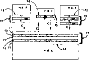
Fig. 7 a, 7b and 9a show another advantage of the present invention, and wherein shown in Fig. 7 a, the method for making bonded substrate is suitable for a plurality of (showing three) active substrate A, D and E are bonded to base substrate B.The size of active substrate A, D and E can change or be identical.And shown in Fig. 7 a, first multilayer laminated 15 of active substrate A, D and E can change first and second materials (11,13) layers in its deposition sequence on bonding surface 12 separately.The number of alternating layer also can change.For example, active substrate A haves three layers, and active substrate D has 2 layers, and active substrate E has 4 layers.Can deposit first and second multilayer laminated (15,17) in being same as above-mentioned temperature range.
Shown in dotted arrow C, second on the base substrate B multilayer laminated 17 contacted with first multilayer laminated 15 of active substrate A, D and E, obtain the structure shown in Fig. 7 b.As mentioned above, do not need basically active substrate A, D and E and base substrate B are exerted pressure.Therefore, in Fig. 7 b, the outermost layer of first material 11 of active substrate A and D contacts with the outermost layer of first material 11 of base substrate B, and the outermost layer of second material 13 of active substrate E contacts with the outermost layer of first material 11 of base substrate B, determines an interface I (seeing dotted line) between active substrate and base substrate.
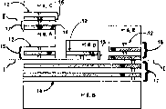
In Fig. 9 a, by means of in inert atmosphere, substrate (A, B, D and E) being annealed, selenylation reaction (as mentioned above) between the alternating layer of being made up of first material 11 and second material 13 forms compound bonded layer 19, thereby makes active substrate A, D, E and base substrate B bonding each other.The result of selenylation reaction is that compound bonded layer 19 makes active substrate A, D, E and base substrate B bonding adhering to each other, thereby forms bonded substrate 20.As mentioned above, compound bonded layer 19 can be polycrystalline compounds bonded layer 19 or amorphous compound bonded layer 19.
Fig. 8 a, 8b and 9b show another advantage of the present invention, wherein shown in Fig. 8 a, the method of making bonded substrate is suitable for a plurality of (showing three) active substrate A, D and E are bonded to base substrate B, and with a plurality of (showing two) active substrate A and C bonding each other.As active substrate A and C each other during bonding, they form 3-D stacks 22 (seeing Fig. 9 b).The size of active substrate A, C, D and E can change or be identical.And, as top with reference to as described in Fig. 7 a, 7b and the 9a, first and second materials (11,13) layer its separately the deposition sequence on the bonding surface 12 can change, the number of alternating layer also can change.
Shown in dotted arrow C, on the base substrate B second multilayer laminated 17 contacted with first multilayer laminated 15 of active substrate A, D and E, and first multilayer laminated 15 of active substrate C is contacted with second multilayer laminated 17 of active substrate A, obtain the structure shown in Fig. 8 b.As mentioned above, do not need basically active substrate A, C, D and E and base substrate B are exerted pressure.Therefore, in Fig. 8 b, the outermost layer of first material 11 of active substrate A and D contacts with the outermost layer of first material 11 of base substrate B, and the outermost layer of second material 13 of active substrate E contacts with the outermost layer of first material 11 of base substrate B, determines an interface I (seeing dotted line) between active substrate and base substrate.Equally, the outermost layer of second material 13 of active substrate C contacts with the outermost layer of first material 11 of active substrate A, active substrate (A determines an interface I between C) ' (seeing dotted line).
In Fig. 9 b, by means of in inert atmosphere, substrate (A, B, D and E) being annealed, selenylation reaction (as mentioned above) between the alternating layer of being made up of first material 11 and second material 13 forms compound bonded layer 19, thereby makes active substrate A, C, D, E and base substrate B bonding each other.The result of selenylation reaction is, compound bonded layer 19 makes active substrate, and (A, C) bonding adhering to each other, and make active substrate A, D, E and base substrate B bonding adhering to each other have the bonded substrate 30 of a plurality of active substrates and 3-D stacks 22 thereby form.Importantly, according to the present invention with selenylation reaction with active substrate bonding to the method for base substrate, also be suitable for a plurality of active substrates each other bonding to form 3-D stacks 22.Therefore, in Fig. 8 a, 8b and 9b, active substrate A is as the base substrate of active substrate C.Though in 3-D stacks 22, only show two active substrates (A, C), the structure shown in 3-D stacks 22 of the present invention is not limited to but can hold a plurality of active substrates.As mentioned above, in the embodiment shown in Fig. 9 a and the 9b, compound bonded layer 19 can be polycrystalline compounds bonded layer 19 or amorphous compound bonded layer 19.
As following with reference to Figure 10 a-10c, Figure 11 a-11c and Figure 12 a-12c will as described in, compound bonded layer 19 of the present invention (amorphous or polycrystalline) provides extra advantage, promptly can be dissolved, cause active substrate and the base substrate can be separated from one another by non-destructive ground.
Figure 10 a-10c shows the method that non-destructive ground separates the bonded substrate 10 that comprises at least one an active substrate A and a base substrate B.Active substrate and base substrate (A, B) combined thing bonded layer 19 bondings adhering to each other.As mentioned above, the material of compound bonded layer 19 can comprise indium-selenium-tellurium (In
xSe
yTe
z, In
2Se
3-xTe
x, X<1) and compound bonded layer 19 and/or (In
xSe
y) compound bonded layer 19.
Active and base substrate (A separated from one another, B) technology comprises by means of compound bonded layer 19 being exposed to optionally dissolved compound bonded layer 19 and does not impact or damage active and base substrate (A, selective wet etching material 27 B) and compound bonded layer 19 is carried out selective corrosion.For example, wet etching material 27 can be a kind of acid.The suitable selectivity corrosion material is including, but not limited to cited those of following table 3.
Table 3
| Be used for the selective |
| H 2SO 4 |
| HCl |
| HNO 3 |
| H 2PO 4 |
In Figure 10 b, bonded substrate 10 is placed in the container 25, and selective wet etching material 27 is introduced into container 25.As arrow S
dShown in, selective wet etching material 27 is dissolved compound bonded layer 19 optionally, and until shown in Figure 10 c, selective wet etching material 27 has dissolved all compound bonded layers 19 basically, make active and base substrate (A is B) no longer each other till the bonding.
Equally, in Figure 11 a-11c, bonded substrate 20 comprises that a plurality of combined thing bonded layer 19 adhesive bonds are incorporated into the active substrate (A, D and E) of base substrate B.In Figure 11 b, bonded substrate 20 is placed in the container 25, and selective wet etching material 27 is introduced into container 25.As arrow S
dShown in, selective wet etching material 27 is dissolved compound bonded layer 19 optionally, until shown in Figure 11 c, selective wet etching material 27 has dissolved all compound bonded layers 19 basically, makes active and base substrate (A, D, E and B) no longer each other till the bonding.
At last, in Figure 12 a-12c, bonded substrate 30 comprises that a plurality of combined thing bonded layer 19 adhesive bonds are incorporated into the active substrate (A, D and E) of base substrate B and the active substrate (A, C) of a plurality of combined thing bonded layer 19 bondings adhering to each other, thereby forms 3-D stacks 22.In Figure 12 b, bonded substrate 30 is placed in the container 25, and selective wet etching material 27 is introduced into container 25.As arrow S
dShown in, selective wet etching material 27 is dissolved compound bonded layer 19 optionally, until shown in Figure 12 c, selective wet etching material 27 has dissolved all compound bonded layers 19 basically, makes active and base substrate (A, C, D, E and B) no longer each other till the bonding.
In another embodiment of the present invention, shown in Figure 13 a-13c, replace deposit amorphous compound (11 as top combination forms amorphous compound bonded layer 19,13) alternating layer of Zu Chenging forms first and second multilayer laminated (15,17), each amorphous compound is deposited simultaneously and forms single amorphous layer.In Figure 13 a, active substrate A comprises first amorphous layer 7 that is produced on the bonding surface 12, and base substrate B comprises second amorphous layer 9 that is produced on the installation surface 14.
As mentioned above, can be at deposit first and second amorphous layers (7,9) in about 0.0-50.0 ℃ the temperature range.For example, can be at deposit first and second amorphous layers (7,9) under the room temperature (about 25.0 ℃).
Forming first and second amorphous layers (7,9) afterwards, making first and second amorphous layers (7,9) contact with each other (seeing the arrow C among Figure 13 a-13c).As mentioned above, when making first and second amorphous layers (7,9) when contacting with each other, do not need basically active substrate A and base substrate B are exerted pressure.
Then, by means of (A B) anneals to active substrate and base substrate in inert atmosphere, by first and second amorphous layers (7,9) selenylation reaction between forms compound bonded layer (seeing the reference number 19 among Fig. 6), thereby makes active substrate (A, B) bonding each other.Selenylation reaction makes active substrate and base substrate (A, B) bonding adhering to each other.Sputter is to be used for the optimization technique of deposit first and second amorphous layers (7,9).
First and second amorphous layers (7,9) can be by making including, but not limited to table 1 and the cited amorphous compound of table 2.Therefore, the amorphous compound of first and second amorphous layers (7,9) can comprise selenium (Se) and other material such as indium (In), gallium (Ga), antimony (Sb) and aluminium (Al).For example, if amorphous selenium (Se) and amorphous indium (In) are used to first and second amorphous layers (7,9), then annealing steps obtains indium-selenium (In
xSe
y) amorphous compound bonded layer (seeing the reference number 19 of Fig. 6).
(A B), can finish active substrate and base substrate (A, annealing B), thereby formation amorphous compound bonded layer 19 by means of active substrate of heating and base substrate under about 200-300 ℃ temperature.
In another embodiment of the present invention, first and second amorphous layers (7,9) can comprise selenium (Se) and tellurium (Te) (that is selenium-tellurium) and other material such as indium (In), gallium (Ga), antimony (Sb) and aluminium (Al).For example, if amorphous selenium-tellurium (SeTe) and amorphous indium (In) are used as first and second amorphous layers (7,9), then annealing steps causes indium-selenium-tellurium (In
xSe
yTe
z, In
2Se
3-xTe
x, X<1) and compound bonded layer (seeing the reference number 19 of Fig. 6).
When tellurium (Te) is added in the selenium (Se), can (A, (A, annealing B) form amorphous compound bonded layer 19 B) to finish substrate by means of heated substrate under about 150-300 ℃ temperature.As previously described, tellurium (Te) is added into the heat arrangement that makes annealing in the selenium (Se) and is reduced to lower about 150 ℃ from about 200 ℃.In above-mentioned two embodiment, the inert atmosphere of annealing process can be nitrogen (Ni) atmosphere for example.
The thickness of first and second amorphous layers (7,9) can change in first and second amorphous layers (7,9).That is first amorphous layer 7 can have identical thickness or different thickness with second amorphous layer 9.The thickness of first amorphous layer 7 and second amorphous layer 9 preferably is about 50-8000 (that is being about 0.005-0.80 μ m).
Active substrate and base substrate (A, material B) can be same as listed above, and active substrate and base substrate (A B) can be made by identical or different materials.
Figure 13 b shows and uses above-mentioned first and second amorphous layers (7,9) that a plurality of active substrate A, D and E are bonded to base substrate B.After active substrate and base substrate were annealed, first and second amorphous layers (7,9) formed amorphous compound bonded layer (seeing the reference number 19 among Fig. 9 a).
As mentioned above, in Figure 13 c, above-mentioned first and second amorphous layers (7,9) are bonded to base substrate B with a plurality of active substrate A, D and E, and active substrate C is bonded to active substrate A, thereby form 3-D stacks (seeing the reference number 22 among Fig. 9 b).After substrate was annealed, first and second amorphous layers (7,9) formed amorphous compound bonded layer (seeing the reference number 19 among Fig. 9 b).
For the described embodiment of Figure 13 a-13c, with reference to as described in Figure 10 a-12c,, can separate active substrate and base substrate in non-destructive ground by means of with selective corrosion material 27 dissolving amorphous compound bonded layers 19 as top.
Among described herein all embodiment, comprise those with active substrate more than or 3-D stacks, (A, B) in one or two can reduce active substrate and base substrate (A, thickness B) by means of the active substrate of attenuate and base substrate.The attenuate step can be in that (A B) carries out before the bonding each other, or (A B) carries out after being bonded each other in active substrate and base substrate with active substrate and base substrate.Normally used reduction process in the microelectric technique can be used to reduce active substrate and base substrate (A, thickness B).These technologies are including, but not limited to grinding, polishing and chemico-mechanical polishing (CMP).In addition, reduction process can be used to leveling (that is making it smooth basically) active substrate and base substrate (A, surface B).
Though disclose and described several embodiments of the present invention, the present invention is not limited to concrete form and arrangement disclosed herein and that describe.The present invention is only limited by the claims.
Claims (13)
1. method of making bonded substrate, this bonded substrate comprises at least one an active substrate (A) and a base substrate (B), the method comprises:
Form first multilayer laminated (15) by means of go up the alternating layer that deposit is made up of first material (11) and second material (13) at the bonding surface (12) of active substrate (A),
First material (11) comprises selenium, and
Second material (13) comprises the material that is selected from indium, gallium, antimony, aluminium;
Form second multilayer laminated (17) by means of go up the alternating layer that deposit is made up of first material (11) and second material (13) in the installation surface (14) of base substrate (B);
First and second multilayer laminated (15,17) are contacted with each other; And
By means of in inert atmosphere to substrate (A B) anneals, with form with substrate (A, B) the compound bonded layer (19) of bonding adhering to each other, thereby with active substrate and base substrate (A, B) bonding each other.
2. the described method of claim 1, annealing steps wherein are included in that (A B) heats to substrate under 200-300 ℃ the temperature.
3. the described method of claim 1 wherein by the alternating layer of first and second multilayer laminated (15,17) composition, is deposited under 0.0-50.0 ℃ temperature.
4. the described method of claim 1, first material (11) wherein also comprises tellurium.
5. the described method of claim 4, annealing steps wherein are included in that (A B) heats to substrate under 150-300 ℃ the temperature.
6. the described method of claim 4 wherein by the alternating layer of first and second multilayer laminated (15,17) composition, is deposited under 0.0-50.0 ℃ temperature.
7. the described method of claim 1, wherein active substrate (A) and base substrate (B) are the materials that is selected from semiconductor, metal, medium.
8. the described method of claim 1, wherein active substrate (A) and base substrate (B) are the materials that is selected from silicon, silica, aluminium oxide, GaAs.
9. the described method of claim 1, wherein active substrate (A) and base substrate (B) are made from a variety of materials.
10. the described method of claim 1, wherein active substrate (A) and base substrate (B) are made by identical materials.
11. the described method of claim 1 is wherein placed step and is comprised and first and second multilayer laminated (15,17) are contacted with each other and (A B) does not exert pressure to active substrate and base substrate basically.
12. the described method of claim 1, first material (11) wherein, second material (13) and compound bonded layer (19) are to be selected from the element material that becomes first material (11) and second material (13), to become the polycrystalline compounds bonded layer of compound bonded layer (19) and be selected from the amorphous compound that becomes first material (11) and second material (13), the amorphous compound bonded layer that becomes compound bonded layer (19).
13. the described method of claim 1, wherein the formation of first and second multilayer laminated (15,17) also comprises:
Go up formation first multilayer laminated (15) at the bonding surface (12) of at least one active substrate;
Installation surface (14) at another active substrate goes up formation second multilayer laminated (17);
First and second multilayer laminated (15,17) are contacted with each other; And
By means of in inert atmosphere, active substrate being annealed,, thereby form the 3-D stacks that active substrate is formed with the compound bonded layer (19) of formation with active substrate bonding adhering to each other.
Applications Claiming Priority (2)
| Application Number | Priority Date | Filing Date | Title |
|---|---|---|---|
| US09/823,550 US6537846B2 (en) | 2001-03-30 | 2001-03-30 | Substrate bonding using a selenidation reaction |
| US09/823550 | 2001-03-30 |
Publications (2)
| Publication Number | Publication Date |
|---|---|
| CN1379436A CN1379436A (en) | 2002-11-13 |
| CN1286145C true CN1286145C (en) | 2006-11-22 |
Family
ID=25239072
Family Applications (1)
| Application Number | Title | Priority Date | Filing Date |
|---|---|---|---|
| CNB021032106A Expired - Fee Related CN1286145C (en) | 2001-03-30 | 2002-01-30 | Substrate linkage using selenylation reaction |
Country Status (5)
| Country | Link |
|---|---|
| US (1) | US6537846B2 (en) |
| EP (1) | EP1246238B1 (en) |
| JP (1) | JP4198375B2 (en) |
| CN (1) | CN1286145C (en) |
| DE (1) | DE60220736T2 (en) |
Families Citing this family (20)
| Publication number | Priority date | Publication date | Assignee | Title |
|---|---|---|---|---|
| US6362075B1 (en) * | 1999-06-30 | 2002-03-26 | Harris Corporation | Method for making a diffused back-side layer on a bonded-wafer with a thick bond oxide |
| JP2002305293A (en) * | 2001-04-06 | 2002-10-18 | Canon Inc | Method of manufacturing semiconductor member, and method of manufacturing semiconductor device |
| US6960490B2 (en) * | 2002-03-14 | 2005-11-01 | Epitactix Pty Ltd. | Method and resulting structure for manufacturing semiconductor substrates |
| US7192841B2 (en) * | 2002-04-30 | 2007-03-20 | Agency For Science, Technology And Research | Method of wafer/substrate bonding |
| EP1477792B1 (en) * | 2003-05-13 | 2006-10-25 | Becton, Dickinson and Company | Method and apparatus for purifying and desalting biological samples |
| US7176106B2 (en) * | 2003-06-13 | 2007-02-13 | Avago Technologies Fiber Ip (Singapore) Pte. Ltd. | Wafer bonding using reactive foils for massively parallel micro-electromechanical systems packaging |
| US7407863B2 (en) | 2003-10-07 | 2008-08-05 | Board Of Trustees Of The University Of Illinois | Adhesive bonding with low temperature grown amorphous or polycrystalline compound semiconductors |
| US7026189B2 (en) * | 2004-02-11 | 2006-04-11 | Hewlett-Packard Development Company, L.P. | Wafer packaging and singulation method |
| US7422962B2 (en) * | 2004-10-27 | 2008-09-09 | Hewlett-Packard Development Company, L.P. | Method of singulating electronic devices |
| FR2888402B1 (en) * | 2005-07-06 | 2007-12-21 | Commissariat Energie Atomique | METHOD FOR ASSEMBLING SUBSTRATES BY DEPOSITING A THIN OXIDE OR NITRIDE BONDING LAYER AND STRUCTURE THUS ASSEMBLED |
| KR100829562B1 (en) * | 2006-08-25 | 2008-05-14 | 삼성전자주식회사 | Semiconductor laser diode having wafer-bonded structure and method of fabricating the same |
| US20100109115A1 (en) * | 2008-11-03 | 2010-05-06 | Ure Michael J | Virtual IC wafers and bonding of constitutent IC films |
| US8748288B2 (en) * | 2010-02-05 | 2014-06-10 | International Business Machines Corporation | Bonded structure with enhanced adhesion strength |
| EP2597670B1 (en) * | 2010-03-31 | 2016-03-30 | EV Group E. Thallner GmbH | Method for permanently connecting two metal surfaces |
| US9117948B1 (en) | 2012-02-02 | 2015-08-25 | The United States Of America As Represented By The Adminstrator Of National Aeronautics And Space Administration | Selenium interlayer for high-efficiency multijunction solar cell |
| US10615191B2 (en) | 2016-05-20 | 2020-04-07 | Ares Materials Inc. | Polymer substrate for flexible electronics microfabrication and methods of use |
| US10736212B2 (en) | 2016-05-20 | 2020-08-04 | Ares Materials Inc. | Substrates for stretchable electronics and method of manufacture |
| WO2018029594A1 (en) * | 2016-08-09 | 2018-02-15 | King Abdullah University Of Science And Technology | A semiconductor device including monolithically integrated pmos and nmos transistors |
| CN107742606B (en) * | 2017-10-30 | 2024-04-02 | 桂林电子科技大学 | Structure for bonding wafers and preparation method thereof |
| CN110534644B (en) * | 2019-08-30 | 2021-01-15 | 华中科技大学 | Preparation method of bidirectional-growth superlattice phase change unit and phase change memory |
Family Cites Families (13)
| Publication number | Priority date | Publication date | Assignee | Title |
|---|---|---|---|---|
| JPS61182217A (en) * | 1985-02-08 | 1986-08-14 | Toshiba Corp | Bonding method of wafer |
| JPH0472608A (en) * | 1990-05-18 | 1992-03-06 | Toshiba Corp | Manufacturing process and device compound semiconductor wafer |
| JP2990036B2 (en) | 1995-02-13 | 1999-12-13 | ティーディーケイ株式会社 | Optical recording medium and manufacturing method thereof |
| JPH08316145A (en) * | 1995-05-12 | 1996-11-29 | Fuji Electric Co Ltd | Method for forming semiconductor thin film |
| US5730852A (en) | 1995-09-25 | 1998-03-24 | Davis, Joseph & Negley | Preparation of cuxinygazsen (X=0-2, Y=0-2, Z=0-2, N=0-3) precursor films by electrodeposition for fabricating high efficiency solar cells |
| JP2737748B2 (en) * | 1996-06-21 | 1998-04-08 | 日本電気株式会社 | Compound semiconductor bonding method |
| FR2751467B1 (en) * | 1996-07-17 | 1998-10-02 | Commissariat Energie Atomique | METHOD FOR ASSEMBLING TWO STRUCTURES AND DEVICE OBTAINED BY THE METHOD. MICROLASER APPLICATIONS |
| JP3249408B2 (en) | 1996-10-25 | 2002-01-21 | 昭和シェル石油株式会社 | Method and apparatus for manufacturing thin film light absorbing layer of thin film solar cell |
| US6036772A (en) | 1996-12-30 | 2000-03-14 | Sony Corporation | Method for making semiconductor device |
| US6258620B1 (en) * | 1997-10-15 | 2001-07-10 | University Of South Florida | Method of manufacturing CIGS photovoltaic devices |
| US6323417B1 (en) * | 1998-09-29 | 2001-11-27 | Lockheed Martin Corporation | Method of making I-III-VI semiconductor materials for use in photovoltaic cells |
| JP2000349266A (en) * | 1999-03-26 | 2000-12-15 | Canon Inc | Manufacture of semiconductor member, utilization method for semiconductor basic substance, manufacture system for semiconductor member, production control method therefor and utilizing method for forming device for film depositing |
| JP4465745B2 (en) * | 1999-07-23 | 2010-05-19 | ソニー株式会社 | Semiconductor laminated substrate, semiconductor crystal substrate, semiconductor element, and manufacturing method thereof |
-
2001
- 2001-03-30 US US09/823,550 patent/US6537846B2/en not_active Expired - Fee Related
-
2002
- 2002-01-30 CN CNB021032106A patent/CN1286145C/en not_active Expired - Fee Related
- 2002-03-29 JP JP2002093974A patent/JP4198375B2/en not_active Expired - Fee Related
- 2002-04-02 DE DE60220736T patent/DE60220736T2/en not_active Expired - Lifetime
- 2002-04-02 EP EP02252376A patent/EP1246238B1/en not_active Expired - Fee Related
Also Published As
| Publication number | Publication date |
|---|---|
| EP1246238A3 (en) | 2003-11-26 |
| US6537846B2 (en) | 2003-03-25 |
| JP4198375B2 (en) | 2008-12-17 |
| EP1246238A2 (en) | 2002-10-02 |
| DE60220736T2 (en) | 2008-03-13 |
| JP2003017375A (en) | 2003-01-17 |
| CN1379436A (en) | 2002-11-13 |
| DE60220736D1 (en) | 2007-08-02 |
| EP1246238B1 (en) | 2007-06-20 |
| US20030017679A1 (en) | 2003-01-23 |
Similar Documents
| Publication | Publication Date | Title |
|---|---|---|
| CN1286145C (en) | Substrate linkage using selenylation reaction | |
| CN112020763B (en) | DBI to SI bonding for simplified handle wafer | |
| CN107034028B (en) | Composition for removing silicone resin, method for thinning substrate and manufacturing semiconductor package using the same, and system using the same | |
| US8377798B2 (en) | Method and structure for wafer to wafer bonding in semiconductor packaging | |
| KR100738145B1 (en) | Method for making substrate and resulting substrates | |
| CN101047170A (en) | Semiconductor device and manufacturing method thereof | |
| TWI604520B (en) | Multiple bonding layers for thin-wafer handling and temporary bonding methods | |
| US10121762B2 (en) | Wafer bonding structure and wafer bonding method | |
| EP1720204A1 (en) | Transient liquid phase eutectic bonding | |
| US8563400B2 (en) | Laser bonding for stacking semiconductor substrates | |
| JP2005516393A5 (en) | ||
| TW201001503A (en) | Wafer structures and wafer bonding methods | |
| CN1473361A (en) | Method for making stacked structure comprising thin film adhering to target substrate | |
| CN101043023A (en) | Method for forming a 3d integrated circuit | |
| TWI777986B (en) | Method and system for vertical integration of elemental and compound semiconductors | |
| TW201205688A (en) | Temporary semiconductor structure bonding methods and related bonded semiconductor structures | |
| US20130320071A1 (en) | Apparatus and Method of Substrate to Substrate Bonding for Three Dimensional (3D) IC Interconnects | |
| US10854494B2 (en) | Method for producing an interface intended to assemble temporarily a microelectronic support and a manipulation handle, and temporary assembly interface | |
| CN1233073A (en) | Semiconductor device and manufacturing method of same | |
| CN101069293A (en) | Micro-electromechanical device | |
| CN1716620A (en) | Semiconductor chip and method for manufacturing the same and semiconductor device | |
| CN1199254C (en) | Component and method for the production thereof | |
| US11165005B2 (en) | Method for producing a microelectronic chip to be hybridised to a second chip | |
| JP2004320050A (en) | Soi substrate and method for manufacturing same | |
| US20230207515A1 (en) | Method of assembly by direct bonding of electronic components |
Legal Events
| Date | Code | Title | Description |
|---|---|---|---|
| C06 | Publication | ||
| PB01 | Publication | ||
| C10 | Entry into substantive examination | ||
| SE01 | Entry into force of request for substantive examination | ||
| C14 | Grant of patent or utility model | ||
| GR01 | Patent grant | ||
| C17 | Cessation of patent right | ||
| CF01 | Termination of patent right due to non-payment of annual fee |
Granted publication date: 20061122 Termination date: 20110130 |