CN1265451C - Semiconductor device and manufactoring method thereof - Google Patents
Semiconductor device and manufactoring method thereof Download PDFInfo
- Publication number
- CN1265451C CN1265451C CNB011045531A CN01104553A CN1265451C CN 1265451 C CN1265451 C CN 1265451C CN B011045531 A CNB011045531 A CN B011045531A CN 01104553 A CN01104553 A CN 01104553A CN 1265451 C CN1265451 C CN 1265451C
- Authority
- CN
- China
- Prior art keywords
- mentioned
- electrode
- insulating properties
- semiconductor element
- felting cell
- Prior art date
- Legal status (The legal status is an assumption and is not a legal conclusion. Google has not performed a legal analysis and makes no representation as to the accuracy of the status listed.)
- Expired - Fee Related
Links
- 239000004065 semiconductor Substances 0.000 title claims abstract description 114
- 238000000034 method Methods 0.000 title claims description 24
- 239000011888 foil Substances 0.000 claims abstract description 49
- 229920005989 resin Polymers 0.000 claims abstract description 49
- 239000011347 resin Substances 0.000 claims abstract description 49
- 238000009950 felting Methods 0.000 claims description 61
- 238000003466 welding Methods 0.000 claims description 18
- 238000004519 manufacturing process Methods 0.000 claims description 17
- 229910052751 metal Inorganic materials 0.000 claims description 17
- 239000002184 metal Substances 0.000 claims description 17
- 239000007767 bonding agent Substances 0.000 claims description 5
- 239000000853 adhesive Substances 0.000 claims description 3
- 230000001070 adhesive effect Effects 0.000 claims description 3
- 239000000758 substrate Substances 0.000 abstract description 20
- 239000000919 ceramic Substances 0.000 abstract description 3
- 230000005855 radiation Effects 0.000 abstract description 3
- 239000000463 material Substances 0.000 description 14
- 238000005530 etching Methods 0.000 description 11
- 238000005520 cutting process Methods 0.000 description 10
- 238000009826 distribution Methods 0.000 description 10
- 239000011248 coating agent Substances 0.000 description 9
- 238000000576 coating method Methods 0.000 description 9
- 239000010949 copper Substances 0.000 description 6
- 229910000679 solder Inorganic materials 0.000 description 5
- 229910017767 Cu—Al Inorganic materials 0.000 description 4
- 239000004020 conductor Substances 0.000 description 4
- 229920002120 photoresistant polymer Polymers 0.000 description 4
- PNEYBMLMFCGWSK-UHFFFAOYSA-N Alumina Chemical compound [O-2].[O-2].[O-2].[Al+3].[Al+3] PNEYBMLMFCGWSK-UHFFFAOYSA-N 0.000 description 3
- RYGMFSIKBFXOCR-UHFFFAOYSA-N Copper Chemical compound [Cu] RYGMFSIKBFXOCR-UHFFFAOYSA-N 0.000 description 3
- 230000007797 corrosion Effects 0.000 description 3
- 238000005260 corrosion Methods 0.000 description 3
- 230000000694 effects Effects 0.000 description 3
- 238000005516 engineering process Methods 0.000 description 3
- 238000000926 separation method Methods 0.000 description 3
- 229920005992 thermoplastic resin Polymers 0.000 description 3
- 229920001187 thermosetting polymer Polymers 0.000 description 3
- 229910001030 Iron–nickel alloy Inorganic materials 0.000 description 2
- ATJFFYVFTNAWJD-UHFFFAOYSA-N Tin Chemical compound [Sn] ATJFFYVFTNAWJD-UHFFFAOYSA-N 0.000 description 2
- 229910045601 alloy Inorganic materials 0.000 description 2
- 239000000956 alloy Substances 0.000 description 2
- 238000013459 approach Methods 0.000 description 2
- 230000015572 biosynthetic process Effects 0.000 description 2
- 229910052802 copper Inorganic materials 0.000 description 2
- 239000003822 epoxy resin Substances 0.000 description 2
- 239000000945 filler Substances 0.000 description 2
- 229910052737 gold Inorganic materials 0.000 description 2
- 238000001746 injection moulding Methods 0.000 description 2
- 229920000647 polyepoxide Polymers 0.000 description 2
- 229920006389 polyphenyl polymer Polymers 0.000 description 2
- 238000005096 rolling process Methods 0.000 description 2
- 229910052709 silver Inorganic materials 0.000 description 2
- 238000005987 sulfurization reaction Methods 0.000 description 2
- 238000001721 transfer moulding Methods 0.000 description 2
- 229910018182 Al—Cu Inorganic materials 0.000 description 1
- 229920000106 Liquid crystal polymer Polymers 0.000 description 1
- 239000004977 Liquid-crystal polymers (LCPs) Substances 0.000 description 1
- -1 be soft board Substances 0.000 description 1
- 239000011889 copper foil Substances 0.000 description 1
- 239000012776 electronic material Substances 0.000 description 1
- 238000005538 encapsulation Methods 0.000 description 1
- 239000012850 fabricated material Substances 0.000 description 1
- 239000012530 fluid Substances 0.000 description 1
- 238000000227 grinding Methods 0.000 description 1
- 238000001802 infusion Methods 0.000 description 1
- 239000011810 insulating material Substances 0.000 description 1
- 239000003550 marker Substances 0.000 description 1
- 229910052759 nickel Inorganic materials 0.000 description 1
- 229910052763 palladium Inorganic materials 0.000 description 1
- 238000001259 photo etching Methods 0.000 description 1
- 238000007747 plating Methods 0.000 description 1
- 229920001721 polyimide Polymers 0.000 description 1
- 239000009719 polyimide resin Substances 0.000 description 1
- 238000004382 potting Methods 0.000 description 1
- 238000007639 printing Methods 0.000 description 1
- 238000004080 punching Methods 0.000 description 1
- 238000010008 shearing Methods 0.000 description 1
- 239000002893 slag Substances 0.000 description 1
- 239000000126 substance Substances 0.000 description 1
- 230000008646 thermal stress Effects 0.000 description 1
- 238000009736 wetting Methods 0.000 description 1
Images


Classifications
-
- H—ELECTRICITY
- H01—ELECTRIC ELEMENTS
- H01L—SEMICONDUCTOR DEVICES NOT COVERED BY CLASS H10
- H01L23/00—Details of semiconductor or other solid state devices
- H01L23/34—Arrangements for cooling, heating, ventilating or temperature compensation ; Temperature sensing arrangements
- H01L23/36—Selection of materials, or shaping, to facilitate cooling or heating, e.g. heatsinks
-
- H—ELECTRICITY
- H01—ELECTRIC ELEMENTS
- H01L—SEMICONDUCTOR DEVICES NOT COVERED BY CLASS H10
- H01L24/00—Arrangements for connecting or disconnecting semiconductor or solid-state bodies; Methods or apparatus related thereto
- H01L24/80—Methods for connecting semiconductor or other solid state bodies using means for bonding being attached to, or being formed on, the surface to be connected
- H01L24/83—Methods for connecting semiconductor or other solid state bodies using means for bonding being attached to, or being formed on, the surface to be connected using a layer connector
-
- H—ELECTRICITY
- H01—ELECTRIC ELEMENTS
- H01L—SEMICONDUCTOR DEVICES NOT COVERED BY CLASS H10
- H01L21/00—Processes or apparatus adapted for the manufacture or treatment of semiconductor or solid state devices or of parts thereof
- H01L21/02—Manufacture or treatment of semiconductor devices or of parts thereof
- H01L21/04—Manufacture or treatment of semiconductor devices or of parts thereof the devices having potential barriers, e.g. a PN junction, depletion layer or carrier concentration layer
- H01L21/48—Manufacture or treatment of parts, e.g. containers, prior to assembly of the devices, using processes not provided for in a single one of the subgroups H01L21/06 - H01L21/326
- H01L21/4814—Conductive parts
- H01L21/4821—Flat leads, e.g. lead frames with or without insulating supports
- H01L21/4828—Etching
- H01L21/4832—Etching a temporary substrate after encapsulation process to form leads
-
- H—ELECTRICITY
- H01—ELECTRIC ELEMENTS
- H01L—SEMICONDUCTOR DEVICES NOT COVERED BY CLASS H10
- H01L23/00—Details of semiconductor or other solid state devices
- H01L23/28—Encapsulations, e.g. encapsulating layers, coatings, e.g. for protection
- H01L23/31—Encapsulations, e.g. encapsulating layers, coatings, e.g. for protection characterised by the arrangement or shape
- H01L23/3107—Encapsulations, e.g. encapsulating layers, coatings, e.g. for protection characterised by the arrangement or shape the device being completely enclosed
-
- H—ELECTRICITY
- H01—ELECTRIC ELEMENTS
- H01L—SEMICONDUCTOR DEVICES NOT COVERED BY CLASS H10
- H01L23/00—Details of semiconductor or other solid state devices
- H01L23/48—Arrangements for conducting electric current to or from the solid state body in operation, e.g. leads, terminal arrangements ; Selection of materials therefor
- H01L23/488—Arrangements for conducting electric current to or from the solid state body in operation, e.g. leads, terminal arrangements ; Selection of materials therefor consisting of soldered or bonded constructions
- H01L23/495—Lead-frames or other flat leads
- H01L23/49503—Lead-frames or other flat leads characterised by the die pad
- H01L23/49513—Lead-frames or other flat leads characterised by the die pad having bonding material between chip and die pad
-
- H—ELECTRICITY
- H01—ELECTRIC ELEMENTS
- H01L—SEMICONDUCTOR DEVICES NOT COVERED BY CLASS H10
- H01L24/00—Arrangements for connecting or disconnecting semiconductor or solid-state bodies; Methods or apparatus related thereto
- H01L24/01—Means for bonding being attached to, or being formed on, the surface to be connected, e.g. chip-to-package, die-attach, "first-level" interconnects; Manufacturing methods related thereto
- H01L24/26—Layer connectors, e.g. plate connectors, solder or adhesive layers; Manufacturing methods related thereto
- H01L24/28—Structure, shape, material or disposition of the layer connectors prior to the connecting process
- H01L24/29—Structure, shape, material or disposition of the layer connectors prior to the connecting process of an individual layer connector
-
- H—ELECTRICITY
- H01—ELECTRIC ELEMENTS
- H01L—SEMICONDUCTOR DEVICES NOT COVERED BY CLASS H10
- H01L24/00—Arrangements for connecting or disconnecting semiconductor or solid-state bodies; Methods or apparatus related thereto
- H01L24/01—Means for bonding being attached to, or being formed on, the surface to be connected, e.g. chip-to-package, die-attach, "first-level" interconnects; Manufacturing methods related thereto
- H01L24/26—Layer connectors, e.g. plate connectors, solder or adhesive layers; Manufacturing methods related thereto
- H01L24/31—Structure, shape, material or disposition of the layer connectors after the connecting process
- H01L24/32—Structure, shape, material or disposition of the layer connectors after the connecting process of an individual layer connector
-
- H—ELECTRICITY
- H01—ELECTRIC ELEMENTS
- H01L—SEMICONDUCTOR DEVICES NOT COVERED BY CLASS H10
- H01L24/00—Arrangements for connecting or disconnecting semiconductor or solid-state bodies; Methods or apparatus related thereto
- H01L24/93—Batch processes
- H01L24/95—Batch processes at chip-level, i.e. with connecting carried out on a plurality of singulated devices, i.e. on diced chips
- H01L24/97—Batch processes at chip-level, i.e. with connecting carried out on a plurality of singulated devices, i.e. on diced chips the devices being connected to a common substrate, e.g. interposer, said common substrate being separable into individual assemblies after connecting
-
- H—ELECTRICITY
- H01—ELECTRIC ELEMENTS
- H01L—SEMICONDUCTOR DEVICES NOT COVERED BY CLASS H10
- H01L2221/00—Processes or apparatus adapted for the manufacture or treatment of semiconductor or solid state devices or of parts thereof covered by H01L21/00
- H01L2221/67—Apparatus for handling semiconductor or electric solid state devices during manufacture or treatment thereof; Apparatus for handling wafers during manufacture or treatment of semiconductor or electric solid state devices or components; Apparatus not specifically provided for elsewhere
- H01L2221/683—Apparatus for handling semiconductor or electric solid state devices during manufacture or treatment thereof; Apparatus for handling wafers during manufacture or treatment of semiconductor or electric solid state devices or components; Apparatus not specifically provided for elsewhere for supporting or gripping
- H01L2221/68304—Apparatus for handling semiconductor or electric solid state devices during manufacture or treatment thereof; Apparatus for handling wafers during manufacture or treatment of semiconductor or electric solid state devices or components; Apparatus not specifically provided for elsewhere for supporting or gripping using temporarily an auxiliary support
- H01L2221/68377—Apparatus for handling semiconductor or electric solid state devices during manufacture or treatment thereof; Apparatus for handling wafers during manufacture or treatment of semiconductor or electric solid state devices or components; Apparatus not specifically provided for elsewhere for supporting or gripping using temporarily an auxiliary support with parts of the auxiliary support remaining in the finished device
-
- H—ELECTRICITY
- H01—ELECTRIC ELEMENTS
- H01L—SEMICONDUCTOR DEVICES NOT COVERED BY CLASS H10
- H01L2224/00—Indexing scheme for arrangements for connecting or disconnecting semiconductor or solid-state bodies and methods related thereto as covered by H01L24/00
- H01L2224/01—Means for bonding being attached to, or being formed on, the surface to be connected, e.g. chip-to-package, die-attach, "first-level" interconnects; Manufacturing methods related thereto
- H01L2224/02—Bonding areas; Manufacturing methods related thereto
- H01L2224/04—Structure, shape, material or disposition of the bonding areas prior to the connecting process
- H01L2224/05—Structure, shape, material or disposition of the bonding areas prior to the connecting process of an individual bonding area
- H01L2224/0554—External layer
- H01L2224/0555—Shape
- H01L2224/05552—Shape in top view
- H01L2224/05554—Shape in top view being square
-
- H—ELECTRICITY
- H01—ELECTRIC ELEMENTS
- H01L—SEMICONDUCTOR DEVICES NOT COVERED BY CLASS H10
- H01L2224/00—Indexing scheme for arrangements for connecting or disconnecting semiconductor or solid-state bodies and methods related thereto as covered by H01L24/00
- H01L2224/01—Means for bonding being attached to, or being formed on, the surface to be connected, e.g. chip-to-package, die-attach, "first-level" interconnects; Manufacturing methods related thereto
- H01L2224/26—Layer connectors, e.g. plate connectors, solder or adhesive layers; Manufacturing methods related thereto
- H01L2224/28—Structure, shape, material or disposition of the layer connectors prior to the connecting process
- H01L2224/29—Structure, shape, material or disposition of the layer connectors prior to the connecting process of an individual layer connector
- H01L2224/29001—Core members of the layer connector
- H01L2224/29099—Material
- H01L2224/2919—Material with a principal constituent of the material being a polymer, e.g. polyester, phenolic based polymer, epoxy
-
- H—ELECTRICITY
- H01—ELECTRIC ELEMENTS
- H01L—SEMICONDUCTOR DEVICES NOT COVERED BY CLASS H10
- H01L2224/00—Indexing scheme for arrangements for connecting or disconnecting semiconductor or solid-state bodies and methods related thereto as covered by H01L24/00
- H01L2224/01—Means for bonding being attached to, or being formed on, the surface to be connected, e.g. chip-to-package, die-attach, "first-level" interconnects; Manufacturing methods related thereto
- H01L2224/26—Layer connectors, e.g. plate connectors, solder or adhesive layers; Manufacturing methods related thereto
- H01L2224/31—Structure, shape, material or disposition of the layer connectors after the connecting process
- H01L2224/32—Structure, shape, material or disposition of the layer connectors after the connecting process of an individual layer connector
- H01L2224/3205—Shape
- H01L2224/32057—Shape in side view
-
- H—ELECTRICITY
- H01—ELECTRIC ELEMENTS
- H01L—SEMICONDUCTOR DEVICES NOT COVERED BY CLASS H10
- H01L2224/00—Indexing scheme for arrangements for connecting or disconnecting semiconductor or solid-state bodies and methods related thereto as covered by H01L24/00
- H01L2224/01—Means for bonding being attached to, or being formed on, the surface to be connected, e.g. chip-to-package, die-attach, "first-level" interconnects; Manufacturing methods related thereto
- H01L2224/26—Layer connectors, e.g. plate connectors, solder or adhesive layers; Manufacturing methods related thereto
- H01L2224/31—Structure, shape, material or disposition of the layer connectors after the connecting process
- H01L2224/32—Structure, shape, material or disposition of the layer connectors after the connecting process of an individual layer connector
- H01L2224/321—Disposition
- H01L2224/32151—Disposition the layer connector connecting between a semiconductor or solid-state body and an item not being a semiconductor or solid-state body, e.g. chip-to-substrate, chip-to-passive
- H01L2224/32221—Disposition the layer connector connecting between a semiconductor or solid-state body and an item not being a semiconductor or solid-state body, e.g. chip-to-substrate, chip-to-passive the body and the item being stacked
- H01L2224/32225—Disposition the layer connector connecting between a semiconductor or solid-state body and an item not being a semiconductor or solid-state body, e.g. chip-to-substrate, chip-to-passive the body and the item being stacked the item being non-metallic, e.g. insulating substrate with or without metallisation
-
- H—ELECTRICITY
- H01—ELECTRIC ELEMENTS
- H01L—SEMICONDUCTOR DEVICES NOT COVERED BY CLASS H10
- H01L2224/00—Indexing scheme for arrangements for connecting or disconnecting semiconductor or solid-state bodies and methods related thereto as covered by H01L24/00
- H01L2224/01—Means for bonding being attached to, or being formed on, the surface to be connected, e.g. chip-to-package, die-attach, "first-level" interconnects; Manufacturing methods related thereto
- H01L2224/26—Layer connectors, e.g. plate connectors, solder or adhesive layers; Manufacturing methods related thereto
- H01L2224/31—Structure, shape, material or disposition of the layer connectors after the connecting process
- H01L2224/32—Structure, shape, material or disposition of the layer connectors after the connecting process of an individual layer connector
- H01L2224/321—Disposition
- H01L2224/32151—Disposition the layer connector connecting between a semiconductor or solid-state body and an item not being a semiconductor or solid-state body, e.g. chip-to-substrate, chip-to-passive
- H01L2224/32221—Disposition the layer connector connecting between a semiconductor or solid-state body and an item not being a semiconductor or solid-state body, e.g. chip-to-substrate, chip-to-passive the body and the item being stacked
- H01L2224/32245—Disposition the layer connector connecting between a semiconductor or solid-state body and an item not being a semiconductor or solid-state body, e.g. chip-to-substrate, chip-to-passive the body and the item being stacked the item being metallic
-
- H—ELECTRICITY
- H01—ELECTRIC ELEMENTS
- H01L—SEMICONDUCTOR DEVICES NOT COVERED BY CLASS H10
- H01L2224/00—Indexing scheme for arrangements for connecting or disconnecting semiconductor or solid-state bodies and methods related thereto as covered by H01L24/00
- H01L2224/01—Means for bonding being attached to, or being formed on, the surface to be connected, e.g. chip-to-package, die-attach, "first-level" interconnects; Manufacturing methods related thereto
- H01L2224/42—Wire connectors; Manufacturing methods related thereto
- H01L2224/44—Structure, shape, material or disposition of the wire connectors prior to the connecting process
- H01L2224/45—Structure, shape, material or disposition of the wire connectors prior to the connecting process of an individual wire connector
- H01L2224/45001—Core members of the connector
- H01L2224/45099—Material
- H01L2224/451—Material with a principal constituent of the material being a metal or a metalloid, e.g. boron (B), silicon (Si), germanium (Ge), arsenic (As), antimony (Sb), tellurium (Te) and polonium (Po), and alloys thereof
-
- H—ELECTRICITY
- H01—ELECTRIC ELEMENTS
- H01L—SEMICONDUCTOR DEVICES NOT COVERED BY CLASS H10
- H01L2224/00—Indexing scheme for arrangements for connecting or disconnecting semiconductor or solid-state bodies and methods related thereto as covered by H01L24/00
- H01L2224/01—Means for bonding being attached to, or being formed on, the surface to be connected, e.g. chip-to-package, die-attach, "first-level" interconnects; Manufacturing methods related thereto
- H01L2224/42—Wire connectors; Manufacturing methods related thereto
- H01L2224/47—Structure, shape, material or disposition of the wire connectors after the connecting process
- H01L2224/48—Structure, shape, material or disposition of the wire connectors after the connecting process of an individual wire connector
- H01L2224/4805—Shape
- H01L2224/4809—Loop shape
- H01L2224/48091—Arched
-
- H—ELECTRICITY
- H01—ELECTRIC ELEMENTS
- H01L—SEMICONDUCTOR DEVICES NOT COVERED BY CLASS H10
- H01L2224/00—Indexing scheme for arrangements for connecting or disconnecting semiconductor or solid-state bodies and methods related thereto as covered by H01L24/00
- H01L2224/01—Means for bonding being attached to, or being formed on, the surface to be connected, e.g. chip-to-package, die-attach, "first-level" interconnects; Manufacturing methods related thereto
- H01L2224/42—Wire connectors; Manufacturing methods related thereto
- H01L2224/47—Structure, shape, material or disposition of the wire connectors after the connecting process
- H01L2224/48—Structure, shape, material or disposition of the wire connectors after the connecting process of an individual wire connector
- H01L2224/481—Disposition
- H01L2224/48151—Connecting between a semiconductor or solid-state body and an item not being a semiconductor or solid-state body, e.g. chip-to-substrate, chip-to-passive
- H01L2224/48221—Connecting between a semiconductor or solid-state body and an item not being a semiconductor or solid-state body, e.g. chip-to-substrate, chip-to-passive the body and the item being stacked
- H01L2224/48225—Connecting between a semiconductor or solid-state body and an item not being a semiconductor or solid-state body, e.g. chip-to-substrate, chip-to-passive the body and the item being stacked the item being non-metallic, e.g. insulating substrate with or without metallisation
- H01L2224/48227—Connecting between a semiconductor or solid-state body and an item not being a semiconductor or solid-state body, e.g. chip-to-substrate, chip-to-passive the body and the item being stacked the item being non-metallic, e.g. insulating substrate with or without metallisation connecting the wire to a bond pad of the item
-
- H—ELECTRICITY
- H01—ELECTRIC ELEMENTS
- H01L—SEMICONDUCTOR DEVICES NOT COVERED BY CLASS H10
- H01L2224/00—Indexing scheme for arrangements for connecting or disconnecting semiconductor or solid-state bodies and methods related thereto as covered by H01L24/00
- H01L2224/01—Means for bonding being attached to, or being formed on, the surface to be connected, e.g. chip-to-package, die-attach, "first-level" interconnects; Manufacturing methods related thereto
- H01L2224/42—Wire connectors; Manufacturing methods related thereto
- H01L2224/47—Structure, shape, material or disposition of the wire connectors after the connecting process
- H01L2224/48—Structure, shape, material or disposition of the wire connectors after the connecting process of an individual wire connector
- H01L2224/481—Disposition
- H01L2224/48151—Connecting between a semiconductor or solid-state body and an item not being a semiconductor or solid-state body, e.g. chip-to-substrate, chip-to-passive
- H01L2224/48221—Connecting between a semiconductor or solid-state body and an item not being a semiconductor or solid-state body, e.g. chip-to-substrate, chip-to-passive the body and the item being stacked
- H01L2224/48245—Connecting between a semiconductor or solid-state body and an item not being a semiconductor or solid-state body, e.g. chip-to-substrate, chip-to-passive the body and the item being stacked the item being metallic
- H01L2224/48247—Connecting between a semiconductor or solid-state body and an item not being a semiconductor or solid-state body, e.g. chip-to-substrate, chip-to-passive the body and the item being stacked the item being metallic connecting the wire to a bond pad of the item
-
- H—ELECTRICITY
- H01—ELECTRIC ELEMENTS
- H01L—SEMICONDUCTOR DEVICES NOT COVERED BY CLASS H10
- H01L2224/00—Indexing scheme for arrangements for connecting or disconnecting semiconductor or solid-state bodies and methods related thereto as covered by H01L24/00
- H01L2224/01—Means for bonding being attached to, or being formed on, the surface to be connected, e.g. chip-to-package, die-attach, "first-level" interconnects; Manufacturing methods related thereto
- H01L2224/42—Wire connectors; Manufacturing methods related thereto
- H01L2224/47—Structure, shape, material or disposition of the wire connectors after the connecting process
- H01L2224/48—Structure, shape, material or disposition of the wire connectors after the connecting process of an individual wire connector
- H01L2224/484—Connecting portions
- H01L2224/48463—Connecting portions the connecting portion on the bonding area of the semiconductor or solid-state body being a ball bond
- H01L2224/48465—Connecting portions the connecting portion on the bonding area of the semiconductor or solid-state body being a ball bond the other connecting portion not on the bonding area being a wedge bond, i.e. ball-to-wedge, regular stitch
-
- H—ELECTRICITY
- H01—ELECTRIC ELEMENTS
- H01L—SEMICONDUCTOR DEVICES NOT COVERED BY CLASS H10
- H01L2224/00—Indexing scheme for arrangements for connecting or disconnecting semiconductor or solid-state bodies and methods related thereto as covered by H01L24/00
- H01L2224/01—Means for bonding being attached to, or being formed on, the surface to be connected, e.g. chip-to-package, die-attach, "first-level" interconnects; Manufacturing methods related thereto
- H01L2224/42—Wire connectors; Manufacturing methods related thereto
- H01L2224/47—Structure, shape, material or disposition of the wire connectors after the connecting process
- H01L2224/49—Structure, shape, material or disposition of the wire connectors after the connecting process of a plurality of wire connectors
- H01L2224/491—Disposition
- H01L2224/4912—Layout
- H01L2224/49171—Fan-out arrangements
-
- H—ELECTRICITY
- H01—ELECTRIC ELEMENTS
- H01L—SEMICONDUCTOR DEVICES NOT COVERED BY CLASS H10
- H01L2224/00—Indexing scheme for arrangements for connecting or disconnecting semiconductor or solid-state bodies and methods related thereto as covered by H01L24/00
- H01L2224/73—Means for bonding being of different types provided for in two or more of groups H01L2224/10, H01L2224/18, H01L2224/26, H01L2224/34, H01L2224/42, H01L2224/50, H01L2224/63, H01L2224/71
- H01L2224/732—Location after the connecting process
- H01L2224/73251—Location after the connecting process on different surfaces
- H01L2224/73265—Layer and wire connectors
-
- H—ELECTRICITY
- H01—ELECTRIC ELEMENTS
- H01L—SEMICONDUCTOR DEVICES NOT COVERED BY CLASS H10
- H01L2224/00—Indexing scheme for arrangements for connecting or disconnecting semiconductor or solid-state bodies and methods related thereto as covered by H01L24/00
- H01L2224/80—Methods for connecting semiconductor or other solid state bodies using means for bonding being attached to, or being formed on, the surface to be connected
- H01L2224/83—Methods for connecting semiconductor or other solid state bodies using means for bonding being attached to, or being formed on, the surface to be connected using a layer connector
- H01L2224/8319—Arrangement of the layer connectors prior to mounting
- H01L2224/83192—Arrangement of the layer connectors prior to mounting wherein the layer connectors are disposed only on another item or body to be connected to the semiconductor or solid-state body
-
- H—ELECTRICITY
- H01—ELECTRIC ELEMENTS
- H01L—SEMICONDUCTOR DEVICES NOT COVERED BY CLASS H10
- H01L2224/00—Indexing scheme for arrangements for connecting or disconnecting semiconductor or solid-state bodies and methods related thereto as covered by H01L24/00
- H01L2224/80—Methods for connecting semiconductor or other solid state bodies using means for bonding being attached to, or being formed on, the surface to be connected
- H01L2224/83—Methods for connecting semiconductor or other solid state bodies using means for bonding being attached to, or being formed on, the surface to be connected using a layer connector
- H01L2224/8338—Bonding interfaces outside the semiconductor or solid-state body
- H01L2224/83385—Shape, e.g. interlocking features
-
- H—ELECTRICITY
- H01—ELECTRIC ELEMENTS
- H01L—SEMICONDUCTOR DEVICES NOT COVERED BY CLASS H10
- H01L2224/00—Indexing scheme for arrangements for connecting or disconnecting semiconductor or solid-state bodies and methods related thereto as covered by H01L24/00
- H01L2224/80—Methods for connecting semiconductor or other solid state bodies using means for bonding being attached to, or being formed on, the surface to be connected
- H01L2224/83—Methods for connecting semiconductor or other solid state bodies using means for bonding being attached to, or being formed on, the surface to be connected using a layer connector
- H01L2224/838—Bonding techniques
- H01L2224/8385—Bonding techniques using a polymer adhesive, e.g. an adhesive based on silicone, epoxy, polyimide, polyester
-
- H—ELECTRICITY
- H01—ELECTRIC ELEMENTS
- H01L—SEMICONDUCTOR DEVICES NOT COVERED BY CLASS H10
- H01L2224/00—Indexing scheme for arrangements for connecting or disconnecting semiconductor or solid-state bodies and methods related thereto as covered by H01L24/00
- H01L2224/80—Methods for connecting semiconductor or other solid state bodies using means for bonding being attached to, or being formed on, the surface to be connected
- H01L2224/85—Methods for connecting semiconductor or other solid state bodies using means for bonding being attached to, or being formed on, the surface to be connected using a wire connector
- H01L2224/85001—Methods for connecting semiconductor or other solid state bodies using means for bonding being attached to, or being formed on, the surface to be connected using a wire connector involving a temporary auxiliary member not forming part of the bonding apparatus, e.g. removable or sacrificial coating, film or substrate
-
- H—ELECTRICITY
- H01—ELECTRIC ELEMENTS
- H01L—SEMICONDUCTOR DEVICES NOT COVERED BY CLASS H10
- H01L2224/00—Indexing scheme for arrangements for connecting or disconnecting semiconductor or solid-state bodies and methods related thereto as covered by H01L24/00
- H01L2224/91—Methods for connecting semiconductor or solid state bodies including different methods provided for in two or more of groups H01L2224/80 - H01L2224/90
- H01L2224/92—Specific sequence of method steps
-
- H—ELECTRICITY
- H01—ELECTRIC ELEMENTS
- H01L—SEMICONDUCTOR DEVICES NOT COVERED BY CLASS H10
- H01L2224/00—Indexing scheme for arrangements for connecting or disconnecting semiconductor or solid-state bodies and methods related thereto as covered by H01L24/00
- H01L2224/93—Batch processes
- H01L2224/95—Batch processes at chip-level, i.e. with connecting carried out on a plurality of singulated devices, i.e. on diced chips
- H01L2224/97—Batch processes at chip-level, i.e. with connecting carried out on a plurality of singulated devices, i.e. on diced chips the devices being connected to a common substrate, e.g. interposer, said common substrate being separable into individual assemblies after connecting
-
- H—ELECTRICITY
- H01—ELECTRIC ELEMENTS
- H01L—SEMICONDUCTOR DEVICES NOT COVERED BY CLASS H10
- H01L24/00—Arrangements for connecting or disconnecting semiconductor or solid-state bodies; Methods or apparatus related thereto
- H01L24/01—Means for bonding being attached to, or being formed on, the surface to be connected, e.g. chip-to-package, die-attach, "first-level" interconnects; Manufacturing methods related thereto
- H01L24/42—Wire connectors; Manufacturing methods related thereto
- H01L24/44—Structure, shape, material or disposition of the wire connectors prior to the connecting process
- H01L24/45—Structure, shape, material or disposition of the wire connectors prior to the connecting process of an individual wire connector
-
- H—ELECTRICITY
- H01—ELECTRIC ELEMENTS
- H01L—SEMICONDUCTOR DEVICES NOT COVERED BY CLASS H10
- H01L24/00—Arrangements for connecting or disconnecting semiconductor or solid-state bodies; Methods or apparatus related thereto
- H01L24/01—Means for bonding being attached to, or being formed on, the surface to be connected, e.g. chip-to-package, die-attach, "first-level" interconnects; Manufacturing methods related thereto
- H01L24/42—Wire connectors; Manufacturing methods related thereto
- H01L24/47—Structure, shape, material or disposition of the wire connectors after the connecting process
- H01L24/48—Structure, shape, material or disposition of the wire connectors after the connecting process of an individual wire connector
-
- H—ELECTRICITY
- H01—ELECTRIC ELEMENTS
- H01L—SEMICONDUCTOR DEVICES NOT COVERED BY CLASS H10
- H01L24/00—Arrangements for connecting or disconnecting semiconductor or solid-state bodies; Methods or apparatus related thereto
- H01L24/01—Means for bonding being attached to, or being formed on, the surface to be connected, e.g. chip-to-package, die-attach, "first-level" interconnects; Manufacturing methods related thereto
- H01L24/42—Wire connectors; Manufacturing methods related thereto
- H01L24/47—Structure, shape, material or disposition of the wire connectors after the connecting process
- H01L24/49—Structure, shape, material or disposition of the wire connectors after the connecting process of a plurality of wire connectors
-
- H—ELECTRICITY
- H01—ELECTRIC ELEMENTS
- H01L—SEMICONDUCTOR DEVICES NOT COVERED BY CLASS H10
- H01L24/00—Arrangements for connecting or disconnecting semiconductor or solid-state bodies; Methods or apparatus related thereto
- H01L24/73—Means for bonding being of different types provided for in two or more of groups H01L24/10, H01L24/18, H01L24/26, H01L24/34, H01L24/42, H01L24/50, H01L24/63, H01L24/71
-
- H—ELECTRICITY
- H01—ELECTRIC ELEMENTS
- H01L—SEMICONDUCTOR DEVICES NOT COVERED BY CLASS H10
- H01L2924/00—Indexing scheme for arrangements or methods for connecting or disconnecting semiconductor or solid-state bodies as covered by H01L24/00
- H01L2924/0001—Technical content checked by a classifier
- H01L2924/00014—Technical content checked by a classifier the subject-matter covered by the group, the symbol of which is combined with the symbol of this group, being disclosed without further technical details
-
- H—ELECTRICITY
- H01—ELECTRIC ELEMENTS
- H01L—SEMICONDUCTOR DEVICES NOT COVERED BY CLASS H10
- H01L2924/00—Indexing scheme for arrangements or methods for connecting or disconnecting semiconductor or solid-state bodies as covered by H01L24/00
- H01L2924/01—Chemical elements
- H01L2924/01005—Boron [B]
-
- H—ELECTRICITY
- H01—ELECTRIC ELEMENTS
- H01L—SEMICONDUCTOR DEVICES NOT COVERED BY CLASS H10
- H01L2924/00—Indexing scheme for arrangements or methods for connecting or disconnecting semiconductor or solid-state bodies as covered by H01L24/00
- H01L2924/01—Chemical elements
- H01L2924/01006—Carbon [C]
-
- H—ELECTRICITY
- H01—ELECTRIC ELEMENTS
- H01L—SEMICONDUCTOR DEVICES NOT COVERED BY CLASS H10
- H01L2924/00—Indexing scheme for arrangements or methods for connecting or disconnecting semiconductor or solid-state bodies as covered by H01L24/00
- H01L2924/01—Chemical elements
- H01L2924/01013—Aluminum [Al]
-
- H—ELECTRICITY
- H01—ELECTRIC ELEMENTS
- H01L—SEMICONDUCTOR DEVICES NOT COVERED BY CLASS H10
- H01L2924/00—Indexing scheme for arrangements or methods for connecting or disconnecting semiconductor or solid-state bodies as covered by H01L24/00
- H01L2924/01—Chemical elements
- H01L2924/01015—Phosphorus [P]
-
- H—ELECTRICITY
- H01—ELECTRIC ELEMENTS
- H01L—SEMICONDUCTOR DEVICES NOT COVERED BY CLASS H10
- H01L2924/00—Indexing scheme for arrangements or methods for connecting or disconnecting semiconductor or solid-state bodies as covered by H01L24/00
- H01L2924/01—Chemical elements
- H01L2924/01029—Copper [Cu]
-
- H—ELECTRICITY
- H01—ELECTRIC ELEMENTS
- H01L—SEMICONDUCTOR DEVICES NOT COVERED BY CLASS H10
- H01L2924/00—Indexing scheme for arrangements or methods for connecting or disconnecting semiconductor or solid-state bodies as covered by H01L24/00
- H01L2924/01—Chemical elements
- H01L2924/01033—Arsenic [As]
-
- H—ELECTRICITY
- H01—ELECTRIC ELEMENTS
- H01L—SEMICONDUCTOR DEVICES NOT COVERED BY CLASS H10
- H01L2924/00—Indexing scheme for arrangements or methods for connecting or disconnecting semiconductor or solid-state bodies as covered by H01L24/00
- H01L2924/01—Chemical elements
- H01L2924/01046—Palladium [Pd]
-
- H—ELECTRICITY
- H01—ELECTRIC ELEMENTS
- H01L—SEMICONDUCTOR DEVICES NOT COVERED BY CLASS H10
- H01L2924/00—Indexing scheme for arrangements or methods for connecting or disconnecting semiconductor or solid-state bodies as covered by H01L24/00
- H01L2924/01—Chemical elements
- H01L2924/01047—Silver [Ag]
-
- H—ELECTRICITY
- H01—ELECTRIC ELEMENTS
- H01L—SEMICONDUCTOR DEVICES NOT COVERED BY CLASS H10
- H01L2924/00—Indexing scheme for arrangements or methods for connecting or disconnecting semiconductor or solid-state bodies as covered by H01L24/00
- H01L2924/01—Chemical elements
- H01L2924/0105—Tin [Sn]
-
- H—ELECTRICITY
- H01—ELECTRIC ELEMENTS
- H01L—SEMICONDUCTOR DEVICES NOT COVERED BY CLASS H10
- H01L2924/00—Indexing scheme for arrangements or methods for connecting or disconnecting semiconductor or solid-state bodies as covered by H01L24/00
- H01L2924/01—Chemical elements
- H01L2924/01078—Platinum [Pt]
-
- H—ELECTRICITY
- H01—ELECTRIC ELEMENTS
- H01L—SEMICONDUCTOR DEVICES NOT COVERED BY CLASS H10
- H01L2924/00—Indexing scheme for arrangements or methods for connecting or disconnecting semiconductor or solid-state bodies as covered by H01L24/00
- H01L2924/01—Chemical elements
- H01L2924/01079—Gold [Au]
-
- H—ELECTRICITY
- H01—ELECTRIC ELEMENTS
- H01L—SEMICONDUCTOR DEVICES NOT COVERED BY CLASS H10
- H01L2924/00—Indexing scheme for arrangements or methods for connecting or disconnecting semiconductor or solid-state bodies as covered by H01L24/00
- H01L2924/01—Chemical elements
- H01L2924/01082—Lead [Pb]
-
- H—ELECTRICITY
- H01—ELECTRIC ELEMENTS
- H01L—SEMICONDUCTOR DEVICES NOT COVERED BY CLASS H10
- H01L2924/00—Indexing scheme for arrangements or methods for connecting or disconnecting semiconductor or solid-state bodies as covered by H01L24/00
- H01L2924/013—Alloys
- H01L2924/0132—Binary Alloys
-
- H—ELECTRICITY
- H01—ELECTRIC ELEMENTS
- H01L—SEMICONDUCTOR DEVICES NOT COVERED BY CLASS H10
- H01L2924/00—Indexing scheme for arrangements or methods for connecting or disconnecting semiconductor or solid-state bodies as covered by H01L24/00
- H01L2924/013—Alloys
- H01L2924/014—Solder alloys
-
- H—ELECTRICITY
- H01—ELECTRIC ELEMENTS
- H01L—SEMICONDUCTOR DEVICES NOT COVERED BY CLASS H10
- H01L2924/00—Indexing scheme for arrangements or methods for connecting or disconnecting semiconductor or solid-state bodies as covered by H01L24/00
- H01L2924/06—Polymers
- H01L2924/0665—Epoxy resin
-
- H—ELECTRICITY
- H01—ELECTRIC ELEMENTS
- H01L—SEMICONDUCTOR DEVICES NOT COVERED BY CLASS H10
- H01L2924/00—Indexing scheme for arrangements or methods for connecting or disconnecting semiconductor or solid-state bodies as covered by H01L24/00
- H01L2924/06—Polymers
- H01L2924/078—Adhesive characteristics other than chemical
- H01L2924/07802—Adhesive characteristics other than chemical not being an ohmic electrical conductor
-
- H—ELECTRICITY
- H01—ELECTRIC ELEMENTS
- H01L—SEMICONDUCTOR DEVICES NOT COVERED BY CLASS H10
- H01L2924/00—Indexing scheme for arrangements or methods for connecting or disconnecting semiconductor or solid-state bodies as covered by H01L24/00
- H01L2924/10—Details of semiconductor or other solid state devices to be connected
- H01L2924/11—Device type
- H01L2924/12—Passive devices, e.g. 2 terminal devices
- H01L2924/1204—Optical Diode
- H01L2924/12042—LASER
-
- H—ELECTRICITY
- H01—ELECTRIC ELEMENTS
- H01L—SEMICONDUCTOR DEVICES NOT COVERED BY CLASS H10
- H01L2924/00—Indexing scheme for arrangements or methods for connecting or disconnecting semiconductor or solid-state bodies as covered by H01L24/00
- H01L2924/10—Details of semiconductor or other solid state devices to be connected
- H01L2924/11—Device type
- H01L2924/14—Integrated circuits
-
- H—ELECTRICITY
- H01—ELECTRIC ELEMENTS
- H01L—SEMICONDUCTOR DEVICES NOT COVERED BY CLASS H10
- H01L2924/00—Indexing scheme for arrangements or methods for connecting or disconnecting semiconductor or solid-state bodies as covered by H01L24/00
- H01L2924/15—Details of package parts other than the semiconductor or other solid state devices to be connected
- H01L2924/151—Die mounting substrate
- H01L2924/153—Connection portion
- H01L2924/1531—Connection portion the connection portion being formed only on the surface of the substrate opposite to the die mounting surface
- H01L2924/15311—Connection portion the connection portion being formed only on the surface of the substrate opposite to the die mounting surface being a ball array, e.g. BGA
-
- H—ELECTRICITY
- H01—ELECTRIC ELEMENTS
- H01L—SEMICONDUCTOR DEVICES NOT COVERED BY CLASS H10
- H01L2924/00—Indexing scheme for arrangements or methods for connecting or disconnecting semiconductor or solid-state bodies as covered by H01L24/00
- H01L2924/15—Details of package parts other than the semiconductor or other solid state devices to be connected
- H01L2924/151—Die mounting substrate
- H01L2924/156—Material
- H01L2924/15786—Material with a principal constituent of the material being a non metallic, non metalloid inorganic material
- H01L2924/15787—Ceramics, e.g. crystalline carbides, nitrides or oxides
-
- H—ELECTRICITY
- H01—ELECTRIC ELEMENTS
- H01L—SEMICONDUCTOR DEVICES NOT COVERED BY CLASS H10
- H01L2924/00—Indexing scheme for arrangements or methods for connecting or disconnecting semiconductor or solid-state bodies as covered by H01L24/00
- H01L2924/15—Details of package parts other than the semiconductor or other solid state devices to be connected
- H01L2924/181—Encapsulation
- H01L2924/183—Connection portion, e.g. seal
- H01L2924/18301—Connection portion, e.g. seal being an anchoring portion, i.e. mechanical interlocking between the encapsulation resin and another package part
-
- H—ELECTRICITY
- H01—ELECTRIC ELEMENTS
- H01L—SEMICONDUCTOR DEVICES NOT COVERED BY CLASS H10
- H01L2924/00—Indexing scheme for arrangements or methods for connecting or disconnecting semiconductor or solid-state bodies as covered by H01L24/00
- H01L2924/30—Technical effects
- H01L2924/35—Mechanical effects
- H01L2924/351—Thermal stress
Landscapes
- Engineering & Computer Science (AREA)
- Computer Hardware Design (AREA)
- Power Engineering (AREA)
- Microelectronics & Electronic Packaging (AREA)
- General Physics & Mathematics (AREA)
- Physics & Mathematics (AREA)
- Condensed Matter Physics & Semiconductors (AREA)
- Manufacturing & Machinery (AREA)
- Chemical & Material Sciences (AREA)
- Materials Engineering (AREA)
- Structures Or Materials For Encapsulating Or Coating Semiconductor Devices Or Solid State Devices (AREA)
- Lead Frames For Integrated Circuits (AREA)
- Cooling Or The Like Of Semiconductors Or Solid State Devices (AREA)
- Measurement Of Radiation (AREA)
Abstract
To solve the problem of the conventional semiconductor device of a BGA type wherein a semiconductor element is mounted by using a printed board, a ceramic board, a flexible sheet, etc., as a retaining substrate, however, the retaining substrate is not a member which is necessary essentially but an extra member, the thickness of the retaining substrate makes the semiconductor device large, and heat generated from the semiconductor element built in the device is hardly dissipated. As conductive patterns 11 A to 11 D are formed burying in a insulating resin 10 and a conductive foil 20 is formed being half-etched, thickness of the device is made thin. As an electrode for radiation 11 D is provided, a semiconductor device superior in radiation is provided.
Description
Technical field
The present invention relates to semiconductor device and manufacture method thereof, the semiconductor device and the manufacture method thereof of the heat of the semiconductor element that particularly can shed well.
Background technology
In recent years, along with the application of IC chip in portable set and small-sized, high density assembly equipment, very big variation has taken place in IC assembly that has earlier and assembling notion thereof.Details, the spy of for example electronic material (in September, 1998 number 22 pages~) collect the CSP technology and support it fabricated material and device in done introduction.
Fig. 9 adopts soft board 50 as the figure that inserts plate, on this soft board 50, has pasted copper clad patterns 51 by bonding agent, and then has fixed IC chip 52.And,, the pad 53 of the welding usefulness that forms is arranged around this IC chip 52 as this conductive pattern 51.In addition, by forming the pad 54 that solder ball is connected usefulness with the integrally formed distribution 51B of the pad 53 of this welding usefulness.
And the rear side that connects the pad 54 of usefulness in solder ball is provided with the opening 56 of soft board opening, forms solder ball 55 by this peristome 56.And, be that substrate all seals with insulative resin 58 with this soft board 50.
But the price of soft board 50 at the back side that is located at IC chip 52 is very expensive, has the problem that thickness is big, weight increases of cost height, assembly.
In addition, owing to support substrate is made of the material beyond the metal, so, exist from the problem of IC chip back to the thermal resistance increase of the back side of assembly conduction.As above-mentioned support substrate, be soft board, ceramic wafer or printed circuit board (PCB).In addition, the heat conduction via that is made of the good material of heat conduction is metal fine 57, copper clad patterns 51 and solder ball 55, is the abundant structure of heat release when driving.Therefore, when driving, the temperature of IC chip will rise, thereby can not flow through sufficient drive current.
Summary of the invention
The present invention proposes in view of the above problems, the 1st, the present invention is the pad that is provided with accordingly by the welding electrode that has with semiconductor element, be arranged on the heat release electrode in the configuring area of above-mentioned semiconductor element, cover above-mentioned heat release electrode and be filled to insulating properties felting cell in the ditch that is arranged between above-mentioned heat release electrode and the above-mentioned pad, be fixed on the above-mentioned semiconductor element that is electrically connected with above-mentioned pad on the above-mentioned insulating properties felting cell, and expose the back side of above-mentioned pad and above-mentioned insulating properties felting cell and the insulative resin that encapsulates above-mentioned semiconductor element solves the problems referred to above integratedly.
The 2nd, above-mentioned insulating properties felting cell is adhesive sheet or bonding agent.
The 3rd, above-mentioned semiconductor element assembles in the mode of upside-down mounting, and above-mentioned pad is connected with metal fine with above-mentioned welding electrode.
The 4th, the present invention is by having a plurality of weld zones that the zone is provided with of encirclement, the external connecting electrode that extends integratedly with above-mentioned weld zone, be arranged on the heat release electrode in the above-mentioned zone, cover above-mentioned heat release electrode and be filled to insulating properties felting cell in the ditch that is arranged between above-mentioned heat release electrode and the above-mentioned weld zone, the fixing semiconductor element by above-mentioned insulating properties felting cell, the metal fine that welding electrode on the above-mentioned semiconductor element is connected with above-mentioned weld zone, be layed onto above-mentioned semiconductor element, above-mentioned weld zone, above-mentioned heat release electrode, on said external connection electrode and the above-mentioned metal fine and the back side of exposing the said external connection electrode, the insulative resin at the back side of the back side of above-mentioned heat release electrode and above-mentioned insulating properties felting cell solves the problems referred to above.
The 5th, the present invention is by having a plurality of pads that the zone is provided with of encirclement, be arranged on the heat release electrode in the above-mentioned zone, cover above-mentioned heat release electrode and be filled to insulating properties felting cell in the ditch that is arranged between above-mentioned heat release electrode and the above-mentioned pad, the fixing semiconductor element by above-mentioned insulating properties felting cell, the linkage unit that welding electrode on the above-mentioned semiconductor element is connected with above-mentioned pad, be layed onto above-mentioned semiconductor element, on above-mentioned weld zone and the above-mentioned linkage unit and expose the back side of above-mentioned weld zone and the insulative resin of above-mentioned insulating properties felting cell, the problems referred to above are solved as external connecting electrode in the back side of above-mentioned weld zone.
The 6th, above-mentioned linkage unit is a metal fine.
The 7th, the side of above-mentioned pad, above-mentioned weld zone or above-mentioned electrode is a warp architecture.
The 8th, prepare conductive foil, and etch partially so that conductive pattern forms convex, the insulating properties felting cell is set in order to fill by the above-mentioned splitter box that forms that etches partially, be electrically connected with above-mentioned conductive pattern and by the fixing semiconductor element of above-mentioned insulating properties felting cell, insulative resin is set in order to encapsulate above-mentioned semiconductor element and above-mentioned conductive pattern on above-mentioned conductive foil, the back side of exposing above-mentioned insulating properties felting cell is removed the back side of above-mentioned conductive foil and is isolated conductive pattern.
The 9th, prepare conductive foil, and etch partially so that at least the conductive pattern that constitutes by pad and heat release electrode form convex, setting is layed onto on the above-mentioned heat release electrode in order to be filled into the insulating properties felting cell in the splitter box adjacent with this electrode, be electrically connected with above-mentioned pad and semiconductor element be fixed on the above-mentioned heat release electrode by above-mentioned insulating properties felting cell, insulative resin is set in order to encapsulate above-mentioned semiconductor element and above-mentioned pad on above-mentioned conductive foil, the back side of exposing above-mentioned insulating properties felting cell is removed the back side of above-mentioned conductive foil and is isolated above-mentioned conductive pattern.
The 10th, prepare conductive foil, and it is etched partially, form convex so that will become the zone of conductive pattern, setting is filled into the insulating properties felting cell that etches partially in the splitter box that forms by above-mentioned, be electrically connected with above-mentioned conductive pattern and semiconductor element fixed by above-mentioned insulating properties felting cell, insulative resin is set in order to encapsulate above-mentioned semiconductor element, above-mentioned conductive pattern on above-mentioned conductive foil, the back side of exposing above-mentioned insulating properties felting cell is removed the back side of above-mentioned conductive foil and is isolated above-mentioned conductive pattern.
The 11st, prepare conductive foil, and it is etched partially, form convex so that will become the zone of the conductive pattern that constitutes pad and electrode, setting is layed onto on the above-mentioned electrode in order to be filled into the insulating properties felting cell in the splitter box adjacent with this electrode, be electrically connected with above-mentioned pad and semiconductor element be fixed on the above-mentioned electrode by above-mentioned insulating properties felting cell, insulative resin is set in order to encapsulate above-mentioned semiconductor element and above-mentioned pad on above-mentioned conductive foil, the back side of exposing above-mentioned insulating properties felting cell is removed the back side of above-mentioned conductive foil and is isolated above-mentioned conductive pattern.
By providing this semiconductor device, the electrode conduction that the heat of semiconductor element can be used to a heat release.In addition, the conductive pattern that comprises the electrode that this heat release uses does not adopt support substrate just can form, so, can reduce cost, make the thickness attenuation of semiconductor device.
Description of drawings
Fig. 1 is the figure of explanation semiconductor device of the present invention.
Fig. 2 is the figure of the manufacture method of explanation semiconductor device of the present invention.
Fig. 3 is the figure of the manufacture method of explanation semiconductor device of the present invention.
Fig. 4 is the figure of the manufacture method of explanation semiconductor device of the present invention.
Fig. 5 is the figure of the manufacture method of explanation semiconductor device of the present invention.
Fig. 6 is the figure of the manufacture method of explanation semiconductor device of the present invention.
Fig. 7 is the figure that the conductive pattern that adopts in the semiconductor device of the present invention is described.
Fig. 8 is the figure of explanation semiconductor device of the present invention.
Fig. 9 is the figure of explanation existing semiconductor devices.
Embodiment
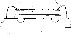
In Fig. 1, following structural element has been embedded in the insulative resin 10.That is, imbedded weld zone 11A, with the distribution 11B of this weld zone 11A one, with the external connecting electrode 11C of the integrally formed other end that is arranged on this distribution 11B of distribution 11B.In addition, also imbedded and be arranged on the electrode 11D that the heat release in the zone that is surrounded by this conductive pattern 11A~11C uses and be arranged on semiconductor element 12 on the electrode 11D that this heat release uses.The electrode 11D that semiconductor element 12 is used by insulating properties adhesive substance AD and above-mentioned heat release fixes, and in Figure 1A, dots.
In addition, the welding electrode 13 of semiconductor element 12 and weld zone 11A are electrically connected by metal fine 14.
In addition, etching is carried out with non-anisotropy in the side of above-mentioned weld zone 11A, here, form by wet corrosion, so, have warp architecture, by this warp architecture generation braking effect.
Electrode 11D, the insulating properties felting cell AD that this structure is used by semiconductor element 12, a plurality of conductive pattern 11A~11C, heat release and 4 kinds of materials such as insulative resin 10 that they are imbedded wherein constitute.In addition, in the configuring area of semiconductor element 12, form above-mentioned insulating properties felting cell AD on conductive pattern 11B~11D and between them, above-mentioned insulating properties felting cell AD particularly is set in the splitter box that forms by etching, and exposes its back side.In addition, comprising above-mentioned these materials all seals with insulative resin 10.And, support above-mentioned weld zone 11A and semiconductor element 12 by insulative resin 10.
As the insulating properties felting cell, the insulating trip of the bonding agent that forms by insulating material, cementability preferably.In addition, by the described manufacture method in back as can be known, preferably can paste on the entire wafer and can utilize photoetching process to scribe the material of figure.In addition, as insulative resin, can use thermoplastic resins such as thermosetting resin, polyimide resin, sulfuration polyphenyl such as epoxy resin.In addition, if insulative resin be to use mold cured resin, dip mold, can be coated with and the resin that is covered, then all resins just all can adopt.In addition, as conductive pattern 11A~11D, can use with Cu as the conductive foil of main material, with conductive foil or Fe-Ni alloy, the layer-collecting body of Al-Cu and the layer-collecting body of Al-Cu-Al etc. of Al as main material.Certainly, also can be other electric conducting material, the electric conducting material that preferably can carry out etched electric conducting material and evaporate particularly by laser radiation.In addition, if when considering the formation of etching partially property, plating and thermal stress, preferably with the electric conducting material that is main material by the rolling Cu that forms.
In the present invention, because insulative resin 10 and insulating properties felting cell AD also be filled in the above-mentioned splitter box, so, have the feature that can prevent that conductive pattern from coming off.In addition,, carry out non-anisotropic etching, make the side of weld zone 11A become warp architecture, also can produce braking effect by adopting dry corrosion or wet corrosion as etching.As a result, can realize the structure that conductive pattern 11A~11D can not deviate from from insulative resin 10.
And expose from the back side of assembly at the back side of conductive pattern 11A~11D.Therefore, the back side of the electrode 11D that heat release is used is fixed with the electrode on the assembling substrate, utilizes this structure, can be to the electrode heat release on the assembling substrate from the heat that semiconductor element 12 takes place, thereby the temperature that can prevent semiconductor element 12 rises, and increases the drive current of semiconductor element 12.In addition, the electrode 11C that uses of heat release also can be electrically connected with semiconductor element 12.
This semiconductor device is supported conductive pattern 11A~11D by the insulative resin 10 as potting resin, so, do not need support substrate.This structure is a feature of the present invention.As technology department's branch explanation is formerly arranged, conduction route support substrate (soft board, printed circuit board (PCB) or the ceramic wafer) support of the semiconductor device that has earlier, or by the lead frame support, so, added original and unwanted structure.But this circuit arrangement is made of required minimal structural element, does not need support substrate, become the device of slim, light weight and do not need fee of material, so, have cheap feature.
In addition, expose conductive pattern 11A~11D at the back side of assembly.If when scolders such as for example scolding tin are layed onto this zone, because the area of the electrode 11D that heat release is used is big, so scolder will soak into a thick layer of.Therefore, when being fixed on the assembling substrate, the wetting at the external connecting electrode 11C back side is less than on the electrode of assembling on the substrate, thereby will come in contact bad phenomenon.
In order to address this problem, form insulating coating film 16 at the back side of semiconductor device 15.Represent the external connecting electrode 11C, the electrode 11D that heat release is used that expose from insulating coating film 16 at the O of the dotted line shown in Figure 1A.That is, covered by insulating coating film 16 beyond this O, the size of O part is actually identical size, so the thickness of the scolder that forms at this place is actually identical.This behind the solder printing with also be the same after anti-fluid welding connects.In addition, we can say it also is the same for conducting resinls such as Ag, Au, Ag-Pd.Utilize this structure, can also suppress poor electric contact.In addition, consider the exothermicity of semiconductor element, the exposed division 17 of the electrode 11D that heat release is used can form and expose the big size of size than external connecting electrode 11C.In addition, because external connecting electrode 11C in fact all is identical size, so external connecting electrode 11C exposes at Zone Full, and the part at the back side of the electrode 11D that heat release is used also can be exposed with practically identical size from insulating coating film 16.
In addition, by insulating coating film 16 being set, can making the back side that the distribution that is arranged on the assembling substrate extends to this semiconductor device.Usually, be arranged on the distribution configuration round in the fixed area of above-mentioned semiconductor device on the assembling substrate, still,, just can be configured round by forming above-mentioned insulating coating film 16.And, because insulative resin 10 and insulating properties felting cell AD are more outstanding than conductive pattern, so, can between distribution that assembles substrate-side and conductive pattern, form the gap, thereby can prevent short circuit phenomenon.
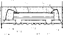
The manufacture method of the semiconductor device 15 that 2. manufacture methods of embodiment are presentation graphs 1, Fig. 2~Fig. 6 is the profile corresponding with the A-A line of Figure 1A.
Prepare conductive foil 20 at first, as shown in Figure 2.Thickness preferably is about 10 μ m~300 μ m,, adopts the rolled copper foil of 70 μ m here.Then, on the surface of this conductive foil 20,, form conduction by overlay film 21 or photoresist as the etch resistant mask.This figure is the identical figure of using with weld zone 11A, distribution 11B, external connecting electrode 11C, the heat release of Figure 1A of electrode 11D.In addition, when adopting photoresist to replace conduction,, form conductions such as Au, Ag, Pd or Ni in corresponding with the weld zone at least part by overlay film in the lower floor of photoresist by overlay film 21.This is provided with in order to weld.(more than, referring to Fig. 2)
Then, conductive foil 20 is etched partially by overlay film 21 or photoresist by above-mentioned conduction.As long as etched depth is shallow just more passable than the thickness of conductive foil 20.Etched depth is shallow more, can form Micropicture more.
And by etching partially, conductive pattern 11A~11D is rendered as convex on the surface of conductive foil 20.As previously mentioned, adopt here with the Cu paper tinsel that is main material by the rolling Cu that forms as conductive foil 20.But, also can be the conductive foil that constitutes by Al, the conductive foil, the layer-collecting body of Cu-Al and the layer-collecting body of Al-Cu-Al that constitute by the Fe-Ni alloy.Particularly the layer-collecting body of Al-Cu-Al can prevent the perk that the difference owing to thermal coefficient of expansion takes place.
And, form insulating properties felting cell AD in the part of the dotted line correspondence of Fig. 1.This insulating properties felting cell AD is arranged on the splitter box of electrode 11D that heat release uses and external connecting electrode 11C, electrode 11D that heat release is used and the splitter box between the distribution 11B and they.(more than, referring to Fig. 3)
Then, semiconductor element 12 is fixed in the zone that is provided with insulating properties felting cell AD, the welding electrode 13 of semiconductor element 12 is electrically connected with weld zone 11A.Among the figure, semiconductor element 12 assembling that faces up, so, as linkage unit, adopt metal fine 14.
In welding, because weld zone 11A and conductive foil 20 are one, and the back side of conductive foil 20 is planes, so, be that face contacts with the table top of welding robot.Therefore, if conductive foil 20 is completely fixed on the welding bench, just the position deviation of weld zone 11A can not take place, thereby can make welding energy effectively to metal fine 14 and weld zone 11A conduction.Therefore, can improve the constant intensity of metal fine 14 during connection.Fixing of welding bench can be realized by a plurality of vacuum attractions hole for example is set on whole table top.In addition, also can be from top extruding conductive foil 20.
In addition, do not adopt support substrate just can assemble semiconductor element, thereby the level configurations of semiconductor element 12 can be got very low.Therefore, can make the thickness attenuation of the profile of the described assembly in back.(more than, referring to Fig. 4)
And, form insulative resin 10, in order to cover by etching partially conductive pattern 11A~11D, semiconductor element 12 and the metal fine 14 that forms.As insulative resin, can be any in thermoplastic resin and the thermosetting resin.
In addition, can realize by transfer molding, injection molding, infusion process or rubbing method.As resin material, can utilize transfer molding to realize thermosetting resins such as epoxy resin, utilize the injection molding can realize thermoplastic resins such as liquid crystal polymer, sulfuration polyphenyl.
In the present embodiment, the thickness of insulative resin is adjusted into about 100 μ m that begin to be covered from the top of metal fine 14 thereon.Consider the intensity of semiconductor device, this thickness can thickly approach.
Inject at resin, conductive pattern 11A~11D and laminar conduction thin 20 becomes one, so, as long as conduction approaches 20 not dislocation, the position deviation of conductive pattern 11A~11D just can not take place fully.
More than, be that conductive pattern 11A~11D and the semiconductor element 12 that forms as lug boss is embedded in the insulative resin 10, the conductive foil 20 lower than lug boss exposes overleaf.(more than, referring to Fig. 5)
Then, remove the conductive foil 20 that exposes at the back side of above-mentioned insulative resin 10, thereby conductive pattern 11A~11D is separated singly.
This separation circuit can be considered various methods, can remove the back side by etching and separate, and also can separate by grinding or cutting process.In addition, also can two kinds of methods all adopt.For example, when exposing insulative resin 10 by cutting, the cutting slag of conductive foil 20 and extend to thinly the outside metallic bur power will invade among insulative resin 10 or the insulating properties felting cell AD.Therefore, if by etching weld zone 11A is separated, the metal of conductive foil 20 just can not invade insulative resin 10 between conductive pattern 11A~11D or the surface of insulating properties felting cell AD.Like this, just, can prevent the short circuit between the conductive pattern 11A~11D at fine interval.(more than, referring to Fig. 5).
In addition, form in 1 unit that becomes semiconductor device 15 when a plurality of, after this separation circuit, should increase cutting action.
Here, adopt cutter sweep to separate singly, still, also can utilize cut apart, punching press or cutting method.
Here, the last formation of the conductive pattern 11A~11D insulating coating film 16 that exposes overleaf after the separation is scribed figure, in order to expose the part of being represented by the dashed circle of Figure 1A on insulating coating film 16.And, after this, obtain semiconductor device cutting by the part shown in the arrow.
Scolding tin 21 can form before cutting or after the cutting.
Utilize above-mentioned manufacture method, can realize conductive pattern and semiconductor component-buried light, thin and short and small assembly in insulative resin.
Fig. 3~insulating properties felting cell AD shown in Figure 4 also can paste mutually in the stage of the wafer before semiconductor element 12 is separated into one by one.That is,, form laminar bonding agent, when cutting, if wafer is cut off, with regard to the operation that on conductive foil 20, forms insulating properties felting cell AD shown in the operation that does not need Fig. 3 with thin slice at chip back surface in the stage of wafer.
Fig. 7 is the figure that is illustrated in the conductive pattern that forms on the conductive foil 20.Here, vertically form 4 unit, laterally forming 8 unit, becoming the shape of lead frame.
30A, 30B are the signs of the position of expression line of cut, and cutting blade is configured between these two lines, thereby is separated into semiconductor device one by one.In addition, the 31, the 32nd, witness marker.The bight of representing chip by the line of the L type shown in 33A, the 33B.The bight configuration of chip also is fixed to this bight.
Below, the effect of utilizing above-mentioned manufacture method to take place is described.
At first, the 1st, conductive pattern is carried out and etches partially, and become one with conductive foil and be supported, so, can remove in the past as supporting to use employed substrate.
The 2nd, on conductive foil, form by etching partially the weld zone that becomes lug boss, so, can realize the miniaturization of weld zone.Therefore, can reduced width and at interval, thus can form the littler assembly of planar dimension.
The 3rd, because constitute by conductive pattern, semiconductor element, connection material and encapsulating material, so, can constitute by required minimal key element, unnecessary material can be removed as far as possible, thereby the slim semiconductor device that reduces cost significantly can be realized.
The 4th, the weld zone forms lug boss by etching partially, after encapsulation, separate singly, so, do not need tie-rod and hanging lead.Therefore, do not need to form tie-rod (hanging lead) and shearing tie-rod (hanging lead) in the present invention fully.
The 5th, after the conductive pattern that becomes lug boss is embedded in the insulative resin, remove conductive foil from the back side of insulative resin, isolate conductive pattern, so, can eliminate the resin fin of generation between lead-in wire and lead-in wire like that of lead frame in the past.
The 6th, the electrode that semiconductor element is used by insulating properties felting cell and heat release is fixed, and the electrode that this heat release is used exposes from the back side, so, can be effectively the heat that this semiconductor device takes place be emitted from the back side of this semiconductor device.In addition, by fillers such as Si oxide-film or aluminium oxide are sneaked in the insulating properties felting cell, can further improve its exothermicity.In addition, if the size of filler is unified, just could make the semiconductor element 12 and the gap of conductive pattern keep certain.
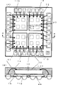
Fig. 8 represents this semiconductor device 42.Fig. 8 A is its plane graph, and Fig. 8 B is the profile along the A-A line.
In Fig. 1, distribution 11B, external connecting electrode 11C and weld zone 11A form, and still, here, the back side of weld zone 11A becomes external connecting electrode.
In addition, because the back side of weld zone 11A is rectangle, so the figure that exposes from insulating coating film 16 also forms the figure identical with above-mentioned rectangle.In addition, consider the cementability of insulating properties felting cell AD, form ditch 43, be divided into a plurality of in order to the electrode 11D that heat release is used.
According to the above description as can be known, in the present invention, do not adopt support substrate, the conductive pattern that forms island also can will be embedded in insulating properties felting cell and the insulative resin and constitutes by having certain thickness conductive foil.In addition, expose owing to be positioned at the electrode that the heat release at the back side of semiconductor element uses, so, the exothermicity of semiconductor element can be improved.And, owing to do not adopt support substrate, so, can realize slim and assembly light weight.
In addition, constitute by required minimal structural elements such as conductive pattern, semiconductor element and insulative resins, thereby become the circuit arrangement that does not have the wasting of resources.Therefore, till finishing assembly, do not have unnecessary inscape, thereby can realize the semiconductor device that can reduce cost significantly.
Claims (11)
1. semiconductor device is characterized in that: the heat release electrode in the configuring area that have the pad that is provided with accordingly with the welding electrode of semiconductor element, is arranged on above-mentioned semiconductor element, cover above-mentioned heat release electrode and be filled to insulating properties felting cell in the ditch that is arranged between above-mentioned heat release electrode and the above-mentioned pad, be fixed on the above-mentioned semiconductor element that is electrically connected with above-mentioned pad on the above-mentioned insulating properties felting cell and the back side of exposing above-mentioned pad and above-mentioned insulating properties felting cell and encapsulate the insulative resin of above-mentioned semiconductor element integratedly.
2. by the described semiconductor device of claim 1, it is characterized in that: above-mentioned insulating properties felting cell is adhesive sheet or bonding agent.
3. by the described semiconductor device of claim 1, it is characterized in that: above-mentioned semiconductor element assembles in supine mode, and above-mentioned pad is connected with metal fine with above-mentioned welding electrode.
4. a semiconductor device is characterized in that: have a plurality of weld zones that surround a zone and be provided with, the external connecting electrode that extends integratedly with above-mentioned weld zone, be arranged on the heat release electrode in the above-mentioned zone, cover above-mentioned heat release electrode and be filled to insulating properties felting cell in the ditch that is arranged between above-mentioned heat release electrode and the above-mentioned weld zone, the fixing semiconductor element by above-mentioned insulating properties felting cell, the metal fine that welding electrode on the above-mentioned semiconductor element is connected with above-mentioned weld zone, be layed onto above-mentioned semiconductor element, above-mentioned weld zone, above-mentioned heat release electrode, on said external connection electrode and the above-mentioned metal fine and the back side of exposing the said external connection electrode, the insulative resin at the back side of the back side of above-mentioned heat release electrode and above-mentioned insulating properties felting cell.
5. semiconductor device, it is characterized in that: have a plurality of pads that surround a zone and be provided with, be arranged on the heat release electrode in the above-mentioned zone, cover above-mentioned heat release electrode and be filled to insulating properties felting cell in the ditch that is arranged between above-mentioned heat release electrode and the above-mentioned pad, the fixing semiconductor element by above-mentioned insulating properties felting cell, the linkage unit that welding electrode on the above-mentioned semiconductor element is connected with above-mentioned pad, be layed onto above-mentioned semiconductor element, on above-mentioned weld zone and the above-mentioned linkage unit and expose the back side of above-mentioned weld zone and the insulative resin of above-mentioned insulating properties felting cell, with the back side of above-mentioned weld zone as external connecting electrode.
6. by the described semiconductor device of claim 5, it is characterized in that: above-mentioned linkage unit is a metal fine.
7. by the described semiconductor device of claim 1, it is characterized in that: the side of above-mentioned pad or above-mentioned electrode is a warp architecture.
8. the manufacture method of a semiconductor device, it is characterized in that: prepare conductive foil, and it is etched partially so that conductive pattern forms convex, the insulating properties felting cell is set in order to fill by the above-mentioned splitter box that forms that etches partially, be electrically connected with above-mentioned conductive pattern and by the fixing semiconductor element of above-mentioned insulating properties felting cell, insulative resin is set in order to encapsulate above-mentioned semiconductor element and above-mentioned conductive pattern on above-mentioned conductive foil, the back side of exposing above-mentioned insulating properties felting cell is removed the back side of above-mentioned conductive foil and is isolated conductive pattern.
9. the manufacture method of a semiconductor device, it is characterized in that: prepare conductive foil, and to its etch partially so that at least the conductive pattern that constitutes by pad and heat release electrode form convex, setting is layed onto on the above-mentioned heat release electrode in order to be filled into the insulating properties felting cell in the splitter box adjacent with this electrode, be electrically connected with above-mentioned pad and semiconductor element be fixed on the above-mentioned heat release electrode by above-mentioned insulating properties felting cell, insulative resin is set in order to encapsulate above-mentioned semiconductor element and above-mentioned pad on above-mentioned conductive foil, the back side of exposing above-mentioned insulating properties felting cell is removed the back side of above-mentioned conductive foil and is isolated above-mentioned conductive pattern.
10. the manufacture method of a semiconductor device, it is characterized in that: prepare conductive foil, and it is etched partially, form convex so that will become the zone of conductive pattern, setting is filled into the insulating properties felting cell that etches partially in the splitter box that forms by above-mentioned, be electrically connected with above-mentioned conductive pattern and semiconductor element fixed by above-mentioned insulating properties felting cell, insulative resin is set in order to encapsulate above-mentioned semiconductor element on above-mentioned conductive foil, above-mentioned conductive pattern, the back side of exposing above-mentioned insulating properties felting cell is removed the back side of above-mentioned conductive foil and is isolated above-mentioned conductive pattern.
11. the manufacture method of a semiconductor device, it is characterized in that: prepare conductive foil, and it is etched partially, form convex so that will become the zone of the conductive pattern that constitutes pad and electrode, setting is layed onto on the above-mentioned electrode in order to be filled into the insulating properties felting cell in the splitter box adjacent with this electrode, be electrically connected with above-mentioned pad and semiconductor element be fixed on the above-mentioned electrode by above-mentioned insulating properties felting cell, insulative resin is set in order to encapsulate above-mentioned semiconductor element and above-mentioned pad on above-mentioned conductive foil, the back side of exposing above-mentioned insulating properties felting cell is removed the back side of above-mentioned conductive foil and is isolated above-mentioned conductive pattern.
Applications Claiming Priority (2)
| Application Number | Priority Date | Filing Date | Title |
|---|---|---|---|
| JP269467/00 | 2000-09-06 | ||
| JP2000269467 | 2000-09-06 |
Publications (2)
| Publication Number | Publication Date |
|---|---|
| CN1341962A CN1341962A (en) | 2002-03-27 |
| CN1265451C true CN1265451C (en) | 2006-07-19 |
Family
ID=18756068
Family Applications (1)
| Application Number | Title | Priority Date | Filing Date |
|---|---|---|---|
| CNB011045531A Expired - Fee Related CN1265451C (en) | 2000-09-06 | 2001-02-15 | Semiconductor device and manufactoring method thereof |
Country Status (5)
| Country | Link |
|---|---|
| US (2) | US6462418B2 (en) |
| EP (1) | EP1187203A3 (en) |
| KR (1) | KR100407595B1 (en) |
| CN (1) | CN1265451C (en) |
| TW (1) | TW501382B (en) |
Families Citing this family (60)
| Publication number | Priority date | Publication date | Assignee | Title |
|---|---|---|---|---|
| JP3420153B2 (en) * | 2000-01-24 | 2003-06-23 | Necエレクトロニクス株式会社 | Semiconductor device and manufacturing method thereof |
| JP3883784B2 (en) * | 2000-05-24 | 2007-02-21 | 三洋電機株式会社 | Plate-shaped body and method for manufacturing semiconductor device |
| JP3609737B2 (en) * | 2001-03-22 | 2005-01-12 | 三洋電機株式会社 | Circuit device manufacturing method |
| TW538658B (en) * | 2001-08-27 | 2003-06-21 | Sanyo Electric Co | Manufacturing method for circuit device |
| DE10148120B4 (en) * | 2001-09-28 | 2007-02-01 | Infineon Technologies Ag | Electronic components with semiconductor chips and a system carrier with component positions and method for producing a system carrier |
| CN1303852C (en) * | 2002-06-12 | 2007-03-07 | 威盛电子股份有限公司 | Radiating structure of lead frame package and method for improving radiating performance of the same package |
| JP2004179253A (en) * | 2002-11-25 | 2004-06-24 | Nec Semiconductors Kyushu Ltd | Semiconductor device and manufacturing method therefor |
| JP2004186362A (en) * | 2002-12-03 | 2004-07-02 | Sanyo Electric Co Ltd | Circuit device |
| SG119185A1 (en) | 2003-05-06 | 2006-02-28 | Micron Technology Inc | Method for packaging circuits and packaged circuits |
| JP2005109225A (en) * | 2003-09-30 | 2005-04-21 | Sanyo Electric Co Ltd | Circuit device |
| US7488565B2 (en) * | 2003-10-01 | 2009-02-10 | Chevron U.S.A. Inc. | Photoresist compositions comprising diamondoid derivatives |
| JP4446772B2 (en) * | 2004-03-24 | 2010-04-07 | 三洋電機株式会社 | Circuit device and manufacturing method thereof |
| JP4489485B2 (en) | 2004-03-31 | 2010-06-23 | 株式会社ルネサステクノロジ | Semiconductor device |
| WO2006132151A1 (en) * | 2005-06-06 | 2006-12-14 | Rohm Co., Ltd. | Interposer and semiconductor device |
| JP5081578B2 (en) | 2007-10-25 | 2012-11-28 | ローム株式会社 | Resin-sealed semiconductor device |
| US7727813B2 (en) * | 2007-11-26 | 2010-06-01 | Infineon Technologies Ag | Method for making a device including placing a semiconductor chip on a substrate |
| WO2011153298A1 (en) | 2010-06-03 | 2011-12-08 | Hsio Technologies, Llc | Electrical connector insulator housing |
| WO2014011232A1 (en) | 2012-07-12 | 2014-01-16 | Hsio Technologies, Llc | Semiconductor socket with direct selective metalization |
| WO2011139619A1 (en) | 2010-04-26 | 2011-11-10 | Hsio Technologies, Llc | Semiconductor device package adapter |
| US9276336B2 (en) | 2009-05-28 | 2016-03-01 | Hsio Technologies, Llc | Metalized pad to electrical contact interface |
| US8955215B2 (en) | 2009-05-28 | 2015-02-17 | Hsio Technologies, Llc | High performance surface mount electrical interconnect |
| WO2010141313A1 (en) | 2009-06-02 | 2010-12-09 | Hsio Technologies, Llc | Compliant printed circuit socket diagnostic tool |
| US9930775B2 (en) | 2009-06-02 | 2018-03-27 | Hsio Technologies, Llc | Copper pillar full metal via electrical circuit structure |
| US9613841B2 (en) | 2009-06-02 | 2017-04-04 | Hsio Technologies, Llc | Area array semiconductor device package interconnect structure with optional package-to-package or flexible circuit to package connection |
| US8988093B2 (en) | 2009-06-02 | 2015-03-24 | Hsio Technologies, Llc | Bumped semiconductor wafer or die level electrical interconnect |
| US9136196B2 (en) | 2009-06-02 | 2015-09-15 | Hsio Technologies, Llc | Compliant printed circuit wafer level semiconductor package |
| WO2010141266A1 (en) | 2009-06-02 | 2010-12-09 | Hsio Technologies, Llc | Compliant printed circuit peripheral lead semiconductor package |
| US9318862B2 (en) | 2009-06-02 | 2016-04-19 | Hsio Technologies, Llc | Method of making an electronic interconnect |
| US8912812B2 (en) | 2009-06-02 | 2014-12-16 | Hsio Technologies, Llc | Compliant printed circuit wafer probe diagnostic tool |
| WO2010141295A1 (en) | 2009-06-02 | 2010-12-09 | Hsio Technologies, Llc | Compliant printed flexible circuit |
| US8987886B2 (en) | 2009-06-02 | 2015-03-24 | Hsio Technologies, Llc | Copper pillar full metal via electrical circuit structure |
| WO2012061008A1 (en) | 2010-10-25 | 2012-05-10 | Hsio Technologies, Llc | High performance electrical circuit structure |
| WO2010141296A1 (en) | 2009-06-02 | 2010-12-09 | Hsio Technologies, Llc | Compliant printed circuit semiconductor package |
| US9196980B2 (en) | 2009-06-02 | 2015-11-24 | Hsio Technologies, Llc | High performance surface mount electrical interconnect with external biased normal force loading |
| US8525346B2 (en) | 2009-06-02 | 2013-09-03 | Hsio Technologies, Llc | Compliant conductive nano-particle electrical interconnect |
| WO2012078493A1 (en) | 2010-12-06 | 2012-06-14 | Hsio Technologies, Llc | Electrical interconnect ic device socket |
| US9054097B2 (en) | 2009-06-02 | 2015-06-09 | Hsio Technologies, Llc | Compliant printed circuit area array semiconductor device package |
| US9093767B2 (en) | 2009-06-02 | 2015-07-28 | Hsio Technologies, Llc | High performance surface mount electrical interconnect |
| US8970031B2 (en) * | 2009-06-16 | 2015-03-03 | Hsio Technologies, Llc | Semiconductor die terminal |
| US8610265B2 (en) | 2009-06-02 | 2013-12-17 | Hsio Technologies, Llc | Compliant core peripheral lead semiconductor test socket |
| WO2010141303A1 (en) | 2009-06-02 | 2010-12-09 | Hsio Technologies, Llc | Resilient conductive electrical interconnect |
| US9699906B2 (en) | 2009-06-02 | 2017-07-04 | Hsio Technologies, Llc | Hybrid printed circuit assembly with low density main core and embedded high density circuit regions |
| WO2010141318A1 (en) | 2009-06-02 | 2010-12-09 | Hsio Technologies, Llc | Compliant printed circuit peripheral lead semiconductor test socket |
| US9277654B2 (en) | 2009-06-02 | 2016-03-01 | Hsio Technologies, Llc | Composite polymer-metal electrical contacts |
| US9603249B2 (en) | 2009-06-02 | 2017-03-21 | Hsio Technologies, Llc | Direct metalization of electrical circuit structures |
| WO2011002712A1 (en) | 2009-06-29 | 2011-01-06 | Hsio Technologies, Llc | Singulated semiconductor device separable electrical interconnect |
| US9276339B2 (en) | 2009-06-02 | 2016-03-01 | Hsio Technologies, Llc | Electrical interconnect IC device socket |
| US8803539B2 (en) | 2009-06-03 | 2014-08-12 | Hsio Technologies, Llc | Compliant wafer level probe assembly |
| WO2010147782A1 (en) | 2009-06-16 | 2010-12-23 | Hsio Technologies, Llc | Simulated wirebond semiconductor package |
| US9320144B2 (en) | 2009-06-17 | 2016-04-19 | Hsio Technologies, Llc | Method of forming a semiconductor socket |
| US8981809B2 (en) | 2009-06-29 | 2015-03-17 | Hsio Technologies, Llc | Compliant printed circuit semiconductor tester interface |
| US8758067B2 (en) | 2010-06-03 | 2014-06-24 | Hsio Technologies, Llc | Selective metalization of electrical connector or socket housing |
| US9350093B2 (en) | 2010-06-03 | 2016-05-24 | Hsio Technologies, Llc | Selective metalization of electrical connector or socket housing |
| US10159154B2 (en) | 2010-06-03 | 2018-12-18 | Hsio Technologies, Llc | Fusion bonded liquid crystal polymer circuit structure |
| US9689897B2 (en) | 2010-06-03 | 2017-06-27 | Hsio Technologies, Llc | Performance enhanced semiconductor socket |
| US9761520B2 (en) | 2012-07-10 | 2017-09-12 | Hsio Technologies, Llc | Method of making an electrical connector having electrodeposited terminals |
| US10506722B2 (en) | 2013-07-11 | 2019-12-10 | Hsio Technologies, Llc | Fusion bonded liquid crystal polymer electrical circuit structure |
| US10667410B2 (en) | 2013-07-11 | 2020-05-26 | Hsio Technologies, Llc | Method of making a fusion bonded circuit structure |
| US9559447B2 (en) | 2015-03-18 | 2017-01-31 | Hsio Technologies, Llc | Mechanical contact retention within an electrical connector |
| KR101944783B1 (en) | 2017-01-16 | 2019-04-18 | 일진머티리얼즈 주식회사 | Copper foil attached to the carrier foil |
Family Cites Families (8)
| Publication number | Priority date | Publication date | Assignee | Title |
|---|---|---|---|---|
| EP1213756A3 (en) | 1994-03-18 | 2005-05-25 | Hitachi Chemical Co., Ltd. | Fabrication process of semiconductor package and semiconductor package |
| JP3509274B2 (en) * | 1994-07-13 | 2004-03-22 | セイコーエプソン株式会社 | Resin-sealed semiconductor device and method of manufacturing the same |
| US6001671A (en) * | 1996-04-18 | 1999-12-14 | Tessera, Inc. | Methods for manufacturing a semiconductor package having a sacrificial layer |
| JPH09312355A (en) * | 1996-05-21 | 1997-12-02 | Shinko Electric Ind Co Ltd | Semiconductor device and its manufacture |
| US6201292B1 (en) * | 1997-04-02 | 2001-03-13 | Dai Nippon Insatsu Kabushiki Kaisha | Resin-sealed semiconductor device, circuit member used therefor |
| JPH10335566A (en) * | 1997-04-02 | 1998-12-18 | Dainippon Printing Co Ltd | Resin-sealed semiconductor device and circuit member used therein, and manufacture of resin-sealed semiconductor device |
| JP3521758B2 (en) * | 1997-10-28 | 2004-04-19 | セイコーエプソン株式会社 | Method for manufacturing semiconductor device |
| JPH11195742A (en) * | 1998-01-05 | 1999-07-21 | Matsushita Electron Corp | Semiconductor device, manufacture thereof, and led frame therefor |
-
2001
- 2001-02-15 CN CNB011045531A patent/CN1265451C/en not_active Expired - Fee Related
- 2001-02-16 TW TW90103573A patent/TW501382B/en not_active IP Right Cessation
- 2001-02-24 KR KR10-2001-0009507A patent/KR100407595B1/en not_active IP Right Cessation
- 2001-03-16 US US09/809,849 patent/US6462418B2/en not_active Expired - Lifetime
- 2001-03-20 EP EP20010302549 patent/EP1187203A3/en not_active Withdrawn
-
2002
- 2002-09-06 US US10/236,502 patent/US6596564B2/en not_active Expired - Fee Related
Also Published As
| Publication number | Publication date |
|---|---|
| KR100407595B1 (en) | 2003-12-01 |
| TW501382B (en) | 2002-09-01 |
| US6596564B2 (en) | 2003-07-22 |
| CN1341962A (en) | 2002-03-27 |
| US20030011065A1 (en) | 2003-01-16 |
| KR20020020169A (en) | 2002-03-14 |
| US20020027290A1 (en) | 2002-03-07 |
| EP1187203A3 (en) | 2004-04-14 |
| US6462418B2 (en) | 2002-10-08 |
| EP1187203A2 (en) | 2002-03-13 |
Similar Documents
| Publication | Publication Date | Title |
|---|---|---|
| CN1265451C (en) | Semiconductor device and manufactoring method thereof | |
| JP5442368B2 (en) | IC chip package with direct lead wire | |
| US6909178B2 (en) | Semiconductor device and method of manufacturing the same | |
| US7256479B2 (en) | Method to manufacture a universal footprint for a package with exposed chip | |
| KR960003766B1 (en) | Plastic pin grid array package | |
| CN1177358C (en) | Semiconductor device chip scale surface assembling and packaging, and mfg. method therefor | |
| JP2809115B2 (en) | Semiconductor device and manufacturing method thereof | |
| CN1309283C (en) | Manufacturing method of circuit device | |
| US20070258215A1 (en) | High-power ball grid array package, heat spreader used in the bga package and method for manufacturing the same | |
| CN1266765C (en) | Semiconductor device and manufacturing method thereof | |
| JPH07321250A (en) | Ball lattice array integrated circuit package with heat conductor | |
| CN1571151A (en) | Double gauge lead frame | |
| CN103367300A (en) | Lead frame, semiconductor device, and method for manufacturing lead frame | |
| KR100606295B1 (en) | Circuit module | |
| CN1591841A (en) | Tape circuit substrate and semiconductor chip package using the same | |
| CN1186807C (en) | Method for producing circuit device | |
| JP5447928B2 (en) | Mounting substrate and method of manufacturing thin light emitting device using the same | |
| JP2001085603A (en) | Semiconductor device | |
| JP2009010213A (en) | Hybrid integrated circuit device | |
| CN1577815A (en) | High-density chip scale package and method of manufacturing the same | |
| JPH09326450A (en) | Semiconductor device and its manufacture | |
| JPH06132441A (en) | Resin-sealed semiconductor device and manufacture thereof | |
| KR101008534B1 (en) | Power semiconductor mudule package and method for fabricating the same | |
| JP2002270711A (en) | Wiring board for semiconductor device and manufacturing method therefor | |
| JPH08321565A (en) | Semiconductor device |
Legal Events
| Date | Code | Title | Description |
|---|---|---|---|
| C06 | Publication | ||
| PB01 | Publication | ||
| C10 | Entry into substantive examination | ||
| SE01 | Entry into force of request for substantive examination | ||
| C10 | Entry into substantive examination | ||
| SE01 | Entry into force of request for substantive examination | ||
| C14 | Grant of patent or utility model | ||
| GR01 | Patent grant | ||
| C17 | Cessation of patent right | ||
| CF01 | Termination of patent right due to non-payment of annual fee |
Granted publication date: 20060719 Termination date: 20140215 |