CN1224862C - Electrochemical pixel device - Google Patents
Electrochemical pixel device Download PDFInfo
- Publication number
- CN1224862C CN1224862C CNB028061276A CN02806127A CN1224862C CN 1224862 C CN1224862 C CN 1224862C CN B028061276 A CNB028061276 A CN B028061276A CN 02806127 A CN02806127 A CN 02806127A CN 1224862 C CN1224862 C CN 1224862C
- Authority
- CN
- China
- Prior art keywords
- electrochemical
- electrochromic
- electrode
- pixel device
- galvanochemistry
- Prior art date
- Legal status (The legal status is an assumption and is not a legal conclusion. Google has not performed a legal analysis and makes no representation as to the accuracy of the status listed.)
- Expired - Fee Related
Links
- 239000000463 material Substances 0.000 claims abstract description 111
- 239000003792 electrolyte Substances 0.000 claims abstract description 72
- 238000000034 method Methods 0.000 claims abstract description 38
- 239000011368 organic material Substances 0.000 claims abstract description 26
- 238000007254 oxidation reaction Methods 0.000 claims abstract description 19
- 230000003647 oxidation Effects 0.000 claims abstract description 16
- 239000011159 matrix material Substances 0.000 claims description 42
- YTPLMLYBLZKORZ-UHFFFAOYSA-N Thiophene Chemical compound C=1C=CSC=1 YTPLMLYBLZKORZ-UHFFFAOYSA-N 0.000 claims description 40
- 239000000126 substance Substances 0.000 claims description 32
- 229920000642 polymer Polymers 0.000 claims description 22
- 241000790917 Dioxys <bee> Species 0.000 claims description 20
- 229930192474 thiophene Natural products 0.000 claims description 20
- 229920001467 poly(styrenesulfonates) Polymers 0.000 claims description 15
- 241001597008 Nomeidae Species 0.000 claims description 12
- 238000005516 engineering process Methods 0.000 claims description 11
- -1 polyisothianaphthene Polymers 0.000 claims description 11
- 230000005611 electricity Effects 0.000 claims description 10
- 239000000123 paper Substances 0.000 claims description 10
- 239000003795 chemical substances by application Substances 0.000 claims description 9
- 230000008021 deposition Effects 0.000 claims description 6
- 229920000159 gelatin Polymers 0.000 claims description 6
- 235000019322 gelatine Nutrition 0.000 claims description 6
- 238000006116 polymerization reaction Methods 0.000 claims description 6
- 229920000123 polythiophene Polymers 0.000 claims description 6
- 238000007639 printing Methods 0.000 claims description 6
- 150000003839 salts Chemical class 0.000 claims description 6
- 230000015572 biosynthetic process Effects 0.000 claims description 5
- 239000011248 coating agent Substances 0.000 claims description 5
- 238000000576 coating method Methods 0.000 claims description 5
- 150000001875 compounds Chemical class 0.000 claims description 5
- 229920000767 polyaniline Polymers 0.000 claims description 5
- 229920000128 polypyrrole Polymers 0.000 claims description 5
- 239000000758 substrate Substances 0.000 claims description 5
- 108010010803 Gelatin Proteins 0.000 claims description 4
- HGAZMNJKRQFZKS-UHFFFAOYSA-N chloroethene;ethenyl acetate Chemical compound ClC=C.CC(=O)OC=C HGAZMNJKRQFZKS-UHFFFAOYSA-N 0.000 claims description 4
- 239000008273 gelatin Substances 0.000 claims description 4
- 235000011852 gelatine desserts Nutrition 0.000 claims description 4
- 239000004793 Polystyrene Substances 0.000 claims description 3
- 125000003545 alkoxy group Chemical group 0.000 claims description 3
- 229920002223 polystyrene Polymers 0.000 claims description 3
- 239000001828 Gelatine Substances 0.000 claims description 2
- 229920003171 Poly (ethylene oxide) Polymers 0.000 claims description 2
- 239000004743 Polypropylene Substances 0.000 claims description 2
- 229920002125 Sokalan® Polymers 0.000 claims description 2
- 239000002253 acid Substances 0.000 claims description 2
- 239000011521 glass Substances 0.000 claims description 2
- 150000004676 glycans Chemical class 0.000 claims description 2
- 229920003207 poly(ethylene-2,6-naphthalate) Polymers 0.000 claims description 2
- 229920000172 poly(styrenesulfonic acid) Polymers 0.000 claims description 2
- 229920002401 polyacrylamide Polymers 0.000 claims description 2
- 239000004584 polyacrylic acid Substances 0.000 claims description 2
- 229920000515 polycarbonate Polymers 0.000 claims description 2
- 239000004417 polycarbonate Substances 0.000 claims description 2
- 239000011112 polyethylene naphthalate Substances 0.000 claims description 2
- 229920000139 polyethylene terephthalate Polymers 0.000 claims description 2
- 239000005020 polyethylene terephthalate Substances 0.000 claims description 2
- 229920001155 polypropylene Polymers 0.000 claims description 2
- 229920001451 polypropylene glycol Polymers 0.000 claims description 2
- 229920001282 polysaccharide Polymers 0.000 claims description 2
- 239000005017 polysaccharide Substances 0.000 claims description 2
- 229920002635 polyurethane Polymers 0.000 claims description 2
- 239000004814 polyurethane Substances 0.000 claims description 2
- 229920002451 polyvinyl alcohol Polymers 0.000 claims description 2
- 238000003486 chemical etching Methods 0.000 claims 1
- 230000003628 erosive effect Effects 0.000 claims 1
- 238000003032 molecular docking Methods 0.000 claims 1
- 230000008859 change Effects 0.000 abstract description 15
- 238000004519 manufacturing process Methods 0.000 abstract description 8
- 230000008569 process Effects 0.000 abstract description 8
- 239000010410 layer Substances 0.000 description 39
- 238000013461 design Methods 0.000 description 17
- 239000004020 conductor Substances 0.000 description 14
- 229920001940 conductive polymer Polymers 0.000 description 11
- 238000006479 redox reaction Methods 0.000 description 10
- 239000002322 conducting polymer Substances 0.000 description 9
- 238000003487 electrochemical reaction Methods 0.000 description 9
- XEEYBQQBJWHFJM-UHFFFAOYSA-N iron Substances [Fe] XEEYBQQBJWHFJM-UHFFFAOYSA-N 0.000 description 9
- 230000000694 effects Effects 0.000 description 8
- 239000011149 active material Substances 0.000 description 7
- 238000006243 chemical reaction Methods 0.000 description 7
- 150000002500 ions Chemical class 0.000 description 7
- 238000006722 reduction reaction Methods 0.000 description 7
- 239000007787 solid Substances 0.000 description 7
- 239000002800 charge carrier Substances 0.000 description 6
- 230000009467 reduction Effects 0.000 description 6
- 230000008901 benefit Effects 0.000 description 5
- 238000000151 deposition Methods 0.000 description 5
- 239000002245 particle Substances 0.000 description 5
- 230000002441 reversible effect Effects 0.000 description 5
- LFQSCWFLJHTTHZ-UHFFFAOYSA-N Ethanol Chemical compound CCO LFQSCWFLJHTTHZ-UHFFFAOYSA-N 0.000 description 4
- 239000003086 colorant Substances 0.000 description 4
- 230000005684 electric field Effects 0.000 description 4
- 238000005538 encapsulation Methods 0.000 description 4
- 238000002474 experimental method Methods 0.000 description 4
- 239000011888 foil Substances 0.000 description 4
- 229920000447 polyanionic polymer Polymers 0.000 description 4
- 238000012545 processing Methods 0.000 description 4
- 239000004065 semiconductor Substances 0.000 description 4
- 238000013459 approach Methods 0.000 description 3
- 239000013078 crystal Substances 0.000 description 3
- 230000006870 function Effects 0.000 description 3
- 239000007789 gas Substances 0.000 description 3
- 239000000499 gel Substances 0.000 description 3
- 239000011229 interlayer Substances 0.000 description 3
- 239000000203 mixture Substances 0.000 description 3
- 230000010287 polarization Effects 0.000 description 3
- 239000002861 polymer material Substances 0.000 description 3
- 230000005855 radiation Effects 0.000 description 3
- PAYRUJLWNCNPSJ-UHFFFAOYSA-N Aniline Chemical compound NC1=CC=CC=C1 PAYRUJLWNCNPSJ-UHFFFAOYSA-N 0.000 description 2
- CIWBSHSKHKDKBQ-JLAZNSOCSA-N Ascorbic acid Chemical compound OC[C@H](O)[C@H]1OC(=O)C(O)=C1O CIWBSHSKHKDKBQ-JLAZNSOCSA-N 0.000 description 2
- PEDCQBHIVMGVHV-UHFFFAOYSA-N Glycerine Chemical compound OCC(O)CO PEDCQBHIVMGVHV-UHFFFAOYSA-N 0.000 description 2
- TWRXJAOTZQYOKJ-UHFFFAOYSA-L Magnesium chloride Chemical compound [Mg+2].[Cl-].[Cl-] TWRXJAOTZQYOKJ-UHFFFAOYSA-L 0.000 description 2
- CSNNHWWHGAXBCP-UHFFFAOYSA-L Magnesium sulfate Chemical compound [Mg+2].[O-][S+2]([O-])([O-])[O-] CSNNHWWHGAXBCP-UHFFFAOYSA-L 0.000 description 2
- ATJFFYVFTNAWJD-UHFFFAOYSA-N Tin Chemical compound [Sn] ATJFFYVFTNAWJD-UHFFFAOYSA-N 0.000 description 2
- 238000004040 coloring Methods 0.000 description 2
- 230000000295 complement effect Effects 0.000 description 2
- 238000010276 construction Methods 0.000 description 2
- 238000001816 cooling Methods 0.000 description 2
- 238000004042 decolorization Methods 0.000 description 2
- DMBHHRLKUKUOEG-UHFFFAOYSA-N diphenylamine Chemical compound C=1C=CC=CC=1NC1=CC=CC=C1 DMBHHRLKUKUOEG-UHFFFAOYSA-N 0.000 description 2
- 239000006181 electrochemical material Substances 0.000 description 2
- 239000008151 electrolyte solution Substances 0.000 description 2
- 239000008393 encapsulating agent Substances 0.000 description 2
- 230000007613 environmental effect Effects 0.000 description 2
- 229920006335 epoxy glue Polymers 0.000 description 2
- 230000002349 favourable effect Effects 0.000 description 2
- KTWOOEGAPBSYNW-UHFFFAOYSA-N ferrocene Chemical compound [Fe+2].C=1C=C[CH-]C=1.C=1C=C[CH-]C=1 KTWOOEGAPBSYNW-UHFFFAOYSA-N 0.000 description 2
- 230000005669 field effect Effects 0.000 description 2
- DCYOBGZUOMKFPA-UHFFFAOYSA-N iron(2+);iron(3+);octadecacyanide Chemical compound [Fe+2].[Fe+2].[Fe+2].[Fe+3].[Fe+3].[Fe+3].[Fe+3].N#[C-].N#[C-].N#[C-].N#[C-].N#[C-].N#[C-].N#[C-].N#[C-].N#[C-].N#[C-].N#[C-].N#[C-].N#[C-].N#[C-].N#[C-].N#[C-].N#[C-].N#[C-] DCYOBGZUOMKFPA-UHFFFAOYSA-N 0.000 description 2
- 230000002427 irreversible effect Effects 0.000 description 2
- 239000007788 liquid Substances 0.000 description 2
- 239000007791 liquid phase Substances 0.000 description 2
- 229920002521 macromolecule Polymers 0.000 description 2
- 230000003287 optical effect Effects 0.000 description 2
- 239000012071 phase Substances 0.000 description 2
- 229920002959 polymer blend Polymers 0.000 description 2
- 238000002360 preparation method Methods 0.000 description 2
- 238000007790 scraping Methods 0.000 description 2
- 238000000935 solvent evaporation Methods 0.000 description 2
- 238000012360 testing method Methods 0.000 description 2
- XOLBLPGZBRYERU-UHFFFAOYSA-N tin dioxide Chemical compound O=[Sn]=O XOLBLPGZBRYERU-UHFFFAOYSA-N 0.000 description 2
- 229910001887 tin oxide Inorganic materials 0.000 description 2
- 125000000391 vinyl group Chemical group [H]C([*])=C([H])[H] 0.000 description 2
- 229920002554 vinyl polymer Polymers 0.000 description 2
- XLYOFNOQVPJJNP-UHFFFAOYSA-N water Substances O XLYOFNOQVPJJNP-UHFFFAOYSA-N 0.000 description 2
- 241001479434 Agfa Species 0.000 description 1
- ZZZCUOFIHGPKAK-UHFFFAOYSA-N D-erythro-ascorbic acid Natural products OCC1OC(=O)C(O)=C1O ZZZCUOFIHGPKAK-UHFFFAOYSA-N 0.000 description 1
- HMEKVHWROSNWPD-UHFFFAOYSA-N Erioglaucine A Chemical compound [NH4+].[NH4+].C=1C=C(C(=C2C=CC(C=C2)=[N+](CC)CC=2C=C(C=CC=2)S([O-])(=O)=O)C=2C(=CC=CC=2)S([O-])(=O)=O)C=CC=1N(CC)CC1=CC=CC(S([O-])(=O)=O)=C1 HMEKVHWROSNWPD-UHFFFAOYSA-N 0.000 description 1
- PXGOKWXKJXAPGV-UHFFFAOYSA-N Fluorine Chemical compound FF PXGOKWXKJXAPGV-UHFFFAOYSA-N 0.000 description 1
- 229920000663 Hydroxyethyl cellulose Polymers 0.000 description 1
- 239000004354 Hydroxyethyl cellulose Substances 0.000 description 1
- 235000000177 Indigofera tinctoria Nutrition 0.000 description 1
- ISWSIDIOOBJBQZ-UHFFFAOYSA-N Phenol Chemical compound OC1=CC=CC=C1 ISWSIDIOOBJBQZ-UHFFFAOYSA-N 0.000 description 1
- 208000034189 Sclerosis Diseases 0.000 description 1
- 229930003268 Vitamin C Natural products 0.000 description 1
- 239000000654 additive Substances 0.000 description 1
- 230000000996 additive effect Effects 0.000 description 1
- 239000003963 antioxidant agent Substances 0.000 description 1
- 230000003078 antioxidant effect Effects 0.000 description 1
- 235000006708 antioxidants Nutrition 0.000 description 1
- 238000000429 assembly Methods 0.000 description 1
- 230000000712 assembly Effects 0.000 description 1
- QVGXLLKOCUKJST-UHFFFAOYSA-N atomic oxygen Chemical compound [O] QVGXLLKOCUKJST-UHFFFAOYSA-N 0.000 description 1
- 230000009286 beneficial effect Effects 0.000 description 1
- GAWOVNGQYQVFLI-ISLYRVAYSA-N c1cc(OCC)ccc1\N=N\c1ccc(N)cc1N Chemical compound c1cc(OCC)ccc1\N=N\c1ccc(N)cc1N GAWOVNGQYQVFLI-ISLYRVAYSA-N 0.000 description 1
- 239000003153 chemical reaction reagent Substances 0.000 description 1
- 229920000547 conjugated polymer Polymers 0.000 description 1
- 238000007766 curtain coating Methods 0.000 description 1
- 230000001419 dependent effect Effects 0.000 description 1
- 238000003618 dip coating Methods 0.000 description 1
- 239000007772 electrode material Substances 0.000 description 1
- 238000005265 energy consumption Methods 0.000 description 1
- 238000001125 extrusion Methods 0.000 description 1
- 239000004744 fabric Substances 0.000 description 1
- 239000011737 fluorine Substances 0.000 description 1
- 229910052731 fluorine Inorganic materials 0.000 description 1
- 239000012634 fragment Substances 0.000 description 1
- 239000011245 gel electrolyte Substances 0.000 description 1
- 235000011187 glycerol Nutrition 0.000 description 1
- 235000019447 hydroxyethyl cellulose Nutrition 0.000 description 1
- 230000006872 improvement Effects 0.000 description 1
- 229940097275 indigo Drugs 0.000 description 1
- COHYTHOBJLSHDF-UHFFFAOYSA-N indigo powder Natural products N1C2=CC=CC=C2C(=O)C1=C1C(=O)C2=CC=CC=C2N1 COHYTHOBJLSHDF-UHFFFAOYSA-N 0.000 description 1
- 229910052738 indium Inorganic materials 0.000 description 1
- APFVFJFRJDLVQX-UHFFFAOYSA-N indium atom Chemical compound [In] APFVFJFRJDLVQX-UHFFFAOYSA-N 0.000 description 1
- 238000007641 inkjet printing Methods 0.000 description 1
- 238000003475 lamination Methods 0.000 description 1
- 238000011031 large-scale manufacturing process Methods 0.000 description 1
- 239000004816 latex Substances 0.000 description 1
- 229920000126 latex Polymers 0.000 description 1
- 239000011244 liquid electrolyte Substances 0.000 description 1
- 229910001629 magnesium chloride Inorganic materials 0.000 description 1
- 229910052943 magnesium sulfate Inorganic materials 0.000 description 1
- 235000019341 magnesium sulphate Nutrition 0.000 description 1
- 230000006386 memory function Effects 0.000 description 1
- 239000002184 metal Substances 0.000 description 1
- 229910052751 metal Inorganic materials 0.000 description 1
- 229910044991 metal oxide Inorganic materials 0.000 description 1
- CXKWCBBOMKCUKX-UHFFFAOYSA-M methylene blue Chemical compound [Cl-].C1=CC(N(C)C)=CC2=[S+]C3=CC(N(C)C)=CC=C3N=C21 CXKWCBBOMKCUKX-UHFFFAOYSA-M 0.000 description 1
- 229960000907 methylthioninium chloride Drugs 0.000 description 1
- 238000013508 migration Methods 0.000 description 1
- 230000005012 migration Effects 0.000 description 1
- 238000003801 milling Methods 0.000 description 1
- 238000012986 modification Methods 0.000 description 1
- 230000004048 modification Effects 0.000 description 1
- JKQOBWVOAYFWKG-UHFFFAOYSA-N molybdenum trioxide Chemical compound O=[Mo](=O)=O JKQOBWVOAYFWKG-UHFFFAOYSA-N 0.000 description 1
- 239000000178 monomer Substances 0.000 description 1
- 229910000480 nickel oxide Inorganic materials 0.000 description 1
- QGLKJKCYBOYXKC-UHFFFAOYSA-N nonaoxidotritungsten Chemical compound O=[W]1(=O)O[W](=O)(=O)O[W](=O)(=O)O1 QGLKJKCYBOYXKC-UHFFFAOYSA-N 0.000 description 1
- 238000007645 offset printing Methods 0.000 description 1
- 239000003960 organic solvent Substances 0.000 description 1
- 230000001590 oxidative effect Effects 0.000 description 1
- SIWVEOZUMHYXCS-UHFFFAOYSA-N oxo(oxoyttriooxy)yttrium Chemical compound O=[Y]O[Y]=O SIWVEOZUMHYXCS-UHFFFAOYSA-N 0.000 description 1
- GNRSAWUEBMWBQH-UHFFFAOYSA-N oxonickel Chemical compound [Ni]=O GNRSAWUEBMWBQH-UHFFFAOYSA-N 0.000 description 1
- 229910052760 oxygen Inorganic materials 0.000 description 1
- 239000001301 oxygen Substances 0.000 description 1
- 238000010422 painting Methods 0.000 description 1
- 239000011101 paper laminate Substances 0.000 description 1
- 238000005502 peroxidation Methods 0.000 description 1
- 239000001007 phthalocyanine dye Substances 0.000 description 1
- 229920000553 poly(phenylenevinylene) Polymers 0.000 description 1
- 229920006254 polymer film Polymers 0.000 description 1
- 230000002265 prevention Effects 0.000 description 1
- 229960003351 prussian blue Drugs 0.000 description 1
- 239000013225 prussian blue Substances 0.000 description 1
- 239000002994 raw material Substances 0.000 description 1
- 238000002310 reflectometry Methods 0.000 description 1
- 229920005989 resin Polymers 0.000 description 1
- 239000011347 resin Substances 0.000 description 1
- 230000027756 respiratory electron transport chain Effects 0.000 description 1
- OARRHUQTFTUEOS-UHFFFAOYSA-N safranin Chemical compound [Cl-].C=12C=C(N)C(C)=CC2=NC2=CC(C)=C(N)C=C2[N+]=1C1=CC=CC=C1 OARRHUQTFTUEOS-UHFFFAOYSA-N 0.000 description 1
- 229920006395 saturated elastomer Polymers 0.000 description 1
- 238000006748 scratching Methods 0.000 description 1
- 230000002393 scratching effect Effects 0.000 description 1
- 230000035945 sensitivity Effects 0.000 description 1
- 239000000243 solution Substances 0.000 description 1
- 239000002904 solvent Substances 0.000 description 1
- 241000894007 species Species 0.000 description 1
- 238000005507 spraying Methods 0.000 description 1
- 238000013517 stratification Methods 0.000 description 1
- 238000011410 subtraction method Methods 0.000 description 1
- 238000010345 tape casting Methods 0.000 description 1
- 238000012719 thermal polymerization Methods 0.000 description 1
- 229910001930 tungsten oxide Inorganic materials 0.000 description 1
- 235000019154 vitamin C Nutrition 0.000 description 1
- 239000011718 vitamin C Substances 0.000 description 1
Images


Classifications
-
- B—PERFORMING OPERATIONS; TRANSPORTING
- B82—NANOTECHNOLOGY
- B82Y—SPECIFIC USES OR APPLICATIONS OF NANOSTRUCTURES; MEASUREMENT OR ANALYSIS OF NANOSTRUCTURES; MANUFACTURE OR TREATMENT OF NANOSTRUCTURES
- B82Y10/00—Nanotechnology for information processing, storage or transmission, e.g. quantum computing or single electron logic
-
- C—CHEMISTRY; METALLURGY
- C09—DYES; PAINTS; POLISHES; NATURAL RESINS; ADHESIVES; COMPOSITIONS NOT OTHERWISE PROVIDED FOR; APPLICATIONS OF MATERIALS NOT OTHERWISE PROVIDED FOR
- C09K—MATERIALS FOR MISCELLANEOUS APPLICATIONS, NOT PROVIDED FOR ELSEWHERE
- C09K9/00—Tenebrescent materials, i.e. materials for which the range of wavelengths for energy absorption is changed as a result of excitation by some form of energy
- C09K9/02—Organic tenebrescent materials
-
- G—PHYSICS
- G02—OPTICS
- G02F—OPTICAL DEVICES OR ARRANGEMENTS FOR THE CONTROL OF LIGHT BY MODIFICATION OF THE OPTICAL PROPERTIES OF THE MEDIA OF THE ELEMENTS INVOLVED THEREIN; NON-LINEAR OPTICS; FREQUENCY-CHANGING OF LIGHT; OPTICAL LOGIC ELEMENTS; OPTICAL ANALOGUE/DIGITAL CONVERTERS
- G02F1/00—Devices or arrangements for the control of the intensity, colour, phase, polarisation or direction of light arriving from an independent light source, e.g. switching, gating or modulating; Non-linear optics
- G02F1/01—Devices or arrangements for the control of the intensity, colour, phase, polarisation or direction of light arriving from an independent light source, e.g. switching, gating or modulating; Non-linear optics for the control of the intensity, phase, polarisation or colour
- G02F1/15—Devices or arrangements for the control of the intensity, colour, phase, polarisation or direction of light arriving from an independent light source, e.g. switching, gating or modulating; Non-linear optics for the control of the intensity, phase, polarisation or colour based on an electrochromic effect
- G02F1/153—Constructional details
- G02F1/1533—Constructional details structural features not otherwise provided for
-
- G—PHYSICS
- G02—OPTICS
- G02F—OPTICAL DEVICES OR ARRANGEMENTS FOR THE CONTROL OF LIGHT BY MODIFICATION OF THE OPTICAL PROPERTIES OF THE MEDIA OF THE ELEMENTS INVOLVED THEREIN; NON-LINEAR OPTICS; FREQUENCY-CHANGING OF LIGHT; OPTICAL LOGIC ELEMENTS; OPTICAL ANALOGUE/DIGITAL CONVERTERS
- G02F1/00—Devices or arrangements for the control of the intensity, colour, phase, polarisation or direction of light arriving from an independent light source, e.g. switching, gating or modulating; Non-linear optics
- G02F1/01—Devices or arrangements for the control of the intensity, colour, phase, polarisation or direction of light arriving from an independent light source, e.g. switching, gating or modulating; Non-linear optics for the control of the intensity, phase, polarisation or colour
- G02F1/15—Devices or arrangements for the control of the intensity, colour, phase, polarisation or direction of light arriving from an independent light source, e.g. switching, gating or modulating; Non-linear optics for the control of the intensity, phase, polarisation or colour based on an electrochromic effect
- G02F1/153—Constructional details
- G02F1/155—Electrodes
-
- G—PHYSICS
- G11—INFORMATION STORAGE
- G11C—STATIC STORES
- G11C13/00—Digital stores characterised by the use of storage elements not covered by groups G11C11/00, G11C23/00, or G11C25/00
- G11C13/0002—Digital stores characterised by the use of storage elements not covered by groups G11C11/00, G11C23/00, or G11C25/00 using resistive RAM [RRAM] elements
- G11C13/0009—RRAM elements whose operation depends upon chemical change
- G11C13/0014—RRAM elements whose operation depends upon chemical change comprising cells based on organic memory material
- G11C13/0016—RRAM elements whose operation depends upon chemical change comprising cells based on organic memory material comprising polymers
-
- H—ELECTRICITY
- H05—ELECTRIC TECHNIQUES NOT OTHERWISE PROVIDED FOR
- H05B—ELECTRIC HEATING; ELECTRIC LIGHT SOURCES NOT OTHERWISE PROVIDED FOR; CIRCUIT ARRANGEMENTS FOR ELECTRIC LIGHT SOURCES, IN GENERAL
- H05B33/00—Electroluminescent light sources
- H05B33/12—Light sources with substantially two-dimensional radiating surfaces
- H05B33/14—Light sources with substantially two-dimensional radiating surfaces characterised by the chemical or physical composition or the arrangement of the electroluminescent material, or by the simultaneous addition of the electroluminescent material in or onto the light source
-
- H—ELECTRICITY
- H05—ELECTRIC TECHNIQUES NOT OTHERWISE PROVIDED FOR
- H05B—ELECTRIC HEATING; ELECTRIC LIGHT SOURCES NOT OTHERWISE PROVIDED FOR; CIRCUIT ARRANGEMENTS FOR ELECTRIC LIGHT SOURCES, IN GENERAL
- H05B33/00—Electroluminescent light sources
- H05B33/12—Light sources with substantially two-dimensional radiating surfaces
- H05B33/26—Light sources with substantially two-dimensional radiating surfaces characterised by the composition or arrangement of the conductive material used as an electrode
- H05B33/28—Light sources with substantially two-dimensional radiating surfaces characterised by the composition or arrangement of the conductive material used as an electrode of translucent electrodes
-
- H—ELECTRICITY
- H10—SEMICONDUCTOR DEVICES; ELECTRIC SOLID-STATE DEVICES NOT OTHERWISE PROVIDED FOR
- H10K—ORGANIC ELECTRIC SOLID-STATE DEVICES
- H10K10/00—Organic devices specially adapted for rectifying, amplifying, oscillating or switching; Organic capacitors or resistors having potential barriers
- H10K10/40—Organic transistors
- H10K10/46—Field-effect transistors, e.g. organic thin-film transistors [OTFT]
-
- G—PHYSICS
- G02—OPTICS
- G02F—OPTICAL DEVICES OR ARRANGEMENTS FOR THE CONTROL OF LIGHT BY MODIFICATION OF THE OPTICAL PROPERTIES OF THE MEDIA OF THE ELEMENTS INVOLVED THEREIN; NON-LINEAR OPTICS; FREQUENCY-CHANGING OF LIGHT; OPTICAL LOGIC ELEMENTS; OPTICAL ANALOGUE/DIGITAL CONVERTERS
- G02F1/00—Devices or arrangements for the control of the intensity, colour, phase, polarisation or direction of light arriving from an independent light source, e.g. switching, gating or modulating; Non-linear optics
- G02F1/01—Devices or arrangements for the control of the intensity, colour, phase, polarisation or direction of light arriving from an independent light source, e.g. switching, gating or modulating; Non-linear optics for the control of the intensity, phase, polarisation or colour
- G02F1/15—Devices or arrangements for the control of the intensity, colour, phase, polarisation or direction of light arriving from an independent light source, e.g. switching, gating or modulating; Non-linear optics for the control of the intensity, phase, polarisation or colour based on an electrochromic effect
- G02F1/1514—Devices or arrangements for the control of the intensity, colour, phase, polarisation or direction of light arriving from an independent light source, e.g. switching, gating or modulating; Non-linear optics for the control of the intensity, phase, polarisation or colour based on an electrochromic effect characterised by the electrochromic material, e.g. by the electrodeposited material
- G02F1/1516—Devices or arrangements for the control of the intensity, colour, phase, polarisation or direction of light arriving from an independent light source, e.g. switching, gating or modulating; Non-linear optics for the control of the intensity, phase, polarisation or colour based on an electrochromic effect characterised by the electrochromic material, e.g. by the electrodeposited material comprising organic material
- G02F1/15165—Polymers
-
- G—PHYSICS
- G02—OPTICS
- G02F—OPTICAL DEVICES OR ARRANGEMENTS FOR THE CONTROL OF LIGHT BY MODIFICATION OF THE OPTICAL PROPERTIES OF THE MEDIA OF THE ELEMENTS INVOLVED THEREIN; NON-LINEAR OPTICS; FREQUENCY-CHANGING OF LIGHT; OPTICAL LOGIC ELEMENTS; OPTICAL ANALOGUE/DIGITAL CONVERTERS
- G02F1/00—Devices or arrangements for the control of the intensity, colour, phase, polarisation or direction of light arriving from an independent light source, e.g. switching, gating or modulating; Non-linear optics
- G02F1/01—Devices or arrangements for the control of the intensity, colour, phase, polarisation or direction of light arriving from an independent light source, e.g. switching, gating or modulating; Non-linear optics for the control of the intensity, phase, polarisation or colour
- G02F1/15—Devices or arrangements for the control of the intensity, colour, phase, polarisation or direction of light arriving from an independent light source, e.g. switching, gating or modulating; Non-linear optics for the control of the intensity, phase, polarisation or colour based on an electrochromic effect
- G02F1/153—Constructional details
- G02F1/155—Electrodes
- G02F2001/1557—Side by side arrangements of working and counter electrodes
-
- G—PHYSICS
- G02—OPTICS
- G02F—OPTICAL DEVICES OR ARRANGEMENTS FOR THE CONTROL OF LIGHT BY MODIFICATION OF THE OPTICAL PROPERTIES OF THE MEDIA OF THE ELEMENTS INVOLVED THEREIN; NON-LINEAR OPTICS; FREQUENCY-CHANGING OF LIGHT; OPTICAL LOGIC ELEMENTS; OPTICAL ANALOGUE/DIGITAL CONVERTERS
- G02F1/00—Devices or arrangements for the control of the intensity, colour, phase, polarisation or direction of light arriving from an independent light source, e.g. switching, gating or modulating; Non-linear optics
- G02F1/01—Devices or arrangements for the control of the intensity, colour, phase, polarisation or direction of light arriving from an independent light source, e.g. switching, gating or modulating; Non-linear optics for the control of the intensity, phase, polarisation or colour
- G02F1/15—Devices or arrangements for the control of the intensity, colour, phase, polarisation or direction of light arriving from an independent light source, e.g. switching, gating or modulating; Non-linear optics for the control of the intensity, phase, polarisation or colour based on an electrochromic effect
- G02F1/163—Operation of electrochromic cells, e.g. electrodeposition cells; Circuit arrangements therefor
- G02F2001/1635—Operation of electrochromic cells, e.g. electrodeposition cells; Circuit arrangements therefor the pixel comprises active switching elements, e.g. TFT
-
- G—PHYSICS
- G02—OPTICS
- G02F—OPTICAL DEVICES OR ARRANGEMENTS FOR THE CONTROL OF LIGHT BY MODIFICATION OF THE OPTICAL PROPERTIES OF THE MEDIA OF THE ELEMENTS INVOLVED THEREIN; NON-LINEAR OPTICS; FREQUENCY-CHANGING OF LIGHT; OPTICAL LOGIC ELEMENTS; OPTICAL ANALOGUE/DIGITAL CONVERTERS
- G02F1/00—Devices or arrangements for the control of the intensity, colour, phase, polarisation or direction of light arriving from an independent light source, e.g. switching, gating or modulating; Non-linear optics
- G02F1/01—Devices or arrangements for the control of the intensity, colour, phase, polarisation or direction of light arriving from an independent light source, e.g. switching, gating or modulating; Non-linear optics for the control of the intensity, phase, polarisation or colour
- G02F1/15—Devices or arrangements for the control of the intensity, colour, phase, polarisation or direction of light arriving from an independent light source, e.g. switching, gating or modulating; Non-linear optics for the control of the intensity, phase, polarisation or colour based on an electrochromic effect
- G02F2001/164—Devices or arrangements for the control of the intensity, colour, phase, polarisation or direction of light arriving from an independent light source, e.g. switching, gating or modulating; Non-linear optics for the control of the intensity, phase, polarisation or colour based on an electrochromic effect the electrolyte is made of polymers
-
- G—PHYSICS
- G02—OPTICS
- G02F—OPTICAL DEVICES OR ARRANGEMENTS FOR THE CONTROL OF LIGHT BY MODIFICATION OF THE OPTICAL PROPERTIES OF THE MEDIA OF THE ELEMENTS INVOLVED THEREIN; NON-LINEAR OPTICS; FREQUENCY-CHANGING OF LIGHT; OPTICAL LOGIC ELEMENTS; OPTICAL ANALOGUE/DIGITAL CONVERTERS
- G02F2202/00—Materials and properties
- G02F2202/02—Materials and properties organic material
- G02F2202/022—Materials and properties organic material polymeric
-
- H—ELECTRICITY
- H01—ELECTRIC ELEMENTS
- H01L—SEMICONDUCTOR DEVICES NOT COVERED BY CLASS H10
- H01L28/00—Passive two-terminal components without a potential-jump or surface barrier for integrated circuits; Details thereof; Multistep manufacturing processes therefor
- H01L28/40—Capacitors
- H01L28/55—Capacitors with a dielectric comprising a perovskite structure material
- H01L28/56—Capacitors with a dielectric comprising a perovskite structure material the dielectric comprising two or more layers, e.g. comprising buffer layers, seed layers, gradient layers
-
- H—ELECTRICITY
- H10—SEMICONDUCTOR DEVICES; ELECTRIC SOLID-STATE DEVICES NOT OTHERWISE PROVIDED FOR
- H10K—ORGANIC ELECTRIC SOLID-STATE DEVICES
- H10K85/00—Organic materials used in the body or electrodes of devices covered by this subclass
- H10K85/10—Organic polymers or oligomers
- H10K85/111—Organic polymers or oligomers comprising aromatic, heteroaromatic, or aryl chains, e.g. polyaniline, polyphenylene or polyphenylene vinylene
- H10K85/113—Heteroaromatic compounds comprising sulfur or selene, e.g. polythiophene
- H10K85/1135—Polyethylene dioxythiophene [PEDOT]; Derivatives thereof
Landscapes
- Physics & Mathematics (AREA)
- Chemical & Material Sciences (AREA)
- Engineering & Computer Science (AREA)
- Nonlinear Science (AREA)
- Optics & Photonics (AREA)
- Nanotechnology (AREA)
- General Physics & Mathematics (AREA)
- Crystallography & Structural Chemistry (AREA)
- Theoretical Computer Science (AREA)
- Mathematical Physics (AREA)
- Materials Engineering (AREA)
- Organic Chemistry (AREA)
- Electrochromic Elements, Electrophoresis, Or Variable Reflection Or Absorption Elements (AREA)
- Devices For Indicating Variable Information By Combining Individual Elements (AREA)
- Thin Film Transistor (AREA)
Abstract
A pixel device is provided, which comprises: (A) an electrochemical transistor device with a source and a drain contact; a gate electrode; an electrochemically active element arranged between, and in direct electrical contact with, the source and drain contacts, which electrochemically active element comprises a transistor channel and is of a material comprising an organic material having the ability of electrochemically altering its conductivity through change of redox state thereof; and a solidified electrolyte in direct electrical contact with the electrochemically active element and the gate electrode and interposed between them in such a way that electron flow between the electrochemically active element and said gate electrode(s) is prevented; whereby flow of electrons between source contact and drain contact is controllable by means of a voltage applied to said gate electrode(s), and (B) an electrochromic device comprising: an electrochromic element comprising (i) a material that is electrically conducting in at least one oxidation state and (ii) an electrochromic material, wherein said materials (i) and (ii) can be the same or different; a layer of a solidified electrolyte which is in direct electrical contact with said electrochromic element; and two electrodes adapted for application of a voltage therebetween; each of said electrodes being in direct electrical contact with a component selected from said electrolyte layer(s) and said electrochromic element, in which pixel device one of said source and drain contacts of the electrochemical transistor device A is in electrical contact with one of the electrodes of the electrochromic device B. Also provided are matrices of such electrochemical pixel devices, and pixelated displays incorporating the matrices. A process for the production of an electrochemical pixel device is also provided.
Description
Technical field
The present invention relates to electrochemical device, particularly based on the printable electrochemical pixel device (electrochemical pixeldevices) of conduction organic material and electrochromism (electrochemical) material.The invention still further relates to the production method of electrochemical pixel device and the matrix of electrochemical pixel device (matrices).
Background technology
Be polymkeric substance be again that the semiconductor and the conductor organic material of molecule successfully is applied in a lot of electron devices such as the electrochemical device, for example in intelligent window and polymer battery as dynamic coloring agent (dynamic colorants).The mobile ion that relates to reversible doping and go to mix is changed material between different redox states.
Semi-conducting polymer has been used to realize field effect transistor (FET) device.The transistor channel of these devices (transistor channel) comprises that described semi-conducting polymer, their function are based on the variation of charge carrier in the semi-conducting polymer that is caused by extra electric field (charge carrier) feature.In such transistor, use polymkeric substance as conventional semiconductors, because electric field just distributes electric charge in polymeric material once more.A kind of transistor so is achieved, its suitable miniaturization, and can be used for producing the integrated circuit of all forming (the open text WO99/10939 of PCT) by polymeric material.Wherein described a pile interlayer, it has roof door (top-gate) or bottom door (bottom-gate) structure.Described a kind of transistor device in the European patent application EP 1041653, also used polymkeric substance as the semiconductor material in the transistor channel with similar structures.
Another kind of transistor device based on organic material utilizes the electrochemical redox reaction in the organic material.These devices comprise electrolyte and can and go back the conducting polymer of changing between the ortho states (conducting polymer) in oxidation.One of them oxidation state is corresponding to low in the material, Ling conductivity preferably, and other oxidation state is corresponding to the high conductivity with respect to first state.The electrochemical transistor device is as sensor, as the oxygenant that is used for surveying solution is (referring to the summary of Baughman and Shacklette, Proceedings of the Sixth Europhysics Industrial Workshop (1990), the 47-61 page or leaf).People such as Rani are at J Solid State Electrochem (1998), and the 2nd volume has been reported the galvanochemistry transistorlike in the 99-101 page or leaf.Gate electrode in the prior art (gate electrode) structure is shown among Fig. 1 of the document.
Electrochemical material has the performance of variable color or change optical density owing to electrochemical reduction and/or oxidation reaction.Electrochemical material or exist as solid, or in electrolyte solution, exist as molecule, neutrality or ionic species.These materials have been used to production electrochromism battery, and wherein, movement of electric charges causes change in color in the material.The electrochromism battery is used in different types of electrochromic device, and these devices mainly can be divided into two classes.This difference of two kinds mainly is the layout of the parts of electrochromism battery.
First kind electrochromic device has utilized sandwich construction, and the example of its application has the variable mirror of window, sunglasses, big billboard, the reflectivity of automotive window, buildings, sunshade top etc.In this class electrochromic device, electroluminescent material and electrolytical successive layers (and other layer, as hold ionic material (ion reservoir material) layer) be limited between two electrodes, these two electrodes cover electroluminescent material and electrolytical all layers fully.For the electrochromic device that will use, at least one described electrode must be transparent, makes light can pass this device.Prior art satisfies this requirement by the electrode material that uses as mix tin oxide (ITO), the tin ash of indium or mix the tin ash of fluorine.The electrochromic material that uses in these purposes changes, but generally also is based on heavy metallic oxide such as WO
3Or conducting polymer such as polyaniline or polypyrrole.The electrochromic polymeric compounds of conduction poly-(3,4-ethylidene dioxy thiophene) (PEDOT) causes numerous concerns, mixes the interlayer device of this polymkeric substance and realizes.
The purpose of the second class electrochromic device provide a kind of at flexible support body (flexible support) but the electric power of go up realizing upgrades the display of (electrically updateable), US 5754329 has described so a kind of display, wherein, the electrode of electrochromic device places on the plane, contact with the electrochromic material layer at grade, with the partial color of generation at the interface effect (local colour effects) at electrochromic material and electrode.5877888 pairs of this devices of US have carried out further exploitation, have wherein described a kind of two sides display.But the layout of the element layer of variable color device is similar to the layout of device among the US 5754329, considers that the electrode on display supporting body (support) side only contacts with electrochromic material, and the generation of electrochromic effect is limited in the electrode zone.The electrochromic material that uses in these devices is specified in US5812300.
The desired address of pixel display (active addressing) for example is described in Firester AH, " Active Matrix Technology ", the 5th chapter " Flat-Panel Display Technologies ", Tannas, Glenn, people such as Doane edit, among 1995 (the ISBN 0-8155-1387-9).The prior art in US6157356,6023259 and 6072517 pairs of these fields further develops.For example, Philips and Cambridge Display Technology (CDT) have realized the OLED display (organic light emitting display) that active matrix (active matrix) drives.Be associated with above-mentioned transistor and be noted that equally the transistor that uses in all these fields all uses polymeric material as conventional semiconductors when using polymeric material.
The existing problem of picture element matrix in the display of above-mentioned prior art comprises that they are difficult to produce and the cost costliness.Also there is not openly can carry out veritably the electrochemical pixel device of large-scale production specifically.In addition, the practical application of the pixel element in the device of prior art is restricted by their higher energy consumptions.The material that uses in the device of prior art also is subjected to the puzzlement of not environmental protection, processability and economical production possibility.Therefore at present need a kind of pixel device of new improvement, can add in the matrix that is used in the display.
Summary of the invention
An object of the present invention is to satisfy these needs, exploitation electrochemical pixel device field provides a kind of processing, production, processing and other performance all to be better than the device of prior art.
Another object of the present invention provides and a kind ofly can be deposited on electrochemical pixel device on various rigidity or the flex substrate with the traditional printing method.
Another object of the present invention provides a kind of electrochemical pixel device of Environmental security, makes the processing of device and device deposition any supporting mass thereon can not produce handling problem, thereby can not limit the application of this device because of safety.
Another object of the present invention provides a kind of matrix display of desired address, and its applicability is strong and be easy to design, can produce the preferable image quality.
Another object of the present invention be utilize combinations of these conduction organic materials several different performances seek these materials new can applicable field.
Another object of the present invention provides the production method of this device, and these methods are used known traditional printing method or other deposition technique, and these method costs are lower, and is easy to amplify production.
The present invention can realize above-mentioned purpose according to the invention of independent claims definition.Specific embodiments definition of the present invention in the dependent claims.In addition, can understand other advantage of the present invention and feature from following detailed description part.
Therefore, the invention provides a kind of electrochemical pixel device, it comprises following parts:
(A) electrochemical transistor device, it comprises: source contact (source contact); Drain contact (draincontact); At least one gate electrode (gate electrode); The galvanochemistry active component that is arranged between source contact and the drain contact and directly electrically contacts with it (electrochemically active element), the galvanochemistry active component comprises transistor channel (transistor channel), and is that a kind of comprising can be by changing the material that its redox state electrochemically changes the organic material of its conductivity; And galvanochemistry active component and described at least one gate electrode directly electrically contact and insert solidified electrolyte between the two, flow to prevent the electronics between galvanochemistry active component and the described gate electrode; Wherein, utilize the voltage that applies on the described gate electrode can the Controlling Source polar contact and drain contact between electronics flow and
(B) electrochromic device (electrochromic device), it comprises: at least one electric driven color-changing part, this element comprises (i) at least a material that can conduct electricity and (ii) at least a electrochromic material under at least a oxidation state, wherein, described material (i) and (ii) can be identical or different; At least the solidified electrolyte that directly electrically contacts of one deck and described electric driven color-changing part; At least two electrodes that are used for applying betwixt voltage; Each described electrode all directly electrically contacts with the parts that are selected from described dielectric substrate and described electric driven color-changing part;
In this pixel device, in the described source contact of electrochemical transistor device A and the drain contact one with electrochromic device B in an electrode electrically contact.
Therefore, the present invention is based on following discovery: the what is called " intelligent pixel " (" smart pixel ") that comprises the combination of transistor and colour cell can be with above-mentioned new parts assembly.According to the chemical property of the precise materials of using among electrochemical transistor device A and the electrochromic device B, electrochromic device B can with the source contact of electrochemical transistor device A and drain contact in one be connected.The advantage of this electrochemical pixel device is: the impressed voltage that can modulate the electrochromic device B that is used to make electric driven color-changing part variable color or decolouring by the gate voltage of control electrochemical transistor device A.This useful performance of electrochemical pixel device of the present invention makes its matrix that is applicable to these pixels of construction assembling (matrix assemblies).Therefore, electrochemical pixel device of the present invention can be used for forming the matrix of desired address in a known manner in the art.
Electrochemical transistor device A:
The advantage of the structure of the electrochemical transistor device A in the electrochemical pixel device of the present invention is: the layered crystal tube device which floor can realize having only, a figuratum material layer that comprises organic conductive material is for example arranged, and this layer comprises source contact, drain contact, gate electrode and galvanochemistry active component.Preferably a serialgram with described material forms source contact, drain contact and galvanochemistry active component.Also can form source contact and drain contact with the another kind of conductive material that directly electrically contacts with the galvanochemistry active component.Gate electrode also can be another kind of conductive material.In order to produce necessary electrochemical reaction, thereby change the conductivity in the active component, arrange solidified electrolyte, therefore itself and active component and gate electrode are all directly electrically contacted.
In a preferred embodiment, source contact, drain contact, gate electrode and galvanochemistry active component all are distributed on the common plane, and can further simplify the production run of this device with conventional print process.Therefore, the electrochemical device of this embodiment of the present invention uses the side direction device architecture.The solidified electrolyte layer can advantageously deposit, and makes its covering, to small part covering gate electrode and galvanochemistry active component.This solidified electrolyte layer can be continuous or interrupted, and this part depends on the two kinds of main transistor arrangements (referring to following part) that will realize thereon.
Electrochemical transistor device A in the electrochemical pixel device of the present invention can the Controlling Source polar contact and drain contact between electronics flow, thereby can control electric current by the electric driven color-changing part of electrochromic device B.Can change the conductivity of the transistor channel of galvanochemistry active component by the redox state that changes organic material wherein.This can produce electric field and realize by apply voltage on gate electrode in electrolyte.In the contact area of electrolyte and galvanochemistry active component electrochemical redox reaction takes place, this will change the conductivity of organic material.The result of described redox reaction changes the organic material in the transistor channel, or changes to non-conductive state from conduction state, or changes to conduction state from non-conductive state.
Those of ordinary skills' easy to understand, (field effecttransistor) is similar with conventional field effect transistor, and the electrochemical transistor device A in the electrochemical pixel device of the present invention is easy to make diode component by making gate electrode and source contact or gate electrode and drain contact short circuit.This electrochemical transistor device A of any structure can be used as diode by this way.
According to conduction organic material and electrolytical definite pattern, the electrochemical transistor device A in the electrochemical pixel device of the present invention can be bistable state (bi-stable) or dynamic (dynamic).In bistable state transistor embodiment, the impressed voltage of gate electrode causes the conductivity variations in the transistor channel, and when the external circuit disconnection, when promptly removing impressed voltage, conductivity remains unchanged.The electrochemical reaction that impressed voltage brings out is irreversible, because galvanochemistry active component and gate electrode are not directly to electrically contact mutually, but is separated by electrolyte.In this embodiment, only transistor channel is changed between non-conductive and conduction state with little instantaneous gate voltage.The bistable state transistor was kept several days at the redox state that brings out, most preferably with under the optimal situation can keep indefinite duration.
Therefore, the electrochemical transistor device A of bistable state embodiment has memory function, can make transistor open and close because only apply very short potential pulse on gate electrode.Even after removing impressed voltage, transistor also can remain on conduction or non-conductive redox state.Transistorized another advantage of this bistable state is to operate near zero energy, because the short potential pulse that is applied on the gate electrode need be greater than the needed that part of gate voltage of operation corresponding dynamic device.
In the dynamic implementation scheme of electrochemical transistor device A, when removing gate voltage, the variation of the redox state of material is reversible naturally.This reversible be by the transistor channel place in contiguous galvanochemistry active component redox groove volume (redox sink volume) to be set to realize.Second gate electrode also is set, and its arrangement makes the position of two gate electrodes on a side of galvanochemistry active component, a more close transistor channel, another more close redox groove volume.Two gate electrodes all separate by electrolyte and galvanochemistry active component.Apply voltage and cause the polarization of galvanochemistry active component between two gate electrodes, thereby redox reaction takes place, wherein, the organic material in the transistor channel is reduced, and the organic material in the redox groove volume is oxidized, and vice versa.Because transistor channel and redox groove volume directly electrically contact mutually, remove gate electrode and will cause redox reaction to reverse naturally, so the initial conductivity of transistor channel is rebulid.What should emphasize is that opposite with the electrochemical transistor of prior art, the dynamic transistor that the embodiment of the present invention comprised returns to the initial conductivity state naturally, and does not need reverse bias (reversing bias).
Electrochromic device B:
Electrochromic device B in the electrochemical pixel device of the present invention comprises the electric driven color-changing part that directly electrically contacts with electrolyte.In order to supply the charge carrier that is used for variable color (coloring), decolouring electrochemical reaction, at least two electrodes that are connected to voltage source (voltage supply) all directly electrically contact with electrolyte or electric driven color-changing part.Electrode can be used the material formation same with electric driven color-changing part.Electrode and electric driven color-changing part direct contacts or can be undertaken by lateral or vertical layout by electrolytical contact, and this depends on the design of electrochemical pixel device of the present invention.
In one embodiment, provide the B of the electrochromic device in the electrochemical pixel device, wherein electrode is arranged side by side in common plane.These electrodes form electrode layer then, and these electrode layers can be deposited on the supporting mass with traditional approach, can any required mode form pattern.When using the electrode of this layout, form with preferred described electrolyte of one deck or the electric driven color-changing part only used that be connected that this electrolyte or electric driven color-changing part form.Perhaps, the position of an electrode is related with the electric driven color-changing part side direction, and second electrode separates by electrolyte and electric driven color-changing part below electric driven color-changing part.This vertical design is favourable in the structure of electrochemical pixel device, because in this layout, except that the electric driven color-changing part circuit, several elements of electrochromic device can be hidden concerning the observer.Electric driven color-changing part is arranged under the matrix situation of a plurality of electrochemical pixel devices at electrolyte and second top of electrodes this be particularly advantageous, and this rectangular becomes pixel display (pixilated display).The highest picture quality and the sharpness of this true generation that the visible face of the largest portion of this display is made up of electric driven color-changing part.And the matrix structure of electrochemical pixel device is simply made with this vertically arranged electrode of electrochromic device B, and this is because need the lead of design to intersect less mutually.This respect design of the electrochromic device B of electrochemical pixel device of the present invention is with detailed discussion hereinafter.
In some embodiments of the present invention, the electrolyte among the electrochromic device B is the successive layers form, produces dynamic device, and the voltage that wherein applies produces change color, recovers original color again in case remove voltage.In the electrochromic device that other embodiment of the present invention provides, electrolyte forms pattern between electrode.Thereby the conduction of blocking-up ion in this device makes the voltage that applies on the electrochemical cell of this device cause redox reaction, and this reaction is irreversible when removing voltage.Therefore, utilize the performance of similar reservoir of the device of these embodiments may realize that the bistable state between state switches (bi-stable switching).
In the electrochromic device that embodiments more of the present invention provide, comprise that at least a other electrochromic material replenishes the electrochromic material described in the electric driven color-changing part.This might realize having the device of more than a kind of color, for example at the diverse location place of device colorific oxidation reaction and colorific reduction reaction takes place simultaneously.As example further, can design and only apply the redox reaction that different voltage just can produce different colours in identical position.Electrochromic material also is set in solidified electrolyte or electric driven color-changing part, and this electric driven color-changing part for example also comprises the electrochromism redox couple.
The embodiment of electrochromic device B in the electrochemical pixel device of the present invention also can comprise and himself not produce the redox active material of electrochromic effect.This material can be realized following two active one or all: (i) in the layout of some electrochromic device B, the electrochromic material of the electric driven color-changing part of entire capacity can not complete oxidation or reduction under the condition that does not have complementary redox reaction; But, have only the part material can distinguish oxidation or reduction.Therefore, adding further redox active material may complete oxidation or reduction electrochromic material.(ii) electrochromic material can damage electrochromic material to peroxidation (over-oxidation) sensitivity that takes place under the too high impressed voltage, makes its inefficacy.Other redox active material that comprises in this device can make its value be lower than threshold value by the electric polarization in the restriction electric driven color-changing part, exempts from peroxidating with the protection electrochromic material.Under this threshold value, other redox active material of protectiveness is oxidized on the contrary, protects this electrochromic material to exempt from polarization, otherwise will damage this electrochromic material.According to top described, those of ordinary skills are understandable to be, the redox active material with electrochromic effect of suitable selection can have the function of the colorific reaction that provides complementary, has the peroxidating of prevention simultaneously and can make initial electrochromic material that any beneficial effect or two effects of complete reducing/oxidizing take place.
In some embodiments of electrochromic device B in electrochemical pixel device of the present invention, the dynamic or different color changeable effects in electrochromic device can produce by the combination that use has a different solidified electrolyte of different ions conductivity.Some of part electric driven color-changing part or a plurality of electric driven color-changing parts can also directly electrically contact by the electrolyte different with this.Electrochromism zone variable color that contacts with the electrolyte that has than high ionic conductivity or decolouring are faster than the electrochromism zone that contacts with the electrolyte with low ionic conductivity, and this point might make the image component with different variable colors and decolorization rate carry out different combinations.
As mentioned above, in the preferred embodiment of the invention, source contact and the drain contact of electrochemical transistor device A, galvanochemistry active component and gate electrode are all made with identical materials.Suitably, if this material has electrochromic property, this material also is applicable to the electric driven color-changing part of making electrochromic device B, and, even more preferably, also be used to make the electrochromic device electrode.Suitably, in view of the various desirable attributes of described material, the common materials of selecting for different elements is its electrochromic polymeric compounds that conducts electricity under at least one oxidation state.These suitable polymkeric substance are set forth in following the Materials section.
In order successfully to operate electrochemical device, electrochemical transistor device A and electrochromic device B comprise solidified electrolyte.In A, may the change electrochemical reaction of the conductivity in the transistor channel of electrolyte in B, may cause the electrochemical reaction of the change color in the electric driven color-changing part.Solidified electrolyte in A and B can be identical or different, defines as following the Materials section.In view of processibility be easy to designability, preferably identical with solidified electrolyte among the B at A.
The present invention provides the matrix of aforesaid electrochemical pixel device on the other hand.The favourable processing characteristics of this electrochemical pixel device makes it be suitable for incorporating in the matrix that comprises a plurality of simple or pixel devices of being equal to, so that form the picture element matrix of desired address.Technician to the field of display of incorporating the desired address matrix into is well known that this picture element matrix might flow to the variable color element of this pixel by the transistor controls electric current that is connected to pixel.Form by the described new electrochemical pixel device of the application of for example triplex row and three row if meet the matrix of this respect of the present invention, then have nine kinds of electrochromic device B that its color can change separately.Also have nine kinds of electrochemical transistor device A with Control current.A delegation or a column matrix can be upgraded in certain period.In other words, for example all crystals pipe of two minimum row is set to " pass " state, is non-conductive state therefore.Be set to conduction or " opening " state at the transistor of top line, making can independent variation in the color of all electrochromic devices of this row.After finishing the process of the first row display, first and the transistor of the third line will be set to its "off" state, the transistor of second row is set to its "open" state and makes that the display of second row can be independently updated simultaneously.Upgrade the back by a row transistor is set to "off" state at this row, the electric charge that is written in the described electric driven color-changing part will be captured there, conversely, this means that certain electric driven color-changing part can keep a period of time under the color state after it changes.In a word, transistor might be controlled the electric current that puts on the electric driven color-changing part, thereby also can switch the selection of each display device (display cell).Those of ordinary skills according to the invention a kind ofly have any amount of pixel and the not undue experiment of needs, use the matrix of the electrochemical pixel device of the application's method.Having interchangeable matrix design will describe in detail below with the specific embodiments that is used for the modification of the electrochemical pixel device on these matrixes.Particularly, the electrochemical transistor device A in the pixel that forms this matrix of part can have one or two provides gate voltage for this transistor channel electrode.Under different situations, obtain different characteristics, this point will describe in detail below.In brief, the electric current in the better gating matrix system generally provides the design with two gate electrodes., only there is the design of a gate electrode to prevent from get lines crossed (cross-talk) between second gate electrode of all pixels in the delegation to get lines crossed and in two gate electrodes designs, may take place as shortcoming.A gate electrode design also helps the less intersection of conductor.The problem of getting lines crossed in delegation between gate electrode can solve by resistance is provided, and resistance has prevented that electric current is diffused into other pixel the delegation from certain pixel.
On the other hand, the present invention also extends to a kind of display that comprises the pixelation of this electrochemical pixel device matrix.
The advantage of electrochemical pixel device of the present invention is: it is for example realized on polymer film or the paper at supporting mass easily.Therefore, different elements can utilize for example serigraphy of traditional printing technology, offset printing, ink jet printing and aniline (flexographic) typography, or for example be described in " Modern Coating andDrying Technology " (1992), edit VCH PublishersInc, New York by E D Cohen and E B Gutoff, NY, painting method among the USA is knife coating for example, the scraper coating, and extrusion coated and curtain coating are deposited on the supporting mass.In use polymkeric substance of the present invention those embodiments (material of face explanation as follows) as organic material among the electrochemical transistor device A or the electrochromic material among the electrochromic device B, this material also can be by utilizing for example electropolymerization, the UV-polymerization, the on-site polymerization of methods such as thermal polymerization and chemical polymerization deposits.Be used to form the replacement scheme of the addition technology (additive techniques) of these element patterns as these, also can use the subtraction technology, for example by chemistry or gas etch, by mechanical system for example rub (scratching), hack quarter (scoring), scraping (scraping) or mill (milling) or by any other subtraction method known in the art (subtractive methods) local failure material.Another aspect of the invention provides these methods of the material preparation electrochemical pixel device of describing with the application.
According to a preferred embodiment of the invention, for protecting this device, partly or entirely encapsulate this electrochemical pixel device.This encapsulation can keep as the needed any solvent of solidified electrolyte performance function, and can prevent that oxygen from disturbing the electrochemical reaction in this device.Realize this encapsulation by liquid phase method.Therefore, use for example spraying, dip-coating or any traditional printing process of listing above are deposited on liquid polymer or organic monomer on this device.After the deposition, for example by ultraviolet or infrared radiation, solvent evaporation, cooling or by using two components system that component wherein directly mixes before deposition such as the method for epoxy glue (epoxyglue) to make this encapsulants sclerosis.Perhaps, by being laminated to, solid film realizes encapsulation on this electrochemical pixel device.In a preferred embodiment of the invention, wherein the arrangements of elements of electrochemical pixel device is on supporting mass, and this supporting mass has the function of bottom package agent.In this case, encapsulation can more conveniently just be carried out, because have only the top of sheet to cover or to use the solid film lamination with the liquid phase encapsulants.
From the following accompanying drawing and the detailed description of its specific embodiments, other purpose of the present invention and target are conspicuous.These explanations and accompanying drawing are intended to as to the illustrating of invention required for protection, rather than restriction is invented by any way.
Description of drawings
Fig. 1 illustrates the vertical view according to the element of an embodiment of electrochemical pixel device of the present invention.
Fig. 2 is the map of current in pixel variable color (coloring) process that illustrates as shown in Figure 1, V
Ds=2V, V
g=0V.
Fig. 3 is the map of current in pixel decolouring (decolouring) process that illustrates as shown in Figure 1, A:V
g=1.4V, B:V
g=0V.
Fig. 4 is the map of current in the pixel decolorization that illustrates as shown in Figure 1, in initial 50 seconds, and V
g=1.4V, V subsequently
g=0V.
Fig. 5 is 5 * 1 matrix vertical views of similar electrochemical pixel device shown in Figure 1.
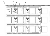
Fig. 6 is 5 * 5 matrix vertical views of similar electrochemical pixel device shown in Figure 1.
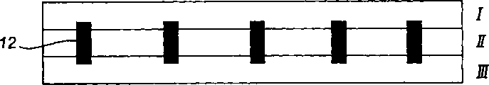
Fig. 7 illustrates 3 * 3 matrix vertical views of electrochemical pixel device according to another embodiment of the invention.
Fig. 8 A-8D illustrates according to another embodiment of the present invention, has another design of 3 * 3 matrixes of the electrochemical pixel device of vertical three layers of design.Fig. 8 A is the vertical view that has only bottom.Fig. 8 B is the vertical view that has only the middle level.Fig. 8 C is the vertical view that has only top layer.Fig. 8 D is the xsect of its side, three of Fig. 8 A-8C is shown is laminated together to form the electrochemical pixel device matrix.
The explanation of preferred embodiment
Definition:
Source contact: electrically contact (the electrical contact) of charge carrier to transistor channel is provided.
Drain contact: receive electrically contacting from transistorized charge carrier.
Gate electrode: any part and the solidified electrolyte of surf zone directly electrically contact, thus with electrically contacting that galvanochemistry active component ion contacts.
The galvanochemistry active component: " galvanochemistry active component " of the present invention is a kind of sheet material that comprises organic material, and the variation of the redox state that the conductivity of organic material can be by described organic material galvanochemistry takes place changes.The galvanochemistry active component contacts with at least one gate electrode ion by a kind of solidified electrolyte.This galvanochemistry active component can also and each source contact and drain contact or and both are combined into integral body these, this source contact and drain contact are made up of identical or different material.Galvanochemistry active component among the electrochemical transistor device A in electrochemical pixel device of the present invention comprises transistor channel.
Transistor channel: " transistor channel " of galvanochemistry active component set up electrically contacting between source contact and the drain contact.
Redox groove volume: in some embodiment of electrochemical transistor A, the galvanochemistry active component also comprises " redox groove volume ".This be near and and a part of galvanochemistry active component of directly electrically contacting of transistor channel, it provides or receives and flows to or from the electronics of transistor channel.Therefore, any redox reaction in transistor channel is replenished by the opposing reaction (opposing reactions) in this redox groove volume.
Redox state: when the variation of " redox state " of mentioning galvanochemistry active component and electric driven color-changing part, it is intended to comprise the situation that the material in this element not only oxidation takes place but also reduces, and electric charge situation about in this element, redistributing, make an end (end) be reduced and another end is oxidized.In the latter case, this element is whole to keep its total redox state, and according to definition used in this application, because the inside of charge carrier is redistributed, its redox state never changes.
Electric driven color-changing part: " electric driven color-changing part " in device of the present invention is a kind of continuous geometry body, and it can form different shapes, and it is made up of a kind of material or is made up of different materials.This material can be organic or inorganic, molecule or polymerization.This electric driven color-changing part, no matter its to be made up of a kind of material still be that combination of materials by more than one forms, it has the combination of following performance: at least a material conducts electricity under at least one oxidation state, with at least a material be electrochromic, promptly owing to the electrochemical redox reaction in this material presents change color.
Solidified electrolyte: for purposes of the invention, " solidified electrolyte " is a kind of enough hard under its serviceability temperature, the electrolyte that the particle/fragment in its body (bulk) is fixed by this electrolytical high viscosity/hardness basically and do not flowed or leak.In the preferred case, this electrolyte has suitable rheological properties and makes this material for example be coated on the supporting mass with traditional printing process with full wafer or a kind of mode easily.After the deposition, this electrolyte preparations can solidify when solvent evaporation, or because chemical reagent that adds or physical influence ultraviolet for example, infrared radiation or microwave radiation, cooling or any other method and chemical crosslink reaction takes place.Solidified electrolyte preferably includes moisture or contains the gel of organic solvent, for example gelatin or polymer latex.But also can consider the solid polymerization electrolyte, these electrolyte are also in protection scope of the present invention.And this definition also comprises liquid electrolyte solution, and this electrolyte solution immerses or for example paper, fabric or porous polymer support (hosted) by suitable host material with other any way.In some embodiments of the present invention, this material in fact is the supporting mass that is furnished with electrochemical pixel device on it, makes this supporting mass form the integrated operation part of this device.
Electrode: the structure that " electrode " in the device of the present invention is made up of conductive material.This electrode is used for applying impressed voltage on electrolyte, and the electrochemical reaction of needs takes place thereby the electric field in solidified electrolyte keeps sufficiently long one period.
Directly electrically contact: the direct physical between the two-phase (for example electrode and electrolyte) that can use by the interface exchange charge contacts (mutual interface).Charge exchange by the interface can comprise the electron transfer between conductive phase, the ion migration that ionic conduction is alternate, or the conversion between electronic current and gas current, the conversion of this electronic current and gas current is by for example electrode and electrolyte, electrolyte and electric driven color-changing part, or the electrochemical means at the interface between electrolyte and the galvanochemistry active component, or the capacitive current (capacitive currents) that takes place by the charging owing to this Helmholtz (Helmholtz) layer at the interface carries out.
Change color: when mentioning " change color ", this also means the variation that comprises optical density or reflection coefficient, therefore " change color " for example consider from blueness to red, blue to colourless, bottle green to light green color, grey to the variation of white or Dark grey to light gray etc.
Material
Preferably, the solidified electrolyte in one or two among electrochemical transistor device A and the electrochromic device B comprises cementing agent.Preferred this cementing agent has gelling performance.This cementing agent is preferably selected from gelatin, gelatine derivative, polyacrylic acid, polymethylacrylic acid, poly-(vinylpyrrolidone), polysaccharide, polyacrylamide, polyurethane, polypropyleneoxide, polyethylene oxide, poly-(styrene sulfonic acid) and poly-(vinyl alcohol) and its salt and multipolymer; And can randomly carry out crosslinked.This solidified electrolyte preferably also comprises ion salt, if the cementing agent that uses is a gelatin, preferably includes magnesium sulphate.This solidified electrolyte preferably also contains for example magnesium chloride of hygroscopic salt, to keep liquid water content wherein.
The organic material that is used among the electrochemical transistor device A of electrochemical pixel device of the present invention is preferably included in a kind of polymkeric substance that conducts electricity under at least one oxidation state, the also optional polyanionic polymer that comprises.It is also conceivable that the combination for example organic material and a few polymeric material of polymer blend that comprise more than one polymeric materials, wherein different layers is made up of identical polymkeric substance or different polymkeric substance.The conducting polymer that is used for electrochemical transistor device of the present invention is preferably selected from polythiophene, polypyrrole, polyaniline, polyisothianaphthene, polystyrene (polyphenylene vinylenes) and its multipolymer, for example be described in the polymkeric substance in the following document: people such as J C Gustafsson are at Solid State Ionics, 69,145-152 (1994); Handbook of Oligo-and Polythiophenes, Ch 10.8, Ed D Fichou, Wiley-VCH, Weinhem (1999); People such as P Schottland are at Macromolecules, and 33,7051-7061 (2000); Technology Map Conductive Polymers, SRI Consulting (1999); M Onoda is at Journal of the Electrochemical Society, 141,338-341 (1994); MChandrasekar is at Conducting Polymers, Fundamentals and Applications, aPractical Approach, Kluwer Academic Publishers, Boston (1999); With people such as A J Epstein at Macromol Chem, Macromol Symp, 51,217-234 (1991).In particularly preferred embodiments, organic material is 3, the polymkeric substance of 4-dialkoxythiophene or multipolymer, and wherein said two alkoxys can be represented the optional oxygen-alkylidene-oxo bridge that replaces identical or different or together.In the most preferred embodiment, this polymkeric substance is to be selected from 3 of following substances, 4-dialkoxythiophene polymkeric substance or multipolymer: poly-(3,4-methylene dioxy thiophene), poly-(3,4-methylene dioxy thiophene) derivant, poly-(3,4-ethylidene dioxy thiophene), poly-(3,4-ethylidene dioxy thiophene) derivant, poly-(3,4-propylidene dioxy thiophene), poly-(3,4-propylidene dioxy thiophene) derivant, poly-(3,4-butylidene dioxy thiophene), poly-(3,4-butylidene dioxy thiophene) derivant and multipolymer thereof.Polyanion (polyanion) compound is poly-(styrene sulfonate) preferably.
In preferred embodiments, be used for electric driven color-changing part among the electrochromic device B of electrochemical pixel device of the present invention and comprise a kind of electrochromic polymeric compounds that under at least one oxidation state, conducts electricity as electrochromic material, the also optional polyanionic compound that comprises.The electrochromic polymeric compounds that is used for the electric driven color-changing part of electrochromic device of the present invention is preferably selected from the electrochromism polythiophene, the electrochromism polypyrrole, the electrochromism polyaniline, the electrochromism polyisothianaphthene, electrochromism polystyrene and its multipolymer, for example by people such as J C Gustafsson at Solid State Ionics, 69,145-152 (1994); Handbook of Oligo-and Polythiophenes, Ch 10.8, Ed D Fichou, Wiley-VCH, Weinhem (1999); People such as P Schottland are at Macromolecules, and 33,7051-7061 (2000); Technology Map Conductive Polymers, SRI Consulting (1999); M Onoda is at Journal of the Electrochemical Society, 141,338-341 (1994); M Chandrasekar is at Conducting Polymers, Fundamentals and Applications, a Practical Approach, Kluwer Academic Publishers, Boston (1999); With people such as A J Epstein at MacromolChem, Macromol Symp, 51, those polymkeric substance of describing among the 217-234 (1991).In preferred embodiments, this electrochromic polymeric compounds is 3, the polymkeric substance of 4-dialkoxythiophene or multipolymer, and wherein said two alkoxys can be represented the optional oxygen-alkylidene-oxo bridge that replaces identical or different or together.In the most preferred embodiment, this electrochromic polymeric compounds is to be selected from following 3,4-dialkoxythiophene polymkeric substance or multipolymer: poly-(3,4-methylene dioxy thiophene), poly-(3,4-methylene dioxy thiophene) derivant, poly-(3,4-ethylidene dioxy thiophene), poly-(3,4-ethylidene dioxy thiophene) derivant, poly-(3,4-propylidene dioxy thiophene), poly-(3,4-propylidene dioxy thiophene) derivant, poly-(3,4-butylidene dioxy thiophene), poly-(3,4-butylidene dioxy thiophene) derivant and its multipolymer.Polyanionic polymer is poly-(styrene sulfonate) preferably.Those of ordinary skills are understandable to be, in another embodiment of the present invention, this electrochromic material comprises any non-polymer material, the combination of different non-polymer materials and the combination of polymeric material and non-polymer material, it has electric conductivity and electrochromic property under at least one oxidation state.It is also conceivable that the combination electric driven color-changing part of polymer blend or which floor electrochromic material for example that comprises more than one polymeric materials, wherein different layers is made up of identical materials or different materials, for example is made up of two kinds of different electrochromic polymeric compounds for every layer.
For example, can use the compound substance of conductive material and electrochromic material, for example conducting particles such as tin oxide, ITO or ATO particle and polymkeric substance or non-polymer electrochromic material such as polyaniline, polypyrrole, polythiophene, nickel oxide, tygon ferrocene (polyvinylferrocene), polyviologen, tungsten oxide, yttrium oxide, molybdena and Prussian blue (ferric ferrocyanide).As the indefiniteness example of the electric driven color-changing part that is used for device of the present invention, can mention: a slice had not only been conducted electricity but also electrochromic PEDOT-PSS; A slice has Fe
2+/ SCN
-PEDOT-PSS, PEDOT-PSS had not only conducted electricity but also electrochromism and Fe
2+/ SCN
-It is the electrochromism component (seeing below) of adding; By the sheet that the electroconductive ITO particle contiguous network in the insulating polymer matrix is formed, this sheet and electrochromism WO3 coating directly electrically contact; By the sheet that the electroconductive ITO particle contiguous network in the insulating polymer matrix is formed, this sheet contacts with electrochromism component in being dissolved in electrolyte.
Embodiments more of the present invention also comprise the electrochromic material that is used to realize having more than one color pixel devices.In the electric driven color-changing part of this electrochromic device B or solidified electrolyte, this further electrochromic material can also be set, for example also comprise the electrochromism redox system, as colourless on the one hand Fe
2+And SCN
-Redox couple, be red Fe on the other hand
3+(SCN
-) (H
2O)
5Complex.As the example of indefiniteness, these materials can be selected from for example DMPA-5 of different azophenlyene, 10-dihydro-5,10-dimethyl azophenlyene, DEPA-5,10-dihydro-5,10-diethyl azophenlyene and DOPA-5,10-dihydro-5,10-dioctyl azophenlyene, be selected from TMPD-N, N, N ', N '-tetramethylbenzene diamines, TMBZ-N, N, N ', N '-tetramethyl benzidine, the TTF-tetrathiafulvalene, phenanthroline-iron complex, erioglaucine A, diphenylamine, paraethoxychry-soidine (p-ethoxychrysoidine), methylene blue, different indigo and phenol safranine with and composition thereof.
As mentioned above, the electrochromic device B in the electrochemical pixel device of the present invention can comprise redox active material, and its reason is different from additional coloration.Any in this redox active material and other electrochromic material of above just having enumerated can be identical or different.Therefore, can use any suitable antioxidant or anti-reductive agent, for example: organic substance, as vitamin C, alcohol, polyvalent alcohol (as glycerine) or sugar, the alcohol, polyvalent alcohol or the sugar that exist with high pH value when appropriate, conjugated polymer, oligomer and single molecule; Dead matter, as comprise can be oxidized material (as: Fe
2+To Fe
3+, Sn
2+To Sn
4+) salt, metal cluster (as: Cu bunch or Fe bunch) or comprise the material (as: Fe that can be reduced
3+To Fe
2+, Sn
4+To Sn
2+) salt; Metallo-organic complex is as ferrocene, phthalocyanine dye, metalloporphyrin (metallo-prophyrines).
In electrochemical pixel device of the present invention, preferably, the organic material among the electrochemical transistor device A is that the electrochromic material among polymkeric substance and the electrochromic device B comprises electrochromic polymeric compounds.Under most preferred situation, the polymkeric substance among electrochromic polymeric compounds among the electrochromic device B and the electrochemical transistor device A is an identical materials.
In some embodiments of electrochemical pixel device of the present invention, supporting mass is preferably selected from polyethylene terephthalate; Polyethylene Naphthalate; Tygon; Polypropylene; Paper; Coated paper, as be coated with resin, tygon or polyacrylic paper; Laminated paper (paper laminates); Cardboard; Corrugated board; Glass and polycarbonate.Supporting mass is also preferably reflexive.
The embodiment of electrochemical pixel device
The typical electrochemical pixel device of the schematically illustrated the present invention of Fig. 1.Electrochemical pixel device 1 builds up by suitable material (as mentioned above) is formed pattern, and it comprises electrochemical transistor device (2-5,10-11) and electrochromic device (6-9).The electrochemical transistor device comprises source contact 2 and drain contact 3.Be distributed between source contact 2 and the drain contact 3 and what directly electrically contact with it is galvanochemistry active component 4, its conductance changes by the gate voltage that is applied on the main gate electrode 5.Galvanochemistry active component 4 and part main gate electrode 5 dielectric substrate that is cured covers.In this embodiment, source contact 2, drain contact 3 and galvanochemistry active component 4 form by a continuous sheet.Be separated with narrow gap between this sheet material and the gate electrode 5, therefore, directly do not electrically contact between galvanochemistry active component 4 and the gate electrode 5.
Electrochromic device comprises electric driven color-changing part 6 and two electrodes 7,8.Solidified electrolyte layer 9 covers the electric driven color-changing part 6 and first electrode 7.Directly do not electrically contact between first electrode 7 and the electric driven color-changing part 6, and directly electrically contact between the electric driven color-changing part 6 and second electrode 8.First electrode 7 of electrochromic device directly electrically contacts with the source contact 2 of electrochemical transistor device or coincides.
When electrochemical pixel device 1 performance function, be electric driven color-changing part 6 supply variable color electric currents (coloringcurrent) or decolouring electric current (decolouring current) by the voltage that between drain contact 3 and electrode 8, applies corresponding to drain electrode-source voltage Vds.Actual provision is subjected to the control of the conductance in the galvanochemistry active component 4 for the electric current of electric driven color-changing part 6.This conductance is subjected to the control of the gate voltage Vg at main gate electrode 5 places conversely.In certain embodiments, gate voltage Vg can be applied between main gate electrode (positive gate electrode) the 5 and second negative gate electrode (negative gate electrode) 11, and negative gate electrode 11 can directly electrically contact or directly not electrically contact with galvanochemistry active component 4.A kind of replacement scheme is that gate voltage is applied between main gate electrode 5 and source contact 2 or the drain contact 3.
In the experiment of the electrochemical pixel device that uses this embodiment of the present invention, produce this device with following method: the raw material of use is Orgacon
TMPaillon foil, this paillon foil can be purchased from Agfa, and it comprises conduction and electrochromic polymer P EDOT-PSS (being doped with poly-(3,4-ethylidene dioxy thiophene) of poly-(styrene sulfonate)).With the drawing instrument that is equipped with scalpel pattern is delineated in the PEDOT-PSS substrate.The electrolyte that uses is available from Apoteksbolaget, the Blagel of Sweden
TMBeing coated with gel with silk screen print method, is that the vinyl paillon foil that has pattern (vinyl foil) of 45 μ m is as template (template) with thickness.Also can be used in the hydroxyethyl cellulose of 10% in the water as electrolyte gel.
PEDOT-PSS be under its natural partial oxidation attitude, have very light light blue and have a material of satisfactory electrical conductivity.When PEDOT-PSS reduced, its electric conductivity reduced greatly, and this material becomes mazarine.As in the described device with structure shown in Figure 1 just now, electrochromic device B is generally by the V of 1.5-2V at this PEDOT-PSS pixel device
DsDriven, display area is at 1-2cm
2Between change.After being reduced, electric driven color-changing part 6 in this case becomes mazarine.Also have oxidized electrode 7, otherwise electric driven color-changing part may be destroyed by peroxidating.This counter electrode is always not useful, because it has reduced effective display area, addresses this problem (vide infra to the explanation of Fig. 8 A-8D) but designed a kind of method with vertical stratification replacement side direction structure shown in Figure 1.
In the experiment of using the PEDOT-PSS pixel, the electric current by electrochromic device during beginning is about 200-300 μ A, V
DsBe 2V, the area of electric driven color-changing part is 1-2cm
2After about 10 seconds, this device is fully changed with saturated.The electric current that flows through electrochromic device under this state of saturation is about 50 μ A.Even also having the reason of this current value under the reduction of PEDOT-PSS, non-conductive state is the leakage of display device.
In these experiments, the electrochemical transistor device is driven by the gate voltage of 0-1.5V.When gate voltage was 0V, the galvanochemistry active component fully conducted electricity, and when 1.5V, was in "off" state.When 0.3-0.4V, can obviously find out from blue outward appearance: transistor channel is reduced, and this increases corresponding to resistance.Resistance in the transistor channel is about 10k Ω under its conduction state, the electric current of these 200 μ A during corresponding to 2V.Under dissengaged positions, when the gate voltage of about 1.5V, resistance increases greatly.Current value reaches about 200nA, corresponding to the resistance of 10M Ω.Therefore, in this case, the ON/OFF ratio of the electrochemical transistor device portions of electrochemical pixel device is 1000.In addition, when using the parts made from alternative method, the extreme ON/OFF ratio that reaches is 105.
The a few thing performance of this electrochemical pixel device is as follows:
-transistor channel conducts electricity when the gate voltage Vg of 0V, and is non-conductive basically when the gate voltage Vg of 1V.
If-reduce, promptly during mazarine, electric driven color-changing part is at V
DsDecolour when being 0V, otherwise can not take place whatever.At V
DsWhen being 2V, electrochemical reaction takes place, electric driven color-changing part becomes the mazarine state of its reduction, as long as be applied with voltage, just can remain on this state.
Be applied to the effect of four kinds of possible voltage combinations on the pixel:
Vg=0V, V
Ds=0V; Do not take place whatever, perhaps, if on beginning, be reduced, then pixel decolouring.
Vg=0V, V
Ds=2V; The pixel variable color keeps this state then.
Vg=1V, V
Ds=0V; Transistor channel becomes non-conductive.If pixel is reduced, then the impedance that increases in the raceway groove remains in the pixel region electric charge.
Vg=1V, V
Ds=2V; Do not take place whatever.
Fig. 2-the 4th is at the coordinate figure with the test result of carrying out on the PEDOT-PSS pixel device of design shown in Figure 1.Fig. 2 illustrates the V with 2V
DsMake the process of electrochromic device variable color.Transistor channel is in "open" state, i.e. Vg=0V.Electric current by raceway groove during beginning is about 150 μ A, descends owing to the electric driven color-changing part in the display device is reduced to non-conductive state then.In this test, the electric driven color-changing part area is 64mm
2, the counter electrode area is 90mm
2After about 5 seconds, pixel is changed fully.
Fig. 3 is the coordinate figure that is illustrated in pixel decolouring under two kinds of different situations.Above curve A be 1.4V corresponding to Vg, when promptly transistor channel is closed from the electric current of electric driven color-changing part.Below curve B Vg is shown is 0V, when promptly transistor channel is open from the electric current of electric driven color-changing part.
Fig. 4 is the coordinate figure of a pixel decolouring when being illustrated in different Vg value.Closing (Vg=1.4V) at 50 seconds transistor channels, was open (Vg=0V) at back 10 seconds.Can clearly be seen that from Fig. 4: electric driven color-changing part, still have a large amount of electric charges after 50 seconds in decolouring under the situation that transistor channel is closed.Open when transistor channel, when promptly gate voltage was set to 0V, the decolouring current peak appearred.The size at this peak is about 20 μ A, and the leakage current of hundreds of nA was compared when this can close with raceway groove.
The side direction matrix of electrochemical pixel device
Use identical materials in the electrochemical pixel device with embodiment described in the last branch to realize several different matrix of electrochemical pixel device.
Shown in Figure 5 is 5 pixels of row or 5 * 1 matrixes.Use the label among Fig. 1, the drain contact 3 of each pixel in 5 pixels all with is simultaneously supplied V for all pixels
DsConductor connect.On the contrary, gate electrode 5 and 11 layout are that each gate voltage is applied on each pixel independently.
Fig. 6 illustrates more complicated, the also more useful matrix of electrochemical pixel device.Here, 5 row, 5 pixels in 5 * 5 matrixes, have been made up.With the contact of row and column can be that row apply variable color or decolouring V simultaneously
Ds, and transistorized gate electrode links together, thus all crystals pipe that can be independent of in the delegation of other row transistor is set to " opening " or " pass ".
For simplified design, for the conductor that is reduced to each electrode supply of current and the crossing number between the contact, form 3 * 3 matrixes with a variant of electrochemical pixel device, this matrix is as shown in Figure 7.In this variant, do not use negative gate electrode 11, this means conductor of few use.In addition, in the matrix of the device that uses two gate electrodes, the problem of cross-talk may appear producing between pixel by the conductor that connects negative gate electrode.It is a kind of method that addresses this problem that each pixel device only uses a gate electrode.Another kind of substituting method is that a resistance (this with vertical matrix design below in illustrate) is set on each negative electrode 11.
The vertical matrix of electrochemical pixel device
With reference now to Fig. 8 A-8D,, 3 * 3 matrixes of the same electrochemical pixel device of vertical design shown in the figure.This matrix is formed by three different layers, and these layer interlayer structures form electrochemical pixel device group (ensemble) together.Bottom I shown in Fig. 8 A comprises the galvanochemistry active component 4 of each transistor device.Also have main gate electrode (5) and negative gate electrode (11) to reach the conductor that is connected with each row gate electrode in this layer.In order to reduce cross-talk, all be provided with resistance on the negative gate electrode 11, resistance is expressed as the line segment that interrupts each negative gate electrode 11 in the drawings.Also have the source contact 2 of electrochemical transistor device and an electrode 7 of drain contact 3 and electrochromic device in this layer.
Fig. 8 B illustrates middle layer II or wall.This layer is included in the necessary solidified electrolyte element of electrochemical reaction takes place in the electrochemical pixel device.Therefore the electrolyte 9 that is used for electrochromic device B is provided, has made that electrolyte 9 contacts with the electrode 7 of bottom I and the electric driven color-changing part 6 of top layer III when these layers combine.The electrolyte 10 that is used for electrochemical transistor device A is provided equally, has made that electrolyte 10 contacts with gate electrode 5 with the galvanochemistry active component 4 of bottom when these layers combine.Middle layer II also comprises passage (vias) 12, and passage 12 is formed by conductive material, is used to mediate drain contact 3 delivered charge to bottom I from following top layer III.
Fig. 8 C illustrates top layer III.In this layer, conductor 13 is top layer supply V by the passage 12 in middle layer
Ds, bottom also comprises the electric driven color-changing part 6 of vertical electrochromic device.In this special embodiment, the electric driven color-changing part 6 of all pixels is to be formed by the material with a slice electrochromism and conduction in the row, is the electrochemical pixel device supply V in these row
DsElectrode 8 can be considered in this sheet not those parts of contacting with following gel electrolyte.This layout can be drain contact 3 and electrode 8 supply V with the mode of operation that is similar to single side direction electrochemical pixel device shown in Figure 1
DsTop layer III also comprises zone 14, and this zone 14 is non-conductive or isolated, and contacts with electrochemical transistor device electrolyte 10 in the above-mentioned layer, is used for preventing from galvanochemistry active component 4 leakage currents.
Fig. 8 D is the sketch of three layers when combining, and the fundamental purpose of this figure is a demonstration passage 12, has set up between the parts of passage 12 for layer I and III to electrically contact.
Claims (39)
1, a kind of pixel device, it comprises following parts:
(A) electrochemical transistor device, it comprises: source contact; Drain contact; At least one gate electrode; The galvanochemistry active component that is arranged between source contact and the drain contact and directly electrically contacts with it, the galvanochemistry active component comprises transistor channel, and is that a kind of comprising can be by changing the material that its redox state electrochemically changes the organic material of its conductivity; And galvanochemistry active component and described at least one gate electrode directly electrically contact and insert solidified electrolyte between the two, flow to prevent the electronics between galvanochemistry active component and the described gate electrode; Thus, utilize the voltage that applies on the described gate electrode can the Controlling Source polar contact and drain contact between electronics flow and
(B) electrochromic device, it comprises: at least one electric driven color-changing part, this element comprises (i) at least a material that can conduct electricity and (ii) at least a electrochromic material under at least a oxidation state, wherein, and described material (i) and (ii) can be identical or different; At least the solidified electrolyte layer that directly electrically contacts of one deck and described electric driven color-changing part; At least two are applicable to the electrode that applies voltage betwixt; Each described electrode all directly electrically contacts with the parts that are selected from described dielectric substrate and described electric driven color-changing part;
In this pixel device, in the described source contact of electrochemical transistor device A and the drain contact one with electrochromic device B in an electrode electrically contact.
2, according to the electrochemical pixel device of claim 1, wherein, an electrode among the source contact of electrochemical transistor device A and the electrochromic device B electrically contacts.
3, according to the electrochemical pixel device of claim 1, wherein, an electrode among the drain contact of electrochemical transistor device A and the electrochromic device B electrically contacts.
4, according to the electrochemical pixel device of claim 1, wherein, the described source contact of electrochemical transistor device A and drain contact, gate electrode and galvanochemistry active component all are arranged on the common plane.
5, according to the electrochemical pixel device of claim 4, wherein, in electrochemical transistor device A, continuous or interrupted solidified electrolyte layer covers the galvanochemistry active component and covers described gate electrode to small part.
6, according to the electrochemical pixel device of claim 1, wherein, in electrochemical transistor device A, at least one in described source contact and drain contact and the gate electrode used with galvanochemistry active component identical materials and made.
7, according to the electrochemical pixel device of claim 6, wherein, in electrochemical transistor device A, described source contact and drain contact and gate electrode are all used with galvanochemistry active component identical materials and are made.
8, according to the electrochemical pixel device of claim 7, wherein, in electrochemical transistor device A, source contact and drain contact and galvanochemistry active component form by a serialgram that comprises the described material of organic material.
9, according to the electrochemical pixel device of claim 1, wherein, in electrochromic device B, electrode is used with the electric driven color-changing part identical materials and is made.
10, according to the electrochemical pixel device of claim 1, wherein, electric driven color-changing part and the electrode of the source contact of electrochemical transistor device A and drain contact, galvanochemistry active component and gate electrode and electrochromic device B are all made with identical materials.
11, according to the electrochemical pixel device of claim 1, wherein, in electrochemical transistor device A, organic material is a polymkeric substance.
12, according to the electrochemical pixel device of claim 11, wherein, in electrochromic device B, electrochromic material is an electrochromic polymeric compounds.
13, according to the electrochemical pixel device of claim 12, wherein, the polymkeric substance among electrochromic polymeric compounds among the electrochromic device B and the electrochemical transistor device A is a same material.
14, according to each electrochemical pixel device among the claim 11-13, wherein, all polymkeric substance that exist among all electrochromic polymeric compounds that exist among the electrochromic device B and the electrochemical transistor device A all are selected from polythiophene, polypyrrole, polyaniline, polyisothianaphthene, polystyrene and its multipolymer.
15, according to the electrochemical pixel device of claim 14, wherein, all polymkeric substance that exist among all electrochromic polymeric compounds that exist among the electrochromic device B and the electrochemical transistor device A all are 3, the polymkeric substance of 4-dialkoxythiophene or multipolymer, two alkoxys wherein can be represented the optional oxygen-alkylidene-oxo bridge that replaces identical or different or together.
16, according to the electrochemical pixel device of claim 15, wherein, described 3, the polymkeric substance of 4-dialkoxythiophene or multipolymer are selected from poly-(3,4-methylene dioxy thiophene), poly-(3,4-methylene dioxy thiophene) derivant, poly-(3,4-ethylidene dioxy thiophene), poly-(3,4-ethylidene dioxy thiophene) derivant, poly-(3,4-propylidene dioxy thiophene), poly-(3,4-propylidene dioxy thiophene) derivant, poly-(3,4-butylidene dioxy thiophene), poly-(3,4-butylidene dioxy thiophene) derivant and multipolymer thereof.
17, according to the electrochemical pixel device of claim 1, wherein, the organic material among electrochromic material among the electrochromic device B and/or the electrochemical transistor device A comprises polyanionic compound.
18, according to the electrochemical pixel device of claim 17, wherein, described polyanionic compound is poly-(styrene sulfonate) or its salt.
19, according to the electrochemical pixel device of claim 1, wherein, solidified electrolyte among the electrochemical transistor device A and/or the solidified electrolyte among the electrochromic device B comprise cementing agent.
20, according to the electrochemical pixel device of claim 19, wherein, described cementing agent is a jelling agent, be selected from gelatin, gelatine derivative, polyacrylic acid, polymethylacrylic acid, poly-(vinylpyrrolidone), polysaccharide, polyacrylamide, polyurethane, polypropyleneoxide, polyethylene oxide, poly-(styrene sulfonic acid) and poly-(vinyl alcohol) and its salt and multipolymer.
21, according to the electrochemical pixel device of claim 1, wherein, solidified electrolyte among the electrochemical transistor device A and/or the solidified electrolyte among the electrochromic device B comprise ion salt.
22, according to the electrochemical pixel device of claim 1, wherein, same solidified electrolyte not only is used among the electrochemical transistor device A but also is used among the electrochromic device B.
23, according to the electrochemical pixel device of claim 1, it is arranged on the supporting mass.
24, according to the electrochemical pixel device of claim 23, wherein, described supporting mass is selected from paper, laminated paper, cardboard, corrugated board and the glass of polyethylene terephthalate, Polyethylene Naphthalate, tygon, polypropylene, polycarbonate, paper, coated paper, resin-coating.
25, according to the electrochemical pixel device of claim 23 or 24, wherein, described supporting mass is reflexive.
26, according to the electrochemical pixel device of claim 1, wherein, in electrochromic device B, electrode and electric driven color-changing part are arranged side by side in common plane.
27, according to the electrochemical pixel device of claim 1, wherein, in electrochromic device B, electrode and electric driven color-changing part are arranged vertically.
28, a kind of matrix comprises a plurality of according to each electrochemical pixel device among the claim 1-27.
29, according to the matrix of claim 28, wherein, each electrochemical pixel device has a gate electrode.
30, according to the matrix of claim 28, wherein, each electrochemical pixel device has at least two gate electrodes, and a gate electrode of each electrochemical pixel device is provided with a resistance, to reduce the cross-talk between the pixel.
31, a kind of pixellated display, it comprises according to each matrix among the claim 28-30.
32, a kind of method of producing according to the electrochemical pixel device of claim 1, this method are included in the described contact of deposition, electrode, galvanochemistry active component, electric driven color-changing part and electrolyte on the supporting mass.
33, according to the method for claim 32, wherein, deposit described contact, electrode, galvanochemistry active component, electric driven color-changing part and/or electrolyte with printing technology.
34, according to the method for claim 32, wherein, deposit described contact, electrode, galvanochemistry active component, electric driven color-changing part and electrolyte with coating technique.
35, according to each method among the claim 32-34, in device, the described organic material of electrochemical transistor device A and/or the described electric driven color-changing part of electrochromic device B comprise polymkeric substance, this method comprise by on-site polymerization with described polymer deposition on supporting mass.
36, according to the method for claim 32, it comprises with any formation pattern in subtraction docking point, electrode, galvanochemistry active component and the electric driven color-changing part.
37, according to the method for claim 36, wherein, described formation pattern is undertaken by chemical etching.
38, according to the method for claim 36, wherein, described formation pattern is undertaken by cavitation erosion.
39, according to the method for claim 36, wherein, described formation pattern is undertaken by mechanical means, and mechanical means comprises friction, hacks quarter, swipes and mills.
Applications Claiming Priority (8)
| Application Number | Priority Date | Filing Date | Title |
|---|---|---|---|
| SE0100748A SE520339C2 (en) | 2001-03-07 | 2001-03-07 | Electrochemical transistor device, used for e.g. polymer batteries, includes active element having transistor channel made of organic material and gate electrode where voltage is applied to control electron flow |
| SE0100747A SE521552C2 (en) | 2001-03-07 | 2001-03-07 | Electrochromic device for providing display, has electrochromic element comprising electrically-conducting electrochromic materials |
| SE01007483 | 2001-03-07 | ||
| SE01007475 | 2001-03-07 | ||
| US27621801P | 2001-03-16 | 2001-03-16 | |
| US27610501P | 2001-03-16 | 2001-03-16 | |
| US60/276,218 | 2001-03-16 | ||
| US60/276,105 | 2001-03-16 |
Publications (2)
| Publication Number | Publication Date |
|---|---|
| CN1496491A CN1496491A (en) | 2004-05-12 |
| CN1224862C true CN1224862C (en) | 2005-10-26 |
Family
ID=29718695
Family Applications (1)
| Application Number | Title | Priority Date | Filing Date |
|---|---|---|---|
| CNB028061276A Expired - Fee Related CN1224862C (en) | 2001-03-07 | 2002-03-07 | Electrochemical pixel device |
Country Status (7)
| Country | Link |
|---|---|
| US (1) | US6642069B2 (en) |
| EP (1) | EP1373976B1 (en) |
| JP (1) | JP4256163B2 (en) |
| CN (1) | CN1224862C (en) |
| AT (1) | ATE393411T1 (en) |
| DE (1) | DE60226221T2 (en) |
| WO (1) | WO2002071139A1 (en) |
Families Citing this family (51)
| Publication number | Priority date | Publication date | Assignee | Title |
|---|---|---|---|---|
| US7034791B1 (en) | 2000-12-14 | 2006-04-25 | Gary Odom | Digital video display employing minimal visual conveyance |
| US7012306B2 (en) * | 2001-03-07 | 2006-03-14 | Acreo Ab | Electrochemical device |
| US6756620B2 (en) * | 2001-06-29 | 2004-06-29 | Intel Corporation | Low-voltage and interface damage-free polymer memory device |
| US6624457B2 (en) | 2001-07-20 | 2003-09-23 | Intel Corporation | Stepped structure for a multi-rank, stacked polymer memory device and method of making same |
| EP1487935A1 (en) * | 2002-03-07 | 2004-12-22 | Acreo AB | Electrochemical device |
| DE10300521A1 (en) * | 2003-01-09 | 2004-07-22 | Siemens Ag | Organoresistive memory |
| DE10324388A1 (en) * | 2003-05-28 | 2004-12-30 | Infineon Technologies Ag | Circuit element with a first layer of an electrically insulating substrate material and method for producing a circuit element |
| ES2223289B1 (en) * | 2003-08-05 | 2006-04-16 | Fundacion Cidetec | ELECTROCHROME DEVICE BASED ON DRIVING POLYMERS, THE PROCEDURE FOR OBTAINING THE SAME, AS WELL AS THE PRODUCT OBTAINED. |
| US7163734B2 (en) * | 2003-08-26 | 2007-01-16 | Eastman Kodak Company | Patterning of electrically conductive layers by ink printing methods |
| SE526873C2 (en) * | 2003-12-02 | 2005-11-15 | Acreo Ab | Wettability switch comprising an electrochemically active element with interchangeable surface wetting properties, process for its manufacture and its use in various applications |
| US20060138944A1 (en) * | 2004-12-27 | 2006-06-29 | Quantum Paper | Addressable and printable emissive display |
| EP1836879A2 (en) * | 2004-12-27 | 2007-09-26 | Quantum Paper, Inc. | Addressable and printable emissive display |
| US20060138948A1 (en) * | 2004-12-27 | 2006-06-29 | Quantum Paper, Inc. | Addressable and printable emissive display |
| JP2006286664A (en) * | 2005-03-31 | 2006-10-19 | Toshiba Corp | Organic electroluminescent element |
| US7443566B2 (en) * | 2006-03-10 | 2008-10-28 | Sony Ericsson Mobile Communications Ab | Low power, configurable display for mobile devices |
| EP1921496A1 (en) * | 2006-11-08 | 2008-05-14 | Acreo AB | Electrochromic device |
| GB0623108D0 (en) * | 2006-11-20 | 2006-12-27 | Sericol Ltd | A printable composition |
| EP1988514A1 (en) * | 2007-05-04 | 2008-11-05 | Acreo AB | Security document circuit |
| US8877101B2 (en) | 2007-05-31 | 2014-11-04 | Nthdegree Technologies Worldwide Inc | Method of manufacturing a light emitting, power generating or other electronic apparatus |
| US9425357B2 (en) | 2007-05-31 | 2016-08-23 | Nthdegree Technologies Worldwide Inc. | Diode for a printable composition |
| US9343593B2 (en) | 2007-05-31 | 2016-05-17 | Nthdegree Technologies Worldwide Inc | Printable composition of a liquid or gel suspension of diodes |
| US9018833B2 (en) | 2007-05-31 | 2015-04-28 | Nthdegree Technologies Worldwide Inc | Apparatus with light emitting or absorbing diodes |
| US9534772B2 (en) | 2007-05-31 | 2017-01-03 | Nthdegree Technologies Worldwide Inc | Apparatus with light emitting diodes |
| US9419179B2 (en) | 2007-05-31 | 2016-08-16 | Nthdegree Technologies Worldwide Inc | Diode for a printable composition |
| US8674593B2 (en) | 2007-05-31 | 2014-03-18 | Nthdegree Technologies Worldwide Inc | Diode for a printable composition |
| US8889216B2 (en) * | 2007-05-31 | 2014-11-18 | Nthdegree Technologies Worldwide Inc | Method of manufacturing addressable and static electronic displays |
| US8852467B2 (en) | 2007-05-31 | 2014-10-07 | Nthdegree Technologies Worldwide Inc | Method of manufacturing a printable composition of a liquid or gel suspension of diodes |
| US8456393B2 (en) | 2007-05-31 | 2013-06-04 | Nthdegree Technologies Worldwide Inc | Method of manufacturing a light emitting, photovoltaic or other electronic apparatus and system |
| US8415879B2 (en) | 2007-05-31 | 2013-04-09 | Nthdegree Technologies Worldwide Inc | Diode for a printable composition |
| US8846457B2 (en) | 2007-05-31 | 2014-09-30 | Nthdegree Technologies Worldwide Inc | Printable composition of a liquid or gel suspension of diodes |
| US8809126B2 (en) | 2007-05-31 | 2014-08-19 | Nthdegree Technologies Worldwide Inc | Printable composition of a liquid or gel suspension of diodes |
| GB2449928A (en) * | 2007-06-08 | 2008-12-10 | Seiko Epson Corp | Electrochemical thin-film transistor |
| GB2454203A (en) * | 2007-10-30 | 2009-05-06 | Univ Muenster Wilhelms | Time controlled activation of elements |
| US7724499B2 (en) | 2007-11-13 | 2010-05-25 | Industrial Technology Research Institute | Electrolyte transistor |
| US7992332B2 (en) * | 2008-05-13 | 2011-08-09 | Nthdegree Technologies Worldwide Inc. | Apparatuses for providing power for illumination of a display object |
| US8127477B2 (en) | 2008-05-13 | 2012-03-06 | Nthdegree Technologies Worldwide Inc | Illuminating display systems |
| FI20085737L (en) * | 2008-07-21 | 2010-01-22 | Ronald Oesterbacka | Components and circuit arrangements with at least one organic field effect transistor |
| WO2010028329A1 (en) * | 2008-09-08 | 2010-03-11 | Ntera Inc | Printed display systems based on porous substrates |
| WO2010114793A2 (en) * | 2009-04-03 | 2010-10-07 | Ciba Corporation | Devices containing compositions comprising cathodically coloring electrochromic polymers and binder polymers |
| JP5694334B2 (en) | 2009-10-05 | 2015-04-01 | アクレオ スウェディッシュ イーセーティー アーベー | Electrochemical devices |
| SE534488C2 (en) | 2010-02-22 | 2011-09-06 | Lunavation Ab | A system for electrokinetic flow technology |
| EP2554365A4 (en) * | 2010-03-26 | 2017-08-09 | Tohoku University | Porous structure provided with pattern that is composed of conductive polymer, and method for producing same |
| DE102010026098A1 (en) * | 2010-07-05 | 2012-01-05 | Forschungszentrum Jülich GmbH | Ionically controlled three-electrode component |
| US9709867B2 (en) | 2010-10-05 | 2017-07-18 | Rise Acreo Ab | Display device |
| TW201215980A (en) * | 2010-10-05 | 2012-04-16 | J Touch Corp | Electrochromic module and stereoscopic image display device having the same |
| JP6035458B2 (en) | 2011-04-05 | 2016-12-07 | リンテック株式会社 | Method for manufacturing electrochemical devices based on self-aligned electrolyte on electrodes |
| WO2013161633A1 (en) | 2012-04-23 | 2013-10-31 | 株式会社村田製作所 | Conductive composition, composite material and production method therefor |
| JP6054763B2 (en) * | 2013-02-12 | 2016-12-27 | 株式会社ジャパンディスプレイ | Organic EL display device |
| US10312731B2 (en) | 2014-04-24 | 2019-06-04 | Westrock Shared Services, Llc | Powered shelf system for inductively powering electrical components of consumer product packages |
| WO2019039121A1 (en) * | 2017-08-23 | 2019-02-28 | 国立研究開発法人物質・材料研究機構 | Electrochromic element and display system using same |
| US10135015B1 (en) * | 2017-11-02 | 2018-11-20 | Palo Alto Research Center Incorporated | Electrochemical clock and oscillator devices |
Family Cites Families (22)
| Publication number | Priority date | Publication date | Assignee | Title |
|---|---|---|---|---|
| US4764415A (en) | 1986-07-01 | 1988-08-16 | Mitsubishi Denki Kabushiki Kaisha | Electric element using oxidation-reduction substances |
| US4993810A (en) | 1989-04-14 | 1991-02-19 | Ford Motor Company | Electrochromic devices comprising metal salts in an ion conductive material |
| US5049868A (en) * | 1989-09-19 | 1991-09-17 | Rockwell International Corporation | Electrochromic display dot drive matrix |
| IT1237269B (en) * | 1989-11-15 | 1993-05-27 | NEURAL NETWORK WITH LEARNING SKILLS FOR THE PROCESSING OF INFORMATION, AND PROCEDURE FOR THE TREATMENT OF INFORMATION WITH THE USE OF SUCH NETWORK. | |
| EP0440957B1 (en) | 1990-02-08 | 1996-03-27 | Bayer Ag | New polythiophene dispersions, their preparation and their use |
| US5189549A (en) | 1990-02-26 | 1993-02-23 | Molecular Displays, Inc. | Electrochromic, electroluminescent and electrochemiluminescent displays |
| FR2664430B1 (en) | 1990-07-04 | 1992-09-18 | Centre Nat Rech Scient | THIN FILM FIELD EFFECT TRANSISTOR WITH MIS STRUCTURE, IN WHICH THE INSULATION AND THE SEMICONDUCTOR ARE MADE OF ORGANIC MATERIALS. |
| US5138481A (en) | 1991-07-23 | 1992-08-11 | Ford Motor Company | Electrochromic device with color gradient and method of making the device |
| US5413739A (en) | 1992-12-22 | 1995-05-09 | Coleman; James P. | Electrochromic materials and displays |
| US5754329A (en) | 1992-12-22 | 1998-05-19 | Monsanto Company | Electrochromic display laminates |
| WO1994016356A1 (en) * | 1993-01-05 | 1994-07-21 | Martin Marietta Corporation | Improved electrode for display devices |
| FR2746934B1 (en) * | 1996-03-27 | 1998-05-07 | Saint Gobain Vitrage | ELECTROCHEMICAL DEVICE |
| US6369934B1 (en) * | 1996-05-30 | 2002-04-09 | Midwest Research Institute | Self bleaching photoelectrochemical-electrochromic device |
| DE19622600C2 (en) * | 1996-06-05 | 2001-08-02 | Fraunhofer Ges Forschung | Electrochromic unit |
| GB2324883A (en) * | 1997-04-28 | 1998-11-04 | Wisconsin Label Corp | Self-powered electrochemical display cell with focused field |
| US5877888A (en) | 1997-06-10 | 1999-03-02 | Monsanto Company | Single and double sided electrochromic displays |
| WO1999010939A2 (en) | 1997-08-22 | 1999-03-04 | Koninklijke Philips Electronics N.V. | A method of manufacturing a field-effect transistor substantially consisting of organic materials |
| DE19810932A1 (en) | 1998-03-13 | 1999-09-16 | Bayer Ag | Electrochromic arrangement based on poly (3,4-ethylenedioxy-thiophene) derivatives |
| US6118572A (en) | 1998-07-01 | 2000-09-12 | The Regents Of The University Of California | Photochromic, electrochromic, photoelectrochromic and photovoltaic devices |
| US6506438B2 (en) | 1998-12-15 | 2003-01-14 | E Ink Corporation | Method for printing of transistor arrays on plastic substrates |
| US6387727B1 (en) | 1999-03-29 | 2002-05-14 | Agere Systems Guardian Corp. | Device comprising n-channel semiconductor material |
| US6444400B1 (en) | 1999-08-23 | 2002-09-03 | Agfa-Gevaert | Method of making an electroconductive pattern on a support |
-
2002
- 2002-03-07 AT AT02704001T patent/ATE393411T1/en not_active IP Right Cessation
- 2002-03-07 US US10/091,397 patent/US6642069B2/en not_active Expired - Lifetime
- 2002-03-07 EP EP02704001A patent/EP1373976B1/en not_active Expired - Lifetime
- 2002-03-07 CN CNB028061276A patent/CN1224862C/en not_active Expired - Fee Related
- 2002-03-07 JP JP2002569996A patent/JP4256163B2/en not_active Expired - Fee Related
- 2002-03-07 DE DE60226221T patent/DE60226221T2/en not_active Expired - Lifetime
- 2002-03-07 WO PCT/SE2002/000404 patent/WO2002071139A1/en active Application Filing
Also Published As
| Publication number | Publication date |
|---|---|
| JP4256163B2 (en) | 2009-04-22 |
| JP2004522189A (en) | 2004-07-22 |
| US20020134980A1 (en) | 2002-09-26 |
| EP1373976A1 (en) | 2004-01-02 |
| CN1496491A (en) | 2004-05-12 |
| DE60226221D1 (en) | 2008-06-05 |
| US6642069B2 (en) | 2003-11-04 |
| WO2002071139A1 (en) | 2002-09-12 |
| ATE393411T1 (en) | 2008-05-15 |
| EP1373976B1 (en) | 2008-04-23 |
| DE60226221T2 (en) | 2009-05-14 |
Similar Documents
| Publication | Publication Date | Title |
|---|---|---|
| CN1224862C (en) | Electrochemical pixel device | |
| CN1222819C (en) | Electrochromic device | |
| US9829764B2 (en) | Multi-color electrophoretic displays | |
| US7301687B2 (en) | Electrochemical device | |
| US8089453B2 (en) | Stylus-based addressing structures for displays | |
| US7956841B2 (en) | Stylus-based addressing structures for displays | |
| US7352353B2 (en) | Electrostatically addressable electrophoretic display | |
| US6535197B1 (en) | Printable electrode structures for displays | |
| KR101329628B1 (en) | Circuit board and manufacturing method thereof, electro-optical device, and electronic apparatus | |
| US6842167B2 (en) | Rear electrode structures for displays | |
| US20040090415A1 (en) | Rear electrode structures for electrophoretic displays | |
| CN102414610A (en) | Electrochromic display apparatus | |
| EP1208603A1 (en) | Transistor for an electronically driven display | |
| CN1304897C (en) | Electrochemical device | |
| EP1507165A1 (en) | Novel addressing schemes for electrophoretic displays | |
| Berggren et al. | 7 Electrochromic Displays |
Legal Events
| Date | Code | Title | Description |
|---|---|---|---|
| C06 | Publication | ||
| PB01 | Publication | ||
| C10 | Entry into substantive examination | ||
| SE01 | Entry into force of request for substantive examination | ||
| C14 | Grant of patent or utility model | ||
| GR01 | Patent grant | ||
| CF01 | Termination of patent right due to non-payment of annual fee | ||
| CF01 | Termination of patent right due to non-payment of annual fee |
Granted publication date: 20051026 Termination date: 20190307 |