CN1157943C - Selective gain adjustement to aid carrier acquisition in a high definition television receiver - Google Patents
Selective gain adjustement to aid carrier acquisition in a high definition television receiver Download PDFInfo
- Publication number
- CN1157943C CN1157943C CNB008104735A CN00810473A CN1157943C CN 1157943 C CN1157943 C CN 1157943C CN B008104735 A CNB008104735 A CN B008104735A CN 00810473 A CN00810473 A CN 00810473A CN 1157943 C CN1157943 C CN 1157943C
- Authority
- CN
- China
- Prior art keywords
- signal
- amplification
- control signal
- amplification level
- pilot tone
- Prior art date
- Legal status (The legal status is an assumption and is not a legal conclusion. Google has not performed a legal analysis and makes no representation as to the accuracy of the status listed.)
- Expired - Fee Related
Links
Images


Classifications
-
- H—ELECTRICITY
- H04—ELECTRIC COMMUNICATION TECHNIQUE
- H04N—PICTORIAL COMMUNICATION, e.g. TELEVISION
- H04N5/00—Details of television systems
- H04N5/44—Receiver circuitry for the reception of television signals according to analogue transmission standards
- H04N5/455—Demodulation-circuits
-
- H—ELECTRICITY
- H04—ELECTRIC COMMUNICATION TECHNIQUE
- H04N—PICTORIAL COMMUNICATION, e.g. TELEVISION
- H04N7/00—Television systems
- H04N7/015—High-definition television systems
-
- H—ELECTRICITY
- H04—ELECTRIC COMMUNICATION TECHNIQUE
- H04N—PICTORIAL COMMUNICATION, e.g. TELEVISION
- H04N21/00—Selective content distribution, e.g. interactive television or video on demand [VOD]
- H04N21/40—Client devices specifically adapted for the reception of or interaction with content, e.g. set-top-box [STB]; Operations thereof
- H04N21/41—Structure of client; Structure of client peripherals
- H04N21/426—Internal components of the client ; Characteristics thereof
- H04N21/42607—Internal components of the client ; Characteristics thereof for processing the incoming bitstream
-
- H—ELECTRICITY
- H04—ELECTRIC COMMUNICATION TECHNIQUE
- H04N—PICTORIAL COMMUNICATION, e.g. TELEVISION
- H04N21/00—Selective content distribution, e.g. interactive television or video on demand [VOD]
- H04N21/40—Client devices specifically adapted for the reception of or interaction with content, e.g. set-top-box [STB]; Operations thereof
- H04N21/41—Structure of client; Structure of client peripherals
- H04N21/426—Internal components of the client ; Characteristics thereof
-
- H—ELECTRICITY
- H04—ELECTRIC COMMUNICATION TECHNIQUE
- H04N—PICTORIAL COMMUNICATION, e.g. TELEVISION
- H04N21/00—Selective content distribution, e.g. interactive television or video on demand [VOD]
- H04N21/40—Client devices specifically adapted for the reception of or interaction with content, e.g. set-top-box [STB]; Operations thereof
- H04N21/43—Processing of content or additional data, e.g. demultiplexing additional data from a digital video stream; Elementary client operations, e.g. monitoring of home network or synchronising decoder's clock; Client middleware
- H04N21/438—Interfacing the downstream path of the transmission network originating from a server, e.g. retrieving MPEG packets from an IP network
- H04N21/4382—Demodulation or channel decoding, e.g. QPSK demodulation
Abstract
In a receiver for processing a vestigial sideband (VSB) modulated signal containing terrestrial broadcast high definition television information and a pilot component, and for which multipath interference can lead to significant attenuation within narrow bands of the received signal spectrum containing the pilot tone of an Advanced Television Systems Committee (ATSC) high definition television (HDTV) broadcast signal, it has been found desirable to amplify the input signal in order to achieve synchronization of the receiver's phase-locked loop to the received pilot tone. Once this initial acquisition has been established, the amplification applied to the received signal can be reduced to a level appropriate for remaining blocks in the demodulation chain without upsetting the pilot tone synchronization. Thus, according to the present invention, the gain applied to the received ATSC VSB signal is set higher during pilot tone acquisition than it is during the remaining stages of demodulation.
Description
Invention field
The present invention relates to handle receiver system as the high-definition TV signal of residual sideband (the VSB modulation type that proposes by Major Leagues in the U.S.).
Background of invention
Restore data from the modulation signal that transmits digital information with symbol form needs three kinds of functions usually at receiver end: the timing that is used for symbol synchronization recovers, and carrier wave recovers (frequency demodulation is a base band), and channel-equalization.Regularly recovering is such processing, and wherein receiving terminal clock (time base) is by it and transmitting terminal clock synchronization.This makes the signal that receives to take a sample at optimum time point, instructs the relevant amplitude limit error of processing to reduce with the judgement of receiving symbol value.It is such processing that carrier wave recovers, and wherein the radio frequency of Jie Shouing (RF) signal is base band by it by frequency conversion after down-converting to lower midband (such as nearly base band), to allow the recovery of modulating baseband information.Adaptive channel-equalization is such processing, and wherein the influence of environmental change in the signal transmission passage and interference is compensated by it.This processing is typically used and is eliminated the amplitude that transmission channel causes with the time variable characteristic of frequency change and the filter of phase distortion, provides improved code element to judge performance.
Summary of the invention
The multipath interference can cause the remarkable decay in the received signal frequency spectrum arrowband.If occur in the frequency band that comprises Advanced Television Systems Committee (ATSC) high definition TV (HDTV) broadcast singal pilot tone, so just thinking needs amplification input signal, so that realize the phase-locked loop of receiver and receive the synchronous of pilot tone.In case this initially obtains and sets up, the amplification that is applied to received signal just can not disturb pilot tone to reduce to the level that is suitable for the holding unit in the demodulation chain synchronously.Therefore, according to the present invention, the gain that is applied to receive ATSC residual sideband (VSB) signal is set during pilot tone is obtained than during the demodulation maintenance stage must be high.
The accompanying drawing summary
Instruction of the present invention can be understood easily by following detailed description is considered together in conjunction with relevant accompanying drawing, wherein:
Fig. 1 is the block diagram of the part of high definition TV (HDTV);
Fig. 2 shows the detail drawing that is used for carrying out according to the present invention the HDTV that carrier wave obtains;
Fig. 3 shows the detail drawing of digital demodulator/carrier recovery network among Fig. 1; With
Fig. 4 shows and is used to carry out flow chart of the present invention.
For the ease of understanding, same reference number has all been used in possible place, with the indication same assembly total with accompanying drawing.
Describe in detail
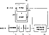
Among Fig. 1, terrestrial broadcasting, analog input, high definition TV (HDTV) signal are handled by the fan-in network 14 that comprises radio frequency (RF) tuning circuit and intermediate frequency (IF) module 16 that comprises the two frequency conversion tuning devices that produce the IF band output signal and suitable automatic gain control (AGC) circuit.The signal that receives is the suppressed carrier 8-VSB modulation signal that proposes and be applied to the U.S. as Major Leagues.Such VSB signal is by one-dimensional data code element group representation, and wherein only axle comprises the quantized data that will be recovered by receiver.For reduced graph 1, the signal that is used for illustrating synchronously functional block does not illustrate.
Be that the VSB transmission system uses the specified data frame format to transmit data described in the HDTV of the Major Leagues system specifications on April 14th, 1994 as the date.The little pilot signal that is arranged in the suppressed carrier frequency is added to the transmission signal, to help realizing carrier lock at the VSB receiving terminal.Each Frame comprises two, and every comprises 313 sections 832 multilevel code units.First section of every is called field synchronization segments, and remaining 312 sections are called data segment.Data segment typically comprises mpeg compatible (MPEG: packet active images expert group).Each data segment comprises that four code element sections accord with synchronously, is 828 data code elements subsequently.Each section comprises that four code element sections accord with synchronously, follows by the field synchronization component, comprises predetermined 511 code element pseudo random number (PN) sequences and three 63 predetermined code element PN sequences, and in the middle of it is reverse in continuous field.VSB mode control signal (definition VSB code element group size) is followed in the end after 63 PN sequences, is thereafter 96 standby code elements and 12 code elements of duplicating from previous field.
Then say Fig. 1, be converted to number of samples character code metadata streams by analog to digital converter (ADC) 19 from the frequency band IF output signal of IF module 16.From the output of ADC19 sampling digital data stream be demodulated to base band by all-digital demodulation device/carrier recovery network 22.This is to be finished by the little reference pilot carrier wave in the VSB data flow of all-digital phase-locked loop response reception.Unit 22 produces output I phase demodulating symbol data stream, describes in detail as reference Fig. 3.In addition, according to the present invention, unit 22 is connected with AGC controller 52 to produce IF and RF AGC signal.Be used to produce the apparatus and method of AGC signal below with reference to Fig. 2 and 4 explanations.
ADC19 uses the 21.52MHz sampling clock, i.e. the twice of receiving symbol speed is crossed sampling input 10.76M code element/second VSB symbol data and flowed, thereby provided sampling 21.52M data flow sampling/second with two sampling/code elements.This sampling based on two sampling/code elements handling, rather than based on the use of the sampling of the code element of handling one by one (a sampling/code element), produced favourable continuous signal and handled the enforcement of operation, such as the operation relevant with DC compensating unit 26 and NTSC (NTSC) interference detector 30.
The section of being that is connected with demodulator 22 with ADC19 synchronously and code element clock recovery network 24.Network 24 detects and the repeating data section synchronized component that separates each Frame from random data.Section be used to synchronously the to regenerate 21.52MHz clock of correct phasing, it is used to control the data flow code element sampling of analog to digital converter 19.Network 24 advantageously uses simplification dicode unit dependency basis quasi-mode to come detection segment synchronous with relevant dicode metadata correlator.
NTSC interweaves with detecting and suppress and is carried out by unit 30.Then, signal is by channel equalizer 34 adaptive equalizations, and this equalizer can be operated in conjunction with blindness, training and judgement instructional model.Equalizer 34 can be in the HDTV of the Major Leagues system specifications and the article " the VSB modem subsystem design of Major Leagues' digital television receiver " write of people such as IEEE consumer electronics journal W.Bretl in August nineteen ninety-five in the type of explanation.Equalizer also can be that sequence number is the type that illustrates in the U.S. Patent application of 09/102885 (RCA88,947).Before equalizer 34, come the output stream of self-detector 30 to be down-converted to the data flow of a sampling/code element (10.76M code element/second).This down-conversion can by suitable following sampling microwave network (for reduced graph 1 not shown) realize.
Demodulation in the unit 22 is controlled (APC) ring by digital automatic phase and is carried out, and recovers to realize carrier wave.Phase-locked loop uses weight of pilot frequency as the benchmark that initially obtains and be used for the standard phase discriminator that phase place obtains.Pilot signal be embedded in comprise show as at random, in the receiving data stream of the data of noise like pattern.Random data is ignored by the Filtering Processing that demodulator APC encircles basically.The 10.76M code element of ADC19/second input signal is that VSB frequency spectrum center is at 5.38MHz and weight of pilot frequency is positioned at the nearly baseband signal of 2.69MHz.Input traffic is crossed sampling by ADC19 with the 21.52MHz twice.Weight of pilot frequency has downconverted to DC in from the demodulated data stream of unit 22.
Fig. 3 shows the detail drawing of digital demodulator 22.8-VSB from ADC19 modulates, crosses number of samples character code metadata streams, comprises than the low frequency weight of pilot frequency, is applied to the input of Hilbert filter 320 and delay cell 322.Hilbert filter 320 is separated into " I " (homophase) and " Q " (quadrature phase) component with the IF sampled data stream of introducing.Postponing 322 provides and the consistent delay of Hilbert filter 320 delays.I and Q component use complex multiplier 324 to be converted into base band in the APC ring.In case loop is by synchronously, the output of multiplier 324 is exactly complex base band signal.From the output I data flow of multiplier 324 as the output of actual demodulation device, and be used for low pass filter 326 extract receiving data streams weight of pilot frequency.The phase place that is used to extract received signal from the output Q data flow of multiplier 324.
In the phase control ring, be applied to low pass filter 326 and 328 respectively from the I and the Q output signal of multiplier 324.Filter 326 and 328 is to have the Nyquist low pass filter that is about the 1MHz cut-off frequency, is used in unit 330 and 332 8: reduce signal bandwidth under 1 data before the sampling.Under take a sample Q signal by 336 filtering of automatic frequency control (AFC) filter.After the filtering, Q signal by unit 338 amplitude limits to reduce requirement to phase discriminator 340 dynamic ranges.Phase discriminator 340 detects and proofreaies and correct the I of the input that offers it and the phase difference between the Q signal, and produces the output phase error signal, and it is by APC filter 344 filtering of for example second-order low-pass filter.Represent near the expectation pilot signal frequency of DC and the frequency difference between the reception pilot signal frequency by the phase error that unit 340 detects.
If the reception pilot signal presents the expected frequency near DC, AFC unit 336 will not produce phase shift.The I and the Q passage weight of pilot frequency that input to phase discriminator 340 will present the deviation that does not have mutually orthogonal phase relation, and thus, phase discriminator 340 produces zero or near the phase error output signal of null value.But if receive the frequency that pilot signal presents mistake, AFC unit 336 will produce phase shift.This will cause using to the I of phase discriminator 340 inputs and the additional phase error between the Q passage pilot signal.Phase discriminator 340 these phase differences of response produce the output error value.
Because the following sampling of first front unit 330 and 332, the phase error signal of the filtering from 344 is by interpolater 346 1: sampling on 8, thus digital controlled oscillator (NCO) 348 is operated in 21.52MHz.The control input to NCO348 is used in the output of interpolater 346, and it is the local regeneration of demodulate reception data stream pilot signal.NCO348 comprises sinusoidal and cosine look-up table, is used to respond the phase control signal from unit 340,344 and 346, in correct phase place regeneration pilot tone.The output Be Controlled of NCO348 till the phase error signal that the I of multiplier 324 and Q signal output produce phase discriminator 340 is zero substantially, thereby represents that the baseband I signal of correct demodulation is presented on the output of multiplier 324.
In digital demodulator 22, main signal processing apparatus consists essentially of parts 336,338,340 and 344.The disposal ability and the hardware of demodulator has advantageously been saved in 8: 1 times samplings that provided by unit 330 and 332, and by making APC ring component 336,338,340 and 344 regularly on lower clock rate, for example use 21.52MHz/8 or 2.69MHz clock to replace the 21.52MHz clock, and realize treatment effeciency.Especially when digital signal processor (DSP) was used to realize network 22 and phase demodulation ring, described data reduced by for example suitably requiring less capable command code to bring software efficiency.DSP equipment loop can be used for other signal processing purpose.When application-specific IC (ASIC) when being used to realize network 22, the reduction of data brings the hardware and the Capability Requirement of reduction, and the integrated circuit surface that reduces is long-pending.Demodulator advantageously uses weight of pilot frequency to realize that carrier wave recovers, and has adopted feed-forward process by the decision data of amplitude limiter, rather than relative complex and feedback processing consuming time.
When multipath occurred in the ATSC signal, pilot tone might be decayed more than other frequency in the frequency spectrum.Phase-locked loop (PLL) is used to be locked to this pilot tone, so that have the relevant benchmark of VSB frequency spectrum heterodyne being reduced to base band at receiving terminal.Typically, this PLL can follow the tracks of than it the low level signal of signal that obtains.When the pilot drop that causes when multipath became quite serious, the automatic gain control circuit that acts on the whole VSB frequency spectrum may reach stable state, thus the energy that on pilot carrier frequency, does not just enough obtain.According to the present invention, be during carrier wave obtains, automatic gain control (AGC) to be used than the high reference power that uses during the remaining demodulation process to this way to solve the problem.This imports obtainable pilot energy at PLL during having increased the stage of obtaining.Therefore, this method makes pilot tone can successfully obtain under higher decay.After the PLL locking, the AGC reference power (magnification factor) that is applied to received signal can reduce according to the working range of residue demodulation block.
Fig. 2 shows the detail drawing that is used for carrying out according to the present invention the HDTV that carrier wave obtains.Fig. 4 shows and is used to carry out flow chart of the present invention.In order to understand the present invention best, the reader should be simultaneously with reference to Fig. 2 and 4.
More clearly, Fig. 2 has described the AGC controller 52 that comprises processor 202 and detector 204.Discuss with reference to Fig. 1 according to previous, AGC controller 52 is connected with RF tuner 14, IF tuner 16, ADC19 and carrier recovery network 22.Processor 202 is from the input equipment receiving inputted signal, and sets the reference power value in detector 204.Detector 204 benchmark performance numbers and from the base band of ADC19 or nearly base-band television signal, and produce the control signal that receives by IF module 16.
Respond this control signal, the agc circuit in the IF module 16 is adjusted the gain of IF module 16.When the power of base-band television signal was lower than the reference power value, control signal was set to and increases gain.When the power of base-band television signal was higher than the reference power value, control signal was set to and reduces gain.Like this, if the reference power value increases, input TV signal just is exaggerated.Similarly, if the reference power value reduces, input TV signal just is attenuated.Though the gain of IF module 16 has been discussed above, the gain of RF tuner 14 also can responsive control signal and is adjusted.
Fig. 4 shows the flow chart of carrying out the inventive method 400 is described in detail in detail.Method 400 starts in step 402, and wherein input signal is received at processor 202.Input signal can manually provide through button or certain input equipment (not shown), perhaps provides automatically when the software program of the pilot detection that realizes a period of time is carried out.Method 400 proceeds to step 404, and wherein processor 202 is set at high reference power value with the reference power value, such as the power that is higher than base-band television signal.Respond high reference power value, 204 pairs of IF modules of detector 16 increase the numerical value of control signal.When receiving the control signal numerical value of increase, the gain of IF module 16 is increased, thereby TV signal is amplified to first amplification level.The more important thing is that higher gain also increases the pilot energy of carrier recovery network 26, thereby realize that carrier wave obtains or obtaining pilot tone.
In step 406, processor 202 is from carrier recovery network 26 reception carrier locking signals.Method 400 proceeds to step 408, and wherein processor 202 is set at lower or normal reference power value with the reference power value, such as being lower than the TV signal that increases power in front.Normal reference power value is suitably set or is rule of thumb determined, is suitable for carrying out other demodulation, obtains or base-band television signal of the HDTV operation that other is discussed with reference to Fig. 1 so that provide.
Respond normal reference power value, 204 pairs of IF modules of detector 16 reduce control signal.When receiving the control signal of reduction, IF module 16 is amplified to second amplification level with TV signal.Because second amplification level is lower than first amplification level, the gain of IF module 16 is reduced.After step 408 was set lower reference power value, method 400 continued the remaining steady state operation with HDTV that obtains in step 410.
In case detect pilot tone, data-signal is that the usual manner that illustrates in 09/140,257 the U.S. Patent application is separated to be in harmonious proportion and handled with (RCA89,095) sequence number of submitting on August 26th, 1998.
Though the various embodiments in conjunction with the present invention instruction are shown specifically and illustrate at this, those skilled in the art can easily design many other still in conjunction with the embodiment of these instructions.
Claims (17)
1. method that the carrier wave that is used to carry out TV signal obtains, this signal has the pilot tone that is positioned at the carrier frequency center, and this method comprises:
Responsive control signal uses first amplification level to amplify described TV signal; With
From the TV signal of described amplification, obtain carrier frequency; With
After obtaining carrier frequency, use second amplification level to amplify described TV signal, wherein said first amplification level is greater than described second amplification level, and described first amplification level is enough to receiver is synchronized to described pilot tone.
2. method as claimed in claim 1, wherein the amplification of first step comprises the steps:
The reference power value is set at high numerical value; With
If described reference power value greater than the performance number of described TV signal, just increases the numerical value of described control signal, wherein use the amplification of described first amplification level to respond the added value of described control signal and take place.
3. method as claimed in claim 2, wherein said setting responds input command and takes place.
4. method as claimed in claim 1, wherein said obtaining comprises:
Detect described pilot tone from described TV signal.
5. method as claimed in claim 1, wherein saidly obtain later described amplification and comprise:
The reference power value is set at low numerical value, and described being set in obtained carrier frequency and provided later on;
If described reference power value less than the performance number of described TV signal, just reduces the numerical value of described control signal, wherein use the amplification of described second amplification level to respond the minimizing value of described control signal and take place.
6. method as claimed in claim 1, wherein the amplification of first step also comprises the steps:
Increase the gain of medium-frequency IF module.
7. method as claimed in claim 1, wherein saidly obtain later amplification and comprise:
Reduce the gain of medium-frequency IF module.
8. method as claimed in claim 1 further comprises:
When obtaining carrier frequency, produce the carrier lock signal, wherein use the amplification of described second amplification level to respond described carrier lock signal and take place.
9. method as claimed in claim 1, wherein said TV signal comprise the residual sideband VSB modulation signal that contains high-definition video data of reception.
10. device that the carrier wave that is used to carry out TV signal obtains, this signal has the pilot tone that is positioned at the carrier frequency center, and this device comprises:
Tuning circuit is used to use first amplification level to amplify described TV signal and use second amplification level amplifies described TV signal, and wherein said first amplification level is greater than described second amplification level;
Carrier recovery circuit is used for obtaining carrier frequency from the TV signal of described amplification; With
Control circuit, be connected with carrier recovery circuit with described tuner, be used to produce a control signal and produce described control signal later in described carrier recovery circuit reinsertion of carrier frequency, wherein said first amplification level is enough to described tuning circuit is synchronized to described pilot tone.
11. as the device of claim 10, wherein said control circuit comprises automatic gain control AGC controller.
12. as the device of claim 11, wherein said automatic gain control AGC controller comprises:
Processor is used for the reference power value is set at high numerical value; With
Detector, be connected with described processor, if described reference power value greater than the performance number of described TV signal, just increases the numerical value of described control signal, wherein said tuning circuit responds the added value of described control signal and uses described first amplification level to amplify described TV signal.
13. device as claim 12, wherein said processor is set at low numerical value with described reference power value after carrier frequency recovery, if and described reference power value is less than the performance number of described TV signal, described detector just reduces the numerical value of described control signal, and wherein said tuning circuit responds the minimizing value of described control signal and uses described second amplification level to amplify described TV signal.
14. as the device of claim 10, wherein said tuning circuit comprises the medium-frequency IF module.
15. as the device of claim 10, the gain of wherein said tuning circuit increases when receiving the added value of described control signal.
16. as the device of claim 10, the gain of wherein said tuning circuit reduces when receiving the minimizing value of described control signal.
17. as the device of claim 10, wherein said TV signal comprises the residual sideband VSB modulation signal that contains high-definition video data of reception.
Applications Claiming Priority (2)
| Application Number | Priority Date | Filing Date | Title |
|---|---|---|---|
| US14441399P | 1999-07-16 | 1999-07-16 | |
| US60/144413 | 1999-07-16 |
Publications (2)
| Publication Number | Publication Date |
|---|---|
| CN1361981A CN1361981A (en) | 2002-07-31 |
| CN1157943C true CN1157943C (en) | 2004-07-14 |
Family
ID=22508476
Family Applications (1)
| Application Number | Title | Priority Date | Filing Date |
|---|---|---|---|
| CNB008104735A Expired - Fee Related CN1157943C (en) | 1999-07-16 | 2000-07-13 | Selective gain adjustement to aid carrier acquisition in a high definition television receiver |
Country Status (10)
| Country | Link |
|---|---|
| EP (1) | EP1197077B8 (en) |
| JP (1) | JP4980528B2 (en) |
| KR (1) | KR100720983B1 (en) |
| CN (1) | CN1157943C (en) |
| AU (1) | AU5933000A (en) |
| DE (1) | DE60022755T2 (en) |
| MX (1) | MXPA02000555A (en) |
| MY (1) | MY128892A (en) |
| TW (1) | TW496084B (en) |
| WO (1) | WO2001006774A1 (en) |
Families Citing this family (8)
| Publication number | Priority date | Publication date | Assignee | Title |
|---|---|---|---|---|
| JP4554934B2 (en) * | 2002-01-11 | 2010-09-29 | アギア システムズ (アイルランド) リサーチ リミテッド | Timing control in data receivers and transmitters |
| KR100486269B1 (en) * | 2002-10-07 | 2005-04-29 | 삼성전자주식회사 | Carrier Recovery device for High definition television and method there of |
| KR100999493B1 (en) * | 2002-11-26 | 2010-12-09 | 톰슨 라이센싱 | A carrier tracking loop lock detector |
| CN1317875C (en) * | 2003-09-26 | 2007-05-23 | 南京Lg新港显示有限公司 | Carrier reset device |
| US7061276B2 (en) * | 2004-04-02 | 2006-06-13 | Teradyne, Inc. | Digital phase detector |
| FR2877181B1 (en) * | 2004-10-12 | 2014-05-30 | Samsung Electronics Co Ltd | Digital television receiver has phase compensator to offset phase of real and imaginary data based on phase offset signal and outputs phase adjusted data |
| TWI398166B (en) * | 2009-04-07 | 2013-06-01 | Himax Media Solutions Inc | Digital receiver and related method thereof |
| CN102724514B (en) * | 2012-05-16 | 2015-04-08 | 浙江大华技术股份有限公司 | Method and device for compensating transmission loss of analog video signal and equipment for receiving analog video signal |
Family Cites Families (3)
| Publication number | Priority date | Publication date | Assignee | Title |
|---|---|---|---|---|
| US5546138A (en) * | 1993-12-29 | 1996-08-13 | Zenith Electronics Corporation | AGC system with overriding, maximum gain during an initial interval to enhance signal acquisition |
| US5410368A (en) * | 1993-12-29 | 1995-04-25 | Zenith Electronics Corp. | Carrier acquisition by applying substitute pilot to a synchronous demodulator during a start up interval |
| US5627604A (en) * | 1994-04-04 | 1997-05-06 | Zenith Electronics Corporation | Stabilizing the lock up of a bi-phase stable FPLL by augmenting a recovered DC pilot |
-
2000
- 2000-07-13 MX MXPA02000555A patent/MXPA02000555A/en active IP Right Grant
- 2000-07-13 EP EP00945375A patent/EP1197077B8/en not_active Expired - Lifetime
- 2000-07-13 WO PCT/US2000/019134 patent/WO2001006774A1/en active IP Right Grant
- 2000-07-13 KR KR1020027000373A patent/KR100720983B1/en not_active IP Right Cessation
- 2000-07-13 DE DE60022755T patent/DE60022755T2/en not_active Expired - Lifetime
- 2000-07-13 JP JP2001511093A patent/JP4980528B2/en not_active Expired - Fee Related
- 2000-07-13 AU AU59330/00A patent/AU5933000A/en not_active Abandoned
- 2000-07-13 CN CNB008104735A patent/CN1157943C/en not_active Expired - Fee Related
- 2000-07-14 TW TW089114117A patent/TW496084B/en not_active IP Right Cessation
- 2000-07-14 MY MYPI20003243A patent/MY128892A/en unknown
Also Published As
| Publication number | Publication date |
|---|---|
| WO2001006774A1 (en) | 2001-01-25 |
| AU5933000A (en) | 2001-02-05 |
| MXPA02000555A (en) | 2002-07-02 |
| DE60022755T2 (en) | 2006-05-18 |
| EP1197077B8 (en) | 2005-11-30 |
| EP1197077A1 (en) | 2002-04-17 |
| MY128892A (en) | 2007-02-28 |
| EP1197077B1 (en) | 2005-09-21 |
| JP4980528B2 (en) | 2012-07-18 |
| JP2003505948A (en) | 2003-02-12 |
| KR20020024304A (en) | 2002-03-29 |
| DE60022755D1 (en) | 2005-10-27 |
| TW496084B (en) | 2002-07-21 |
| CN1361981A (en) | 2002-07-31 |
| KR100720983B1 (en) | 2007-05-23 |
Similar Documents
| Publication | Publication Date | Title |
|---|---|---|
| CN1166190C (en) | Digital symbol timing recovery network | |
| US6356598B1 (en) | Demodulator for an HDTV receiver | |
| US5818544A (en) | Method and apparatus for detecting when the carrier signal and symbol timing for a television signal is recovered and a high definition television employing the method and apparatus | |
| MXPA00010469A (en) | Demodulator for high-definition tv receiver. | |
| US20020105599A1 (en) | VSB demodulating device and method in digital TV receiver | |
| CN1143523C (en) | Co-channel interference detection network for HDTV receiver | |
| CN1229981C (en) | Gain contro lfor high definition television demodulator | |
| CN1157943C (en) | Selective gain adjustement to aid carrier acquisition in a high definition television receiver | |
| US6665355B1 (en) | Method and apparatus for pilot-aided carrier acquisition of vestigial sideband signal | |
| CN100589537C (en) | Channel aquisition method and device for a television receiver | |
| CN1208961C (en) | Controlled oscillator in network of digital character timing recovery | |
| Bretl et al. | VSB modem subsystem design for Grand Alliance digital television receivers | |
| CN1130899C (en) | Segment synchronous recovery network for HDTV receiver | |
| US6985192B1 (en) | Selective gain adjustment to aid carrier acquisition in a high definition television receiver | |
| CN1178485C (en) | High difinition television vestigial sideband receiver | |
| KR100508520B1 (en) | Apparatus and method for use in a system for processing a received vestigial sideband(vsb) modulated signal | |
| CN1187964C (en) | Network for eleiminating DC offset in a received HDTV signal | |
| KR100407975B1 (en) | Apparatus for recovering carrier | |
| KR100425104B1 (en) | Apparatus for recovering carrier | |
| KR100407976B1 (en) | Digital TV receiver | |
| KR100451741B1 (en) | Apparatus for recovering carrier | |
| MXPA00004216A (en) | Network for eliminating dc offset in a received hdtv signal | |
| KR20050063219A (en) | Vsb receiver and carrier recovery apparatus thereof | |
| MXPA01004216A (en) | Methods and compositions for the prevention of tolerance to medications |
Legal Events
| Date | Code | Title | Description |
|---|---|---|---|
| C06 | Publication | ||
| PB01 | Publication | ||
| C10 | Entry into substantive examination | ||
| SE01 | Entry into force of request for substantive examination | ||
| C14 | Grant of patent or utility model | ||
| GR01 | Patent grant | ||
| CF01 | Termination of patent right due to non-payment of annual fee |
Granted publication date: 20040714 Termination date: 20170713 |
|
| CF01 | Termination of patent right due to non-payment of annual fee |