CN115485580A - Monitoring signal chirp in LIDAR output signals - Google Patents
Monitoring signal chirp in LIDAR output signals Download PDFInfo
- Publication number
- CN115485580A CN115485580A CN202180035663.5A CN202180035663A CN115485580A CN 115485580 A CN115485580 A CN 115485580A CN 202180035663 A CN202180035663 A CN 202180035663A CN 115485580 A CN115485580 A CN 115485580A
- Authority
- CN
- China
- Prior art keywords
- signal
- lidar
- waveguide
- process variable
- frequency
- Prior art date
- Legal status (The legal status is an assumption and is not a legal conclusion. Google has not performed a legal analysis and makes no representation as to the accuracy of the status listed.)
- Pending
Links
Images


Classifications
-
- G—PHYSICS
- G01—MEASURING; TESTING
- G01S—RADIO DIRECTION-FINDING; RADIO NAVIGATION; DETERMINING DISTANCE OR VELOCITY BY USE OF RADIO WAVES; LOCATING OR PRESENCE-DETECTING BY USE OF THE REFLECTION OR RERADIATION OF RADIO WAVES; ANALOGOUS ARRANGEMENTS USING OTHER WAVES
- G01S17/00—Systems using the reflection or reradiation of electromagnetic waves other than radio waves, e.g. lidar systems
- G01S17/02—Systems using the reflection of electromagnetic waves other than radio waves
- G01S17/06—Systems determining position data of a target
- G01S17/08—Systems determining position data of a target for measuring distance only
- G01S17/32—Systems determining position data of a target for measuring distance only using transmission of continuous waves, whether amplitude-, frequency-, or phase-modulated, or unmodulated
- G01S17/34—Systems determining position data of a target for measuring distance only using transmission of continuous waves, whether amplitude-, frequency-, or phase-modulated, or unmodulated using transmission of continuous, frequency-modulated waves while heterodyning the received signal, or a signal derived therefrom, with a locally-generated signal related to the contemporaneously transmitted signal
-
- G—PHYSICS
- G01—MEASURING; TESTING
- G01S—RADIO DIRECTION-FINDING; RADIO NAVIGATION; DETERMINING DISTANCE OR VELOCITY BY USE OF RADIO WAVES; LOCATING OR PRESENCE-DETECTING BY USE OF THE REFLECTION OR RERADIATION OF RADIO WAVES; ANALOGOUS ARRANGEMENTS USING OTHER WAVES
- G01S7/00—Details of systems according to groups G01S13/00, G01S15/00, G01S17/00
- G01S7/48—Details of systems according to groups G01S13/00, G01S15/00, G01S17/00 of systems according to group G01S17/00
- G01S7/491—Details of non-pulse systems
- G01S7/4911—Transmitters
-
- G—PHYSICS
- G01—MEASURING; TESTING
- G01S—RADIO DIRECTION-FINDING; RADIO NAVIGATION; DETERMINING DISTANCE OR VELOCITY BY USE OF RADIO WAVES; LOCATING OR PRESENCE-DETECTING BY USE OF THE REFLECTION OR RERADIATION OF RADIO WAVES; ANALOGOUS ARRANGEMENTS USING OTHER WAVES
- G01S7/00—Details of systems according to groups G01S13/00, G01S15/00, G01S17/00
- G01S7/48—Details of systems according to groups G01S13/00, G01S15/00, G01S17/00 of systems according to group G01S17/00
- G01S7/491—Details of non-pulse systems
- G01S7/4912—Receivers
- G01S7/4913—Circuits for detection, sampling, integration or read-out
-
- G—PHYSICS
- G01—MEASURING; TESTING
- G01S—RADIO DIRECTION-FINDING; RADIO NAVIGATION; DETERMINING DISTANCE OR VELOCITY BY USE OF RADIO WAVES; LOCATING OR PRESENCE-DETECTING BY USE OF THE REFLECTION OR RERADIATION OF RADIO WAVES; ANALOGOUS ARRANGEMENTS USING OTHER WAVES
- G01S7/00—Details of systems according to groups G01S13/00, G01S15/00, G01S17/00
- G01S7/48—Details of systems according to groups G01S13/00, G01S15/00, G01S17/00 of systems according to group G01S17/00
- G01S7/491—Details of non-pulse systems
- G01S7/4912—Receivers
- G01S7/4917—Receivers superposing optical signals in a photodetector, e.g. optical heterodyne detection
-
- G—PHYSICS
- G01—MEASURING; TESTING
- G01S—RADIO DIRECTION-FINDING; RADIO NAVIGATION; DETERMINING DISTANCE OR VELOCITY BY USE OF RADIO WAVES; LOCATING OR PRESENCE-DETECTING BY USE OF THE REFLECTION OR RERADIATION OF RADIO WAVES; ANALOGOUS ARRANGEMENTS USING OTHER WAVES
- G01S7/00—Details of systems according to groups G01S13/00, G01S15/00, G01S17/00
- G01S7/48—Details of systems according to groups G01S13/00, G01S15/00, G01S17/00 of systems according to group G01S17/00
- G01S7/491—Details of non-pulse systems
- G01S7/4912—Receivers
- G01S7/4918—Controlling received signal intensity, gain or exposure of sensor
-
- G—PHYSICS
- G01—MEASURING; TESTING
- G01S—RADIO DIRECTION-FINDING; RADIO NAVIGATION; DETERMINING DISTANCE OR VELOCITY BY USE OF RADIO WAVES; LOCATING OR PRESENCE-DETECTING BY USE OF THE REFLECTION OR RERADIATION OF RADIO WAVES; ANALOGOUS ARRANGEMENTS USING OTHER WAVES
- G01S7/00—Details of systems according to groups G01S13/00, G01S15/00, G01S17/00
- G01S7/48—Details of systems according to groups G01S13/00, G01S15/00, G01S17/00 of systems according to group G01S17/00
- G01S7/499—Details of systems according to groups G01S13/00, G01S15/00, G01S17/00 of systems according to group G01S17/00 using polarisation effects
Abstract
A LIDAR system includes at least one optical component configured to output a system output signal that travels away from the LIDAR system and may be reflected by objects located outside the LIDAR system. The LIDAR system also includes a control mechanism configured to control one or more process variables of the system output signal. The control mechanism uses the electrical process variable signal to control the process variable. The process variable signal has an in-phase component and a quadrature component.
Description
RELATED APPLICATIONS
This application is a continuation of U.S. patent application No. 16/875,987, filed on 16/5/2020, entitled "MONITORING SIGNAL CHIRP IN LIDAR OUTPUT SIGNALS," and incorporated in its entirety.
Technical Field
The present invention relates to optical devices. In particular, the present invention relates to LIDAR systems.
Background
There is an increasing commercial demand for LIDAR systems that can be deployed in applications such as ADAS (advanced driver assistance systems) and AR (augmented reality). LIDAR (light detection and ranging) systems typically output a system output signal that is reflected by an object located outside the LIDAR system. At least a portion of the reflected light signal is returned to the LIDAR system. The LIDAR system directs the received light signal to a light sensor, which converts the light signal to an electrical signal. The electronics can use the light sensor output to quantify LIDAR data indicative of radial velocity and/or distance between the object and the LIDAR system.
Many LIDAR systems tune the frequency of the system output signal linearly or with other well-defined waveforms versus time to enable accurate measurements of the LIDAR data. In these examples, the LIDAR system may monitor the frequency of the system output signal and tune the frequency in response to the monitored frequency to achieve a desired waveform shape. Systems for monitoring the frequency of the system output signal may require one or more waveguides that need to be undesirably long in order to achieve the desired result. Due to this waveguide length, these systems typically occupy a large portion of the available space on the LIDAR chip. Accordingly, there is a need for an improved system for monitoring the frequency of a LIDAR system output signal.
Disclosure of Invention
A LIDAR system includes at least one optical component configured to output a system output signal that travels away from the LIDAR system and may be reflected by objects located outside the LIDAR system. The LIDAR system also includes a control mechanism configured to control one or more process variables of the system output signal. The control mechanism uses the electrical process variable signal to control a process variable. The process variable signal has an in-phase component and a quadrature component.
Drawings
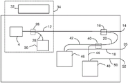
Fig. 1A is a top view of a schematic diagram of a LIDAR system including or consisting of a LIDAR chip that outputs LIDAR output signals and receives LIDAR input signals on a common waveguide.
Fig. 1B is a top view of a schematic diagram of a LIDAR system that includes or consists of a LIDAR chip that outputs a LIDAR output signal and receives a LIDAR input signal on a different waveguide.
Fig. 1C is a top view of a schematic diagram of another embodiment of a LIDAR system including or consisting of a LIDAR chip that outputs a LIDAR output signal and receives multiple LIDAR input signals on different waveguides.
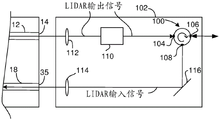
Fig. 2 is a top view of an example LIDAR adapter suitable for use with the LIDAR chip of fig. 1B.
Fig. 3 is a top view of an example LIDAR adapter suitable for use with the LIDAR chip of fig. 1C.
Fig. 4 is a top view of an example of a LIDAR system including the LIDAR chip of fig. 1A and the LIDAR adapter of fig. 2 on a common support.
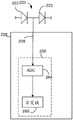
Fig. 5A illustrates an example of a processing component suitable for use in a LIDAR system.
Fig. 5B provides a schematic diagram of electronics suitable for use in a processing assembly constructed in accordance with fig. 5A.
Fig. 5C is a plot of frequency versus time for a system output signal with triangular frequency tuning.
Fig. 5D illustrates another example of a processing component suitable for use in a LIDAR system.
Fig. 5E provides a schematic diagram of an electronic device suitable for use with a processing assembly constructed in accordance with fig. 5D.
Fig. 6A and 6B illustrate examples of suitable control components for use as all or part of the control components disclosed in the context of fig. 1A-1C. Fig. 6A illustrates an interface between an optical component and a light sensor that may be positioned on a LIDAR chip.
Fig. 6B is a schematic diagram of the relationship between electronics and a light sensor that may be included on a LIDAR chip.
Fig. 6C is a graph showing the amplitude of the in-phase and quadrature components of the signal on the same time axis versus the frequency of the system output signal.
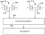
FIG. 6D illustrates one example of a process variable identification component suitable for use in an electronic device of a LIDAR system.
Fig. 6E illustrates another example of a process variable identification component suitable for use in an electronic device of a LIDAR system.
Fig. 7 is a cross-section of a portion of a LIDAR chip that includes a waveguide on a silicon-on-insulator platform.
Detailed Description
A LIDAR system includes a control mechanism configured to control a process variable of a system output signal. In some examples, the control mechanism is a control loop, such as a feedback control loop. The system output signal is a light signal that is output by the LIDAR system and then returned to the LIDAR system after being reflected by an object located outside of the LIDAR system. The LIDAR system may then use the reflected light to generate LIDAR data for the object. Examples of process variables that can be controlled by a control mechanism include the frequency and/or phase of the system output signal.
The control mechanism generates a control signal that carries data indicative of a value of a process variable. The control signal is generated from a process variable signal that includes an in-phase component and a quadrature component. The process variable signal is beat-generated due to the contributions from the signals at different frequencies. The use of a quadrature component allows the frequency of the control signal to be increased relative to the frequency of the control signal that would be generated if the process variable signal included only an in-phase component. Increasing the frequency of the control signal reduces the beat frequency of the process variable signal required to determine the value of the process variable. In prior systems, the beat frequency was increased by increasing the length of one waveguide in the mach-zehnder interferometer. The quadrature component also reduces the length required for one of the waveguides in the mach-zehnder interferometer, since the quadrature component reduces the required beat frequency. Thus, the orthogonal component may reduce the amount of space on the LIDAR chip occupied by the control mechanism.
Fig. 1A is a top view of a schematic diagram of a LIDAR chip that may be used as a LIDAR system or may be included in a LIDAR system that includes components in addition to the LIDAR chip. The LIDAR chip may include a Photonic Integrated Circuit (PIC), and may be a photonic integrated circuit chip. The LIDAR chip comprises a light source 4 which outputs a preliminary outgoing LIDAR signal. Suitable light sources 4 include, but are not limited to, semiconductor lasers such as External Cavity Lasers (ECL), distributed feedback lasers (DFB), discrete Mode (DM) lasers, and distributed bragg reflector lasers (DBR).
The LIDAR chip comprises a utility waveguide 12, which utility waveguide 12 receives an outgoing LIDAR signal from the light source 4. The utility waveguide 12 terminates at a facet (facet) 14 and carries the outgoing LIDAR signal to the facet 14. The facet 14 may be positioned such that an outgoing LIDAR signal passing through the facet 14 exits the LIDAR chip and is used as a LIDAR output signal. For example, the facet 14 may be positioned at the edge of the chip such that the outgoing LIDAR signals passing through the facet 14 exit the chip and are used as LIDAR output signals. In some instances, the portion of the LIDAR output signal that has exited from the LIDAR chip may also be considered the system output signal. As an example, when the departure of a LIDAR output signal from a LIDAR chip is also a departure of a LIDAR output signal from a LIDAR system, the LIDAR output signal may also be considered a system output signal.
The LIDAR output signals travel away from the LIDAR system through free space in the atmosphere in which the LIDAR system is located. The LIDAR output signal may be reflected by one or more objects in the LIDAR output signal path. When the LIDAR output signal is reflected, at least a portion of the reflected light travels back toward the LIDAR chip as the LIDAR input signal. In some instances, the LIDAR input signal may also be considered a system return signal. As an example, a LIDAR input signal may also be considered a system return signal when the departure of a LIDAR output signal from a LIDAR chip is also a departure of a LIDAR output signal from a LIDAR system.
The LIDAR input signal may enter the utility waveguide 12 through a facet 14. The portion of the LIDAR input signal that enters the utility waveguide 12 serves as an incident LIDAR signal. The utility waveguide 12 carries the incoming LIDAR signal to a splitter 16, the splitter 16 moving a portion of the outgoing LIDAR signal from the utility waveguide 12 as a comparison signal onto a comparison waveguide 18. The comparison waveguide 18 carries the comparison signal to the processing component 22 for further processing. Although fig. 1A illustrates a directional coupler operating as splitter 16, other signal splitting components may also be used as splitter 16. Suitable splitters 16 include, but are not limited to, directional couplers, optical couplers, y-junctions, tapered couplers, and multi-mode interference (MMI) devices.
The utility waveguide 12 also carries the outgoing LIDAR signal to a splitter 16. The splitter 16 moves a portion of the outgoing LIDAR signal from the utility waveguide 12 onto the reference waveguide 20 as a reference signal. The reference waveguide 20 carries the reference signal to a processing component 22 for further processing.
The percentage of light transmitted by the splitter 16 from the utility waveguide 12 can be fixed or substantially fixed. For example, the splitter 16 may be configured such that the power of the reference signal delivered to the reference waveguide 20 is the outgoing percentage of the power of the outgoing LIDAR signal, or such that the power of the comparison signal delivered to the comparison waveguide 18 is the incoming percentage of the power of the incoming LIDAR signal. In many splitters 16, such as directional couplers and multimode interferometers (MMIs), the exit percentage is equal or substantially equal to the entrance percentage. In some examples, the percentage of exit is greater than 30%,40% or 49% and/or less than 51%, 60% or 70% and/or the percentage of entry is greater than 30%,40% or 49% and/or less than 51%, 60% or 70%. The splitter 16, such as a multimode interferometer (MMI), typically provides an exit percentage and an entrance percentage of 50% or about 50%. However, multimode interferometers (MMIs) are easier to manufacture in platforms such as silicon-on-insulator platforms than certain alternatives. In one example, the splitter 16 is a multi-mode interferometer (MMI) and the exit and entrance percentages are 50% or substantially 50%. As will be described in more detail below, the processing component 22 combines the comparison signal with the reference signal to form a composite signal that carries LIDAR data for the sample region over the field of view. Thus, the composite signal may be processed in order to extract LIDAR data (radial velocity and/or distance between the LIDAR system and an object external to the LIDAR system) for the sample region.
The LIDAR chip may comprise a control branch for controlling the operation of the light source 4. The control branch comprises a splitter 26, the splitter 26 moving a portion of the outgoing LIDAR signal from the utility waveguide 12 onto a control waveguide 28. The coupled portion of the outgoing LIDAR signal serves as a tap signal. Although fig. 1A illustrates a directional coupler operating as splitter 26, other signal splitting components may be used as splitter 26. Suitable splitters 26 include, but are not limited to, directional couplers, optical couplers, y-junctions, tapered couplers, and multi-mode interference (MMI) devices.
The LIDAR system may be modified such that the incoming LIDAR signal and the outgoing LIDAR signal may be carried on different waveguides. For example, fig. 1B is a top view of the LIDAR chip of fig. 1A modified such that the incoming LIDAR signals and the outgoing LIDAR signals are carried on different waveguides. The outgoing LIDAR signal exits the LIDAR chip through the facet 14 and is used as a LIDAR output signal. When light from the LIDAR output signal is reflected by an object external to the LIDAR system, at least a portion of the reflected light is returned to the LIDAR chip as the first LIDAR input signal. The first LIDAR input signal enters the comparison waveguide 18 through facet 35 and is used as a comparison signal. The comparison waveguide 18 carries the comparison signal to the processing component 22 for further processing. As described in the context of fig. 1A, the reference waveguide 20 carries the reference signal to the processing component 22 for further processing. As will be described in more detail below, the processing component 22 combines the comparison signal with the reference signal to form a composite signal that carries LIDAR data for the sample region over the field of view.
The LIDAR chip may be modified to receive multiple LIDAR input signals. For example, fig. 1C illustrates the LIDAR chip of fig. 1B modified to receive two LIDAR input signals. The splitter 40 is configured to place a portion of the reference signal carried on the reference waveguide 20 on a first reference waveguide 42 and another portion of the reference signal on a second reference waveguide 44. Thus, the first reference waveguide 44 carries a first reference signal and the second reference guided wave 44 carries a second reference signal. The first reference waveguide 42 carries the first reference signal to a first processing component 46 and the second reference waveguide 44 carries the second reference signal to a second processing component 48. Examples of suitable splitters 40 include, but are not limited to, y-junctions, optical couplers, and multi-mode interference couplers (MMIs).
The outgoing LIDAR signal exits the LIDAR chip through the facet 14 and is used as a LIDAR output signal. When light from the LIDAR output signal is reflected by one or more objects located outside the LIDAR system, at least a portion of the reflected light is returned to the LIDAR chip as the first LIDAR input signal. The first LIDAR input signal enters the comparison waveguide 18 through the cut facet 35 and serves as a first comparison signal. The comparison waveguide 18 carries the first comparison signal to the first processing component 46 for further processing.
Further, when light from the LIDAR output signal is reflected by one or more objects located outside of the LIDAR system, at least a portion of the reflected signal is returned to the LIDAR chip as a second LIDAR input signal. The second LIDAR input signal enters the second comparison waveguide 50 through the facet 52 and is used as a second comparison signal carried by the second comparison waveguide 50. The second comparison waveguide 50 carries the second comparison signal to the second processing assembly 48 for further processing.
Although the light source 4 is shown as being located on the LIDAR chip, the light source 4 may be located outside the LIDAR chip. For example, the utility waveguide 12 may terminate at a second facet through which outgoing LIDAR signals may enter the utility waveguide 12 from a light source 4 located off-chip.
In some examples, a LIDAR chip constructed according to fig. 1B or fig. 1C is used in conjunction with a LIDAR adapter. In some instances, the LIDAR adapter may be physically optically positioned between the LIDAR chip and the one or more reflective objects and/or the field of view because an optical path of the first LIDAR input signal(s) and/or the LIDAR output signal traveling from the LIDAR chip to the field of view passes through the LIDAR adapter. Further, the LIDAR adapter may be configured to operate on the first LIDAR input signal and the LIDAR output signal such that the first LIDAR input signal and the LIDAR output signal travel on different optical paths between the LIDAR adapter and the LIDAR chip, but travel on the same optical path between the LIDAR adapter and a reflective object in the field of view.
An example of a LIDAR adapter suitable for use with the LIDAR chip of fig. 1B is illustrated in fig. 2. The LIDAR adapter includes a plurality of components positioned on a base. For example, the LIDAR adapter includes a circulator 100 positioned on a base 102. The optical circulator 100 shown includes three ports and is configured such that light entering one port exits the next port. For example, the illustrated optical circulator includes a first port 104, a second port 106, and a third port 108. The LIDAR output signal enters the first port 104 from the utility waveguide 12 of the LIDAR chip and exits from the second port 106.
The LIDAR adapter may be configured such that an output of the LIDAR output signal from the second port 106 may also be used as an output of the LIDAR output signal from the LIDAR adapter (and correspondingly from the LIDAR system). As a result, a LIDAR output signal may be output from the LIDAR adapter such that the LIDAR output signal travels toward the sample region in the field of view. Thus, in some instances, portions of the LIDAR output signal that have exited from the LIDAR adapter may also be considered system output signals. As an example, when the departure of a LIDAR output signal from a LIDAR adapter is also a departure of a LIDAR output signal from a LIDAR system, the LIDAR output signal may also be considered a system output signal.
The LIDAR output signal output from the LIDAR adapter comprises, consists of, or consists essentially of light from the LIDAR output signal received from the LIDAR chip. Accordingly, the LIDAR output signals output from the LIDAR adapter may be the same or substantially the same as the LIDAR output signals received from the LIDAR chip. However, there may be a difference between the LIDAR output signals output from the LIDAR adapter and the LIDAR output signals received from the LIDAR chip. For example, the LIDAR adapter may experience optical loss as the LIDAR output signal travels through the LIDAR adapter, and/or the LIDAR adapter may optionally include an amplifier configured to amplify the LIDAR output signal as it travels through the LIDAR adapter.
When one or more objects in the sample region reflect the LIDAR output signal, at least a portion of the reflected light travels back to the circulator 100 as a system return signal. The system return signal enters circulator 100 through second port 106. Fig. 2 illustrates that the LIDAR output signal and the system return signal travel along the same optical path between the LIDAR adapter and the sample region.
The system return signal exits circulator 100 through third port 108 and is directed to comparison waveguide 18 on the LIDAR chip. Thus, all or a portion of the system return signal may be used as the first LIDAR input signal, and the first LIDAR input signal comprises or consists of light from the system return signal. Thus, the LIDAR output signal and the first LIDAR input signal travel along different optical paths between the LIDAR adapter and the LIDAR chip.
As is clear from fig. 2, the LIDAR adapter may include an optical component in addition to the circulator 100. For example, the LIDAR adapter may include components for directing and controlling the optical paths of the LIDAR output signals and the system return signals. As an example, the adapter of fig. 2 includes an optional amplifier 110 positioned to receive and amplify the LIDAR output signal before it enters the circulator 100. The amplifier 110 may be operated by the electronics 32, allowing the electronics 32 to control the power of the LIDAR output signal.
Fig. 2 also illustrates that the LIDAR adapter includes an optional first lens 112 and an optional second lens 114. The first lens 112 may be configured to couple the LIDAR output signals to a desired location. In some instances, the first lens 112 is configured to focus or collimate the LIDAR output signal at a desired location. In one example, when the LIDAR adapter does not include the amplifier 110, the first lens 112 is configured to couple the LIDAR output signal on the first port 104. As another example, when the LIDAR adapter includes the amplifier 110, the first lens 112 may be configured to couple the LIDAR output signal to the amplifier 110 on the inlet port. The second lens 114 may be configured to couple the LIDAR output signal at a desired location. In some instances, the second lens 114 is configured to focus or collimate the LIDAR output signal at a desired location. For example, the second lens 114 may be configured to couple the LIDAR output signal onto the cleaved facet 35 of the comparison waveguide 18.
The LIDAR adapter may also include one or more direction changing components, such as a mirror. Fig. 2 illustrates that the LIDAR adapter includes a mirror as a direction change component 116 that redirects the system return signal from the circulator 100 to the cleaved facet 20 of the comparison waveguide 18.
The LIDAR chip includes one or more waveguides that constrain the optical path of one or more optical signals. While the LIDAR adapter may include a waveguide, the optical path traveled by the system return signal and the LIDAR output signal between components on the LIDAR adapter and/or between the LIDAR chip and components on the LIDAR adapter may be free space. For example, the system return signals and/or the LIDAR output signals may pass through the LIDAR chip, the LIDAR adapter, and/or the atmosphere in which the base 102 is located while traveling between different components on the LIDAR adapter and/or between a component on the LIDAR adapter and the LIDAR chip. As a result, optical components, such as lenses and direction changing components, may be employed to control the characteristics of the optical path that the system return signal and the LIDAR output signal travel on, to, and from the LIDAR adapter.
The LIDAR system may be configured to compensate for polarization. Light from the laser source is typically linearly polarized, and thus the LIDAR output signal is also typically linearly polarized. Reflection from the object can change the polarization angle of the returning light. Thus, the system return signal may comprise light of different linear polarization states. For example, a first portion of the system return signal may include light of a first linear polarization state and a second portion of the system return signal may include light of a second linear polarization state. The strength of the resulting composite signal is proportional to the square of the cosine of the angle between the comparison signal polarization field and the reference signal polarization field. If the angle is 90 degrees, the LIDAR data may be lost in the resulting composite signal. However, the LIDAR system may be modified to compensate for changes in the polarization state of the LIDAR output signal.
Fig. 3 illustrates the LIDAR system of fig. 3 modified such that the LIDAR adapter is suitable for use with the LIDAR chip of fig. 1C. The LIDAR adapter includes a beam splitter 120 that receives the system return signal from the circulator 100. The beam splitter 120 splits the system return signal into a first portion of the system return signal and a second portion of the system return signal. Suitable beam splitters include, but are not limited to, wollaston prisms and MEMS-based beam splitters.
A first portion of the system return signal is directed to comparison waveguide 18 on the LIDAR chip and used as the first LIDAR input signal described in the context of fig. 1C. A second portion of the system return signal is directed to polarization rotator 122. The polarization rotator 122 outputs a second LIDAR input signal that is directed to a second input waveguide 76 on the LIDAR chip and used as the second LIDAR input signal.
The beam splitter 120 may be a polarizing beam splitter. One example of a polarizing beam splitter is configured such that a first portion of the system return signal has a first polarization state but no or substantially no second polarization state, and a second portion of the system return signal has a second polarization state but no or substantially no first polarization state. The first and second polarization states may be linear polarization states, and the second polarization state is different from the first polarization state. For example, the first polarization state may be TE and the second polarization state may be TM, or the first polarization state may be TM and the second polarization state may be TE. In some instances, the laser source may be linearly polarized such that the LIDAR output signal has a first polarization state. Suitable beam splitters include, but are not limited to, wollaston prisms and MEM-based polarizing beam splitters.
The polarization rotator may be configured to change a polarization state of the first portion of the system return signal and/or the second portion of the system return signal. For example, the polarization rotator 122 shown in fig. 3 may be configured to change the polarization state of the second portion of the system return signal from the second polarization state to the first polarization state. As a result, the second LIDAR input signal has the first polarization state, but no or substantially no second polarization state. Thus, the first and second LIDAR input signals each have the same polarization state (in this example, the first polarization state). Although carrying light of the same polarization state, the first and second LIDAR input signals are associated with different polarization states due to the use of the polarizing beam splitter. For example, a first LIDAR input signal carries light reflected in a first polarization state, and a second LIDAR input signal carries light reflected in a second polarization state. As a result, the first LIDAR input signal is associated with a first polarization state and the second LIDAR input signal is associated with a second polarization state.
Since the first LIDAR input signal and the second LIDAR carry light of the same polarization state, the comparison signal generated from the first LIDAR input signal has the same polarization angle as the comparison signal generated from the second LIDAR input signal.
Suitable polarization rotators include, but are not limited to, rotation of polarization maintaining fibers, faraday rotators, half-wave plates, MEM-based polarization rotators, and integrated optical polarization rotators using asymmetric y-branches, mach-zehnder interferometers, and multimode interference couplers.
Since the outgoing LIDAR signal is linearly polarized, the first reference signal may have the same linear polarization state as the second reference signal. Further, components on the LIDAR adapter may be selected such that the first reference signal, the second reference signal, the comparison signal, and the second comparison signal each have the same polarization state. In the example disclosed in the context of fig. 3, the first comparison signal, the second comparison signal, the first reference signal, and the second reference signal may each have light of a first polarization state.
As a result of the above-described configuration, the first composite signal generated by the first processing component 46 and the second composite signal generated by the second processing component 48 each result from combining the reference signal and the comparison signal of the same polarization state, and will accordingly provide the desired beat between the reference signal and the comparison signal. For example, the composite signal results from combining the first reference signal and the first comparison signal of the first polarization state and excluding or substantially excluding light of the second polarization state, or the composite signal results from combining the first reference signal and the first comparison signal of the second polarization state and excluding or substantially excluding light of the first polarization state. Similarly, the second composite signal comprises a second reference signal and a second comparison signal of the same polarization state, which will accordingly provide the desired beat between the reference signal and the comparison signal. For example, the second composite signal results from combining the second reference signal and the second comparison signal in the first polarization state and excluding or substantially excluding light in the second polarization state, or the second composite signal results from combining the second reference signal and the second comparison signal in the second polarization state and excluding or substantially excluding light in the first polarization state.
The above-described configuration results in LIDAR data for a single sample region in the field of view being generated from a plurality of different composite signals (i.e., a first composite signal and a second composite signal) from the sample region. In some examples, determining the LIDAR data for the sample region includes the electronics combining the LIDAR data from different composite signals (i.e., the composite signal and the second composite signal). Combining the LIDAR data may include acquiring an average, median, or pattern of the LIDAR data generated from the different composite signals. For example, the electronic device may average the distance between the LIDAR system and the reflective object determined from the composite signal with the distance determined from the second composite signal, and/or the electronic device may average the radial velocity between the LIDAR system and the reflective object determined from the composite signal with the radial velocity determined from the second composite signal.
In some examples, determining the LIDAR data for the sample region includes the electronics identifying the one or more composite signals (i.e., the composite signal and/or the second composite signal) as being the source that best represents the real-world LIDAR data (representative LIDAR data). The electronic device may then use the LIDAR data from the identified composite signal as representative LIDAR data for additional processing. For example, the electronic device may identify a signal with a larger amplitude (the composite signal or the second composite signal) as representative LIDAR data and may use the LIDAR data from the identified signal for further processing by the LIDAR system. In some examples, an electronic device combines the following operations: a composite signal with representative LIDAR data is identified and LIDAR data from different LIDAR signals is combined. For example, the electronic device may identify each composite signal having an amplitude above an amplitude threshold as representative LIDAR data, and when more than two composite signals are identified as representative LIDAR data, the electronic device may combine the LIDAR data from each identified composite signal. When a composite signal is identified as having representative LIDAR data, the electronic device may use the LIDAR data from the composite signal as representative LIDAR data. When none of the composite signals are identified as having representative LIDAR data, the electronics can discard the LIDAR data for the sample regions associated with those composite signals.
Although FIG. 3 is described in the following context: the assembly is arranged such that the first comparison signal, the second comparison signal, the first reference signal and the second reference signal each have a first polarisation state, but other configurations of the assembly in figure 3 may be arranged such that a composite signal results from combining the reference signal and the comparison signal of the same linear polarisation state, and a second composite signal results from combining the reference signal and the comparison signal of the same linear polarisation state. For example, the beam splitter 120 can be configured such that the second portion of the system return signal has a first polarization state and the first portion of the system return signal has a second polarization state, the polarization rotator receives the first portion of the system return signal, and the outgoing LIDAR signal can have the second polarization state. In this example, the first and second LIDAR input signals each have a second polarization state.
The above-described system configuration results in the first portion of the system return signal and the second portion of the system return signal being directed to different composite signals. As a result, the LIDAR system compensates for changes in the polarization state of the LIDAR output signal in response to reflections of the LIDAR output signal because the first portion of the system return signal and the second portion of the system return signal are each associated with a different polarization state, but the electronics can process each composite signal.
The LIDAR adapter of fig. 3 may include additional optical components, including passive optical components. For example, the LIDAR adapter may include an optional third lens 126. The third lens 126 may be configured to couple the second LIDAR output signal at a desired location. In some examples, the third lens 126 focuses or collimates the second LIDAR output signal at a desired position. For example, the third lens 126 may be configured to focus or collimate the second LIDAR output signal onto the cleaved facet 52 of the second comparison waveguide 50. The LIDAR adapter also includes one or more direction changing components 124, such as mirrors and prisms. Fig. 3 illustrates that the LIDAR adapter includes a mirror as the direction change component 124, which direction change component 124 redirects a second portion of the system return signal from the circulator 100 to the cleaved facet 52 of the second comparison waveguide 50 and/or to the third lens 126.
When the LIDAR system includes a LIDAR chip and a LIDAR adapter, the LIDAR chip, the electronics, and the LIDAR adapter may be positioned on a common mount. Suitable common mounting portions include, but are not limited to, glass plates, metal plates, silicon plates, and ceramic plates. By way of example, fig. 4 is a top view of a LIDAR system that includes the LIDAR chip and electronics 32 of fig. 1A and the LIDAR adapter of fig. 2 on a common mount 140. Although the electronic device 32 is shown on a common support, all or a portion of the electronic device may be located outside of the common support. When the light source 4 is located outside the LIDAR chip, the light source may be located on the common support 140 or outside the common support 140. Suitable methods of mounting the LIDAR chip, electronics, and/or LIDAR adapter on the common support include, but are not limited to, epoxy, solder, and mechanical clamping.
LIDAR systems may include components including additional passive and/or active optical components. For example, a LIDAR system may include one or more components that receive LIDAR output signals from a LIDAR chip or a LIDAR adapter. Portions of the LIDAR output signal exiting from one or more components may be used as system output signals. As an example, a LIDAR system may include one or more beam steering components that receive LIDAR output signals from a LIDAR chip or LIDAR adapter and output all or a portion of the LIDAR output signals for use as system output signals. For example, fig. 4 illustrates a beam steering component 142 that receives LIDAR output signals from a LIDAR adapter. Although fig. 4 shows the beam steering assembly positioned on the common support 140, the beam steering assembly may be positioned on the LIDAR chip, on the LIDAR adapter, off the LIDAR chip, or off the common support 140. Suitable beam steering components include, but are not limited to, movable mirrors, MEMS mirrors, optical Phased Arrays (OPAs) and actuators that move the LIDAR chip, LIDAR adapters and/or common supports.
The electronics can operate one or more beam steering assemblies 142 to steer the system output signal to different sample regions 144. The sample region may extend away from the LIDAR system to a maximum distance for which the LIDAR system is configured to provide reliable LIDAR data. The sample regions may be woven together to define the field of view. For example, the field of view of the LIDAR system includes or consists of the space occupied by the sample area combination.
Fig. 5A-5C illustrate examples of suitable processing assemblies for use as all or a portion of the processing assembly selected from the group consisting of the processing assembly 22, the first processing assembly 46, and the second processing assembly 48. The processing component receives a comparison signal from a comparison waveguide 196 and a reference signal from a reference waveguide 198. The comparison waveguide 18 and the reference waveguide 20 shown in fig. 1A and 1B may be used as the comparison waveguide 196 and the reference waveguide 198, the comparison waveguide 18 and the first reference waveguide 42 shown in fig. 1C may be used as the comparison waveguide 196 and the reference waveguide 198, or the second comparison waveguide 50 and the second reference waveguide 44 shown in fig. 1C may be used as the comparison waveguide 196 and the reference waveguide 198.
The processing assembly includes a second splitter 200 that splits the comparison signal carried on the comparison waveguide 196 onto a first comparison waveguide 204 and a second comparison waveguide 206. The first comparison waveguide 204 carries a first portion of the comparison signal to an optical combining component 211. The second comparison waveguide 208 carries a second portion of the comparison signal to a second optical combining component 212.
The processing assembly includes a first splitter 202 that splits the reference signal carried on the reference waveguide 198 onto a first reference waveguide 204 and a second reference waveguide 206. First reference waveguide 204 carries a first portion of the reference signal to optical combining component 211. The second reference waveguide 208 carries a second portion of the reference signal to a second optical combining component 212.
The second optical combining component 212 combines the second portion of the comparison signal and the second portion of the reference signal into a second composite signal. The second composite signal produces a beat between the second portion of the comparison signal and the second portion of the reference signal due to a frequency difference between the second portion of the comparison signal and the second portion of the reference signal.
The second optical combining component 212 also splits the resulting second composite signal onto a first auxiliary detector waveguide 214 and a second auxiliary detector waveguide 216. The first auxiliary detector waveguide 214 carries the first portion of the second composite signal to the first auxiliary photosensor 218, and the first auxiliary photosensor 218 converts the first portion of the second composite signal to a first auxiliary electrical signal. The second auxiliary detector waveguide 216 carries a second portion of the second composite signal to a second auxiliary photosensor 220, the second auxiliary photosensor 220 converting the second portion of the second composite signal to a second auxiliary electrical signal. Examples of suitable photosensors include germanium Photodiodes (PDs) and Avalanche Photodiodes (APDs).
In some examples, the second optical combining component 212 separates the second composite signal such that a portion of the comparison signal included in the first portion of the second composite signal (i.e., a portion of the second portion of the comparison signal) is phase shifted 180 degrees relative to a portion of the comparison signal included in the second portion of the second composite signal (i.e., a portion of the second portion of the comparison signal) 0 But the portion of the reference signal in the second portion of the second composite signal (i.e., the portion of the second portion of the reference signal) is not phase shifted relative to the portion of the reference signal in the first portion of the second composite signal (i.e., the portion of the second portion of the reference signal). Alternatively, the second optical combining component 212 separates the second composite signal such that the portion of the reference signal in the first portion of the second composite signal (i.e., the portion of the second portion of the reference signal) is phase shifted 180 degrees relative to the portion of the reference signal in the second portion of the second composite signal (i.e., the portion of the second portion of the reference signal) 0 But the portion of the comparison signal in the first portion of the second composite signal (i.e., the portion of the second portion of the comparison signal) is not phase shifted relative to the portion of the comparison signal in the second portion of the second composite signal (i.e., the portion of the second portion of the comparison signal). Examples of suitable photosensors include germanium Photodiodes (PDs) and Avalanche Photodiodes (APDs).
The first optical combining component 211 combines the first part of the comparison signal and the first part of the reference signal into a first composite signal. The first composite signal produces a beat between the first portion of the comparison signal and the first portion of the reference signal due to a frequency difference between the first portion of the comparison signal and the first portion of the reference signal.
The first optical combining component 211 also splits the first composite signal onto a first detector waveguide 221 and a second detector waveguide 222. The first detector waveguide 211 carries the first portion of the first composite signal to the first photosensor 223, and the first photosensor 223 converts the first portion of the second composite signal to a first electrical signal. The second detector waveguide 222 carries a second portion of the second composite signal to a second photosensor 224, and the second photosensor 224 converts the second portion of the second composite signal to a second electrical signal. Examples of suitable photosensors include germanium Photodiodes (PDs) and Avalanche Photodiodes (APDs).
In some examples, optical combining component 211 separates the first composite signal such that a portion of the comparison signal included in a first portion of the composite signal (i.e., a portion of the first portion of the comparison signal) is phase shifted 180 relative to a portion of the comparison signal in a second portion of the composite signal (i.e., a portion of the first portion of the comparison signal) 0 But the portion of the reference signal in the first portion of the composite signal (i.e., the portion of the first portion of the reference signal) is not phase shifted relative to the portion of the reference signal in the second portion of the composite signal (i.e., the portion of the first portion of the reference signal). Alternatively, the optical combining component 211 separates the composite signal such that the portion of the reference signal in the first portion of the composite signal (i.e., the portion of the first portion of the reference signal) is phase shifted 180 degrees relative to the portion of the reference signal in the second portion of the composite signal (i.e., the portion of the first portion of the reference signal) 0 But the portion of the comparison signal in the first portion of the composite signal (i.e., the portion of the first portion of the comparison signal) is not phase shifted relative to the portion of the comparison signal in the second portion of the composite signal (i.e., the portion of the first portion of the comparison signal).
When the second optical combining component 212 splits the second composite signal such that the portion of the comparison signal in the first portion of the second composite signal is phase shifted 180 degrees with respect to the portion of the comparison signal in the second portion of the second composite signal 0 In time, optical combining component 211 also separates the composite signal such that the portion of the comparison signal in the first portion of the composite signal is phase shifted 180 relative to the portion of the comparison signal in the second portion of the composite signal 0 . When second optical combining component 212 splits the second composite signal such that the portion of the reference signal in the first portion of the second composite signal is relative to the first portion of the second composite signalPartial phase shift 180 of reference signal in two parts 0 In time, optical combining component 211 also splits the composite signal such that the portion of the reference signal in the first portion of the composite signal is phase shifted 180 relative to the portion of the reference signal in the second portion of the composite signal 0 。
The first reference waveguide 210 and the second reference waveguide 208 are configured to provide a phase shift between a first portion of the reference signal and a second portion of the reference signal. For example, the first reference waveguide 210 and the second reference waveguide 208 may be configured to provide a 90 degree phase shift between a first portion of the reference signal and a second portion of the reference signal. As an example, one reference signal portion may be an in-phase component and the other may be a quadrature component. Thus, one of the reference signal portions may be a sine function and the other reference signal portion may be a cosine function. In one example, the first reference waveguide 210 and the second reference waveguide 208 are configured such that the first reference signal portion is a cosine function and the second reference signal portion is a sine function. Thus, the portion of the reference signal in the second composite signal is phase shifted relative to the portion of the reference signal in the first composite signal, however, the portion of the comparison signal in the first composite signal is not phase shifted relative to the portion of the comparison signal in the second composite signal.
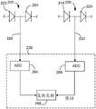
The first light sensor 223 and the second light sensor 224 may be connected as a balanced detector, and the first auxiliary light sensor 218 and the second auxiliary light sensor 220 may also be connected as a balanced detector. For example, fig. 5B provides a schematic illustration of the relationship between the electronic device, the first light sensor 223, the second light sensor 224, the first auxiliary light sensor 218, and the second auxiliary light sensor 220. The symbols of the photodiodes are used to denote the first light sensor 223, the second light sensor 224, the first auxiliary light sensor 218, and the second auxiliary light sensor 220, but one or more of these sensors may have other configurations. In some examples, all of the components shown in the schematic diagram of fig. 5B are included on a LIDAR chip. In some examples, the components shown in the schematic diagram of fig. 5B are distributed between the LIDAR chip and an electronic device located outside of the LIDAR chip.
The electronics couple the first light sensor 223 and the second light sensor 224 as a first balanced detector 225 and the first auxiliary light sensor 218 and the second auxiliary light sensor 220 as a second balanced detector 226. In particular, the first light sensor 223 and the second light sensor 224 are connected in series. Further, the first auxiliary light sensor 218 and the second auxiliary light sensor 220 are connected in series. The series connection in the first balanced detector communicates with a first data line 228, which first data line 228 carries the output from the first balanced detector as a first data signal. The series connection in the second balanced detector is in communication with a second data line 232, the second data line 232 carrying the output from the second balanced detector as a second data signal. The first data signal is an electrical representation of the first composite signal and the second data signal is an electrical representation of the second composite signal. Thus, the first data signal includes contributions from the first waveform and the second waveform, and the second data signal is a composite of the first waveform and the first waveform. The portion of the first waveform in the first data signal is phase shifted relative to the portion of the first waveform in the first data signal, but the portion of the second waveform in the first data signal is in phase relative to the portion of the second waveform in the first data signal. For example, the second data signal includes a portion of the reference signal that is phase shifted relative to a different portion of the reference signal included in the first data signal. Furthermore, the second data signal comprises a comparison signal portion which is in phase with a different portion of the comparison signal comprised in the first data signal. The first and second data signals produce a beat due to the beat between the comparison signal and the reference signal (i.e., the beat in the first and second composite signals).
The electronic device 32 includes a transformation mechanism 238, configured to perform a mathematical transformation on the first data signal and the second data signal. For example, the mathematical transform may be a complex fourier transform with the first data signal and the second data signal as inputs. Since the first data signal is an in-phase component and the second data signal is a quadrature component thereof, the first data signal and the second data signal together act as a complex data signal, wherein the first data signal is a real component of the input and the second data signal is an imaginary component of the input.
The conversion mechanism 238 includes a first analog-to-digital converter (ADC) 264 that receives the first data signal from the first data line 228. The first analog-to-digital converter (ADC) 264 converts the first data signal from an analog form to a digital form and outputs the first digital data signal. The conversion mechanism 238 includes a second analog-to-digital converter (ADC) 266 that receives the second data signal from the second data line 232. The second analog-to-digital converter (ADC) 266 converts the second data signal from an analog form to a digital form and outputs a second digital data signal. The first digital data signal is a digital representation of the first data signal and the second digital data signal is a digital representation of the second data signal. Thus, the first digital data signal and the second digital data signal together are a complex signal, wherein the first digital data signal is a real component of the complex signal and the second digital signal is an imaginary component of the complex signal.
The transformation mechanism 238 includes a transformation component 268 that receives the complex data signal. For example, the conversion component 268 receives as input a first digital data signal from a first analog-to-digital converter (ADC) 264 and also receives a second digital data signal from a second analog-to-digital converter (ADC) 266. The transform component 268 may be configured to perform a mathematical transform on the complex signal to convert from the time domain to the frequency domain. The mathematical transform may be a complex transform, such as a complex Fast Fourier Transform (FFT). Complex transforms such as complex Fast Fourier Transforms (FFTs) provide an unambiguous solution to the frequency offset of the LIDAR input signal relative to the LIDAR output signal, which is caused by the radial velocity between the reflecting object and the LIDAR chip. The electronics further process using the one or more frequency peaks output from the transform component 268 to generate LIDAR data (distance and/or radial velocity between the reflective object and the LIDAR chip or LIDAR system). The transformation component 268 may use firmware, hardware or software, or a combination thereof, to perform the assigned functions.
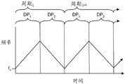
FIG. 5C shows the relationship between system output signal frequency, time, period, and data periodExamples are given. System output signal (f) o ) May be the frequency of the system output signal at the beginning of the cycle.
FIG. 5C shows the notation as period j And period of j+1 Frequency versus time of the sequence of two cycles. In some examples, the frequency versus time pattern repeats in each cycle, as shown in fig. 5C. The illustrated cycles do not include relocation periods and/or relocation periods do not lie between cycles. Thus, fig. 5C illustrates the result of the continuous scan.
Each cycle includes K data periods, each data period being associated with a period index K and labeled DP k . In the example of FIG. 5C, each cycle includes a number labeled DP k Where k =1 and 2. In some examples, the frequency versus time pattern of the data periods corresponding to each other in different cycles is the same, as shown in fig. 5C. The corresponding data periods are data periods having the same period index. Accordingly, each data period DP 1 Can be viewed as corresponding data periods and the associated frequency versus time pattern is the same in fig. 5C. At the end of the cycle, the electronic device returns the frequency to the same frequency level at which the previous cycle was started.
In the data period DP 1 And a data period DP 2 During this time, the electronics operate the light source such that the frequency of the system output signal varies at a linear rate α. Data period DP 1 The direction of the frequency change and the data period DP 2 The direction of the frequency change during this period is reversed.
The frequencies output from the complex fourier transform represent the beat frequencies of composite signals, each of which includes a comparison signal that is beat relative to a reference signal. Beat frequencies (f) from two or more different data periods LDP ) May be combined to generate LIDAR data. For example, according to DP in FIG. 5C 1 The determined beat frequency may be compared with DP according to FIG. 5C 2 The determined beat frequencies are combined to determine LIDAR data. As an example, the following equation applies during a data period during which the electronic device increases the frequency of the outgoing LIDAR signal, such as the data of fig. 5CPeriod DP 1 The method of (1): wherein f is ub Is the frequency provided by the transform component 268 (in this case from DP) 1 Determined f LDP ),f d Indicates the Doppler shift: (
 ) Wherein f is c Represents the optical frequency (f) o ) Where c represents the speed of light, v is the radial velocity between the reflective object and the LIDAR system, where the direction from the reflective object toward the LIDAR system is assumed to be the positive direction, and c is the speed of light. The following equations apply during data periods in which the electronic device reduces the frequency of the outgoing LIDAR signal, such as data period DP of FIG. 5C 2 The method of (1):
 wherein f is db Is the frequency provided by the transform component 268 (in this case from DP) 2 Determined f i,LDP ). In these two equations, f d And τ is unknown. The electronic device solves the two equations for the two unknowns. The radial velocity of the sample region is then quantified based on the Doppler shift (S) ((S))
 ) And/or the sample zones may be spaced apart according to c x f d And/2, quantization.
In some examples, there is more than one object in the sample region. In some instances, when more than one object is present in the sample region, the transform may output more than one frequency, where each frequency is associated with a different object. The frequencies generated by the same object in different data periods of the same cycle can be considered as corresponding frequency pairs. LIDAR data may be generated for each corresponding frequency pair of the transform output. Thus, separate LIDAR data may be generated for each object in the sample region.
Although fig. 5A-5B illustrate multiple optical combining components that combine a portion of the reference signal with a portion of the comparison signal, the processing component may include a single optical combining component that combines the reference signal with the comparison signal to form a composite signal. As a result, at least a portion of the reference signal and at least a portion of the comparison signal may be combined to form a composite signal. The combined portion of the reference signal may be the entire reference signal or a portion of the reference signal, and the combined portion of the comparison signal may be the entire comparison signal or a portion of the comparison signal.
As an example of a processing component that combines a reference signal and a comparison signal to form a composite signal, fig. 5D-5E illustrate the processing component of fig. 5A-5B modified to include a single light combining component. The comparison waveguide 196 carries the comparison signal directly to the first optical combining component 211 and the reference waveguide 198 carries the reference signal directly to the first optical combining component 211.
The first optical combining component 211 combines the comparison signal and the reference signal into a composite signal. The first composite signal produces a beat between the comparison signal and the reference signal due to a frequency difference between the comparison signal and the reference signal. The first light combining component 211 also splits the composite signal onto a first detector waveguide 221 and a second detector waveguide 222. The first detector waveguide 221 carries the first portion of the composite signal to the first photosensor 223, and the first photosensor 223 converts the first portion of the second composite signal to a first electrical signal. The second detector waveguide 222 carries a second portion of the composite signal to a second light sensor 224, and the second light sensor 224 converts the second portion of the second composite signal to a second electrical signal.
Fig. 5E provides a schematic illustration of the relationship between the electronic device, the first light sensor 223 and the second light sensor 224. The symbols of the photodiodes are used to denote the first light sensor 233 and the second light sensor 224, but one or more of these sensors may have other configurations. In some examples, all of the components shown in the schematic diagram of fig. 5E are included on a LIDAR chip. In some examples, the components shown in the schematic diagram of fig. 5E are distributed between the LIDAR chip and an electronic device located outside of the LIDAR chip.
The electronics connect the first light sensor 223 and the second light sensor 224 as a first balanced detector 225. In particular, the first light sensor 233 and the second light sensor 222 are connected in series. The series connection in the first balanced detector communicates with a first data line 228, which first data line 228 carries the output from the first balanced detector as a first data signal. The first data signal is an electrical representation of the composite signal.
The electronics 32 include a transformation mechanism 238 configured to perform a mathematical transformation on the first data signal. The mathematical transform may be a real fourier transform with the first data signal as an input. The electronic device may use the transformed frequency outputs as described above to extract LIDAR data.
Each of the balanced detectors disclosed in the context of fig. 5A to 5E may be replaced by a single light sensor. Thus, the processing component may include one or more light sensors, each of which receives at least a portion of the composite signal, as the received portion of the composite signal may be the entire composite signal or a portion of the composite signal.
As discussed in the context of fig. 5C, electronics 32 tune the frequency of the system output signal. One way to produce such frequency chirps is to modulate the current applied to the light source by the electronics. In semiconductor lasers that can be used as light sources in LIDAR systems, current modulation causes frequency modulation through strong nonlinear carrier/photon coupling.
Fig. 6A and 6B illustrate examples of suitable control assemblies for use as all or a portion of the control assembly 30 disclosed in the context of fig. 1A-1C and 4. The control assembly 30 includes a mach-zehnder interferometer configured to use light from the tapped signal to produce an optical signal having an in-phase component and a quadrature component. The mach-zehnder interferometer receives the tapped signal from the control waveguide 28. The control waveguide directs the tapped signal to a splitter 270, and the splitter 270 splits the tapped signal into a delayed signal and an accelerated signal. The delay waveguide 272 carries the delayed signal to a first splitter 274. The acceleration waveguide 276 carries the acceleration signal to a second splitter 278. The delay waveguide 278 may include a delay section 279, and the delay section 279 may be used to increase the length of the delay waveguide beyond the length of the acceleration waveguide 276. For example, the delay section 279 shown in fig. 6A may represent a spiral arrangement of the delay waveguide 272. Suitable splitters for use as the splitter 270, the first splitter 274 and the second splitter 278 include, but are not limited to, directional couplers, optical couplers, y-junctions, tapered couplers and multi-mode interference (MMI) devices.
The first splitter 274 splits the delayed signal into a first portion of the delayed signal and a second portion of the delayed signal. The first delay waveguide 280 carries a first portion of the delayed signal to a first optical combining component 282. The second delay waveguide 284 carries a second portion of the delayed signal to a second optical combining component 286.
The second splitter 278 splits the acceleration signal into a first portion of the acceleration signal and a second portion of the acceleration signal. The first acceleration waveguide 290 carries a first portion of the acceleration signal to the first optical combining component 282. The second acceleration waveguide 292 carries a second portion of the acceleration signal to the second optical combining component 286.
The second optical combining component 286 combines a second portion of the acceleration signal and a second portion of the delay signal into a second beat signal. As described above, the length of the delay waveguide exceeds the length of the acceleration waveguide 276. Thus, the second portion of the delayed signal is delayed relative to the second portion of the acceleration signal. Because the electronic device may tune the frequency of the outgoing LIDAR signal, the delay causes the second portion of the delayed signal to have a different frequency than the second portion of the accelerated signal. The second beat signal produces a beat between the second portion of the acceleration signal and the second portion of the delay signal due to a frequency difference between the second portion of the acceleration signal and the second portion of the delay signal.
The second optical combining component 286 also separates the second beat signal onto the first auxiliary detector waveguide 294 and the second auxiliary detector waveguide 296. The first auxiliary detector waveguide 294 carries a first portion of the second beat signal to a first auxiliary photosensor 298, and the first auxiliary photosensor 298 converts a second portion of the second beat signal into a first auxiliary electrical signal. The second auxiliary detector waveguide 296 carries a second portion of the second beat signal to the second auxiliary photosensor 300, and the second auxiliary photosensor 300 converts the second portion of the second beat signal to a second auxiliary electrical signal. Examples of suitable photosensors include germanium Photodiodes (PDs) and Avalanche Photodiodes (APDs).
In some examples, the second optical combining component 286 separates the second beat signal such that the portion of the acceleration signal included in the first portion of the second beat signal (i.e., the portion of the second portion of the acceleration signal) is phase shifted 180 relative to the portion of the acceleration signal included in the second portion of the second beat signal (i.e., the portion of the second portion of the acceleration signal) 0 But the portion of the delayed signal in the second portion of the second beat signal (i.e., the portion of the second portion of the delayed signal) is not phase shifted relative to the portion of the delayed signal in the first portion of the second beat signal (i.e., the portion of the second portion of the delayed signal).
The first optical combining component 282 combines a first portion of the acceleration signal and a first portion of the delay signal into a first beat signal. The delay portion 279 delays the first portion of the delayed signal relative to the first portion of the acceleration signal. As a result, the first portion of the delayed signal is delayed relative to the first portion of the acceleration signal. The delay causes the first portion of the delayed signal to have a different frequency than the first portion of the accelerated signal. The first beat signal produces a beat between the second portion of the acceleration signal and the second portion of the delay signal due to a frequency difference between the first portion of the acceleration signal and the first portion of the delay signal.
The first optical combining component 282 also separates the first beat signal onto the first detector waveguide 302 and the second detector waveguide 304. The first detector waveguide 304 carries a first portion of the first beat signal to a first photosensor 306, and the first photosensor 306 converts a first portion of the second beat signal to a first electrical signal. The second detector waveguide 304 carries a second portion of the second beat signal to a second photosensor 308, and the second photosensor 308 converts the second portion of the second beat signal to a second electrical signal. Examples of suitable photosensors include germanium Photodiodes (PDs) and Avalanche Photodiodes (APDs).
In some examples, the first light combining component 282 splits the first beat signal such that the portion of the acceleration signal included in the first portion of the beat signal (i.e., the portion of the first portion of the acceleration signal) is phase shifted 180 relative to the portion of the acceleration signal in the second portion of the beat signal (i.e., the portion of the first portion of the acceleration signal) 0 But the portion of the delayed signal in the first portion of the beat signal (i.e., the portion of the first portion of the delayed signal) is not phase shifted relative to the portion of the delayed signal in the second portion of the beat signal (i.e., the portion of the first portion of the delayed signal).
When the second optical combining component 286 splits the second beat signal such that the portion of the acceleration signal in the first portion of the second beat signal is phase shifted 180 degrees relative to the portion of the acceleration signal in the second portion of the second beat signal 0 The first optical combining component 282 also separates the beat signal such that the portion of the acceleration signal in the first portion of the beat signal is phase shifted 180 relative to the portion of the acceleration signal in the second portion of the beat signal 0 。
The first delay waveguide 280, the second delay waveguide 284, the first acceleration waveguide 290, and the second acceleration waveguide 292 can be configured such that the first beat signal and the second beat signal together are an in-phase component and a quadrature component of the optical process variable signal, wherein the first beat signal is the in-phase component and the second beat signal is the quadrature component of the optical process variable signal, or such that the second beat signal is the in-phase component and the first beat signal is the quadrature component of the optical process variable signal. For example, the first delay waveguide 280 and the second delay waveguide 284 may be configured to provide a phase shift between a first portion of the delayed signal and a second portion of the delayed signal, while the first acceleration waveguide 290 and the second acceleration waveguide 292 are configured such that the first portion of the acceleration signal and the second portion of the acceleration signal are in phase. As an example, the first delay waveguide 280 and the second delay waveguide 284 may be configured to provide a 90 ° phase shift between the first portion of the delayed signal and the second portion of the delayed signal. Thus, one of the delayed signal portions may be a sine function and the other delayed signal portion may be a cosine function operating on the same argument as the sine function. In one example, the first delay waveguide 280 and the second delay waveguide 284 are configured such that a first portion of the delay signal is a cosine function and a second portion of the delay signal is a sine function. In this example, the portion of the delayed signal in the second beat signal is phase shifted relative to the portion of the delayed signal in the first beat signal, however, the portion of the acceleration signal in the first beat signal is not phase shifted relative to the portion of the acceleration signal in the second beat signal.
In another example, the first delay waveguide 280 and the second delay waveguide 284 are configured such that the first portion of the delayed signal and the second portion of the delayed signal are in phase, while the first acceleration waveguide 290 and the second acceleration waveguide 292 are configured to provide a phase shift between the first portion of the acceleration signal and the second portion of the acceleration signal. As an example, the first and second acceleration waveguides 290, 292 may be configured to provide a 90 ° phase shift between a first portion of the acceleration signal and a second portion of the acceleration signal. Thus, one of the acceleration signal portions may be a sine function and the other acceleration signal portion may be a cosine function operating on the same argument as the sine function. In one example, the first and second acceleration waveguides 290, 292 are configured such that a first portion of the acceleration signal is a cosine function and a second portion of the acceleration signal is a sine function operating on the same argument as the cosine function. In this example, the portion of the acceleration signal in the second beat signal is phase shifted relative to the portion of the acceleration signal in the first beat signal, however, the portion of the delayed signal in the first beat signal is not phase shifted relative to the portion of the delayed signal in the second beat signal.
The first light sensor 306 and the second light sensor 308 may be connected as a balanced detector, and the first auxiliary light sensor 298 and the second auxiliary light sensor 300 may also be connected as a balanced detector. For example, FIG. 6B provides a schematic illustration of the relationship between the electronic device, the first light sensor 306, the second light sensor 308, the first auxiliary light sensor 298, and the second auxiliary light sensor 300. The symbols of the photodiodes are used to denote the first light sensor 306, the second light sensor 308, the first auxiliary light sensor 298, and the second auxiliary light sensor 300, but one or more of these sensors may have other configurations. In some examples, all of the components shown in the schematic diagram of fig. 6B are included on a LIDAR chip. In some examples, the components shown in the schematic diagram of fig. 6B are distributed between the LIDAR chip and an electronic device located outside of the LIDAR chip.
The electronics connect the first light sensor 306 and the second light sensor 308 as a first balanced detector 312 and the first auxiliary light sensor 298 and the second auxiliary light sensor 300 as a second balanced detector 314. In particular, the first light sensor 306 and the second light sensor 308 are connected in series. Further, the first auxiliary light sensor 298 and the second auxiliary light sensor 300 are connected in series. The series connection in the first balanced detector communicates with a first data line 316, which first data line 316 carries the output from the first balanced detector as the first process variable signal. The series connection in the second balanced detector communicates with a second data line 318, the second data line 318 carrying the output from the second balanced detector as the first process variable signal.
The first process variable signal is an electrical representation of the first beat signal and the second process variable signal is an electrical representation of the second beat signal. Thus, the first process variable signal produces a beat and the second process variable signal produces a beat. Further, the first process variable signal and the second process variable signal may each carry a different one of the components selected from the group consisting of an in-phase component of the process variable signal and a quadrature component of the process variable signal. For example, the first process variable signal may include contributions from the first and second waveforms, and the second process variable signal may include contributions from the first and second waveforms. The portion of the first waveform in the first process variable signal is phase shifted relative to the portion of the first waveform in the second process variable signal, but the portion of the second waveform in the first process variable signal is in phase relative to the portion of the second waveform in the second process variable signal. For example, the second process variable signal may include a portion of the delayed signal that is phase shifted relative to a different portion of the delayed signal included in the first process variable signal. Further, the second process variable signal may include a portion of the acceleration signal that is in phase with a different portion of the acceleration signal included in the first process variable signal. The first process variable signal and the second process variable signal each produce a beat due to the beat between the acceleration signal and the delay signal (i.e., the beat in the first beat signal and the second beat signal).
The process variable signal is received by the process variable identification component 320. The process variable identification component 320 uses the process variable signal to output an indicator signal that indicates the frequency (f) of the tapped signal TS ) Is the frequency (f) of the tapped signal TS ) And/or can be used to determine the frequency (f) of the tapped signal TS ). In some examples, the indicator signal is of a frequency (f) that is the same as the tapped signal TS ) An analog signal of the associated one or more characteristics. In some examples, the indicator signal is a digital signal that quantifies the frequency (f) of the tapped signal TS ) With the frequency (f) of the tapped signal TS ) Correlation, or may be used to quantify the frequency (f) of the tapped signal TS ). Since the system output signal and the tapped signal represent portions of the outgoing LIDAR signal, the frequency (f) of the tapped signal TS ) May represent frequency values of the outgoing LIDAR signals and/or system output signals.
The indicator signal may be received by the light control component 322. The light control component 332 may control the light source in response to the indicator signal. For example, the light source may be controlled in a control architecture, wherein the frequency (f) of the signal is tapped TS ) Used as a control process variable. When the process variable is the frequency of the tapped signal, the expected frequency of the LIDAR output signal is used as a reference variable. Because the frequency of the LIDAR output signal is modulated, the desired frequency of the LIDAR input signal represented by the tap signal varies as a function of time. For triangular modulation, fig. 5C may represent an example of a desired waveform. Such asAs is clear from fig. 5C, the frequency of the tapped signal is a linear function of time. Thus, the control mechanism may control the light source such that the frequency of the tapped signal substantially maintains a desired waveform. Suitable control mechanisms include, but are not limited to, control architectures that utilize feedback control and/or feedforward control. Thus, the control mechanism may be a feedback control loop.
The light control component 322 can control a characteristic of the tapped signal, and accordingly the outgoing LIDAR signal and/or the system output signal, in response to a value of the error signal determined by the value of the controlled process variable at a particular point in time and the value of the reference variable at the same point in time. For example, the optical control component 322 may control the characteristics of the tapped signal in order to reduce the value of the error signal. As an example, the light control component 322 may control a characteristic of the tap signal such that the value of the control process variable is moved toward the value of the reference variable. In some examples, the control mechanism is a control loop, such as a feedback control loop. When the control mechanism is a feedback control loop, the error signal of the control mechanism may be equal to the difference between the value of the control process variable and the value of the reference variable at a particular point in time.
When the process variable is the frequency of the tapped signal, the optical control component 322 may transmit an optical control signal that tunes the frequency of the tapped signal. For example, the optical control component 322 can tune the frequency of the tap signal by transmitting an optical control signal that changes the current level through the light source. Other light control signals are possible. For example, when the light source is an electrostatic MEMS tunable laser, the optical control component 322 can tune the frequency of the tapped signal by transmitting an optical control signal that changes the voltage level of the MEMS facet that moves the MEMS tunable laser.
In some examples, the light control component 322 and/or the process variable identification component 320 actually quantizes the tapped signal (f) TS ) (ii) a However, such quantification is not necessary. For example, when the indicator signal is an include-and-drop signal (f) TS ) With an analog signal of related characteristics, the optical control signal can be derived directly from the indicator signal without actually quantizing the frequency (f) of the tapped signal TS ). For example, the control signal may be an indicator signalSign and/or a one-to-one function of the transformed signal discussed below. As an example, the control signal may be a one-to-one function of the instantaneous frequency.
Fig. 6C illustrates on the same time axis the amplitude of the in-phase and quadrature components of the optical process variable signal and/or the process variable signal versus the frequency of the system output signal. For example, fig. 6C can compare the frequency of the system output signal during the first two data periods shown in fig. 5C with the changes in the in-phase and quadrature components of the optical process variable signal and/or the process variable signal. Although fig. 6C illustrates the optical process variable signal and/or the process variable signal having only one period per data period, the optical process variable signal and/or the process variable signal may have more than one period per data period.
Various process variable identification components 320 can be used to determine the value of a process variable indicator. Fig. 6D illustrates one example of a process variable identification component 320 that is suitable for use when the process variable is a frequency of a tapped signal, an outgoing LIDAR signal, and/or a system output signal. The illustrated process variable identification component 320 includes a local oscillator 324 that outputs a local signal including a first local signal and a second local signal. The first local signal and the second local signal each carry a different one of components selected from the group consisting of an in-phase component of the local signal and a quadrature component of the local signal.
The process variable identification component 320 also includes a first multiplier 326 that receives the first process variable signal and the first local signal. The first multiplier 326 multiplies the first process variable signal with the first local signal. The first local signal carries a quadrature component of the local signal when the first process variable signal carries an in-phase component of the process variable signal. The first local signal carries an in-phase component of the local signal when the first process variable signal carries a quadrature component of the process variable signal. The first multiplier 326 outputs a first multiplied signal.
The process variable identification component 320 also includes a second multiplier 328 that receives a second process variable signal and a second local signal. A second multiplier 328 multiplies the second process variable signal with a second local signal. The second local signal carries a quadrature component of the local signal when the second process variable signal carries an in-phase component of the process variable signal. The second local signal carries an in-phase component of the local signal when the second process variable signal carries a quadrature component of the process variable signal. The second multiplier 326 outputs a second multiplied signal.
The process variable identification component 320 includes an adder 330 that receives the first multiplied signal and the second multiplied signal. The adder 330 adds the first multiplied signal and the second multiplied signal and outputs a control signal.
The control signal is received at the process variable estimator 334. The process variable estimator 334 uses the control signal to output a signal having a frequency (f) equal to the tapped signal TS ) An indicator signal of the associated one or more characteristics. For example, the process variable estimator 334 may be a time To Digital Converter (TDC) with an output having a frequency (f) that is equal to the tapped signal TS ) An indicator signal of the associated voltage. In some examples, a time-to-digital converter (TDC) output voltage is related to the frequency (f) of the tapped signal TS ) A proportional indicator signal. The indicator signal may be received by the light control component 322 for controlling the frequency of the light source.
Another example of a suitable process variable estimator 334 is a frequency counter that outputs an indicator signal indicating the time between baseline crossings (dn) of the control signal. Frequency (f) determined for tapped signals TS ) The time correlation between the baseline crossing (dn) can be determined by equation 1: f. of TS =f LO -1/(2 × dn), wherein f LO Representing the frequency of the local oscillator. The process variable estimator 334 may output an indicator signal carrying an indication of the frequency (f) determined for the tapped signal TS ) Data of values of (a). The indicator signal may be received by the light control component 322 for controlling the frequency of the light source.
The local signal is selected such that the frequency of the control signal is higher than the frequency of the process variable signal. The increased frequency of the control signal increases the frequency at which the process variable can be accurately sampled. Increasing the sampling frequency provides a more accurate control of the process variable by the control mechanism. As a result, the increased frequency of the control signal enhances the control of the process variable by the control mechanism. Suitable sampling frequencies include, but are not limited to, sampling frequencies that are 100 times the modulation frequency, where the modulation frequency is 1/(cycle duration). In some examples, all or a portion of the data periods in each cycle have a sampling frequency that exceeds 30 or 100 times the duration of each data period. In some examples, the local signal is selected such that the frequency of the control signal is more than 100 times and less than 10000 times the frequency of the process variable signal.
Fig. 6E illustrates another example of a suitable process variable identification component 320 that is suitable for use when the process variable is a frequency of a tapped signal, an outgoing LIDAR signal, and/or a system output signal. The process variable identification component 320 includes an analog-to-digital converter (ADC) 340 that receives a control signal from the summer 330. An analog-to-digital converter (ADC) 340 converts the first process variable signal from an analog form to a digital form and outputs a digital data signal. The digital data signal is a digital representation of the control signal.
The process variable identification component 320 includes a transformation component 342 that receives a digital data signal. The transform component 342 performs a mathematical transform on the digital data signal. The mathematical transform is selected such that the transform component 342 outputs a transform signal that is related to, includes, or is indicative of the frequency of the LIDAR output signal. Suitable first mathematical transforms include, but are not limited to, the hilbert transform. The hilbert transform outputs a transform signal indicative of the instantaneous phase of the control signal and hence of the frequency of the control signal.
The transformed signal is received by a frequency estimator 344. The frequency estimator may be configured to output an indicator signal related to, including, and/or indicative of a frequency of the LIDAR output signal. For example, the frequency estimator may pass f TS =(finst- f LO ) (T/tau) converting the instantaneous frequency into the frequency (f) of the tapped signal TS ) Wherein f is LO Is the frequency of the local oscillator, finst is the instantaneous frequency extracted from the Hilbert transform, T is the duration of the data period in the triangular modulation scheme, and τ is caused by the difference in length between the delay and acceleration waveguides 272 and 276The delay of (2). Thus, the indicator signal may be the frequency (f) of the quantized tapped signal TS ) The digital signal of (2). The indicator signal may be received by the light control component 322 for controlling the frequency of the light source.
Although the indicator signal is described in the context of a signal carrying data about the frequency of the tapped signal, the indicator signal may carry data that is indirectly related to the frequency of the tapped signal. For example, the indicator signal may carry data that may be used to determine the frequency of the tapped signal. As an example, the frequency (f) of the tapped signal TS ) May be determined based on the rate of change of the phase of the tapped signal. Thus, the indicator signal may carry data indicative of the rate of change of the phase of the tapped signal.
The process variable identification component 320 reduces the amount of delay that needs to be generated by the delay waveguide 272 because it increases the sensitivity of the indicator signal to the frequency of the tapped signal by combining information from the in-phase and quadrature components at any given time. Existing systems attempt to increase this sensitivity by increasing the length of the delay waveguide 272. Because the process variable identification component 320 increases the sensitivity of the indicator signal, the length of the delay waveguide 276 can exceed the length of the acceleration waveguide 276 by a smaller amount than is possible in prior systems. For example, the time delay in the delay waveguide 272 may exceed the time delay in the acceleration waveguide 276 by an amount greater than or equal to 50ps and less than or equal to 100 ns. In one example, the length of the delay waveguide 272 exceeds the length of the acceleration waveguide 276 by an amount less than 1000cm, less than 500cm, or less than 100cm, and greater than 0.0cm or 0.4 cm. In one example, the delay waveguide 272 and the acceleration waveguide 276 guide light through silicon, and the length of the delay waveguide 276 exceeds the length of the acceleration waveguide 272 by an amount less than 1000cm and greater than 0.0cm or 0.4 cm.
Suitable platforms for LIDAR chips include, but are not limited to, silicon dioxide, indium phosphide, and silicon-on-insulator wafers. Fig. 7 is a cross-section of a chip portion constructed from a silicon-on-insulator wafer. A silicon-on-insulator (SOI) wafer includes a buried layer 310 between a substrate 312 and an optical transmission medium 314. In a silicon-on-insulator wafer, the buried layer 310 is silicon dioxide, while the substrate 312 and the optical transmission medium 314 are silicon. The substrate 312 of the optical platform, such as an SOI wafer, may serve as a base for the entire LIDAR chip. For example, the optical components shown on the LIDAR chips of fig. 1A-1C may be positioned on or above the top and/or lateral sides of the substrate 312.
Fig. 7 is a cross-section of a portion of a LIDAR chip including a waveguide configuration suitable for use with a LIDAR chip constructed from a silicon-on-insulator wafer. The ridge 316 of the light-transmitting medium extends away from a slab region 318 in the light-transmitting medium. The optical signal is confined between the top of the ridge 316 and the buried oxide layer 310.
The dimensions of the ridge waveguide are marked in fig. 7. For example, the ridge has a width denoted w and a height denoted h. The thickness of the slab region is denoted T. For LIDAR applications, these dimensions may be more important than others because of the need to use higher levels of optical power than used in other applications. The ridge width (denoted w) is greater than 1 μm and less than 4 μm, the ridge height (denoted h) is greater than 1 μm and less than 4 μm, the slab region thickness is greater than 0.5 μm and less than 3 μm, these dimensions may apply to straight or substantially straight portions of the waveguide, curved portions of the waveguide, and tapered portions of the waveguide(s). Thus, these portions of the waveguide will be single mode. However, in some instances, these dimensions apply to straight or substantially straight portions of the waveguide. Additionally or alternatively, the curved portion of the waveguide may have a reduced slab thickness in order to reduce optical losses in the curved portion of the waveguide. For example, the curved portion of the waveguide may have a ridge extending away from a slab region having a thickness greater than or equal to 0.0 μm and less than 0.5 μm. While the above dimensions will generally provide straight or substantially straight portions of the waveguide having a single mode configuration, they may produce multi-mode tapered section(s) and/or curved section(s). Coupling between multi-mode geometry and single-mode geometry may be accomplished using a taper that does not substantially excite higher order modes. Thus, the waveguide may be configured such that signals carried in the waveguide are carried in a single mode even when carried in a waveguide section having a multi-mode size. The waveguide configuration disclosed in the context of fig. 7 is suitable for all or part of the waveguides on a LIDAR chip constructed in accordance with fig. 1A-1C.
The light sensor that interfaces with the waveguide on the LIDAR chip may be a component that is separate from the chip and then attached to the chip. For example, the light sensor may be a photodiode or an avalanche photodiode. Examples of suitable light sensor components include, but are not limited to, inGaAs PIN photodiodes manufactured by hamamatsu located in hamamatsu, japan, or InGaAs APDs (avalanche photodiodes) manufactured by hamamatsu located in hamamatsu, japan. These light sensors may be located in the center of the LIDAR chip. Alternatively, all or a portion of the waveguide terminating in the light sensor may terminate in a facet at the edge of the chip, and the light sensor may be attached to the edge of the chip above the facet such that the light sensor receives light through the facet. The use of the light sensor as a component separate from the chip is suitable for all or part of the light sensor selected from the group consisting of the first auxiliary light sensor 218, the second auxiliary light sensor 220, the first light sensor 223, and the second light sensor 224.
Instead of the light sensor as a separate component, all or part of the light sensor may be integrated with the chip. Examples of optical sensors that interface with ridge waveguides on a chip constructed from a silicon-on-insulator wafer can be found in the following documents, for example: optics Express Vol. 15, no. 21, 13965-13971 (2007); U.S. patent No. 8,093,080 issued on month 10 of 2012; U.S. patent No. 8,242,432 issued on 8/14/2012; and us patent No. 6,108,8472 issued on 8/22/2000, each of which is incorporated herein in its entirety. The use of a chip-integrated light sensor is suitable for all or part of the light sensors selected from the group consisting of the secondary light sensor 218, the second secondary light sensor 220, the first light sensor 223 and the second light sensor 224.
The light source 4 interfacing with the utility waveguide 12 may be a laser chip that is separate from and then attached to the LIDAR chip. For example, the light source 4 may be a laser chip attached to the chip using a flip-chip arrangement. When the light source 4 is to be interfaced with a ridge waveguide on a chip constructed from a silicon-on-insulator wafer, it is appropriate to use a flip-chip arrangement. Alternatively, the utility waveguide 12 may include an optical grating (not shown), such as a bragg grating, which acts as a reflector for the external cavity laser. In these examples, the light source 4 may include a gain element that is separate from the LIDAR chip and then attached to the LIDAR chip in a flip-chip arrangement. Examples of suitable interfaces between flip-chip gain elements constructed from silicon-on-insulator wafers and ridge waveguides can be found in us patent No. 9,705,278, published 2017, month 11 and us patent No. 5,991,484, published 1999, month 11, 23; each of which is incorporated herein in its entirety. When the light source 4 is a gain element or laser chip, the electronics 32 can change the frequency of the outgoing LIDAR signal by changing the level of current applied through the gain element or laser cavity.
The above-described LIDAR system includes a plurality of optical components, such as a LIDAR chip, a LIDAR adapter, a light source, a light sensor, a waveguide, and an amplifier. In some examples, the LIDAR system includes one or more passive optical components in addition to or instead of the optical components shown. The passive optical component may be a solid state component that excludes moving parts. Suitable passive optical components include, but are not limited to, lenses, mirrors, optical gratings, reflective surfaces, splitters, demultiplexers, multiplexers, polarizers, polarization splitters, and polarization rotators. In some instances, the LIDAR system includes one or more active optical components in addition to, or instead of, the optical components shown. Suitable active optical components include, but are not limited to, optical switches, phase tuners, attenuators, steerable mirrors, steerable lenses, tunable demultiplexers, tunable multiplexers.
Other embodiments, combinations, and modifications of the invention will readily occur to those of ordinary skill in the art in view of these teachings. Accordingly, the invention is not to be restricted except in light of the attached claims, which include all such embodiments and modifications when viewed in conjunction with the above specification and accompanying drawings.
Claims (18)
1. A LIDAR system, comprising:
at least one optical component configured to output a system output signal that travels away from the LIDAR system and is capable of being reflected by an object located outside the LIDAR system; and
a control mechanism configured to control one or more process variables of the system output signal, the control mechanism controlling the process variable using an electrical process variable signal, the process variable signal comprising an in-phase component and a quadrature component.
2. The system of claim 1, wherein the control mechanism is a control loop.
3. The system of claim 2, wherein the control loop is a feedback control loop.
4. The system of claim 1, wherein the control mechanism is configured to multiply the process variable signal by a local signal comprising an in-phase component and a quadrature component.
5. The system of claim 1, wherein the system output signal and the tap signal each comprise light from the outgoing LIDAR signal, and the control mechanism uses the tap signal to determine a value of a process variable of the system output signal.
6. The system of claim 5, wherein the control mechanism comprises a Mach-Zehnder interferometer that receives the tapped signal and is configured to generate an optical signal from the tapped signal, the optical signal having an in-phase component and a quadrature component.
7. The system of claim 6, wherein the Mach-Zehnder interferometer is configured to split light from the tapped signal onto a delay waveguide and an acceleration waveguide, the length of the delay waveguide being less than 100cm longer than the length of the acceleration waveguide.
8. The system of claim 1, wherein the control mechanism comprises a mach-zehnder interferometer configured to generate an optical signal having an in-phase component and a quadrature component.
9. The system of claim 8, wherein the optical signal produces beats.
10. The system of claim 8, wherein the mach-zehnder interferometer is included on a LIDAR chip.
11. The system of claim 8, wherein the LIDAR chip is constructed on a silicon-on-insulator platform.
12. The system of claim 11, wherein the system output signal and the tapped signal each comprise light from the outgoing LIDAR signal, and the control mechanism uses the tapped signal to determine a value of a process variable of the system output signal, and
the system output signal, the tap signal, and the outgoing LIDAR signal are each guided by different waveguides on the LIDAR chip.
13. The system of claim 6, wherein the control mechanism is configured to convert the optical signal to an electrical process variable signal.
14. The system of claim 1 wherein the process variable is a frequency of the system output signal.
15. The system of claim 14, wherein the frequency of the system output signal varies over a repeating cycle, and the value of the frequency of the system output signal is determined at a frequency exceeding 100 times per cycle duration.
16. The system of claim 1, wherein the frequency of the system output signal varies at a non-zero rate for the duration of the data period, and the value of the frequency of the system output signal is determined more than 100 times during the duration of the data period.
17. The system of claim 1 wherein the process variable is a phase of a system output signal.
18. A method, comprising:
causing a LIDAR system to output a system output signal that travels away from the LIDAR system and is capable of being reflected by an object located outside of the LIDAR system; and
one or more process variables of the system output signal are controlled in a control mechanism that uses an electrical process variable signal to control the process variable, the process variable signal including an in-phase component and a quadrature component.
Applications Claiming Priority (3)
| Application Number | Priority Date | Filing Date | Title |
|---|---|---|---|
| US16/875,987 US20210356592A1 (en) | 2020-05-16 | 2020-05-16 | Monitoring signal chirp in lidar output signals |
| US16/875987 | 2020-05-16 | ||
| PCT/US2021/032095 WO2021236399A1 (en) | 2020-05-16 | 2021-05-12 | Monitoring signal chirp in lidar output signals |
Publications (1)
| Publication Number | Publication Date |
|---|---|
| CN115485580A true CN115485580A (en) | 2022-12-16 |
Family
ID=78513241
Family Applications (1)
| Application Number | Title | Priority Date | Filing Date |
|---|---|---|---|
| CN202180035663.5A Pending CN115485580A (en) | 2020-05-16 | 2021-05-12 | Monitoring signal chirp in LIDAR output signals |
Country Status (5)
| Country | Link |
|---|---|
| US (1) | US20210356592A1 (en) |
| EP (1) | EP4150376A1 (en) |
| JP (1) | JP2023529564A (en) |
| CN (1) | CN115485580A (en) |
| WO (1) | WO2021236399A1 (en) |
Families Citing this family (2)
| Publication number | Priority date | Publication date | Assignee | Title |
|---|---|---|---|---|
| US11698448B1 (en) * | 2020-06-25 | 2023-07-11 | Silc Technologies, Inc. | Reduction of electrical components in LIDAR systems for identifying a beat frequency by using peaks of outputs of two transforms |
| EP4330718A1 (en) * | 2021-04-29 | 2024-03-06 | SiLC Technologies, Inc. | Reducing size of lidar system control assemblies |
Family Cites Families (10)
| Publication number | Priority date | Publication date | Assignee | Title |
|---|---|---|---|---|
| JPH1065697A (en) * | 1996-08-23 | 1998-03-06 | Oki Electric Ind Co Ltd | Band management circuit |
| US6389000B1 (en) * | 1997-09-16 | 2002-05-14 | Qualcomm Incorporated | Method and apparatus for transmitting and receiving high speed data in a CDMA communication system using multiple carriers |
| JP2004093787A (en) * | 2002-08-30 | 2004-03-25 | Seiko Epson Corp | Optical switch, device for optical communication and optical communication system |
| US9683928B2 (en) * | 2013-06-23 | 2017-06-20 | Eric Swanson | Integrated optical system and components utilizing tunable optical sources and coherent detection and phased array for imaging, ranging, sensing, communications and other applications |
| AU2014284466A1 (en) * | 2013-07-03 | 2015-12-24 | California Institute Of Technology | High-coherence semiconductor light sources |
| JP7140784B2 (en) * | 2017-03-01 | 2022-09-21 | ポイントクラウド インコーポレイテッド | Modular 3D optical detection system |
| US10401495B2 (en) * | 2017-07-10 | 2019-09-03 | Blackmore Sensors and Analytics Inc. | Method and system for time separated quadrature detection of doppler effects in optical range measurements |
| US10613200B2 (en) * | 2017-09-19 | 2020-04-07 | Veoneer, Inc. | Scanning lidar system and method |
| US11378691B2 (en) * | 2018-05-15 | 2022-07-05 | Silc Technologies, Inc. | Generation of LIDAR data from optical signals |
| WO2021150826A1 (en) * | 2020-01-23 | 2021-07-29 | Ours Technology Inc. | On-chip monitoring and calibration circuits for frequency modulated continous wave lidar |
-
2020
- 2020-05-16 US US16/875,987 patent/US20210356592A1/en active Pending
-
2021
- 2021-05-12 JP JP2022568583A patent/JP2023529564A/en active Pending
- 2021-05-12 EP EP21807500.0A patent/EP4150376A1/en active Pending
- 2021-05-12 WO PCT/US2021/032095 patent/WO2021236399A1/en active Application Filing
- 2021-05-12 CN CN202180035663.5A patent/CN115485580A/en active Pending
Also Published As
| Publication number | Publication date |
|---|---|
| JP2023529564A (en) | 2023-07-11 |
| US20210356592A1 (en) | 2021-11-18 |
| WO2021236399A1 (en) | 2021-11-25 |
| EP4150376A1 (en) | 2023-03-22 |
Similar Documents
| Publication | Publication Date | Title |
|---|---|---|
| US11782134B2 (en) | Optical manifold for lidar applications | |
| US11892565B2 (en) | Controlling direction of LIDAR output signals | |
| US11714194B2 (en) | Reduction of sampling rates in lidar systems | |
| CN113544532A (en) | Amplification of LIDAR output signals | |
| CN115485580A (en) | Monitoring signal chirp in LIDAR output signals | |
| US20210239811A1 (en) | Increasing power of signals output from lidar systems | |
| US11624826B2 (en) | Use of common chirp periods in generation of LIDAR data | |
| US20220291361A1 (en) | Use of circulator in lidar system | |
| US11982743B2 (en) | Reducing size of LIDAR system control assemblies | |
| US20220350023A1 (en) | Reducing size of lidar system control assemblies | |
| US20220404470A1 (en) | Scanning multiple lidar system output signals | |
| US20230288567A1 (en) | Imaging system having reduced adc sampling rates | |
| US20210349197A1 (en) | Reducing amplitude variations in lidar system output signals | |
| US20240134018A1 (en) | Identification of chirp rates | |
| US20220317252A1 (en) | Adjusting lidar data in response to edge effects | |
| US20230258786A1 (en) | Data refinement in optical systems | |
| US20220113390A1 (en) | Increasing signal-to-noise ratios in lidar systems | |
| US20240085559A1 (en) | Combining data from different sample regions in an imaging system field of view | |
| US20230069201A1 (en) | Use of multiple steering mechanisms in scanning | |
| WO2024086014A1 (en) | Identification of chirp rates |
Legal Events
| Date | Code | Title | Description |
|---|---|---|---|
| PB01 | Publication | ||
| PB01 | Publication | ||
| SE01 | Entry into force of request for substantive examination | ||
| SE01 | Entry into force of request for substantive examination |