CN115427184A - Machining system and measuring member - Google Patents
Machining system and measuring member Download PDFInfo
- Publication number
- CN115427184A CN115427184A CN202080099822.3A CN202080099822A CN115427184A CN 115427184 A CN115427184 A CN 115427184A CN 202080099822 A CN202080099822 A CN 202080099822A CN 115427184 A CN115427184 A CN 115427184A
- Authority
- CN
- China
- Prior art keywords
- light
- light receiving
- processing
- machining
- energy beam
- Prior art date
- Legal status (The legal status is an assumption and is not a legal conclusion. Google has not performed a legal analysis and makes no representation as to the accuracy of the status listed.)
- Pending
Links
- 238000003754 machining Methods 0.000 title claims description 480
- 238000012545 processing Methods 0.000 claims abstract description 793
- 238000005259 measurement Methods 0.000 claims description 169
- 230000003287 optical effect Effects 0.000 claims description 116
- 238000000034 method Methods 0.000 claims description 69
- 230000008569 process Effects 0.000 claims description 44
- 239000003550 marker Substances 0.000 claims description 38
- 230000008859 change Effects 0.000 claims description 31
- 239000000126 substance Substances 0.000 claims description 16
- 239000004973 liquid crystal related substance Substances 0.000 claims 1
- 230000001678 irradiating effect Effects 0.000 abstract description 10
- 210000003128 head Anatomy 0.000 description 130
- 239000000463 material Substances 0.000 description 68
- 238000003384 imaging method Methods 0.000 description 60
- 230000006870 function Effects 0.000 description 35
- 239000007789 gas Substances 0.000 description 27
- 230000002093 peripheral effect Effects 0.000 description 23
- 238000001514 detection method Methods 0.000 description 19
- 239000000470 constituent Substances 0.000 description 17
- 210000001747 pupil Anatomy 0.000 description 14
- 238000004590 computer program Methods 0.000 description 13
- 238000010586 diagram Methods 0.000 description 12
- 238000009826 distribution Methods 0.000 description 11
- 238000005286 illumination Methods 0.000 description 10
- 239000011295 pitch Substances 0.000 description 10
- 230000005540 biological transmission Effects 0.000 description 9
- 238000007493 shaping process Methods 0.000 description 9
- 238000006073 displacement reaction Methods 0.000 description 8
- 230000000694 effects Effects 0.000 description 8
- 230000009471 action Effects 0.000 description 6
- 230000010355 oscillation Effects 0.000 description 6
- 239000011521 glass Substances 0.000 description 5
- 239000004065 semiconductor Substances 0.000 description 5
- 238000013461 design Methods 0.000 description 4
- 239000012530 fluid Substances 0.000 description 4
- 238000003860 storage Methods 0.000 description 4
- 239000000758 substrate Substances 0.000 description 4
- 238000013459 approach Methods 0.000 description 3
- 230000002238 attenuated effect Effects 0.000 description 3
- 238000005520 cutting process Methods 0.000 description 3
- 230000004048 modification Effects 0.000 description 3
- 238000012986 modification Methods 0.000 description 3
- 239000012778 molding material Substances 0.000 description 3
- 240000002853 Nelumbo nucifera Species 0.000 description 2
- 235000006508 Nelumbo nucifera Nutrition 0.000 description 2
- 235000006510 Nelumbo pentapetala Nutrition 0.000 description 2
- 238000002679 ablation Methods 0.000 description 2
- JNDMLEXHDPKVFC-UHFFFAOYSA-N aluminum;oxygen(2-);yttrium(3+) Chemical compound [O-2].[O-2].[O-2].[Al+3].[Y+3] JNDMLEXHDPKVFC-UHFFFAOYSA-N 0.000 description 2
- 239000004918 carbon fiber reinforced polymer Substances 0.000 description 2
- 238000006243 chemical reaction Methods 0.000 description 2
- 238000004891 communication Methods 0.000 description 2
- 239000007788 liquid Substances 0.000 description 2
- 239000000155 melt Substances 0.000 description 2
- 239000007769 metal material Substances 0.000 description 2
- 238000001465 metallisation Methods 0.000 description 2
- 239000002245 particle Substances 0.000 description 2
- 239000000843 powder Substances 0.000 description 2
- 230000009467 reduction Effects 0.000 description 2
- 239000011347 resin Substances 0.000 description 2
- 229920005989 resin Polymers 0.000 description 2
- 229910019901 yttrium aluminum garnet Inorganic materials 0.000 description 2
- 241000251730 Chondrichthyes Species 0.000 description 1
- VYZAMTAEIAYCRO-UHFFFAOYSA-N Chromium Chemical compound [Cr] VYZAMTAEIAYCRO-UHFFFAOYSA-N 0.000 description 1
- 229910000737 Duralumin Inorganic materials 0.000 description 1
- WGLPBDUCMAPZCE-UHFFFAOYSA-N Trioxochromium Chemical compound O=[Cr](=O)=O WGLPBDUCMAPZCE-UHFFFAOYSA-N 0.000 description 1
- 239000000853 adhesive Substances 0.000 description 1
- 230000001070 adhesive effect Effects 0.000 description 1
- 229910045601 alloy Inorganic materials 0.000 description 1
- 239000000956 alloy Substances 0.000 description 1
- 230000004075 alteration Effects 0.000 description 1
- 230000003373 anti-fouling effect Effects 0.000 description 1
- 201000009310 astigmatism Diseases 0.000 description 1
- 230000000903 blocking effect Effects 0.000 description 1
- 238000004364 calculation method Methods 0.000 description 1
- 239000000919 ceramic Substances 0.000 description 1
- 229910052804 chromium Inorganic materials 0.000 description 1
- 239000011651 chromium Substances 0.000 description 1
- 229910000423 chromium oxide Inorganic materials 0.000 description 1
- 238000004140 cleaning Methods 0.000 description 1
- 239000002131 composite material Substances 0.000 description 1
- 238000000151 deposition Methods 0.000 description 1
- 230000008021 deposition Effects 0.000 description 1
- 238000010894 electron beam technology Methods 0.000 description 1
- 239000000835 fiber Substances 0.000 description 1
- RFHAOTPXVQNOHP-UHFFFAOYSA-N fluconazole Chemical compound C1=NC=NN1CC(C=1C(=CC(F)=CC=1)F)(O)CN1C=NC=N1 RFHAOTPXVQNOHP-UHFFFAOYSA-N 0.000 description 1
- 239000003517 fume Substances 0.000 description 1
- 239000008187 granular material Substances 0.000 description 1
- 238000000227 grinding Methods 0.000 description 1
- 238000009499 grossing Methods 0.000 description 1
- 238000005305 interferometry Methods 0.000 description 1
- 238000010884 ion-beam technique Methods 0.000 description 1
- 238000012538 light obscuration Methods 0.000 description 1
- 230000007246 mechanism Effects 0.000 description 1
- 229910052751 metal Inorganic materials 0.000 description 1
- 239000002184 metal Substances 0.000 description 1
- 239000012768 molten material Substances 0.000 description 1
- 230000000149 penetrating effect Effects 0.000 description 1
- 238000005498 polishing Methods 0.000 description 1
- 239000012260 resinous material Substances 0.000 description 1
- 229910052710 silicon Inorganic materials 0.000 description 1
- 239000010703 silicon Substances 0.000 description 1
- 239000000779 smoke Substances 0.000 description 1
- 239000007921 spray Substances 0.000 description 1
- 230000001360 synchronised effect Effects 0.000 description 1
- 238000002834 transmittance Methods 0.000 description 1
Images


Classifications
-
- B—PERFORMING OPERATIONS; TRANSPORTING
- B23—MACHINE TOOLS; METAL-WORKING NOT OTHERWISE PROVIDED FOR
- B23K—SOLDERING OR UNSOLDERING; WELDING; CLADDING OR PLATING BY SOLDERING OR WELDING; CUTTING BY APPLYING HEAT LOCALLY, e.g. FLAME CUTTING; WORKING BY LASER BEAM
- B23K26/00—Working by laser beam, e.g. welding, cutting or boring
- B23K26/70—Auxiliary operations or equipment
- B23K26/702—Auxiliary equipment
- B23K26/705—Beam measuring device
-
- B—PERFORMING OPERATIONS; TRANSPORTING
- B23—MACHINE TOOLS; METAL-WORKING NOT OTHERWISE PROVIDED FOR
- B23K—SOLDERING OR UNSOLDERING; WELDING; CLADDING OR PLATING BY SOLDERING OR WELDING; CUTTING BY APPLYING HEAT LOCALLY, e.g. FLAME CUTTING; WORKING BY LASER BEAM
- B23K26/00—Working by laser beam, e.g. welding, cutting or boring
- B23K26/08—Devices involving relative movement between laser beam and workpiece
- B23K26/083—Devices involving movement of the workpiece in at least one axial direction
-
- B—PERFORMING OPERATIONS; TRANSPORTING
- B23—MACHINE TOOLS; METAL-WORKING NOT OTHERWISE PROVIDED FOR
- B23K—SOLDERING OR UNSOLDERING; WELDING; CLADDING OR PLATING BY SOLDERING OR WELDING; CUTTING BY APPLYING HEAT LOCALLY, e.g. FLAME CUTTING; WORKING BY LASER BEAM
- B23K26/00—Working by laser beam, e.g. welding, cutting or boring
- B23K26/02—Positioning or observing the workpiece, e.g. with respect to the point of impact; Aligning, aiming or focusing the laser beam
- B23K26/03—Observing, e.g. monitoring, the workpiece
- B23K26/032—Observing, e.g. monitoring, the workpiece using optical means
-
- B—PERFORMING OPERATIONS; TRANSPORTING
- B23—MACHINE TOOLS; METAL-WORKING NOT OTHERWISE PROVIDED FOR
- B23K—SOLDERING OR UNSOLDERING; WELDING; CLADDING OR PLATING BY SOLDERING OR WELDING; CUTTING BY APPLYING HEAT LOCALLY, e.g. FLAME CUTTING; WORKING BY LASER BEAM
- B23K26/00—Working by laser beam, e.g. welding, cutting or boring
- B23K26/14—Working by laser beam, e.g. welding, cutting or boring using a fluid stream, e.g. a jet of gas, in conjunction with the laser beam; Nozzles therefor
- B23K26/142—Working by laser beam, e.g. welding, cutting or boring using a fluid stream, e.g. a jet of gas, in conjunction with the laser beam; Nozzles therefor for the removal of by-products
-
- B—PERFORMING OPERATIONS; TRANSPORTING
- B23—MACHINE TOOLS; METAL-WORKING NOT OTHERWISE PROVIDED FOR
- B23K—SOLDERING OR UNSOLDERING; WELDING; CLADDING OR PLATING BY SOLDERING OR WELDING; CUTTING BY APPLYING HEAT LOCALLY, e.g. FLAME CUTTING; WORKING BY LASER BEAM
- B23K26/00—Working by laser beam, e.g. welding, cutting or boring
- B23K26/36—Removing material
Landscapes
- Engineering & Computer Science (AREA)
- Physics & Mathematics (AREA)
- Optics & Photonics (AREA)
- Plasma & Fusion (AREA)
- Mechanical Engineering (AREA)
- Laser Beam Processing (AREA)
Abstract
A processing system for processing an object by irradiating the object with an energy beam, the processing system comprising: a loading device for loading an object; an irradiation device that irradiates an object with an energy beam; and a light receiving device having a beam passage member having an attenuation region that attenuates the energy beam and a plurality of passage regions through which the energy beam passes, and a light receiving unit that receives the energy beam that has passed through the plurality of passage regions.
Description
Technical Field
The present invention relates to the technical field of a processing system capable of processing an object with an energy beam, and a measuring member used in the processing system.
Background
Documents of the prior art
Patent document
Patent document 1: U.S. patent application publication No. 2002/0017509
Disclosure of Invention
According to a first embodiment, there is provided a processing system that irradiates an object with an energy beam to process the object, the processing system including: a placement device for placing the object; an irradiation device that irradiates the object with the energy beam; and a light receiving device having a beam passage member and a light receiving unit, wherein the beam passage member has an attenuation region for attenuating the energy beam and a plurality of passage regions for allowing the energy beam to pass, and the light receiving unit receives the energy beam having passed through the plurality of passage regions.
According to a second embodiment, there is provided a measuring means including an irradiation device which irradiates an object with an energy beam from a beam source, and a measuring device which measures the object with a measuring beam, and which is used for a processing system which processes the object, the measuring means including: a passage region through which the energy beam that is directed to a light receiving unit that receives the energy beam passes; and a mark which is measured by the measuring device and has a predetermined positional relationship with the passing area.
According to a third embodiment, there is provided a processing system that irradiates an object with an energy beam to process the object, the processing system including: a placement device for placing the object; an irradiation device that irradiates the object with the energy beam; a light receiving device having a beam passage member having an attenuation region that attenuates the energy beam and a passage region that passes the energy beam, and a light receiving unit that receives the energy beam that has passed through the passage region; and a cover member covering the passage area.
According to a fourth embodiment, there is provided a processing system that irradiates an object with an energy beam to process the object, the processing system including: a placement device for placing the object; an irradiation device that irradiates the object with the energy beam; a light receiving device having a light receiving portion for receiving the energy beam, at least a part of the light receiving device being provided on the mounting device; a measuring device that measures at least one of the object and at least a part of the light receiving device; a moving device for moving the carrying device; an acquisition device that acquires information relating to a position of the placement device; and a control device that controls the moving device, wherein the control device moves the mounting device to a measurable position where the measuring device can measure at least a part of the light receiving device, acquires, using the acquisition device, measured position information on the position of the mounting device that has moved to the measurable position, and controls the position of the mounting device based on the measured position information.
According to a fifth embodiment, there is provided a processing system that irradiates an object with an energy beam to process the object, the processing system including: a placement device for placing the object; an irradiation device that irradiates the object with the energy beam; a light receiving device having a light receiving portion for receiving the energy beam, at least a part of the light receiving device being provided in the mounting device; a measuring device that measures at least one of the object and at least a part of the light receiving device; a moving device for moving the carrying device; an acquisition device that acquires information relating to a position of the placement device; and a control device that controls the moving device, the control device moving the mounting device to an irradiatable position where the irradiation device can irradiate at least a part of the light receiving device with the energy beam, acquiring irradiation position information on a position of the mounting device that has moved to the irradiatable position using the acquisition device, and controlling the position of the mounting device based on the irradiation position information.
Drawings
Fig. 1 is a perspective view schematically showing the appearance of a machining system according to a first embodiment.
Fig. 2 is a system configuration diagram showing a system configuration of a processing system according to the first embodiment.
Fig. 3 (a) to 3 (c) are cross-sectional views each showing a case where a workpiece is subjected to a removal process.
Fig. 4 is a perspective view schematically showing the structure of an irradiation optical system.
FIG. 5 is a plan view showing the arrangement position of a light receiving device.
FIG. 6 is a sectional view showing the structure of a light receiving device.
FIG. 7 is a plan view showing the structure of a light receiving device.
Fig. 8 is a plan view showing a light receiving device in which an assembly error with respect to a stage occurs.
Fig. 9 is a plan view showing a scanning track of the processing light irradiated to the search mark (search mark).
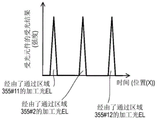
Fig. 10 is a graph showing the result of receiving processing light via a search mark.
Fig. 11 (a) is a plan view showing a search mark of a light receiving device assembled to an ideal assembly position, fig. 11 (b) is a plan view showing a search mark of a light receiving device assembled to a position different from the ideal assembly position, fig. 11 (c) is a graph showing a light receiving signal corresponding to a light receiving result of machining light passing through the search mark of the light receiving device assembled to the ideal assembly position, and fig. 11 (d) is a graph showing a light receiving signal corresponding to a light receiving result of machining light passing through the search mark of the light receiving device assembled to a position different from the ideal assembly position.
Fig. 12 (a) is a cross-sectional view showing a case where the processing head irradiates the processing light to the light receiving device for performing the focus control operation, fig. 12 (b) is a plan view showing a case where the processing head irradiates the processing light to the light receiving device for performing the focus control operation, and fig. 12 (c) is a graph showing a result of receiving the processing light by the light receiving element included in the light receiving device.
Fig. 13 is a plan view showing a stage on which a reference mark is formed.
Fig. 14 is a cross-sectional view showing an example of a machining base line and a measurement base line, and fig. 14 is a plan view showing an example of a machining base line and a measurement base line.
FIG. 15 is a plan view showing the relationship between the spot diameter of the machining light and the fine marks.
FIG. 16 is a plan view showing the relationship between the spot diameter of the processing light and the fine marks.
Fig. 17 is a plan view schematically showing the spot diameters of the machining light at respective positions on the surface of the workpiece when the machining light deflected by the galvanometer mirror and displaced by the f θ lens scans the surface of the workpiece.
Fig. 18 is a sectional view showing a positional relationship between the processing head and the light receiving device during the state detection operation, and fig. 18 (b) is a plan view showing a positional relationship between the processing head and the light receiving device during the state detection operation.
Fig. 19 (a) is a sectional view showing a positional relationship between the processing head and the light receiving device during the state detection operation, and fig. 19 (b) is a plan view showing a positional relationship between the processing head and the light receiving device during the state detection operation.
Fig. 20 is a plan view showing the irradiation position of the processing light on the surface of the workpiece (i.e., the surface along the XY plane) in a situation where no temperature drift occurs, and fig. 20 is a plan view showing the irradiation position of the processing light on the surface of the workpiece (i.e., the surface along the XY plane) in a situation where a temperature drift occurs.
Fig. 21 is a cross-sectional view showing the structure of a stage of the second embodiment.
Fig. 22 is a sectional view showing a method of arranging a light receiving device according to a third embodiment.
Fig. 23 is a sectional view showing the structure of a light receiving device according to a fourth embodiment.
Fig. 24 is a sectional view showing the structure of a light receiving device according to a fifth embodiment.
FIG. 25 is a plan view showing an example of a marker plate in FIG. 25A and FIG. 25B.
Fig. 26 is a system configuration diagram showing a system configuration of a machining system according to a sixth embodiment.
Fig. 27 is a sectional view showing the structure of a stage including a cover member.
FIG. 28 is a sectional view showing another example of the cover member.
FIG. 29 is a sectional view of a cover member not covering a beam passage member, shown in FIG. 29 (a) and FIG. 29 (b).
Fig. 30 is a perspective view showing the structure of an irradiation optical system according to a seventh embodiment.
Fig. 31 is a system configuration diagram showing a system configuration of a machining system according to the eighth embodiment.
Fig. 32 is a system configuration diagram showing a system configuration of a machining system according to the ninth embodiment.
Fig. 33 is a system configuration diagram showing a system configuration of a machining system according to the tenth embodiment.
Fig. 34 is a perspective view schematically showing the appearance of a processing system according to a tenth embodiment.
Fig. 35 is a system configuration diagram showing a system configuration of a machining system according to the eleventh embodiment.
Fig. 36 is a perspective view schematically showing the appearance of a machining system according to the eleventh embodiment.
Detailed Description
Embodiments of a machining system and a measuring member will be described below with reference to the drawings. Hereinafter, embodiments of the machining system and the measuring means will be described with reference to a machining system SYS for machining a workpiece W with machining light EL. However, the present invention is not limited to the embodiments described below.
In the following description, positional relationships of various components constituting the machining system SYS are described using an XYZ orthogonal coordinate system defined by X, Y, and Z axes orthogonal to each other. In the following description, for convenience of explanation, the X-axis direction and the Y-axis direction are respectively assumed to be a horizontal direction (i.e., a predetermined direction in a horizontal plane), and the Z-axis direction is assumed to be a vertical direction (i.e., a direction orthogonal to the horizontal plane, and substantially an up-down direction). The rotational directions (in other words, the tilt directions) around the X axis, the Y axis, and the Z axis are referred to as the θ X direction, the θ Y direction, and the θ Z direction, respectively. Here, the Z-axis direction may be a gravitational direction. Further, the XY plane may be set to the horizontal direction.
(1) Processing system SYSa of the first embodiment
First, a machining system SYS according to a first embodiment (hereinafter, the machining system SYS according to the first embodiment is referred to as a "machining system SYSa") will be described.
(1-1) Structure of processing System SYSa
First, the configuration of the machining system SYSa according to the first embodiment will be described with reference to fig. 1 and 2. Fig. 1 is a perspective view schematically showing an external appearance of a machining system SYSa according to a first embodiment. Fig. 2 is a system configuration diagram illustrating a system configuration of a machining system SYSa according to the first embodiment.
As shown in fig. 1 and 2, processing system SYSa includes processing apparatus 1, measurement apparatus 2, stage apparatus 3, and control apparatus 4. Machining device 1, measurement device 2, and stage device 3 are housed in a housing 5. However, machining device 1, measuring device 2, and stage device 3 may not be housed in housing 5. That is, machining system SYSa may not include housing 5 that houses machining device 1, measurement device 2, and stage device 3.
The machining apparatus 1 can machine the workpiece W under the control of the control apparatus 4. The workpiece W is an object to be machined by the machining apparatus 1. The workpiece W may be, for example, a metal, an alloy (e.g., duralumin), a semiconductor (e.g., silicon), a resin, a composite material such as Carbon Fiber Reinforced Plastic (CFRP), glass, ceramic, or any other material.
The machining apparatus 1 may perform a removal process of removing a part of the workpiece W by irradiating the workpiece W with the machining light EL. The removing process may also include at least one of a surface process, a cylinder process, a hole forming process, a smoothing process, a cutting process, and an engraving process (in other words, an imprint process) for forming an arbitrary character or an arbitrary pattern (in other words, engraving).
Here, an example of the removal process using the processing light EL will be described with reference to each of fig. 3 (a) to 3 (c). Fig. 3 (a) to 3 (c) are cross-sectional views each showing a case where the workpiece W is subjected to the removal processing. As shown in fig. 3 (a), the machining device 1 irradiates the machining light EL to a target irradiation area EA set (in other words, formed) on the surface of the workpiece W. When the processing light EL is irradiated to the target irradiation area EA, the energy of the processing light EL is transmitted to the target irradiation area EA and a portion close to the target irradiation area EA in the workpiece W. When heat is transferred by the energy of the processing light EL, the material constituting the target irradiation area EA and a portion close to the target irradiation area EA in the workpiece W is melted by the heat by the energy of the processing light EL. The molten material is scattered as droplets. Alternatively, the melted material is evaporated by heat due to the energy of the processing light EL. As a result, the target irradiation region EA and a portion close to the target irradiation region EA in the workpiece W are removed. That is, as shown in fig. 3 (b), a concave portion (in other words, a groove portion) is formed on the surface of the workpiece W. In this case, the machining device 1 machines the workpiece W by the principle of so-called hot working. Further, the machining apparatus 1 moves the target irradiation area EA on the surface of the workpiece W using a galvanometer mirror 1212 described later. That is, the machining device 1 scans the surface of the workpiece W with the machining light EL. As a result, as shown in fig. 3c, the surface of the workpiece W is at least partially removed along the scanning locus of the processing light EL (i.e., the movement locus of the target irradiation area EA). Therefore, the machining device 1 can appropriately remove a portion of the workpiece W to be subjected to the removal machining by scanning the machining light EL on the surface of the workpiece W along a desired scanning trajectory corresponding to the region to be subjected to the removal machining.
On the other hand, the machining device 1 can machine the workpiece W by the principle of non-thermal machining (for example, ablation machining) according to the characteristics of the machining light EL. That is, the machining device 1 may perform non-thermal machining (e.g., ablation machining) on the workpiece W. For example, when pulsed light having an emission time of picoseconds or less (or nanoseconds or femtoseconds or less as the case may be) is used as the processing light EL, materials constituting the target irradiation region EA and a portion close to the target irradiation region EA in the workpiece W are instantaneously evaporated and scattered. In addition, when pulsed light having an emission time of picoseconds or less (or nanoseconds or femtoseconds or less in some cases) is used as the processing light EL, the material constituting the target irradiation region EA and the portion close to the target irradiation region EA in the workpiece W may sublimate without passing through a molten state. Therefore, the concave portion (in other words, the groove portion) can be formed on the surface of the workpiece W while suppressing the influence of heat due to the energy of the processing light EL on the workpiece W as much as possible.
In the case of performing the removal processing, the processing apparatus 1 may form a rib (riblet) structure on the workpiece W. The rib structure may also be a structure capable of reducing the resistance of the surface of the workpiece W to fluid (particularly, at least one of frictional resistance and turbulent frictional resistance). The rib structure may also include a structure capable of reducing noise generated when the fluid moves relative to the surface of the workpiece W. The rib structure may also include, for example, a structure in which a plurality of grooves extending along a first direction (e.g., Y-axis direction) along the surface of the workpiece W are arranged along a second direction (e.g., X-axis direction) along the surface of the workpiece W and intersecting the first direction.
In the case of performing the removal processing, the processing apparatus 1 may form an arbitrary structure having an arbitrary shape on the surface of the workpiece W. As an example of the arbitrary structure, a structure in which a vortex is generated in the flow of the fluid on the surface of the workpiece W can be cited. As another example of the arbitrary structure, a structure for imparting hydrophobicity to the surface of the workpiece W may be cited. As another example of the arbitrary structure, a micro-nano-scale fine textured structure (typically, a textured structure) formed regularly or irregularly is exemplified. Such micro-texture structure may also include at least one of a shark skin structure and a dimple (dimple) structure having a function of reducing resistance caused by fluid (gas and/or liquid). The fine texture structure may also include a lotus leaf surface structure having at least one of a lyophobic function and a self-cleaning function, for example, having a lotus leaf effect. The fine texture structure may include at least one of a fine projection structure having a liquid transport function (see U.S. patent publication No. 2017/0044002), an uneven structure having a lyophilic function, an uneven structure having an antifouling function, a moth-eye (moth-eye) structure having at least one of a reflectance reduction function and a lyophobic function, an uneven structure in which only light of a specific wavelength is strengthened by interference to form a structural color, a pillar array (pilar array) structure having an adhesive function by van der Waals' force, an uneven structure having an aerodynamic noise reduction function, a honeycomb structure having a droplet trapping function, an uneven structure having improved adhesiveness to a layer formed on a surface, and the like.
In fig. 1 and 2 again, the machining apparatus 1 includes a machining light source 11, a machining head 12, a head drive system 13, and a position measuring device 14 in order to machine the workpiece W.
The processing light source 11 emits at least one of infrared light, visible light, ultraviolet light, and extreme ultraviolet light as the processing light EL, for example. However, other types of light may be used as the processing light EL. The processing light EL may also contain pulsed light (i.e., a plurality of pulsed beams). The processing light EL may be a laser. In this case, the processing light source 11 may include a Laser light source (e.g., a semiconductor Laser such as a Laser Diode (LD)). The laser light source may also comprise a fiber laser, CO 2 At least one of a laser, a Yttrium Aluminum Garnet (YAG) laser, and an excimer laser. However, the processing light EL may not be a laser. The machining Light source 11 may include any Light source (for example, at least one of a Light Emitting Diode (LED) and a discharge lamp).
The machining head 12 irradiates the workpiece W with the machining light EL from the machining light source 11. Therefore, the processing head 12 may also be referred to as an illumination device. In the example shown in fig. 1, a stage 32 on which a workpiece W can be placed is disposed below the processing head 12. Therefore, the machining head 12 emits the machining light EL downward from the machining head 12, and the machining light EL is irradiated to the workpiece W. In order to irradiate the processing light EL to the workpiece W, the processing head 12 includes an irradiation optical system 121. The irradiation optical system 121 will be described below with reference to fig. 4. Fig. 4 is a sectional view schematically showing the structure of the irradiation optical system 121.
As shown in fig. 4, the irradiation optical system 121 includes, for example, a focus changing optical system 1211, a galvanometer mirror 1212, and an f θ lens 1213.
The focus changing optical system 1211 is an optical member that can change the focus position of the processing light EL (i.e., the converging position of the processing light EL) along the traveling direction of the processing light EL. Therefore, the focus changing optical system 1211 can also be referred to as a beam converging position changing member. The focus changing optical system 1211 may include, for example, a plurality of lenses arranged along the traveling direction of the processing light EL. In this case, the focal position of the processing light EL may be changed by moving at least one of the lenses in the optical axis direction.
The processing light EL having passed through the focus changing optical system 1211 enters the galvanometer mirror 1212. The galvanometer mirror 1212 deflects the processing light EL (that is, changes the emission angle of the processing light EL), thereby changing the emission direction of the processing light EL from the galvanometer mirror 1212. Therefore, the galvanometer mirror 1212 may also be referred to as an emission direction changing member. When the emission direction of the processing light EL from the galvanometer mirror 1212 is changed, the position at which the processing light EL is emitted from the processing head 12 is changed. When the position at which the processing light EL is emitted from the processing head 12 is changed, the irradiation position of the processing light EL on the surface of the workpiece W is changed. Therefore, the galvanometer mirror 1212 can change (that is, can move) the irradiation position of the processing light EL on the surface of the workpiece W by deflecting the processing light EL. Therefore, the galvanometer mirror 1212 may also be referred to as an irradiation position moving member.
The galvanometer mirror 1212 includes, for example, an X scanning mirror 1212X and a Y scanning mirror 1212Y. The X-scanning mirror 1212X and the Y-scanning mirror 1212Y are movable optical members disposed on the optical path of the processing light EL between the processing light source 11 and the f θ lens 1213, respectively. The X-scanning mirror 1212X and the Y-scanning mirror 1212Y are each a variable inclination angle mirror whose angle with respect to the optical path of the processing light EL incident on each mirror is variable. The X scanning mirror 1212X reflects the processing light EL toward the Y scanning mirror 1212Y. The X-scan mirror 1212X can oscillate or rotate about a rotation axis along the Y-axis. By the oscillation or rotation of the X scanning mirror 1212X, the machining light EL scans the surface of the workpiece W along the X-axis direction. By the oscillation or rotation of the X scanning mirror 1212X, the target irradiation area EA is moved in the X-axis direction on the surface of the workpiece W. The Y scan mirror 1212Y reflects the processing light EL toward the f θ lens 1213. The Y scan mirror 1212Y can oscillate or rotate about a rotational axis along the X axis. The machining light EL scans the surface of the workpiece W in the Y-axis direction by the oscillation or rotation of the Y-scanning mirror 1212Y. By the oscillation or rotation of the Y scanning mirror 1212Y, the target irradiation area EA is moved in the Y-axis direction on the surface of the workpiece W.
With such a galvanometer mirror 1212, the processing light EL can scan a processing emission area PSA determined with respect to the processing head 12. That is, the target irradiation area EA can be moved within the processing emission area PSA with reference to the processing head 12 by the galvanometer mirror 1212. The machining emission region PSA indicates a region (in other words, a range) in which machining is performed by the machining device 1 with the positional relationship between the machining head 12 and the workpiece W fixed (i.e., without modification). Typically, the machining emission region PSA is set to coincide with or be narrower than a scanning range of the machining light EL deflected by the galvanometer mirror 1212 in a state in which the positional relationship between the machining head 12 and the workpiece W is fixed. When the machining emission region PSA is smaller than a portion of the workpiece W to be machined, the following steps are repeated: an operation of scanning a machining emission region PSA set in a certain portion of the workpiece W with the machining light EL to machine the certain portion of the workpiece W, and an operation of changing the relative positional relationship between the machining head 12 and the workpiece W to change the position of the machining emission region PSA on the workpiece W.
The irradiation optical system 121 may include any optical member that can deflect the processing light EL (that is, can change at least one of the emission direction and the irradiation position of the processing light EL) in addition to the galvanometer mirror 1212 or instead of the galvanometer mirror 1212. As an example of such an optical member, a polygon mirror having a plurality of reflection surfaces with different angles is cited. The polygon mirror is rotatable while the processing light EL is irradiated onto a reflection surface to change an incident angle of the processing light EL with respect to the reflection surface and switch the reflection surface onto which the processing light EL is irradiated among the plurality of reflection surfaces.
The f θ lens 1213 is an optical system for emitting the processing light EL from the galvanometer mirror 1212 toward the workpiece W. In particular, the f θ lens 1213 is an optical element that can condense the processing light EL from the galvanometer mirror 1212 to a light condensing surface. Therefore, the f θ lens 1213 may also be referred to as a condensing optical system. The light-converging surface of the f θ lens 1213 may be set to the surface of the workpiece W, for example. At this time, the f θ lens 1213 can condense the processing light EL from the galvanometer mirror 1212 to the surface of the workpiece W.
Again in fig. 1 and 2, the head driving system 13 moves the processing head 12 in at least one of the X-axis direction, the Y-axis direction, the Z-axis direction, the θ X direction, the θ Y direction, and the θ Z direction. Fig. 1 shows an example in which the head drive system 13 moves the processing head 12 in the Z-axis direction. At this time, the head driving system 13 may also include, for example, a Z slider member 131 extending in the Z-axis direction. The Z slider member 131 is disposed on a support frame 6, and the support frame 6 is disposed on a platen 31 described later via an anti-vibration device. The support frame 6 may also comprise, for example: a pair of leg members 61 arranged on the platen 31 via an anti-vibration device and extending in the Z-axis direction; and a beam member 62 that is disposed on the pair of leg members 61 so as to connect the upper end portions of the pair of leg members 61 and extends in the X-axis direction. The Z slider member 131 is disposed on the beam member 62 via a support member 63 extending in the Z-axis direction, for example. The processing head 12 is connected to the Z slider member 131 so as to be movable along the Z slider member 131.
When the processing head 12 moves, the positional relationship between the processing head 12 and the stage 32 (and further, the workpiece W placed on the stage 32) changes. Therefore, moving the machining head 12 is equivalent to changing the positional relationship between the machining head 12 and each of the stage 32 and the workpiece W.
The position measuring device 14 may measure (in other words, may detect) the position of the processing head 12. The position measuring device 14 may include at least one of an encoder and a laser interferometer, for example.
The measuring device 2 can measure the workpiece W under the control of the control device 4. For measuring the workpiece W, the measuring device 2 comprises a measuring head 21, a head drive system 22 and a position measuring device 23.
The measuring head 21 can measure the workpiece W under the control of the control device 4. For example, the measuring head 21 may be a device that can measure the state of the workpiece W. The state of the work W may also include the position of the work W. The position of the workpiece W may also include the position of the surface of the workpiece W. The position of the surface of the workpiece W may include the position of each surface portion, which is obtained by subdividing the surface of the workpiece W, in at least one of the X-axis direction, the Y-axis direction, and the Z-axis direction. The state of the work W may also include the shape (e.g., three-dimensional shape) of the work W. The shape of the workpiece W may also include the shape of the surface of the workpiece W. The shape of the surface of the workpiece W may include, in addition to or instead of the position of the surface of the workpiece W, a direction of each surface portion that subdivides the surface of the workpiece W (for example, a direction of a normal line of each surface portion, which is substantially equivalent to an inclination amount of each surface portion with respect to at least one of the X axis, the Y axis, and the Z axis). Measurement information relating to the measurement result of the measurement head 21 is output from the measurement head 21 to the control device 4.
The measuring head 21 measures the workpiece W in units of the measuring emission area MSA. The measurement emission area MSA indicates an area (in other words, a range) where measurement by the measurement head 21 is performed in a state where the positional relationship between the measurement head 21 and the workpiece W is fixed (i.e., not changed). The measurement emission area MSA may also be referred to as the measurable range, measurable area of the measuring head 21.
The measuring head 21 may also measure the workpiece W optically. That is, the measuring head 21 may measure the workpiece W using an arbitrary measuring beam such as measuring light. For example, the measurement head 21 may also measure the workpiece W using a light sectioning method, which is a method of projecting slit light onto the surface of the workpiece W and measuring the shape of the projected slit light. For example, the measuring head 21 may measure the workpiece W by using a white interference method of measuring an interference pattern of white light having passed through the workpiece W and white light not having passed through the workpiece W. For example, the measurement head 21 may measure the workpiece W using at least one of a pattern projection method of projecting a light pattern onto the surface of the workpiece W and measuring the shape of the projected pattern, a time of flight (time of flight) method of projecting light onto the surface of the workpiece W, a method of measuring the distance to the workpiece W from the time until the projected light returns, and a method of performing this operation at a plurality of positions on the workpiece W, a moire (moire) method (specifically, a grating irradiation method or a grating projection method), a holographic interference method, an auto collimation (auto collimation) method, a stereo method, an astigmatism method, a critical angle method, a knife edge (knife-edge) method, an interferometry method, and a confocal method. For example, the measurement head 21 may also measure the workpiece W by photographing the workpiece W illuminated by the illumination light. In either case, the measuring head 21 may also comprise: a light source that emits measurement light ML (for example, slit light, white light, or illumination light); and a light receiver that receives light from the workpiece W to which the measurement light ML is irradiated (for example, reflected light of the measurement light).
The head driving system 22 moves the measuring head 21 in at least one of an X-axis direction, a Y-axis direction, a Z-axis direction, a ox-direction, a oy-direction, and a oz-direction. Fig. 1 shows an example in which the head drive system 22 moves the measurement head 21 in the Z-axis direction. At this time, the head drive system 22 may also include, for example, a Z slider member 221 extending in the Z-axis direction. The Z slider member 221 may be disposed on the beam member 62 via a support member 64 extending in the Z-axis direction. The measuring head 21 is connected to the Z slider member 221 in a manner movable along the Z slider member 221.
When the measurement head 21 moves, the positional relationship between the measurement head 21 and the stage 32 (and further, the workpiece W mounted on the stage 32) changes. Therefore, moving the measurement head 21 is equivalent to changing the positional relationship between the measurement head 21 and each of the stage 32 and the workpiece W.
The position measuring device 23 may measure (in other words, may detect) the position of the measuring head 21. The position measuring device 23 may include at least one of an encoder and a laser interferometer, for example.
The platen 31 is disposed on a bottom surface of the housing 5 (or on a support surface such as a floor surface on which the housing 5 is placed). A stage 32 is disposed on the platen 31. An anti-vibration device, not shown, for reducing transmission of vibration of the platen 31 to the stage 32 may be provided between the platen 31 and a support surface such as a bottom surface of the frame 5 or a floor surface on which the frame 5 is placed. Further, the above-described support frame 6 may be disposed on the platen 31.
The stage 32 is a mounting device on which the workpiece W is mounted. The stage 32 may be capable of holding the workpiece W mounted on the stage 32. Alternatively, the stage 32 may not be able to hold the workpiece W placed on the stage 32. At this time, the workpiece W may be placed on the stage 32 without a clamp (clamp-less).
When the stage 32 moves, the positional relationship between the stage 32 and the workpiece W, and the processing head 12 and the measurement head 21, respectively, changes. Thus, moving the stage 32 is equivalent to changing the positional relationship between the stage 32 and the workpiece W, and the processing head 12 and the measurement head 21, respectively.
The light receiving device 35 includes a light receiving unit that can receive the processing light EL from the processing head 12. Further, the light receiving device 35 includes a measuring member that the measuring head 21 can measure. The result of the light reception by the light receiving device 35 of the processing light EL and the result of the measurement by the measurement head 21 of the light receiving device 35 are used to control the operation of the processing system SYSa. The structure of the light receiving device 35 will be described in detail below with reference to fig. 5 to 7.
The control device 4 controls the operation of the machining system SYSa. For example, control device 4 may set the machining conditions for workpiece W and control machining device 1 and stage device 3 to machine workpiece W in accordance with the set machining conditions.
The control device 4 controls the operation of the machining system SYSa. The control device 4 may include, for example, an arithmetic device and a storage device. The computing device may include at least one of a Central Processing Unit (CPU) and a Graphics Processing Unit (GPU), for example. The storage device may also include a memory, for example. The control device 4 functions as a device for controlling the operation of the processing system SYSa by executing the computer program by the arithmetic device. The computer program is a computer program for causing the arithmetic device to perform (i.e., execute) an operation to be described later to be performed by the control device 4. That is, the computer program is a computer program for causing the control device 4 to function so as to cause the machining system SYS to perform an operation described later. The computer program executed by the arithmetic device may be recorded in a storage device (i.e., a recording medium) included in the control device 4, or may be recorded in any storage medium (e.g., a hard disk or a semiconductor memory) incorporated in the control device 4 or externally provided to the control device 4. Alternatively, the arithmetic device may download a computer program to be executed from a device external to the control device 4 via a network interface.
The control device 4 may not be provided inside the processing system SYSa. For example, the control device 4 may be provided as a server or the like outside the machining system SYSa. In this case, the control device 4 and the machining system SYSa may be connected by a wired and/or wireless network (or a data bus and/or a communication line). For example, a network using a Serial Bus type interface represented by at least one of Institute of Electrical and Electronics Engineers (IEEE) 1394, RS-232x, RS-422, RS-423, RS-485, and Universal Serial Bus (USB) may be used as the wired network. As a wired network, a network using an interface of a parallel bus system may be used. As the wired network, a network using an interface conforming to ethernet (registered trademark) typified by at least one of 10BASE-T, 100BASE-TX, and 1000BASE-T may be used. As a wireless network, a network using radio waves may be used. An example of a Network using radio waves is a Network conforming to ieee802.1x (for example, at least one of a Local Area Network (LAN) and Bluetooth (registered trademark)). As a wireless network, a network using infrared rays may be used. As a wireless network, a network using optical communication may be used. In this case, the control device 4 and the machining system SYSa may be configured to be able to transmit and receive various information via a network. The control device 4 may be configured to transmit information such as commands and control parameters to the machining system SYSa via a network. The processing system SYSa may also include a receiving device that receives information such as commands or control parameters from the control device 4 via the network. The machining system SYSa may include a transmission device that transmits information such as a command and a control parameter to the control device 4 via the network (i.e., an output device that outputs information to the control device 4). Alternatively, a first control device that performs a part of the processes performed by the control device 4 may be provided inside the processing system SYSa, and a second control device that performs another part of the processes performed by the control device 4 may be provided outside the processing system SYSa.
As a recording medium for recording the computer program executed by the control device 4, at least one of a semiconductor Memory such as a Compact Disc Read Only Memory (CD-ROM), a Compact Disc-Recordable (CD-R), a Compact Disc-Rewritable (CD-RW), a floppy disk, a Magneto-Optical disk (MO), a Digital Versatile Disc Read Only Memory (DVD-ROM), a Random Access Digital Versatile Disc (DVD-RAM), a Digital Versatile Disc Recordable (DVD-Recordable), a DVD + R, a Rewritable Digital Versatile Disc (DVD-Recordable), a DVD + R, a semiconductor Memory such as a DVD-Recordable (DVD-Recordable), a Blu-ray Disc (RW), and other Recordable (USB-Recordable) media, and a Blu-ray Disc may be used. The recording medium may include a machine that can record a computer program (for example, a general-purpose machine or a dedicated machine that is installed with a computer program in a state that the computer program can be executed in at least one form of software, firmware, or the like). Further, each process or function included in the computer program may be realized by a logical processing block realized in the control device 4 by the control device 4 (that is, a computer) executing the computer program, may be realized by hardware such as a predetermined gate array (FPGA, ASIC) included in the control device 4, or may be realized by a form in which the logical processing block and a local hardware module realizing a part of elements of the hardware are mixed.
(1-2) Structure of light receiving device 35
Next, the configuration of light receiving device 35 included in stage device 3 will be described with reference to fig. 5 to 7. Fig. 5 is a plan view showing the arrangement position of the light receiving device 35. Fig. 6 is a sectional view showing the structure of the light receiving device 35. Fig. 7 is a plan view showing the structure of the light receiving device 35. FIG. 6 is a sectional view taken along line VII-VII' of FIG. 7.
As shown in fig. 5, light receiving device 35 is disposed on stage 32. The light receiving device 35 may be disposed at a position different from the placement surface 321 on which the workpiece W is placed on the stage 32. For example, the light receiving device 35 may be disposed at a position shifted from the placement surface 321 in at least one of the X-axis direction and the Y-axis direction on the stage 32. For example, the light receiving device 35 may be disposed on the outer peripheral surface 322 of the stage 32 located outside the placement surface 321 (more specifically, a member of the stage 32 on which the outer peripheral surface 322 is a surface). However, the light receiving device 35 may be disposed on the mounting surface 321 (more specifically, the mounting surface 321 of the stage 32 is a surface member). Light receiving device 35 may be disposed at any position of stage 32. At least a part of light receiving device 35 may be detachable from stage 32. Alternatively, light receiving device 35 may be integrated with stage 32. Further, a plurality of light receiving devices 35 may be arranged on stage 32. At this time, one of the plurality of light receiving devices 35 may be disposed at the end in the-X direction and the end in the + Y direction of outer circumferential surface 322 of stage 32 shown in fig. 5, and the other of the plurality of light receiving devices 35 may be disposed at the end in the + X direction and the end in the-Y direction of outer circumferential surface 322. That is, at least two of the plurality of light receiving devices 35 may be arranged at opposite corners of the stage 32. Further, the plurality of light receiving devices 35 may be arranged at four corners of the stage 32. In addition, stage 32 may also be referred to as a platform.
As shown in fig. 6, the light receiving device 35 includes a beam passage member 351 and a light receiving element 352. The beam passage member 351 is a plate-like member along the XY plane. The beam passage member 351 in the XY plane has a rectangular shape, but may have any other shape (e.g., a circular shape or an elliptical shape). The beam passage member 351 has a side dimension of several mm to ten mm, for example, but may have another dimension. The light receiving element 352 includes a light receiving surface 3521 extending along the XY plane. The light-receiving surface 3521 in the XY plane has a rectangular shape, but may have any other shape (for example, a circular shape or an elliptical shape). The dimension of one side of the light receiving surface 3521 may be the same as the dimension of one side of the beam passage member 351, may be smaller than the dimension of one side of the beam passage member 351, or may be larger than the dimension of one side of the beam passage member 351.
The beam passage member 351 and the light receiving element 352 are arranged inside a recess 323 (i.e., a concave portion) formed in the stage 32. That is, the beam passage member 351 and the light receiving element 352 are arranged in the recess 323 recessed from the outer peripheral surface 322 toward the-Z side. Since the light receiving device 35 is disposed on the outer peripheral surface 322 as described above, the concave portions 323 are formed on the outer peripheral surface 322. However, at least one of the beam passage member 351 and the light receiving element 352 may be disposed at a position different from the pit 323.
In the pit 323, the beam passage member 351 is arranged above the light receiving element 352. That is, the beam passage member 351 is disposed closer to the machining head 12 and the measuring head 21 than the light receiving element 352. At this time, as shown in fig. 6, the surface of beam passage member 351 (specifically, the surface facing toward processing head 12 and measuring head 21, the surface on the + Z side) may be located below outer peripheral surface 322 (that is, the surface of stage 32). At this time, since the light receiving device 35 does not protrude from the surface of the stage 32, the workpiece W placed on the stage 32 is less likely to erroneously contact the light receiving device 35 (particularly, the beam passage member 351). As a result, the workpiece W contacts the beam passage member 351, and the beam passage member 351 is less likely to be damaged or contaminated. However, the surface of the beam passage member 351 may be located at the same height as the outer peripheral surface 322 and may be located above the outer peripheral surface 322.
The beam passing member 351 includes a glass substrate 3511 and an attenuation film 3512, the attenuation film 3512 being formed on at least a part of a surface of the glass substrate 3511. The attenuation film 3512 is a member that can attenuate the processing light EL incident on the attenuation film 3512. The "attenuation of the processing light EL by the attenuation film 3512" in the first embodiment includes not only the case where the intensity of the processing light EL passing through the attenuation film 3512 is smaller than the intensity of the processing light EL entering the attenuation film 3512, but also the case where the processing light EL entering the attenuation film 3512 is shielded (i.e., shielded). Therefore, when the processing light EL enters the attenuation film 3512, the processing light EL attenuated by the attenuation film 3512 enters the light receiving element 352 through the attenuation film 3512, or the processing light EL is blocked by the attenuation film 3512 and does not enter the light receiving element 352. The attenuation film 3512 may be formed of a chromium film or a chromium oxide film.
At least one opening 353 is formed in the attenuation film 3512. In the example shown in fig. 6, a plurality of openings 353 are formed in the attenuation film 3512. The opening 353 is a through hole penetrating the attenuation film 3512 in the Z-axis direction. Therefore, when the processing light EL enters the opening 353 formed in the attenuation film 3512, the processing light EL passes through the beam passage member 351 via the opening 353. That is, the processing light EL is incident on the light receiving element 352 through the opening 353 without being attenuated or blocked by the attenuation film 3512.
In this way, the portion of the glass substrate 3511 where the attenuation film 3512 is formed (i.e., the portion where the opening 353 is not formed) functions as the attenuation region 354 which attenuates the processing light EL. On the other hand, a portion of the glass substrate 3511 where the attenuation film 3512 is not formed (i.e., a portion where the opening 353 is formed) functions as the passage region 355 through which the processing light EL passes. At this time, the processing light EL passing through the passing region 355 is not attenuated by the passing region 355. However, the processing light EL passing through the region 355 may also pass through the region 355. That is, the passing region 355 may not be a region through which all (i.e., 100%) of the processing light EL incident on the passing region 355 passes, but may be a region through which a part of the processing light EL incident on the passing region 355 passes. However, the attenuation ratio of the passing region 355 to the processing light EL is smaller than that of the attenuation region 354 to the processing light EL. Typically, the attenuation region 354 is disposed adjacent to the pass-through region 355. That is, the attenuation region 354 is disposed between the plurality of passage regions 355 formed by the plurality of openings 353, respectively. The plurality of pass-through regions 355 are configured in the attenuation region 354. As described above, when the surface of beam passage member 351 is located below outer peripheral surface 322 (i.e., the surface of stage 32), the portion of beam passage member 351 that functions as attenuation region 354 and the portion of beam passage member 351 that functions as passage region 355 are also located below outer peripheral surface 322 (i.e., the surface of stage 32).
At least one of the plurality of passing areas 355 formed by the plurality of openings 353, respectively, may also be formed as a mark (i.e., a pattern) 356 having a predetermined shape in a plane (typically, XY plane) along the surface of the attenuation film 3512. The marker 356 is measured by the measuring head 21. Thus, the beam passing member 351 formed with the marker 356 measurable by the measuring head 21 may also be referred to as a measuring member.
For example, as shown in fig. 7, a slit mark 356-1 as an example of the mark 356 may be formed on the beam passage member 351. The slit mark 356-1 is a mark formed by the passing region 355 having a single linear (e.g., slit-like) shape in a plane along the surface of the attenuating film 3512. The length (i.e., the dimension in the longitudinal direction) of the linear passage area 355 forming the slit mark 356-1 is, for example, 0.1mm to 1mm, but may be other lengths. The width (i.e., the dimension in the short side direction) of the linear passing region 355 forming the slit mark 356-1 is, for example, several μm, but may be other lengths. In the example shown in fig. 7, the beam passage member 351 is formed with a plurality of slit marks 356-1 having different angles with respect to the X axis and the Y axis. In the example shown in fig. 7, a plurality of slit marks 356-1 are arranged along the Y-axis direction, but a plurality of slit marks 356-1 may be formed at arbitrary positions. However, a single slit mark 356-1 may be formed on the beam passage member 351.
For example, as shown in fig. 7, a fine mark 356-2 as an example of the mark 356 may be formed on the beam passage member 351. The fine mark 356-2 is a mark formed of a plurality of linear passing regions 355 each extending in one direction and arranged in another direction intersecting the one direction. The length (i.e., the dimension in the longitudinal direction) of the linear passing region 355 forming the fine mark 356-2 is, for example, 0.1mm to 1mm, but may be other lengths. The width (i.e., the dimension in the short-side direction) of the linear passing region 355 forming the fine mark 356-2 is, for example, several μm, but may be another width. The beam passage member 351 may be formed with a plurality of fine marks 356-2 having different linear passage regions 355 extending in different directions. For example, as shown in fig. 7, the beam passage member 351 may include: a fine mark 356-2 formed by a plurality of linear passage areas 355 extending in the Y-axis direction and arranged in the X-axis direction, respectively, and a fine mark 356-2 formed by a plurality of linear passage areas 355 extending in the X-axis direction and arranged in the Y-axis direction, respectively. Further, the beam passage member 351 may be formed with a plurality of fine marks 356-2 having different arrangement pitches of the plurality of linear passage regions 355 (i.e., intervals between two adjacent passage regions 355). For example, as shown in fig. 7, the beam passage member 351 may be formed with: a fine mark 356-2 formed by arranging a plurality of line-shaped passing regions 355 at a first pitch, and a fine mark 356-2 formed by arranging a plurality of line-shaped passing regions 355 at a second pitch smaller than the first pitch. In the example shown in FIG. 7, the plurality of fine marks 356-2 are arranged along the Y-axis direction, but the plurality of fine marks 356-2 may be formed at arbitrary positions. However, a single fine mark 356-2 may also be formed in the beam-passing structure 351.
For example, as shown in fig. 7, a rectangular mark 356-3 as an example of the mark 356 may be formed on the beam passage member 351. The rectangular mark 356-3 is a mark formed by a pass region 355 having a rectangular shape in a plane along the surface of the attenuation film 3512. The size of the rectangular passing region 355 forming the rectangular mark 356-3 is, for example, 0.1 μm to several tens of μm, but may be other sizes. The beam passage member 351 may be formed with a plurality of rectangular marks 356-3 having different sizes of the passage region 355 (for example, sizes in at least one of the X-axis direction and the Y-axis direction). In the example shown in FIG. 7, a plurality of rectangular marks 356-3 are arranged along the Y-axis direction, but a plurality of rectangular marks 356-3 may be formed at arbitrary positions. However, a single rectangular mark 356-3 may be formed on the beam passage member 351.
For example, as shown in fig. 7, a cross mark 356-4 may be formed on the beam passage member 351 as an example of the mark 356. The cross mark 356-4 is a mark formed of a plurality of linear passage areas 355 each extending in a first direction and arranged in a second direction intersecting the first direction, and a plurality of linear passage areas 355 each extending in a third direction intersecting the first direction and arranged in a fourth direction intersecting the third direction. In the example shown in fig. 7, the cross mark 356-4 is a mark formed of a plurality of linear passage areas 355 each extending in the X-axis direction and arranged in the Y-axis direction, and a plurality of linear passage areas 355 each extending in the Y-axis direction and arranged in the X-axis direction. In this case, the cross mark 356-4 may be regarded as a grid-like mark. The width (i.e., the dimension in the short-side direction) of the linear passing region 355 forming the cross mark 356-4 is, for example, several μm to several tens μm, but may be another width. The size of the cross mark 356-4 (e.g., the size in at least one of the X-axis direction and the Y-axis direction) is, for example, 0.1mm to several mm, but may be other sizes. The beam passage member 351 may be formed with a plurality of cross marks 356-4 having different arrangement pitches of the linear passage regions 355 (i.e., intervals between two adjacent passage regions 355). When the cross mark 356-4 is a grid mark, if the arrangement pitch of the plurality of linear passing areas 355 changes, the number of grids formed by the cross mark 356-4 changes. Therefore, a plurality of cross marks 356-4 having different numbers of grids may be formed on the beam passage member 351. In the example shown in fig. 7, a plurality of cross marks 356-4 are arranged along the Y-axis direction, but a plurality of cross marks 356-4 may be formed at arbitrary positions. However, a single cross mark 356-4 may be formed on the beam passage member 351.
For example, as shown in fig. 7, a search mark 356-5 as an example of the mark 356 may be formed on the beam passage member 351. The search mark 356-5 is a mark formed of two first linear passage areas 355 each extending in the fifth direction and spaced apart in the sixth direction orthogonal to the fifth direction, and a second linear passage area 355 extending in the seventh direction inclined (i.e., obliquely intersecting) with respect to the fifth direction. In the example shown in fig. 7, the search mark 356-5 is a mark formed of two first linear passage areas 355 each extending in the Y axis direction and spaced apart in the X axis direction, and a second linear passage area 355 disposed between the two first linear passage areas 355 and extending in a direction inclined with respect to the Y axis direction. The length (i.e., the dimension in the longitudinal direction) of the first linear passage area 355 forming the search marker 356-5 is, for example, 0.1mm to 1mm, but may be another length. The width (i.e., the dimension in the short side direction) of the linear passing region 355 forming the search mark 356-5 is, for example, several μm, but may be other widths. The size of the search flag 356-5 (e.g., the size in at least one of the X-axis direction and the Y-axis direction) is, for example, 0.1mm to several mm, but may be other sizes. The distance between the two first linear passing areas 355 forming the search marker 356-5 is, for example, 0.1mm to 1mm, but other distances are also possible. The angle formed by the first linear passage area 355 and the second linear passage area 355 inclined with respect to the first linear passage area 355 is 10 degrees to 20 degrees (for example, 15 degrees), but may be other angles. In the example shown in FIG. 7, a plurality of search marks 356-5 are formed around the other marks 356 than the search mark 356-5, but a plurality of search marks 356-5 may be formed at arbitrary positions.
The light-receiving element 352 is a light-receiving portion that can receive (e.g., detect) the processing light EL incident on the light-receiving element 352 via the passing region 355 (i.e., the opening 353) by using the light-receiving surface 3521. The light receiving element 352 is a light receiving portion that can receive the processing light EL that has passed through the pass region 355 (i.e., the opening 353) by using the light receiving surface 3521. As an example of the light receiving unit, a photoelectric converter that photoelectrically converts the received processing light EL is given.
The light receiving element 352 can receive the processing light EL incident on the light receiving element 352 via each of the plurality of passage regions 355 on the light receiving surface 3521. The light-receiving surface 3521 may be formed by one photoelectric conversion surface of the photoelectric conversion element. For example, the light receiving element 352 may receive the processing light EL incident on the light receiving element 352 via the first passing region 355 (e.g., the passing region 355 constituting the one slit mark 356-1) by the first portion of the light receiving surface 3521. For example, the light receiving element 352 may receive the processing light EL incident on the light receiving element 352 via the second passage area 355 (for example, the passage area 355 constituting the other slit mark 356-1 different from the one slit mark 356-1) by the second portion of the light receiving surface 3521. For example, the light receiving element 352 may receive the processing light EL incident on the light receiving element 352 via the third passing region 355 (e.g., the passing region 355 constituting one fine mark 356-2) by the third portion of the light receiving surface 3521. As described above, in the first embodiment, the light receiving device 35 does not include the plurality of light receiving elements 352 corresponding to the plurality of passing regions 355. The light receiving device 35 may include a light receiving element 352 common to the plurality of passing regions 355. However, the light receiving device 35 may include a plurality of light receiving elements 352 corresponding to the plurality of passing regions 355, respectively.
When the light receiving element 352 receives the processing light EL through the pass region 355, the focus position of the processing light EL may be set at or near the pass region 355 of the beam passing member 351. On the other hand, in the case where the workpiece W is machined by the machining light EL, the focal position of the machining light EL may be set on the surface of the workpiece W or in the vicinity thereof. Therefore, the control device 4 may set the focus position of the processing light EL to an appropriate position by controlling the focus changing optical system 1211. At this time, the control device 4 may control the focus position of the processing light EL based on information on the distance between the surface of the stage 32 (for example, the mounting surface 321 or the outer peripheral surface 322) and the light receiving surface 3521 (in particular, the distance in the Z-axis direction corresponding to the traveling direction of the processing light EL). For example, when the state of the processing system SYSa is switched between a state in which the workpiece W is processed by the processing light EL and a state in which the light-receiving element 352 receives the processing light EL via the passing region 355, the control device 4 may move the focus position of the processing light EL by a change amount according to the distance between the surface of the stage 32 (for example, the mounting surface 321 or the outer peripheral surface 322) and the light-receiving surface 3521.
Considering the case where the workpiece W is processed by irradiation of the processing light EL, at least a part of the light receiving device 35 may be processed (substantially damaged) by the irradiation of the processing light EL. Therefore, the intensity of machining light EL (e.g., the amount of energy per unit area in a plane intersecting the traveling direction of machining light EL) may be controlled so that the intensity of machining light EL (e.g., the amount of energy per unit area on light-receiving surface 3521 of light-receiving element 352) applied to light-receiving device 35 is smaller than the intensity of machining light EL applied to workpiece W (e.g., the amount of energy per unit area on the surface of workpiece W) for machining workpiece W. In this case, the processing light source 11 itself may be controlled to reduce the intensity of the processing light EL, or a light extinction member (not shown) disposed on the emission side of the processing light source 11 may be controlled to reduce the intensity of the processing light EL.
The light reception result of the light receiving element 352 includes information on the state of the processing light EL incident on the light receiving element 352. For example, the light reception result of the light receiving element 352 includes information on the intensity of the processing light EL incident on the light receiving element 352 (specifically, the intensity in the plane intersecting the XY plane). More specifically, the light reception result of the light receiving element 352 includes information on the intensity distribution of the processing light EL in the plane along the XY plane. The result of light reception by the light receiving element 352 is output to the control device 4.
In addition, as described above, when the marker 356 is measured by the measuring head 21, the measurement result of the marker 356 by the measuring head 21 is output to the control device 4.
The control device 4 controls the processing system SYSa (for example, at least one of the processing device 1, the measuring device 2, and the stage device 3) based on at least one of the result of receiving the processing light EL by the light receiving element 352 and the result of measuring the mark 356 by the measuring head 21 so that the processing system SYSa can appropriately process the workpiece W. That is, the processing system SYSa controls the processing system SYSa (for example, at least one of the processing apparatus 1, the measuring apparatus 2, and the stage apparatus 3) using the light receiving apparatus 35 so that the processing system SYSa can appropriately process the workpiece W. The following further describes a usage mode of the light receiving device 35 used to control the processing system SYSa.
(1-2) utilization form of light receiving device 35
In one embodiment, for example, controller 4 may perform an assembly error measurement operation for measuring an assembly error of light receiving device 35 with respect to stage 32 based on the result of receiving processing light EL via pass area 355 constituting search mark 356-5. For example, the control device 4 may perform a focus control operation for controlling the focus position of the processing light EL based on the result of receiving the processing light EL through the passing region 355 constituting the slit mark 356-1. For example, the control device 4 may perform a B-CHK operation (baseline measurement operation) of measuring the distance (so-called baseline) between the device origin AO of the processing system SYSa and each of the processing origin PO and the measurement origin MO based on the result of light reception of the processing light EL via the passing area 355 constituting the fine mark 356-2 and the result of measurement of the cross mark 356-4 by the measurement head 21. For example, the controller 4 may perform an optical state control operation for suppressing an influence due to a variation in the state (for example, beam profile) of the processing light EL scanning the surface of the workpiece W based on the light reception result of the processing light EL passing through the pass region 355 constituting the slit mark 356-1. For example, the control device 4 may perform a galvano control operation, which is one of the phenomena that the irradiation position of the processing light EL in the plane along the XY plane is deviated due to the temperature (i.e., heat) of the galvano mirror 1212, on the basis of the light reception result of the processing light EL via the passing region 355 constituting the slit mark 356-1, to reduce the influence of the temperature drift of the galvano mirror 1212.
The control device 4 may perform at least a part of these operations (for example, the assembly error measurement operation, the focus control operation, the B-CHK operation, the optical state control operation, and the current detection control operation) before starting the irradiation of the processing light EL to the workpiece W for the removal processing. The control device 4 may perform at least part of these operations after the irradiation of the workpiece W with the processing light EL is completed to perform the removal processing. The control device 4 may perform at least a part of these operations during at least a part of the period in which the workpiece W is irradiated with the processing light EL for the removal processing.
The assembly error measurement operation, focus control operation, B-CHK operation, optical state control operation, and current detection control operation will be described in order below.
(1-2-1) Assembly error measurement action
First, an assembly error of light receiving device 35 with respect to stage 32 will be described with reference to fig. 8. Fig. 8 is a plan view showing light receiving device 35 in which an assembly error with respect to stage 32 occurs.
As shown in fig. 7, the light receiving device 35 may be assembled at a position different from an ideal assembly position (i.e., an assembly position in design). For example, the light receiving device 35 may be mounted at a position deviated from an ideal mounting position in the X-axis direction. For example, the light receiving device 35 may be mounted at a position deviated from an ideal mounting position in the Y-axis direction. For example, the light receiving device 35 may be assembled at a position deviated in the θ Z direction from the ideal assembly position (i.e., a position rotated about the Z axis from the ideal assembly position).
In order to measure the assembly error of the light receiving device 35 as described above, the control device 4 acquires the light receiving result of the processing light EL via the passing region 355 constituting the search mark 356-5. Specifically, the control device 4 controls the stage drive system 33 to move the stage 32 to a position at which the processing head 12 can irradiate the processing light EL to one search mark 356-5 of the plurality of search marks 356-5 when the light receiving device 35 is assembled at the desired assembly position. That is, the control device 4 moves the stage 32 so that one search mark 356-5 is located within the process emission area PSA. In this case, the control device 4 may move the machining head 12 in addition to or instead of the stage 32. Subsequently, the control device 4 controls the processing head 12 to irradiate the processing light EL to one search mark 356-5. At this time, as shown in fig. 9 which is a plan view showing the scanning locus of the processing light EL irradiated to the search mark 356-5, the control device 4 scans the search mark 356-5 with the processing light EL in a direction intersecting with the three linear passage areas 355 forming the search mark 356-5 so that the processing light EL is sequentially irradiated to the three linear passage areas 355 forming the search mark 356-5. That is, the irradiation position of the processing light EL on the beam passage member 351 where the search mark 356-5 is formed (i.e., the position of the processing light EL with respect to the beam passage member 351) changes along the direction in which the three linear passage regions 355 forming the search mark 356-5 are arranged. Specifically, as described above, the search mark 356-5 is formed of two first linear pass-through regions 355 (pass-through regions 355#11 and 355#12 in the example shown in fig. 9) extending in the Y-axis direction and spaced apart in the X-axis direction, respectively, and a second linear pass-through region 355 (pass-through region 355#2 in the example shown in fig. 9) extending in a direction inclined with respect to the Y-axis direction. At this time, the control means 4 scans the search marks 356-5 with the processing light EL along the X-axis direction in which the pass regions 355#11, 355#2 and 355#12 are arranged to sequentially irradiate the processing light EL to the pass regions 355#11, 355#2 and 355# 12. At this time, the light receiving element 352 receives the processing light EL passed through the passing region 355#11, the processing light EL passed through the passing region 355#2, and the processing light EL passed through the passing region 355#12 in this order. As a result, as shown in fig. 10, which is a graph showing the light receiving result of the processing light EL passed through the search mark 356-5, the light receiving result of the processing light EL obtained by the control device 4 from the light receiving element 352 includes light receiving signals in which a pulse waveform corresponding to the processing light EL passed through the pass area 355#11, a pulse waveform corresponding to the processing light EL passed through the pass area 355#2, and a pulse waveform corresponding to the processing light EL passed through the pass area 355#12 appear in this order. That is, the result of receiving the processing light EL acquired from the light receiving element 352 by the control device 4 includes a light receiving signal indicating: the intensity of the processing light EL during a period in which at least a part of the processing light EL is irradiated to the passage region 355 is larger than the intensity of the processing light EL during a period in which the processing light EL is not irradiated to the passage region 355. Here, it is preferable that a control signal of the galvanometer mirror 1212 for scanning the processing light EL be synchronized with a light receiving signal of the light receiving element 352.
The positions of the plurality of pulse waveforms included in the light reception signal (i.e., the light reception timing) depend on the actual assembly position of the light reception device 35. For example, fig. 11 (a) shows a search mark 356-5 of the light-receiving device 35 assembled at an ideal assembly position, fig. 11 (b) shows a search mark 356-5 of the light-receiving device 35 assembled at a position different from the ideal assembly position, and fig. 11 (c) shows a light-receiving signal corresponding to a light-receiving result of the processing light EL transmitted through the search mark 356-5 of the light-receiving device 35 assembled at the ideal assembly position. Fig. 11 (d) shows a light reception signal corresponding to a result of receiving the processing light EL through the search mark 356-5 of the light receiving device 35 assembled at a position different from the ideal assembly position. As shown in fig. 11 (a) to 11 (d), the positions of the plurality of pulse waveforms included in the light reception signal obtained when the light receiving device 35 is assembled at the ideal assembly position are different from the positions of the plurality of pulse waveforms included in the light reception signal obtained when the light receiving device 35 is assembled at a position different from the ideal assembly position. That is, the intervals L1 and L2 (see fig. 11 c) of the plurality of pulse waveforms included in the light reception signal obtained when the light receiving device 35 is assembled at the ideal assembly position are different from the intervals L1 and L2 (see fig. 11 d) of the plurality of pulse waveforms included in the light reception signal obtained when the light receiving device 35 is assembled at a position different from the ideal assembly position.
Therefore, the control device 4 can calculate the amount of deviation of the actual position of one search marker 356-5 from the ideal position of one search marker 356-5 based on the light reception result of the processing light EL via the one search marker 356-5. For example, the control device 4 can calculate the amount of deviation of the actual position of one search mark 356-5 from the ideal position of one search mark 356-5 in each of the X-axis direction and the Y-axis direction. In this case, the controller 4 may calculate the amount of positional deviation using the intervals L1 and L2 of the plurality of pulse waveforms included in the light reception signal.
The control device 4 sequentially performs an operation of acquiring the light reception result of the processing light EL passing through the search mark 356-5 for all (or a part of) the search marks 356-5 included in the light receiving device 35. As a result, the control device 4 can calculate the amount of deviation of the actual position of each search marker 356-5 from the ideal position of each search marker 356-5. That is, the control device 4 can calculate the amount of deviation of the actual positions of the plurality of search marks 356-5.
Subsequently, the control device 4 calculates an assembly error of the light receiving device 35 with respect to the stage 32 based on the amount of deviation of the actual position of each of the plurality of search marks 356-5. For example, the control device 4 may calculate the assembly error of the light receiving device 35 in each of the X-axis direction and the Y-axis direction based on the deviation amount of the actual position of one search mark 356-5. For example, the control device 4 may calculate the assembly error of the light receiving device 35 in each of the X-axis direction and the Y-axis direction and the assembly error of the light receiving device 35 around the Z-axis based on the deviation amount of the actual positions of the two or more search marks 356-5. In addition to or instead of the deviation amount of the actual position of the search mark 356-5, the control device 4 may calculate the assembly error of the light receiving device 35 in each of the X-axis direction and the Y-axis direction and the assembly error of the light receiving device 35 around the Z-axis based on the deviation amount of the actual position of at least one of the slit mark 356-1, the fine mark 356-2, the rectangular mark 356-3, and the cross mark 356-4.
When the assembly error of light receiving device 35 is calculated, control device 4 controls processing system SYSa (for example, at least one of processing device 1, measuring device 2, and stage device 3) based on information on the calculated assembly error. For example, control device 4 may control at least one of processing device 1 and stage device 3 based on information on the calculated assembly error so that processing light EL is irradiated to light receiving device 35 even when the assembly error is not zero, as in the case where the assembly error is zero. For example, controller 4 may control at least one of machining device 1 and stage device 3 based on information on the calculated assembly error so that measuring device 2 can measure light-receiving device 35 (specifically, mark 356 formed on light-receiving device 35) even when the assembly error is not zero, as in the case where the assembly error is zero. Typically, at least one of the processing head 12, the measuring head 21 and the carrier 32 is moved to counteract assembly errors. As a result, even when an assembly error of the light receiving device 35 occurs, the machining system SYSa can machine the workpiece W in the same manner as when the assembly error of the light receiving device 35 does not occur. That is, the machining system SYSa can appropriately machine the workpiece W.
(1-2-2) Focus control action
Next, the focus control operation will be described with reference to fig. 12 (a) to 12 (c). Fig. 12 (a) is a cross-sectional view showing a case where the machining head 12 irradiates the machining light EL to the light receiving device 35 for performing the focus control operation, fig. 12 (b) is a plan view showing a case where the machining head 12 irradiates the machining light EL to the light receiving device 35 for performing the focus control operation, and fig. 12 (c) is a graph showing a result of receiving the machining light EL by the light receiving element 352 included in the light receiving device 35.
As shown in fig. 12 (a) and 12 (b), the result of receiving the processing light EL through the passing region 355 constituting the slit mark 356-1 is obtained for the focus control operation. Specifically, the controller 4 controls the stage drive system 33 to move the stage 32 to a position where the processing head 12 can irradiate the processing light EL on one slit mark 356-1 of the slit marks 356-1. That is, the control device 4 moves the stage 32 so that one slit mark 356-1 is located within the process emission area PSA. At this time, the control device 4 may move the machining head 12 in addition to or instead of the stage 32. Subsequently, the control device 4 causes the processing head 12 to irradiate processing light EL to one slit mark 356-1.
At this time, the processing head 12 deflects the processing light EL using the galvanometer mirror 1212 under the control of the control device 4, thereby scanning the processing light EL on at least a part of the surface of the stage 32 (specifically, a surface including a portion where one slit mark 356-1 is formed). In particular, the processing head 12 scans the processing light EL over at least a part of the surface of the stage 32 so that the processing light EL (more specifically, the target irradiation area EA of the processing light EL) crosses the passage area 355 constituting one slit mark 356-1 in a plane along the XY plane. In particular, processing head 12 may scan processing light EL on at least a part of the surface of stage 32 so that processing light EL crosses slit mark 356-1 in the direction of the short side of linear passage area 355 constituting slit mark 356-1 in the plane along XY plane. In the example shown in fig. 12 (a) and 12 (b), the processing head 12 scans the processing light EL on at least a part of the surface of the stage 32 so that the processing light EL crosses a slit mark 356-1 including a pass area 355 extending in the X axis direction along the Y axis direction in a plane along the XY plane.
As a result, processing light EL is irradiated to one slit mark 356-1 at a certain timing during a period in which processing light EL scans at least a part of the surface of stage 32. That is, at some timing during the period in which the processing light EL scans at least a part of the surface of stage 32, the processing light EL is received by light receiving element 352.
As shown in fig. 12 (c), the control device 4 acquires, as the result of receiving the processing light EL, a light reception signal indicating: the intensity of the processing light EL is greater during the period in which at least a part of the processing light EL is irradiated to the passage area 355, than during the period in which the processing light EL is not irradiated to the passage area 355 constituting the slit mark 356-1. The time (light reception timing) on the horizontal axis of fig. 12 (c) can be read as the relative position of processing light EL and stage 32 along the scanning direction (Y-axis direction). The speed at which the processing light EL scans at least a part of the surface of stage 32 may not be constant. At this time, the driving amount (angle) of galvanometer mirror 1212 may be replaced with the relative position of processing light EL and stage 32 along the scanning direction (Y-axis direction).
The control device 4 can calculate the spot diameter of the machining light EL (i.e., the spot diameter on the surface of the workpiece W) based on the light reception signal. Specifically, the control device 4 determines, based on the light reception signal, a time during which the intensity of the processing light EL becomes greater than a predetermined value (that is, a time during which at least a part of the processing light EL is irradiated to the passing region 355). In this case, the control device 4 can calculate the dot diameter of the processing light EL based on the determined time and the scanning speed of the processing light EL. At this time, the light reception signal is subjected to moving average according to the slit width (the width of the light passage portion of the slit mark 356-1 in the scanning direction), and therefore the controller 4 can calculate the dot diameter in consideration of the situation (for example, the influence of the slit width). For example, the control device 4 may approximate the waveform of the light reception signal to a gaussian distribution in consideration of the slit width, and calculate the beam diameter based on an approximate curve obtained by the approximation.
Subsequently, the control device 4 may control the focal position of the processing light EL so that the calculated spot diameter matches a spot diameter set as a processing condition (for example, a spot diameter set by the above-described initial setting operation). At this time, when the focus position is changed, the control device 4 may control the focus changing optical system 1211 in the processing device 1 to detect the processing light EL again by the light receiving device 35 in order to check whether the changed focus position is appropriate. At this time, the control device 4 may determine whether or not the dot diameter recalculated based on the result of the re-light reception by the light receiving element 352 matches the dot diameter set as the machining condition. As a result, the machining system SYsa can machine the workpiece W using the machining light EL with the focus position set as appropriate. Therefore, the machining system SYSa can appropriately machine the workpiece W. In the case where the telecentricity of the irradiation optical system 121 is good, the control device 4 may control the head drive system 13 of the processing device 1 to detect the processing light EL again by the light receiving device 35 in order to check whether the changed focus position is appropriate.
In addition, when the beam passage member 351 has a plurality of slit marks 356-1 having different angles with respect to the X-axis and the Y-axis, the control device 4 may calculate the ellipticity of the spot of the processing light EL (for example, the ratio (difference) between the size of the spot in the X-axis direction and the size of the spot in the Y-axis direction) based on the light reception result of the processing light EL via at least two slit marks 356-1. In addition, in the case where the ellipticity of the spot of the processing light EL is larger than an allowable value, the irradiation optical system 121 may also include an optical member for controlling (typically, reducing) the ellipticity. As an example of the optical member for controlling the ellipticity, there is an optical member (for example, at least one of a toric lens (toric lens) and a cylindrical lens (cylindrical lens)) having different refractive powers in two orthogonal directions. In this case, the ellipticity may be adjusted by rotating the optical member around the optical axis, or may be adjusted by changing the interval between a plurality of optical members.
In the above description, the light receiving device 35 (particularly, the slit mark 356-1 and the light receiving element 352) used for the focus control operation may be regarded as constituting a so-called slit beam profiler (beam profiler). That is, the control device 4 may be considered to perform the focus control operation using a slit-type beam profiler. However, the control device 4 may perform the focus control operation using a beam profiler different from the slit-type beam profiler. For example, the control device 4 may calculate the spot diameter of the processing light EL using a blade-type beam profiler including the rectangular mark 356-3 and the light receiving element 352, thereby performing the focus control operation. For example, when the rectangular mark 356-3 having a size small enough to be considered as a pinhole is formed, the control device 4 may calculate the spot diameter of the processing light EL using a pinhole-type beam profiler including the rectangular mark 356-3 and the light receiving element 352, thereby performing the focus control operation.
(1-2-3) B-CHK action
Next, the B-CHK operation will be described. As described above, the B-CHK operation is an operation of measuring the distances between the device origin AO and the machining origin PO and the measurement origin MO of the machining system SYSa.
When performing the B-CHK operation, control device 4 sets a device origin AO, which corresponds to an origin of a stage coordinate system used for controlling the position of stage 32. In order to set the apparatus origin AO, the control apparatus 4 controls the measuring head 21 to measure a reference mark BM formed on the stage 32. The reference mark BM is a mark formed on the stage 32 to define the apparatus origin AO. For example, as shown in fig. 13 which is a plan view showing the stage 32 on which the reference mark BM is formed, the reference mark BM may be formed on the outer peripheral surface 322 of the stage 32. However, the reference mark BM may be formed in a portion of the stage 32 different from the outer peripheral surface 322. For example, the reference mark BM may be formed on the mounting surface 321 of the stage 32. Further, although a plurality of (two in the example shown in fig. 3) reference marks BM are formed on the stage 32, a single reference mark BM may be formed. In addition, when the plurality of reference marks BM are formed on the stage 32, the control device 4 can determine the rotational position of the stage 32 about the Z axis based on the measurement result of the reference marks BM.
In the first embodiment, the device origin AO is set to a position having a predetermined first positional relationship with respect to the reference mark BM. For example, when the apparatus origin AO is set to the center of the stage 32, the reference mark BM is formed at a position having a predetermined first positional relationship with respect to the center of the stage 32. In the example shown in fig. 13, the position which is on the line having the same distance from the two reference marks BM and which is a predetermined amount from the midpoint of the two reference marks BM toward the + X side is set as the position of the device origin AO. At this time, the control device 4 acquires the position of the stage 32 when the measurement head 21 measures each reference mark BM from the position measuring device 34. Therefore, control device 4 may also function as an acquisition device that acquires information relating to the position of stage 32. Subsequently, the control device 4 may set a position having a predetermined first positional relationship with the acquired position of the stage 32 as the device origin AO. In addition, the reference mark BM itself may indicate the apparatus origin AO. At this time, the position of stage 32 when measuring reference mark BM by measuring head 21 becomes device origin AO.
The reference mark BM may be formed at a position having a predetermined second positional relationship with respect to the light receiving device 35 (particularly, the passing region 355 included in the light receiving device 35). At this time, the device origin AO may be substantially set to a position having a predetermined third positional relationship with respect to the light-receiving device 35. When the reference mark BM is formed at a position having a predetermined second positional relationship with respect to the light receiving device 35, there is a low possibility that the positional relationship between the reference mark BM, the device origin AO, and the light receiving device 35 changes. As a result, the distance between the device origin AO and the measurement origin MO and the distance between the device origin AO and the machining origin PO can be calculated with high accuracy.
After the device origin AO is set, the control device 4 calculates a distance between the device origin AO and the machining origin PO and a distance between the device origin AO and the measurement origin MO. The machining origin PO corresponds to the position of the stage 32 when the center of the machining emission area PSA coincides with the center of the stage 32 and the focus position of the machining light EL coincides with the surface of the stage 32. The measurement origin MO corresponds to the position of the stage 32 when the center of the measurement emission area MSA coincides with the center of the stage 32 and the focus position of the measurement light ML coincides with the surface of the stage 32. In the following description, the distance between the device origin AO and the machining origin PO is referred to as "machining baseline BLprc", and the distance between the device origin AO and the measurement origin MO is referred to as "measurement baseline BLmsr". An example of processing baseline BLprc and measuring baseline BLmsr is shown in fig. 14 (a) and 14 (b). As shown in fig. 14 (a) and 14 (b), the processing baseline BLprc may also include: a component Δ Xprc corresponding to the distance between the device origin AO and the machining origin PO in the X-axis direction, a component Δ Yprc corresponding to the distance between the device origin AO and the machining origin PO in the Y-axis direction, and a component Δ Zprc corresponding to the distance between the device origin AO and the machining origin PO in the Z-axis direction. Measuring baseline BLmsr may also include: a component Δ Xmsr corresponding to the distance between the device origin AO and the measurement origin MO in the X-axis direction, a component Δ Ymsr corresponding to the distance between the device origin AO and the measurement origin MO in the Y-axis direction, and a component Δ Zmsr corresponding to the distance between the device origin AO and the measurement origin MO in the Z-axis direction.
Additionally, the processed baseline BLprc may also comprise: the sum of a component corresponding to a designed distance between the device origin AO and the processing origin PO in the X-axis direction and a component corresponding to an error amount in the X-axis direction, the sum of a component corresponding to a designed distance between the device origin AO and the processing origin PO in the Y-axis direction and a component corresponding to an error amount in the Y-axis direction, and the sum of a component corresponding to a designed distance between the device origin AO and the processing origin PO in the Z-axis direction and a component corresponding to an error amount in the Z-axis direction. Moreover, measuring baseline BLmsr may also include: the sum of a component corresponding to a designed distance between the device origin AO and the measurement origin MO in the X-axis direction and a component corresponding to an error amount in the X-axis direction, the sum of a component corresponding to a designed distance between the device origin AO and the measurement origin MO in the Y-axis direction and a component corresponding to an error amount in the Y-axis direction, and the sum of a component corresponding to a designed distance between the device origin AO and the measurement origin MO in the Z-axis direction and a component corresponding to an error amount in the Z-axis direction.
Further, machining origin PO and measurement origin MO may not be set as the center of stage 32. The machining origin PO and the measurement origin MO may be set to positions different from the center of the stage 32. The machining origin PO and the measurement origin MO may be set to arbitrary positions.
To calculate the measurement baseline BLmsr, the control device 4 obtains the measurement result of the measuring head 21 for the cross marking 356-4. Specifically, the control device 4 controls the stage drive system 33 to move the stage 32 in each of the X-axis direction and the Y-axis direction so that the reference of the light receiving device 35 is positioned at the center of the measurement emission area MSA (including the vicinity of the center (a range that is close to the center to the extent that it can be equivalent to the center), and the same applies hereinafter). For example, the control device 4 moves the stage 32 so that one cross mark 356-4 that can be used as a reference of the light receiving device 35 is positioned at the center of the measurement emission area MSA. Alternatively, the control device 4 may move the stage 32 so that an arbitrary mark of the light receiving device 35 (the mark may have a predetermined (known) positional relationship with respect to the passing area 355) that can be used as a reference of the light receiving device 35 is positioned at the center of the measurement emission area MSA. At this time, the control device 4 may also move the stage 32 such that at least one cross mark 356-4 is included in the measurement transmission area MSA. Further, the control device 4 moves the stage 32 in the Z-axis direction so that the focal position of the measurement light ML coincides with the surface of the stage 32. Subsequently, the measuring head 21 measures a cross mark 356-4. Further, the control device 4 acquires the position of the stage 32 at the time point when the measurement head 21 measures one cross mark 356-4 from the position measurement device 34. The position of the stage 32 acquired here corresponds to the position of the measurement origin MO. Therefore, the control device 4 can calculate the distance between the position of the stage 32 at the time point when the measurement head 21 measures one cross mark 356-4 and the device origin AO, and calculate the measurement baseline BLmsr based on the calculated distance.
The controller 4 may calculate the measurement base line BLmsr in each of the X-axis direction and the Y-axis direction, but may not calculate the measurement base line BLmsr in the Z-axis direction.
After calculating measurement baseline BLmsr, controller 4 may move stage 32 (and, if necessary, measurement head 21) based on calculated measurement baseline BLmsr while measurement head 21 is measuring workpiece W or the like. That is, controller 4 may control the position of stage 32 (and, if necessary, measuring head 21) based on calculated measurement baseline BLmsr while measuring head 21 is measuring workpiece W or the like. As a result, the measurement transmission area MSA can be set to an appropriate position within the stage coordinate system with reference to the apparatus origin AO. That is, the machining system SYSa can appropriately machine the workpiece W based on the appropriate measurement result of the workpiece W by the measurement device 2.
However, the measurement baseline BLmsr may vary with time due to a positional deviation of at least one of the measurement head 21 and the stage 32. That is, the measured baseline BLmsr for a first occasion may be different from the measured baseline BLmsr for a second occasion that is different from (e.g., subsequent to) the first occasion. Therefore, the control device 4 may perform the operation of calculating the measurement baseline BLmsr periodically or at random timing. In the case of managing the measurement baseline BLmsr, the controller 4 may manage the deviation amount (corresponding to the assembly error) from the design value and the fluctuation amount with the change with time.
Specifically, after the measurement baseline BLmsr is calculated at the first timing, the controller 4 moves the stage 32 at the second timing so that the measurement head 21 can measure one cross mark 356-4 (specifically, one cross mark 356-4 measured to calculate the measurement baseline BLmsr at the first timing). Further, the control device 4 acquires, from the position measuring device 34, the position of the stage 32 at the time point when the measuring head 21 measures one cross mark 356-4 (i.e., the time point when the measuring head 21 can measure one cross mark 356-4). Here, in the case where the measurement baseline BLmsr at the second timing is the same as the measurement baseline BLmsr at the first timing, the position of the stage 32 at the time point when one cross mark 356-4 is measured by the measurement head 21 at the second timing should coincide with the position of the stage 32 at the time point when one cross mark 356-4 is measured by the measurement head 21 at the first timing. On the other hand, in the case where the measurement baseline BLmsr at the second timing is different from the measurement baseline BLmsr at the first timing, the position of the stage 32 at the time point when one cross mark 356-4 is measured by the measurement head 21 at the second timing should not coincide with the position of the stage 32 at the time point when one cross mark 356-4 is measured by the measurement head 21 at the first timing. Therefore, the control device 4 can calculate the variation of the measurement baseline BLmsr (that is, the variation in which the measurement baseline BLmsr at the first timing is set as the reference position) based on the position of the stage 32 at the time when one cross mark 356-4 is measured by the second timing measurement head 21 and the position of the stage 32 at the time when one cross mark 356-4 is measured by the first timing measurement head 21. That is, control device 4 can calculate the amount of variation in the position of stage 32 when measurement head 21 can measure one cross mark 356-4, based on the position of stage 32 at the time when measurement head 21 measures one cross mark 356-4 at the second timing and the position of stage 32 at the time when measurement head 21 measures one cross mark 356-4 at the first timing. Therefore, the controller 4 can calculate the measurement baseline BLmsr at the second timing based on the variation amounts of the measurement baseline BLmsr calculated at the first timing and the measurement baseline BLmsr calculated at the second timing. That is, the control device 4 can update the measurement baseline BLmsr. In a case where measurement baseline BLmsr is updated, control device 4 moves at least one of measurement head 21 and stage 32 based on the updated measurement baseline BLmsr.
Alternatively, control device 4 may move measurement head 21 at the second timing based on measurement baseline BLmsr calculated at the first timing so that the reference (for example, one cross mark 356-4) of light receiving device 35 is positioned at the center of measurement emission area MSA and the focus position of measurement light ML coincides with the surface of stage 32. Subsequently, the measuring head 21 may also measure a cross mark 356-4. Here, in the case where the measurement baseline BLmsr of the first timing is different from the measurement baseline BLmsr of the second timing, the measurement result of the cross mark 356-4 of the first timing does not coincide with the measurement result of the same cross mark 356-4 of the second timing. This is because, due to the variation of the measurement baseline BLmsr, the stage 32 that moves based on the measurement baseline BLmsr calculated at the first timing may not move at the second timing so that the reference of the light receiving device 35 (for example, one cross mark 356-4) is positioned at the center of the measurement emission area MSA. Therefore, the control device 4 may calculate the variation amount of the measurement baseline BLmsr (i.e., the variation amount with the measurement baseline BLmsr of the first timing set as the reference position) by comparing the measurement result of the cross mark 356-4 of the first timing with the measurement result of the same cross mark 356-4 of the second timing. That is, the control device 4 may also update the measurement baseline BLmsr based on the measurement result of the cross mark 356-4 of the first timing and the measurement result of the same cross mark 356-4 of the second timing.
Then, in order to calculate the machining base line BLprc, the controller 4 acquires the result of receiving the machining light EL, which has passed through the pass area 355 constituting the fine mark 356-2, by the light receiving element 352. Specifically, the controller 4 controls the stage drive system 33 to move the stage 32 in each of the X-axis direction and the Y-axis direction so that the reference of the light receiver 35 is positioned at the center of the processing emission area PSA (including the vicinity of the center (a range that is close to the center to the extent that it can be equivalent to the center), which will be described below in the same manner). For example, the control device 4 moves the stage 32 so that one fine mark 356-2 that can be used as a reference of the light receiving device 35 is positioned at the center of the processing emission area PSA. Alternatively, the controller 4 may move the stage 32 so that an arbitrary mark of the light receiving device 35 (the mark may have a predetermined positional relationship with respect to the pass area 355) that can be used as a reference of the light receiving device 35 is positioned at the center of the process emission area PSA. Further, the control device 4 controls the head driving mechanism 13 to move the processing head 12 in the Z-axis direction so that the focus position of the processing light EL coincides with the surface of the stage 32. Subsequently, the processing head 12 irradiates the processing light EL for one fine mark 356-2.
At this time, the machining head 12 deflects the machining light EL by using the galvanometer mirror 1212 under the control of the control device 4, thereby causing the machining light EL to scan at least a part of the surface of the stage 32 (specifically, a surface including a portion where one fine mark 356-2 is formed). In particular, the processing head 12 scans the processing light EL over at least a part of the surface of the stage 32 so that the processing light EL (more specifically, the target irradiation area EA of the processing light EL) sequentially crosses a plurality of passing areas 355 constituting one fine mark 356-2 in a plane along the XY plane. In particular, in the processing head 12, the processing light EL may be caused to scan at least a part of the surface of the stage 32 so that the processing light EL sequentially crosses the plurality of passage areas 355 along the short side direction of the plurality of linear passage areas 355 constituting the fine marks 356-2 in the plane along the XY plane.
In the case where the processing light EL is irradiated to the fine mark 356-2, the control device 4 may also set the dot diameter of the processing light EL on the surface of the beam passage member 351 in which the fine mark 356-2 is formed, based on the arrangement pitch of the plurality of passage regions 355 constituting the fine mark 356-2 (i.e., the interval or distance between two adjacent passage regions 355). The spot diameter is the size of the region irradiated with the processing light EL on the surface of the beam passage member 351. For example, as shown in fig. 15, which is a plan view showing the relationship between the dot diameter of the processing light EL and the fine mark 356-2, the control device 4 may set the dot diameter SPr of the processing light EL to be equal to or smaller than the arrangement pitch PT of the passing regions 355 in the direction in which the plurality of passing regions 355 constituting the fine mark 356-2 are arranged (in the Y-axis direction in the example shown in fig. 15). At this time, the processing light EL is not simultaneously irradiated to the two or more passing areas 355. Alternatively, as shown in fig. 16, which is a plan view showing the relationship between the fine marks 356-2 and the spot diameters of the processing light EL, the controller 4 may set the spot diameters SPr of the processing light EL to be larger than the arrangement pitch PT of the passing areas 355 in the direction in which the plurality of passing areas 355 constituting the fine marks 356-2 are arranged (the Y-axis direction in the example shown in fig. 16). At this time, the processing light EL is simultaneously irradiated to two or more passage regions 355 in some cases. As a result, in some cases, the processing light EL passing through one passing region 355 constituting the fine mark 356-2 reaches (i.e., is irradiated to) the light receiving element 352 at least partially within a period (i.e., a period in which the processing light EL is irradiated) in which the processing light EL passing through another passing region 355 constituting the fine mark 356-2 is different from the one passing region 355. When the processing light EL is a pulsed light, at least a part of the time during which the series of pulsed lights that have passed through one passing region 355 constituting the fine mark 356-2 reach the light receiving element 352 is the same as the time during which the series of pulsed lights that have passed through the other passing region 355 constituting the fine mark 356-2 reach (i.e., are irradiated onto) the light receiving element 352.
In addition, when a plurality of fine marks 356-2 having different line-shaped passing regions 355 are formed, the restriction on the dot diameter SPr when the B-CHK operation is performed is small. That is, the machining system SYSa can perform the B-CHK operation without being limited by the spot diameter SPr.
In addition, the arrangement pitch of the plurality of passage regions 355 constituting the fine mark 356-2 (i.e., the interval or distance between two adjacent passage regions 355) may be set based on the spot diameter of the processing light EL on the surface of the beam passage member 351 in which the fine mark 356-2 is formed. The point diameter may be an actual measurement value or a design value.
The control device 4 acquires the position of the stage 32 at the time when the light-receiving element 352 receives the processing light EL from the position measuring device 34. The position of the stage 32 acquired here corresponds to the position of the machining origin PO. Therefore, the control device 4 can calculate the distance between the position of the stage 32 and the device origin AO at the time when the light-receiving element 352 receives the processing light EL via one fine mark 356-2, and calculate the processing baseline BLprc based on the calculated distance.
After the machining base line BLprc is calculated, the control device 4 may move the stage 32 (and, if necessary, the machining head 12) based on the calculated machining base line BLprc while the machining head 12 machines the workpiece W or the like. That is, the controller 4 may control the position of the stage 32 (and, if necessary, the machining head 12) based on the calculated machining baseline BLprc while the machining head 12 machines the workpiece W or the like. As a result, the machining transmission area PSA can be set to an appropriate position in the stage coordinate system with reference to the apparatus origin AO. That is, the machining system SYSa can appropriately machine the workpiece W.
However, the machining baseline BLprc may vary with time due to a positional deviation or the like of at least one of the machining head 12 and the stage 32. That is, the machining baseline BLprc at the third timing may be different from the machining baseline BLprc at the fourth timing that is different from (e.g., after) the third timing. Therefore, the controller 4 may perform the operation of calculating the machining base line BLprc periodically or at random timing.
Specifically, after the machining base line BLprc is calculated at the third timing, the control device 4 moves the stage 32 at the fourth timing so that the machining head 12 can irradiate the machining light EL on one fine mark 356-2 (specifically, one fine mark 356-2 irradiated with the machining light EL to calculate the machining base line BLprc at the third timing). Further, the control device 4 acquires, from the position measuring device 34, the position of the stage 32 at the time point when the light-receiving element 352 receives the processing light EL having passed through one fine mark 356-2 (i.e., at the time point when the processing head 12 can irradiate the processing light EL on one fine mark 356-2). Here, when the machining baseline BLprc of the fourth timing is the same as the machining baseline BLprc of the third timing, the position of the stage 32 at the time when the fourth timing light-receiving element 352 receives the machining light EL having passed through one fine mark 356-2 should be matched with the position of the stage 32 at the time when the third timing light-receiving element 352 receives the machining light EL having passed through one fine mark 356-2. On the other hand, when the machining baseline BLprc of the fourth timing is different from the machining baseline BLprc of the third timing, the position of the stage 32 at the time when the fourth timing light receiving element 352 receives the machining light EL having passed through one fine mark 356-2 should not coincide with the position of the stage 32 at the time when the third timing light receiving element 352 receives the machining light EL having passed through one fine mark 356-2. Therefore, the control device 4 can calculate the variation amount of the processing baseline BLprc (that is, the variation amount with the processing baseline BLprc at the third timing as the reference position) based on the position of the stage 32 at the time when the processing light EL having passed through the one fine mark 356-2 is received by the fourth timing light-receiving element 352 and the position of the stage 32 at the time when the processing light EL having passed through the one fine mark 356-2 is received by the third timing light-receiving element 352. That is, the control device 4 can calculate the amount of variation in the position of the stage 32 when the machining head 12 can irradiate the machining light EL to the one fine mark 356-2, based on the position of the stage 32 at the time when the light receiving element 352 receives the machining light EL having passed through the one fine mark 356-2 at the fourth timing and the position of the stage 32 at the time when the light receiving element 352 receives the machining light EL having passed through the one fine mark 356-2 at the third timing. Therefore, the controller 4 can calculate the machining base line BLprc of the fourth timing based on the fluctuation amounts of the machining base line BLprc calculated at the third timing and the machining base line BLprc calculated at the fourth timing. In other words, the control device 4 can update the machining base line BLprc. When the machining baseline BLprc is updated, the control device 4 moves at least one of the machining head 12 and the stage 32 based on the updated machining baseline BLprc.
Alternatively, the control device 4 may move the machining head 12 at the fourth timing based on the machining baseline BLprc calculated at the third timing so that the reference (for example, one fine mark 356-2) of the light receiving device 35 is positioned at the center of the machining emission area PSA and the focus position of the machining light EL coincides with the surface of the stage 32. Subsequently, the processing head 12 may also irradiate the processing light EL to one fine mark 356-2. Here, when the machining base line BLprc at the third timing is different from the machining base line BLprc at the fourth timing, the light reception result of the machining light EL having passed through the fine mark 356-2 at the third timing does not match the light reception result of the machining light EL having passed through the same fine mark 356-2 at the fourth timing. This is because, due to the fluctuation of the machining base line BLprc, the stage 32 that moves based on the machining base line BLprc calculated at the third timing may not be moved at the fourth timing so that the reference (for example, one fine mark 356-2) of the light receiving device 35 is positioned at the center of the machining emission area PSA. Therefore, the controller 4 may calculate the variation of the machining base line BLprc (that is, the variation with the machining base line BLprc at the third timing as the reference position) by comparing the light reception result of the machining light EL having passed through the fine mark 356-2 at the third timing with the light reception result of the machining light EL having passed through the same fine mark 356-2 at the fourth timing. That is, the controller 4 may update the machining baseline BLprc based on the result of receiving the machining light EL passed through the fine mark 356-2 at the third timing and the result of receiving the machining light EL passed through the same fine mark 356-2 at the fourth timing.
In addition, in the above description, the measuring head 21 measures the cross mark 356-4 in the B-CHK operation. However, the measuring head 21 may also measure a marker 356 that is different from the cross marker 356-4. That is, the measurement baseline BLmsr can also be calculated based on the measurement of a marker 356 that is different from the cross marker 356-4.
In the above description, the processing head 12 irradiates the processing light EL to the passing area 355 where the fine mark 356-2 is formed in the B-CHK operation. However, the processing head 12 may also irradiate the processing light EL to the passing area 355 where the mark 356 different from the fine mark 356-2 is formed. That is, the processing baseline BLprc may be calculated based on the light reception result of the processing light EL passing through the mark 356 different from the fine mark 356-2.
In the above description, the operation of calculating the measurement baseline BLmsr at the first and second timings and the operation of calculating the machining baseline BLprc at the third and fourth timings may be performed first. For example, the machining system SYSa may perform the operation of calculating the machining base line BLprc at the third and fourth timings after performing the operation of calculating the measurement base line BLmsr at the first and second timings. For example, the machining system SYSa may calculate the measurement base lines BLmsr at the first and second timings after the calculation of the machining base lines BLprc at the third and fourth timings.
(1-2-4) light State control action
Next, the light state control operation will be described. First, the technical reason for performing the optical state control operation will be described with reference to fig. 17. Fig. 17 is a plan view schematically showing the dot diameter of the processing light EL at each position on the surface of the workpiece W when the processing light EL deflected by the galvanometer mirror 1212 and displaced by the f θ lens 1213 scans the surface of the workpiece W.
As shown in fig. 17, a face portion included in the processing emission region PSA in the surface of the workpiece W is scanned by the processing light EL by deflection of the processing light EL by the galvanometer mirror 1212. In this case, the state of the processing light EL is the same at any position of the processing emission region PSA, and this is an example of an ideal state in that the workpiece W is processed with high accuracy. For example, in the machining emission region PSA, a state in which the machining light EL irradiated to the position P # 1, a state in which the machining light EL irradiated to the position P # 2, a state in which the machining light EL irradiated to the position P # 3, a state in which the machining light EL irradiated to the position P # 4, a state in which the machining light EL irradiated to the position P # 5, a state in which the machining light EL irradiated to the position P # 6, a state in which the machining light EL irradiated to the position P # 7, a state in which the machining light EL irradiated to the position P # 8 and a state in which the machining light EL irradiated to the position P # 9 are identical to each other is an example of an ideal state.
However, actually, as shown in fig. 17, the state of the processing light EL irradiated to a certain position of the processing emission region PSA may not become the same as the state of the processing light EL irradiated to other positions in the processing emission region PSA. That is, in the processing emission region PSA, there is a possibility that the state of the processing light EL varies depending on the position irradiated with the processing light EL. Fig. 17 shows an example in which the spot diameter of the processing light EL irradiated to a certain position of the processing emission region PSA is not the same as the spot diameter of the processing light EL irradiated to another position within the processing emission region PSA. One of the reasons for this is at least one of the characteristics of the galvanometer mirror 1212 (for example, at least one of the driving characteristics, the reflectance characteristics, and the assembly error) and the characteristics of the f θ lens 1213 (typically, at least one of the aberration, the transmittance distribution, and the assembly error).
Therefore, the control device 4 changes the state of the processing light EL in synchronization with the scanning of the processing light EL by performing the optical state control operation so that the difference between the state of the processing light EL irradiated to a certain position of the processing emission region PSA and the state of the processing light EL irradiated to another position in the processing emission region PSA becomes smaller than that in the case where the optical state control operation is not performed.
As a part of the optical state control operation, the control device 4 first performs a state detection operation for detecting the state of the processing light EL irradiated to each of the plurality of positions in the processing emission region PSA by the light receiving device 35. In order to perform the state detection operation, as shown in fig. 18 (a), which is a sectional view showing the positional relationship between the processing head 12 and the light receiving device 35 during the period in which the state detection operation is performed, and fig. 18 (b), which is a plan view showing the positional relationship between the processing head 12 and the light receiving device 35 during the period in which the state detection operation is performed, the stage 32 and/or the processing head 12 are moved so that the light receiving device 35 (particularly, the passage area 355 constituting the slit mark 356-1) is positioned within the process emission area PSA. That is, the controller 4 changes the positional relationship between the processing head 12 and the light receiving device 35 (more specifically, the positional relationship between the processing emission area PSA and the slit mark 356-1) within the plane along the XY plane so that the slit mark 356-1 is positioned within the processing emission area PSA. As a result, the slit mark 356-1 will be located at the first position DTP # 1 within the process emission area PSA. Then, the processing head 12 scans a surface portion included in the processing emission area PSA, among the surfaces of the stage 32, with the processing light EL. As a result, the light receiving element 352 receives the processing light EL at the timing when the processing light EL crosses the slit mark 356-1 at the first position DTP # 1. That is, when the displacement amount (in other words, the deflection angle) of the processing light EL becomes the first displacement amount, the processing light EL is irradiated to the slit mark 356-1 located at the first position, and the light receiving element 352 receives the processing light EL. Therefore, the control device 4 acquires information on the state of the processing light EL irradiated to the first position DTP # 1 in the processing emission area PSA from the light receiving element 352. That is, the control device 4 acquires information on the state of the processing light EL, the displacement amount of which is the first displacement amount, from the light receiving element 352. When light-receiving element 352 receives processing light EL, control device 4 collectively acquires information on the position of stage 32 at the time when light-receiving element 352 receives processing light EL from position measurement device 34. Since light receiving device 35 is arranged on stage 32, the information on the position of stage 32 includes information on the position of light receiving device 35 (especially, the position of slit mark 356-1).
Subsequently, as shown in fig. 19 (a), which is a sectional view showing the positional relationship between the processing head 12 and the light receiving device 35 during the state detection operation, and fig. 19 (b), which is a plan view showing the positional relationship between the processing head 12 and the light receiving device 35 during the state detection operation, the stage 32 and/or the processing head 12 are moved so that the slit mark 356-1 is positioned at a position in the processing emission area PSA where the processing light EL is not received by the light receiving device 35. That is, the controller 4 changes the positional relationship between the processing head 12 and the light receiving device 35 in the plane along the XY plane, thereby changing the positional relationship between the processing emission region PSA and the slit mark 356-1 in the plane along the XY plane. As a result, the slit mark 356-1 will be located at a second position within the process emission area PSA. Then, the processing head 12 scans a surface portion included in the processing emission area PSA, among the surfaces of the stage 32, with the processing light EL. As a result, the light receiving element 352 receives the processing light EL at a timing when the processing light EL crosses the slit mark 356-1 at the second position. That is, when the displacement amount of the processing light EL becomes the second displacement amount, the processing light EL is irradiated to the slit mark 356-1 located at the second position, and the light receiving element 352 detects the processing light EL. Therefore, the control device 4 acquires information on the state of the processing light EL irradiated to the second position within the processing emission region PSA from the light receiving element 352. That is, the control device 4 acquires information on the state of the processing light EL, the displacement amount of which is the second displacement amount, from the light receiving element 352. At this time, control device 4 also further acquires information on the position of stage 32 from position measurement device 34.
Thereafter, the operation of changing the positional relationship between the process emission area PSA and the slit mark 356-1 in the plane along the XY plane, and the operation of acquiring the information on the state of the process light EL and the information on the position of the stage 32 are repeated a desired number of times. As a result, the control device 4 can acquire information on the state of the processing light EL irradiated to each of the plurality of positions in the processing emission region PSA.
After the state detection operation is performed, the control device 4 performs a state control operation, that is, a state control operation of controlling the state of the processing light EL in synchronization with the scanning of the processing light EL based on the information acquired in the state detection operation, as another part of the light state control operation. Specifically, first, control device 4 calculates the position of slit mark 356-1 (particularly, the position on the stage coordinate system) at the time point when light-receiving element 352 receives processing light EL, based on information on the position of stage 32 acquired in the state detection operation. As a result, the controller 4 can perform information on the relationship between the position of the slit mark 356-1 and the state of the processing light EL received through the slit mark 356-1. Further, the position of the slit mark 356-1 on the stage coordinate system can be converted to the position of the slit mark 356-1 within the process emission area PSA. Therefore, the control device 4 can acquire information relating to the relationship between the position of the slit mark 356-1 within the machining emission region PSA and the state of the machining light EL detected via the slit mark 356-1. That is, the control device 4 can acquire information on the relationship between the irradiation position of the processing light EL within the processing emission region PSA and the state of the processing light EL irradiated to the irradiation position.
If the information acquired here indicates that the state of the processing light EL is the same (i.e., no change) regardless of the irradiation position of the processing light EL in the processing emission region PSA, it is estimated that the state of the processing light EL is an ideal state in which the state of the processing light EL is the same regardless of the position of the processing emission region PSA. Therefore, at this time, the control device 4 may change the state of the processing light EL without synchronizing with the scanning of the processing light EL when actually processing the workpiece W. On the other hand, if the information acquired here indicates that the state of the processing light EL changes depending on the irradiation position of the processing light EL in the processing emission area PSA, it is estimated that the state of the processing light EL is not an ideal state. Therefore, at this time, the control device 4 changes the state of the processing light EL in synchronization with the scanning of the processing light EL when actually processing the workpiece W. Specifically, the control device 4 changes the state of the processing light EL in synchronization with the scanning of the processing light EL so that the difference between the state of the processing light EL irradiated to a certain position in the processing emission region PSA and the state of the processing light EL irradiated to other positions in the processing emission region PSA becomes small. The control device 4 changes the state of the processing light EL in synchronization with the scanning of the processing light EL so that the variation in the state of the processing light EL in the processing emission region PSA becomes small. In this case, the control device 4 may change the state of the machining light EL in synchronization with the scanning of the machining light EL so that the state of the machining light EL is the same at any position of the machining emission region PSA. The control device 4 may change the state of the processing light EL in synchronization with the scanning of the processing light EL so as to eliminate the variation in the state of the processing light EL in the processing emission region PSA. Even when the state of the processing light EL changes according to the irradiation position of the processing light EL in the processing emission region PSA, the control device 4 may not change the state of the processing light EL in synchronization with the scanning of the processing light EL when actually processing the workpiece W.
For example, the control device 4 may change the state of the processing light EL in synchronization with the scanning of the processing light EL so as to satisfy a condition that the difference between the dot diameter of the processing light EL at the first position in the processing emission region PSA and the dot diameter of the processing light EL at the second position in the processing emission region PSA is smaller than (or equal to) a predetermined allowable value. In this case, the control device 4 may change the focus position of the processing light EL in synchronization with the scanning of the processing light EL so as to satisfy the spot diameter condition. For example, the control device 4 may change the focal position of the processing light EL to a desired value according to the irradiation position of the processing light EL so as to satisfy the spot diameter condition. For example, the control device 4 may change the focal position of the processing light EL to a desired value that is different or optimized for each irradiation position of the processing light EL so as to satisfy the spot-diameter condition.
For example, the control device 4 may change the state of the processing light EL in synchronization with the scanning of the processing light EL so as to satisfy an intensity condition that the difference between the intensity of the processing light EL at the first position in the processing emission region PSA (for example, the amount of energy per unit area) and the intensity of the processing light EL at the second position in the processing emission region PSA is smaller than (or equal to) a predetermined allowable value. In this case, the control device 4 may change the intensity of the processing light EL generated by the processing light source 11 in synchronization with the scanning of the processing light EL so as to satisfy the intensity condition. The control device 4 may change the control mode of the intensity distribution of the processing light EL by an intensity distribution control means, not shown, included in the irradiation optical system 121 in synchronization with the scanning of the processing light EL so as to satisfy the intensity condition.
For example, the control device 4 may change the state of the machining light EL in synchronization with the scanning of the machining light EL so as to satisfy an intensity distribution condition that the difference between the intensity distribution of the machining light EL at the first position in the machining emission region PSA and the intensity distribution of the machining light EL at the second position in the machining emission region PSA is smaller than (or equal to) a predetermined allowable range. In this case, the control device 4 may change the control mode of the intensity distribution of the processing light EL by an intensity distribution control means, not shown, included in the irradiation optical system 12 in synchronization with the scanning of the processing light EL so as to satisfy the intensity distribution condition.
By the optical state control operation described above, variation in the state of the machining light EL due to the characteristics of at least one of the galvanometer mirror 1212 and the f θ lens 1213 is suppressed. Therefore, the machining system SYSa can appropriately machine the workpiece W using the machining light EL with the state variation suppressed.
In the above description, in the light state control operation, the processing head 12 irradiates the processing light EL to the passing region 355 where the slit mark 356-1 is formed. However, the processing head 12 may irradiate the processing light EL to the passing area 355 where the mark 356 (for example, the rectangular mark 356-3) different from the slit mark 356-1 is formed. That is, the state of the processing light EL may be controlled based on the light reception result of the processing light EL via a mark 356 (for example, a rectangular mark 356-3) different from the slit mark 356-1.
(1-2-5) flow control action
Next, the current control operation will be described. As described above, the galvanometer controlling operation is an operation of controlling the galvanometer mirror 1212 so as to reduce the influence of temperature drift, which is a phenomenon in which the irradiation position of the processing light EL in the plane along the XY plane is deviated (that is, fluctuates) due to the temperature of the galvanometer mirror 1212. Therefore, first, a phenomenon in which the irradiation position of the processing light EL in the plane along the XY plane varies due to the temperature of the galvanometer mirror 1212 will be briefly described with reference to fig. 20 (a) and 20 (b).
Fig. 20 (a) is a plan view showing the irradiation position of the processing light EL on the surface (i.e., a plane along the XY plane) of the workpiece W in a state where no temperature drift occurs. Fig. 20 (b) is a plan view showing the irradiation position of the processing light EL on the surface (i.e., a plane along the XY plane) of the workpiece W in a situation where a temperature drift has occurred. As shown in fig. 20 (a), the processing light EL can scan the surface of the workpiece W (i.e., the plane along the XY plane) along an ideal scanning trajectory within the processing emission region PSA without temperature drift. Specifically, when no temperature drift occurs, the moving direction of the irradiation position of the Y scanning mirror 1212Y with respect to the processing light EL is the same as the moving direction of the Y slide member 332 with respect to the stage 32 (typically, the Y axis direction of the stage coordinate system). Similarly, when no temperature drift occurs, the moving direction of the irradiation position of the processing light EL by the X-scanning mirror 1212X is the same as the moving direction of the stage 32 by the X-slide member 331 (typically, the X-axis direction of the stage coordinate system). On the other hand, as shown in fig. 20 (b), when a temperature drift occurs, the processing light EL may scan the surface of the workpiece W along a scanning locus different from the ideal scanning locus in the processing emission region PSA. The moving direction of the irradiation position of the Y scanning mirror 1212Y with respect to the processing light EL may not become the same as the moving direction of the Y slide member 332 with respect to the stage 32. Similarly, the moving direction of the irradiation position of X scanning mirror 1212X with respect to processing light EL may not become the same as the moving direction of X slide member 331 with respect to stage 32.
That is, when the temperature drift occurs, the irradiation position of the processing light EL deflected by the galvanometer mirror 1212 may be different from an ideal position (for example, a designed position) as compared with a case where the temperature drift does not occur. When the temperature drift occurs, the scanning locus of the processing light EL deflected by the galvanometer mirror 1212 may be different from an ideal scanning locus (for example, a scanning singular locus in design) as compared with a case where the temperature drift does not occur. In terms of appropriate processing of the workpiece W, it is difficult to say that the irradiation position of the processing light EL is different from the ideal position as described above.
Therefore, the control device 4 determines the irradiation position of the processing light EL in the plane along the XY plane while the galvanometer mirror 1212 deflects the processing light EL, based on the light reception result of the light receiving element 352. Then, the controller 4 controls the galvanometer mirror 1212 so that the irradiation position of the processing light EL on the plane along the XY plane in the period in which the galvanometer mirror 1212 deflects the processing light EL approaches (or coincides with) the ideal position.
As a part of the galvano control operation, the control device 4 first performs an irradiation position detection operation for detecting the irradiation position of the processing light EL deflected by the galvano mirror 1212 by the light receiving device 35. For the irradiation position detection operation, the stage 32 and/or the processing head 12 are moved so that the light receiving device 35 (especially the slit mark 356-1) is located within the processing emission area PSA. In this state, the processing head 12 scans a face portion included in the processing emission area PSA in the surface of the stage 32 with the processing light EL. As a result, the light receiving element 352 detects the processing light EL at the timing when the processing light EL crosses the slit mark 356-1. At this time, control device 4 acquires information on the position of stage 32 at the time point when light-receiving element 352 detects processing light EL from position measurement device 34. Since light receiving device 35 is arranged on stage 32, the information on the position of stage 32 includes information on the position of light receiving device 35 (especially, the position of slit mark 356-1). The above operations are repeated while moving the light-receiving device 35 (especially the slit mark 356-1) within the process emission area PSA. For example, the light receiving element 352 receives the processing light EL irradiated to the first irradiation position within the processing emission region PSA, and receives the processing light EL irradiated to the second irradiation position within the processing emission region PSA. That is, light receiving element 352 receives processing light EL when stage 32 moves to the first position so that slit mark 356-1 is located at the first irradiation position within processing emission area PSA, and receives processing light EL when stage 32 moves to the second position so that slit mark 356-1 is located at the second irradiation position within processing emission area PSA. As a result, the control device 4 can acquire information on a plurality of irradiation positions irradiated with the processing light EL deflected by the galvanometer mirror 1212. That is, the control device 4 can acquire information on the irradiation position of the processing light EL in each of the plurality of regions in the plane along the XY plane. Considering that the trajectory sequentially connecting the plurality of irradiation positions is the scanning trajectory of the processing light EL (i.e., the moving direction of the irradiation position of the processing light EL), the control device 4 can acquire information on the scanning trajectory of the processing light EL deflected by the galvanometer mirror 1212 (i.e., the moving direction of the irradiation position of the processing light EL).
After the irradiation position detection operation is performed, the control device 4 performs a control operation of actually controlling the galvanometer mirror 1212 based on the information acquired in the irradiation position detection operation as another part of the galvano control operation. Specifically, first, the control device 4 calculates the amount of deviation of the irradiation position of the machining light EL from the ideal position in the plane along the XY plane during the period in which the galvanometer mirror 1212 deflects the machining light EL, based on the information on the irradiation position of the machining light EL acquired in the irradiation position detecting operation. Subsequently, the control device 4 controls the galvanometer mirror 1212 so that the calculated amount of deviation becomes small (or becomes zero). For example, the control device 4 may control the driving amount (specifically, the swinging amount or the rotation amount) of the X scanning mirror 1212X and the Y scanning mirror 1212Y included in the galvanometer mirror 1212. As a result, the irradiation position (i.e., scanning position) of the processing light EL in the plane along the XY plane is corrected to approach the ideal position or coincide with the ideal position. The irradiation position of the processing light EL in at least one of the X-axis direction and the Y-axis direction is corrected to approach or coincide with the ideal position. The scanning locus of the processing light EL is corrected to be close to or coincident with the ideal locus. Typically, the moving direction of the irradiation position of the processing light EL by the Y scanning mirror 1212Y and the moving direction of the stage 32 by the Y slide member 332 become the same. Similarly, the moving direction of the irradiation position of X scanning mirror 1212X with respect to processing light EL is the same as the moving direction of X slide member 331 with respect to stage 32.
The above described galvano control operation can reduce the influence of temperature drift, which is a phenomenon in which the irradiation position of the processing light EL in the plane along the XY plane is shifted (that is, fluctuates) by the temperature of the galvano mirror 1212. Therefore, the machining system SYS can machine the workpiece W with high accuracy by irradiating the machining light EL deflected by the galvanometer mirror 1212 to a desired position. Further, it is also possible to reduce the occurrence of a phenomenon in which the irradiation position of the processing light EL within the plane along the XY plane is deviated (that is, fluctuates) due to the temperature of the optical system (for example, the f θ lens 1213) other than the galvanometer mirror 1212 by the same flow as in this example.
In the above description, in the current control operation, the processing head 12 irradiates the processing light EL to the passing region 355 where the slit mark 356-1 is formed. However, the processing head 12 may irradiate the processing light EL to the passing area 355 where a mark 356 (for example, a rectangular mark 356-3) different from the slit mark 356-1 is formed. That is, the galvanometer mirror 1212 may be controlled based on the light reception result of the processing light EL via a mark 356 (for example, a rectangular mark 356-3) different from the slit mark 356-1.
(1-3) technical Effect of processing System SYSa
The machining system SYSa described above can appropriately machine the workpiece W using at least one of the result of the light reception by the light receiving device 35 of the machining light EL and the result of the measurement by the measuring device 2 of the marker 356 of the light receiving device 35.
(2) Processing system SYSb of second embodiment
Next, a machining system SYS according to a second embodiment (hereinafter, the machining system SYS according to the second embodiment will be referred to as "machining system SYSb") will be described. Processing system SYSb according to the second embodiment differs from processing system SYSa according to the first embodiment in that stage device 3b is included instead of stage device 3. Other features of the processing system SYSb may be the same as those of the processing system SYSa. Stage device 3b differs from stage device 3 in that stage 32b is included instead of stage 32. Other features of stage device 3b may be the same as those of stage device 3. Therefore, the stage 32b of the second embodiment will be described below with reference to fig. 21. Fig. 21 is a cross-sectional view showing the structure of stage 32b according to the second embodiment.
As shown in fig. 21, a stage 32b of the second embodiment differs from the stage 32 of the first embodiment in that at least a part of the outer peripheral surface 322 is located above the placement surface 321. At this time, the outer peripheral member 324b of the stage 32b including the outer peripheral surface 322 located above the placement surface 321 (i.e., the outer peripheral member 324b of the stage 32b located around the placement surface 321) forms a convex portion protruding from the placement surface 321.
As described above, in the second embodiment, the recess 323 in which the light receiving device 35 is disposed is also formed in the outer peripheral surface 322 (particularly, the outer peripheral surface 322 located above the placement surface 321). At this time, the concave portion 323 is formed adjacent to the outer peripheral member 324b corresponding to the convex portion protruding from the mounting surface 321. In particular, the concave portion 323 is formed so as to be surrounded by the outer peripheral member 324b corresponding to a convex portion protruding from the mounting surface 321.
The machining system SYSb according to the second embodiment described above can enjoy the same effects as those enjoyable by the machining system SYSa according to the first embodiment described above.
(3) Processing system SYSc of the third embodiment
Next, a machining system SYS according to a third embodiment (hereinafter, the machining system SYS according to the third embodiment will be referred to as a "machining system SYSc") will be described. The machining system SYSc according to the third embodiment is different from the machining system SYSb according to the second embodiment in the arrangement method of the light receiving device 35. Other features of the processing system SYSc may be the same as those of the processing system SYSc. Therefore, the method of arranging the light receiving device 35 according to the third embodiment will be described below with reference to fig. 22. Fig. 22 is a sectional view showing a method of arranging the light receiving device 35 according to the third embodiment.
As shown in fig. 22, in the third embodiment, a part of the light receiving device 35 may be disposed in the pit 323, and another part of the light receiving device 35 may not be disposed in the pit 323. That is, a part of the light receiving device 35 may be disposed inside the pit 323, and another part of the light receiving device 35 may be disposed outside the pit 323. In the example shown in fig. 22, the beam passage member 351 is disposed inside the pit 323, while the light receiving element 352 is disposed outside the pit 323.
A part of the light receiving device 35 disposed inside the pit 323 and another part of the light receiving device 35 disposed outside the pit 323 may be optically connected via a light transmitting member 36c that can transmit the processing light EL incident on the light receiving device 35. For example, in the example shown in fig. 22, the beam passage member 351 disposed inside the pit 323 and the light receiving element 352 disposed outside the pit 323 may be optically connected via the light transmission member 36 c. The state of "the beam passage member 351 and the light receiving element 352 are optically connected through the light transmission member 36 c" here may also mean a state of "the processing light EL incident on the beam passage member 351 can be transmitted to the light receiving element 352 through the light transmission member 36 c". The light transmission member 36c may also include, for example: a light guide (light guide) 361c; an optical system 362c that guides the processing light EL (i.e., the processing light EL that has passed through a part of the light-receiving device 35 disposed inside the pit 323) that has passed through the beam-passing member 351 to the input end of the light guide 361c; and an optical system 363c that guides the processing light EL from the output end of the light guide 361c to the light receiving element 352 (i.e., another part of the light receiving device 35 disposed outside the pit 323).
The machining system SYSb of the third embodiment as described above can enjoy the same effects as those enjoyable by the machining system SYSb of the second embodiment as described above. In the third embodiment, the light receiving device 35 may not be entirely disposed on the stage 32. Therefore, miniaturization and/or simplification of stage 32 becomes easy. Further, the degree of freedom of arrangement of the light receiving device 35 is improved.
Further, the machining system SYSa according to the first embodiment may include the components unique to the third embodiment. The specific components of the third embodiment may include components related to the arrangement of the light receiving device 35 (particularly, the arrangement of the light receiving device 35 outside the pit 323).
(4) Processing system SYSd of the fourth embodiment
Next, a machining system SYS according to a fourth embodiment (hereinafter, the machining system SYS according to the fourth embodiment will be referred to as "machining system SYSd") will be described. Machining system SYSd according to the fourth embodiment differs from machining system SYSb according to the second embodiment in that stage device 3d is included instead of stage device 3b. Other features of the processing system SYSd may also be the same as those of the processing system SYSb. Stage device 3d differs from stage device 3b in that a light receiving device 35d is included instead of light receiving device 35. Other features of stage device 3d may be similar to those of stage device 3b. Therefore, the light receiving device 35d according to the fourth embodiment will be described below with reference to fig. 23. Fig. 23 is a sectional view showing the structure of a light receiving device 35d according to the fourth embodiment.
As shown in fig. 23, the light receiving device 35d is different from the light receiving device 35 in that the beam passage member 351 may not be included. Further, the light receiving device 35d is different from the light receiving device 35 in that it includes an imaging optical system 357d. Other features of the light receiving device 35d may be the same as those of the light receiving device 35.
The imaging optical system 357d forms an image of the object located above (i.e., on the opposite side of) the imaging optical system 357d on the light-receiving surface 3521 of the light-receiving element 352. That is, the imaging optical system 357d forms an image of the object on the object side of the imaging optical system 357d on the light-receiving surface 3521 on the image side of the imaging optical system 357d. Therefore, the imaging optical system 357d and the light-receiving element 352 are arranged such that the image plane of the imaging optical system 357d coincides with the light-receiving surface 3521 of the light-receiving element 352 or the image plane of the imaging optical system 357d is located in the vicinity of the light-receiving surface 3521 of the light-receiving element 352.
The light receiving element 352 receives light forming an image on the light receiving surface 3521. Therefore, the light receiving element 352 can substantially function as an imaging element for imaging an object located on the object side of the imaging optical system 357d. That is, the light-receiving device 35d can substantially function as an imaging device that uses the light-receiving element 352 to image an object located on the object side of the imaging optical system 357d from the stage 32 side with respect to the object.
For example, the light receiving element 352 may photograph at least a part of the processing head 12. For example, the light receiving element 352 may capture an image of at least a part of the illumination optical system 121 included in the processing head 12. For example, the light receiving element 352 may capture an image of at least a part of an optical member (e.g., the f θ lens 1213) included in the illumination optical system 121. For example, the light receiving element 352 may photograph at least a part of the measurement head 21.
As described above, the processing head 12 emits the processing light EL. At this time, the light receiving element 352 may also capture the processing light EL emitted from the processing head 12. That is, the light receiving element 352 may capture the processing light EL emitted from the processing head 12 from the stage 32 side with respect to the processing head 12. As described above, the measurement head 21 emits the measurement light ML. At this time, the light receiving element 352 may also take an image of the measurement light ML emitted from the measurement head 21.
The light receiving result obtained by the light receiving element 352 (i.e., the image captured by the light receiving element 352 functioning as an imaging element) may be output to the control device 4. Control device 4 may control processing system SYSd (for example, at least one of processing device 1, measurement device 2, and stage device 3) based on the image captured by light-receiving element 352 (that is, the result of imaging by light-receiving element 352). For example, when the machining head 12 is imaged by the light-receiving element 352, the control device 4 may control the characteristic of the machining light EL based on the imaging result of the light-receiving element 352. At this time, the control device 4 may function as a beam characteristic changing device that controls the characteristic of the processing light EL based on the imaging result of the light receiving element 352. For example, when the light receiving element 352 captures an image of the processing light EL, the control device 4 may control the irradiation position of the processing light EL based on the result of the image capture by the light receiving element 352.
Further, a mark that can be measured by the measuring apparatus 2 (that is, a mark that can be used as an example of the mark 356) may be provided on the optical member (such as a lens) that is closest to the incident side among the optical members (such as the lenses) that constitute the imaging optical system 357d. The marker may be provided outside the effective region of the imaging optical system 357d (the region through which the light beam received by the photographing element 3521 passes). The mark may be provided on the outer peripheral surface 322.
The machining system SYSd according to the fourth embodiment described above can machine the workpiece W based on the imaging result of the light receiving device 35d that can function as an imaging device. Therefore, the machining system SYSd can appropriately machine the workpiece W based on information that can be determined from the image corresponding to the imaging result of the light receiving device 35d.
At least one of the machining system SYSa according to the first embodiment and the machining system SYSc according to the third embodiment described above may include the constituent elements unique to the fourth embodiment. The constituent elements unique to the fourth embodiment may include constituent elements related to the light receiving device 35d.
(5) Processing system SYSe of fifth embodiment
Next, a machining system SYS according to a fifth embodiment (hereinafter, the machining system SYS according to the fifth embodiment will be referred to as "machining system SYSe") will be described. Machining system SYSe according to the fifth embodiment is different from machining system SYSb according to the second embodiment in that stage device 3e is provided instead of stage device 3b. Other features of the processing system SYSe may be the same as those of the processing system SYSb. Stage device 3e differs from stage device 3b in that a light receiving device 35e is included instead of light receiving device 35. Other features of stage device 3e may be similar to those of stage device 3b. Therefore, the light receiving device 35e according to the fifth embodiment will be described below with reference to fig. 24. Fig. 24 is a sectional view showing the structure of a light receiving device 35e according to the fifth embodiment.
As shown in fig. 24, the light receiving device 35e differs from the light receiving device 35 in that the beam passage member 351 may not be included. Further, the light receiving device 35e is different from the light receiving device 35 in that it includes an imaging optical system 357e, a marker plate 358e, and an imaging optical system 359e. Other features of the light receiving device 35e may be the same as those of the light receiving device 35.
The imaging optical system 357e forms an intermediate image on the image plane of the imaging optical system 357 e. On the image plane of the imaging optical system 357e, a marker plate 358e is arranged. The marking plate 358e is a plate-shaped member formed with a predetermined mark. As shown in fig. 25 (a), which is a plan view showing an example of the marker plate 358e, the marker may be formed of a passing pattern 3581e through which light incident on the marker plate 358e passes. As shown in fig. 25 b, which is a plan view showing another example of the marker plate 358e, the marker may be formed of an attenuation pattern 3582e for attenuating (or blocking, as the case may be) light incident on the marker plate 358e. The imaging optical system 359e forms an image of the marker plate 358e (i.e., an image of the marker formed by at least one of the above-described passing pattern 3581e and attenuation pattern 3582 e) on the light-receiving surface 3521 of the light-receiving element 352, on which the intermediate image is formed by the imaging optical system 357 e. Therefore, the imaging optical system 359e and the light receiving element 352 are arranged such that the image plane of the imaging optical system 359e coincides with the light receiving surface 3521 of the light receiving element 352 or the image plane of the imaging optical system 359e is located in the vicinity of the light receiving surface 3521 of the light receiving element 352.
The light receiving element 352 receives light forming an image (i.e., an image of the marker plate 358 e) on the light receiving surface 3521. Therefore, the light receiving element 352 can substantially function as an imaging element (imaging device) for imaging the image of the marker plate 358e.
The result of light reception by the light receiving element 352 (i.e., the image of the marker plate 358e captured by the light receiving element 352 functioning as an imaging element) may be output to the control device 4. Control device 4 may control processing system SYSe (for example, at least one of processing device 1, measuring device 2, and stage device 3) based on the image captured by light-receiving element 352 (that is, the captured result of light-receiving element 352).
The measurement apparatus 2 may measure the passing pattern 3581e (or attenuation pattern 3582 e) formed on the marker plate 358e via the imaging optical system 357e as an example of the marker 356.
The machining system SYSe according to the fifth embodiment described above can machine the workpiece W based on the imaging result of the light receiving device 35e that can function as an imaging device. Therefore, the machining system SYSe can appropriately machine the workpiece W based on the information that can be specified from the image corresponding to the imaging result of the light receiving device 35e.
At least one of the machining system SYSa according to the first embodiment and the machining systems SYSc to SYSd according to the third to fourth embodiments described above may include the constituent elements unique to the fifth embodiment. The constituent elements unique to the fifth embodiment may include constituent elements related to the light receiving device 35e.
(6) Processing system SYSf of sixth embodiment
Next, a machining system SYS according to a sixth embodiment (hereinafter, the machining system SYS according to the sixth embodiment is referred to as a "machining system SYSf") will be described with reference to fig. 26. Fig. 26 is a system configuration diagram showing a system configuration of a machining system SYSf according to the sixth embodiment.
As shown in fig. 26, machining system SYSf according to the sixth embodiment differs from machining system SYSa according to the first embodiment in that a stage device 3f is provided instead of stage device 3. Further, the processing system SYSf is different from the processing system SYSa in that a gas supply device 6f is further provided. Other features of the machining system SYSf may be similar to those of the machining system SYSa. Stage device 3f differs from stage device 3 in that a stage 32f is provided instead of stage 32. Further, stage device 3f differs from stage device 3 in that it includes cover member 37f. Other features of stage device 3f may be the same as those of stage device 3. Therefore, the stage 32f, the cover member 37f, and the gas supply device 6f that are unique to the processing system SYSf according to the sixth embodiment will be described below with reference to fig. 27. Fig. 27 is a sectional view showing the structure of stage 32f including cover member 37f.
As shown in fig. 27, the cover member 37f covers at least a part of the light-receiving device 35. In particular, the cover member 37f covers at least a portion of the beam passing member 351. When the cover member 37f covers the beam passage member 351, the light receiving device 35 including the beam passage member 351 is formed in the recess 323 of the stage 32, and therefore the cover member 37f can also cover the recess 323. At this time, the cover member 37f forms a space with the beam passage member 351 inside the recess 323. Inside the recess 323, the space formed by the cover member 37f and the beam passage member 351 may be spaced apart (in other words, separated) from the space outside the recess 323. Typically, a space formed by the cover member 37f and the beam passage member 351 in the recess 323 may be separated from a space through which the processing light EL passes outside the recess 323. In the example shown in fig. 27, the upper surface of cover member 37f is flush with outer circumferential surface 322 of stage device 3f, but the upper surface of cover member 37f may be located inside recess 323, and the upper surface of cover member 37f may protrude from outer circumferential surface 322.
Thus, when the cover member 37f covers the beam passage member 351, adhesion of an unnecessary substance to the beam passage member 351f is prevented. Further, as an example of the unnecessary substance that may be attached to the beam passage member 351f, at least one of smoke generated by irradiation of the processing light EL to the workpiece W and debris (debris) present in the internal space of the housing 5 may be cited. Here, the excess substances diffused into the ambient environment of the workpiece W may also be referred to as fumes. The excess material adhering to at least one of the inside of the housing 5 and the constituent members located inside the housing 5 may be referred to as debris.
When an unnecessary substance adheres to the beam passage member 351f, the opening 353 (passage area 355) formed in the beam passage member 351f may be at least partially masked or blocked by the unnecessary substance. As a result, there is a problem that the light receiving element 352 may be affected by the processing light EL passing through the opening 353 (passing region 355). Further, there is a problem that the measuring device 2 may be affected by the measurement of the mark 356 formed by the passing area 355. However, in the sixth embodiment, adhesion of an unnecessary substance to the beam passage member 351f is prevented. As a result, the light receiving element 352 is less likely to be affected by the received processing light EL passing through the opening 353 (passing region 355). As a result, the light receiving element 352 can appropriately receive the processing light EL. Moreover, the measuring device 2 is less likely to affect the measurement of the mark 356 formed by the passing area 355. As a result, the measuring device 2 can appropriately measure the marker 356. Therefore, the machining system SYSf can appropriately machine the workpiece W based on the result of receiving the machining light EL and the result of measuring the light receiving device 35 by the measuring head 21.
In consideration of the case where the opening 353 (passage area 355) is at least partially covered or blocked by the unnecessary substance, which is one of the causes of the above-described problems, the cover member 37f may cover at least the opening 353 (passage area 355) formed in the beam passage member 351 f. If it is considered that the mark 356 is formed by the opening 353 (passing through the region 355), the cover member 37f may cover at least the mark 356. As shown in fig. 28 showing another example of the cover member 37f, the cover member 37f may independently include: a cover member 37f-1 that covers the mark 356 measured by the measuring device 2 (i.e., forms a passing area 355 of the mark 356); and a cover member 37f-2 covering the mark 356 irradiated with the processing light EL (i.e., the passing area 355 through which the processing light EL passes). For example, in the above description, the cross mark 356-4 is measured by the measuring device 2, and on the other hand, the slit mark 356-1, the fine mark 356-2, the rectangular mark 356-3, and the search mark 356-5 are irradiated with the processing light EL. Therefore, the cover member 37f may also independently include: a cover member 37f-1 covering the cross marker 356-4; and a cover member 37f-2 covering at least one of the slit mark 356-1, the fine mark 356-2, the rectangular mark 356-3, and the search mark 356-5.
If the cover member 37f continuously covers the beam passage member 351, the machining device 1 cannot irradiate the machining light EL to the passage region 355 formed in the beam passage member 351. Similarly, the measuring apparatus 2 cannot measure the mark 356 formed on the beam passage member 351. Therefore, the state of the cover member 37f can also be switched between a first state in which the cover member 37f covers the beam passage member 351 and a second state in which the cover member 37f does not cover the beam passage member 351. In other words, the cover member 37f is also movable between a first position where the cover member 37f can cover the beam passage member 351 and a second position where the cover member 37f does not cover the beam passage member 351. In addition, fig. 27 shows the cover member 37f in the first state (i.e., in the first position). On the other hand, fig. 29 (a) and 29 (b) show the cover member 37f in the second state (i.e., in the second position).
When the processing apparatus 1 irradiates the workpiece W with the processing light EL (i.e., at least a part of the period during which the processing apparatus 1 irradiates the workpiece W with the processing light EL), the cover member 37f may be located at the first position at which the cover member 37f covers the beam passage member 351. On the other hand, when the machining device 1 irradiates the beam passage member 351 with the machining light EL (that is, at least a part of the period during which the machining device 1 irradiates the beam passage member 351 with the machining light EL), the cover member 37f may be located at the second position at which the cover member 37f does not cover the beam passage member 351. The cover member 37f may be located at the second position when the light-receiving element 352 receives the processing light EL from the processing apparatus 1 (that is, at least a part of the time period during which the light-receiving element 352 receives the processing light EL from the processing apparatus 1). The cover member 37f may also be in the second position when the measuring device 2 measures the marker 356 (i.e., at least a portion of the time during which the measuring device 2 is measuring the marker 356). As a result, the presence of the cover member 37f does not affect the operation of the machining system SYSf.
As the power for moving the cover member 37f, gas supplied from the gas supply device 6f may be used. At this time, the cover member 37f may also include a member (e.g., a cylinder) that converts the force of air into power. However, as the power for moving the cover member 37f, other power may be used.
The gas supply device 6f may supply gas to the internal space of the pit 323. Specifically, the gas supply device 6f is connected to a gas supply port 325f formed in a portion of the stage 32f facing the concave pit 323 via a gas supply pipe 326 f. The gas supply device 6f may supply gas to the internal space of the pit 323 through the gas supply pipe 326f and the gas supply port 325 f. At this time, as shown in fig. 27 and 29, the gas supply device 6f may supply the gas to a space facing the upper surface of the beam passing member 351 (i.e., a space on the machining head 12 side of the beam passing member 351).
When a gas is supplied to the internal space of the pit 323 (particularly, a space facing the upper surface of the beam passage member 351), a gas flow is formed in the internal space of the pit 323 by the gas. As a result, the adhesion of the excessive substance to the beam passage member 351 is prevented by the airflow. Further, by the air flow, the unnecessary substances having adhered to the beam passing member 351 are removed.
The gas supply device 6f may supply the gas to the internal space of the pit 323 when the processing apparatus 1 irradiates the workpiece W with the processing light EL (that is, at least a part of the period during which the processing apparatus 1 irradiates the workpiece W with the processing light EL). The gas supply device 6f may stop the supply of the gas while the processing apparatus 1 is not irradiating the workpiece W with the processing light EL.
The machining system SYSf according to the sixth embodiment as described above can enjoy the same effects as those enjoyed by the machining system SYSa according to the first embodiment. Further, according to the processing system SYSf, the possibility of the deposition of the unnecessary substance on the beam passage member 351f is reduced. Therefore, the machining system SYSf can properly machine the workpiece W without being affected by the unnecessary material. That is, the machining system SYSf can appropriately machine the workpiece W based on the result of receiving the machining light EL by the light receiving device 35 and the result of measuring the machining light EL by the measuring head 21 by the light receiving device 35.
In the above description, the processing system SYSf includes both the cover member 37f and the gas supply device 6f. However, the processing system SYSf may include the cover member 37f and not include the gas supply device 6f. The processing system SYSf may include the gas supply device 6f and not include the cover member 37f.
Further, if it is considered that a phenomenon that the opening 353 (passage area 355) is at least partially covered or blocked by an unnecessary substance is one of causes of the above-described technical problems, a plurality of openings 353 (passage areas 355) having the same characteristics may be formed. That is, a plurality of markers 356 having the same characteristics may be formed. At this time, even if one opening 353 (one passing region 355, one marking 356) is at least partially covered or blocked by the unnecessary substance, the technical problem does not occur as long as another opening 353 (another passing region 355, another marking 356) having the same characteristics as the one opening 353 (one passing region 355, one marking 356) is not covered or blocked by the unnecessary substance. The reason for this is that the processing system SYSf is able to perform the described actions using a further opening 353 (further passage area 355, further marking 356) which is not masked by the unwanted substance or not blocked.
At least one of the machining systems SYSb and SYSe of the second to fifth embodiments described above may include the constituent elements unique to the sixth embodiment. The specific components of the sixth embodiment may include components related to the cover member 37f and the gas supply device 6f.
(7) Processing system SYSg of seventh embodiment
Next, a machining system SYS according to a seventh embodiment (hereinafter, the machining system SYS according to the seventh embodiment will be referred to as a "machining system SYSg") will be described. The machining system SYSg of the seventh embodiment is different from the machining system SYSa of the first embodiment in that a machining device 1g is included instead of the machining device 1. Other features of the machining system SYSg may be similar to those of the machining system SYSa. The machining device 1g is different from the machining device 1 in that a machining head 12g is included instead of the machining head 12. Other features of the processing device 1g may be the same as those of the processing device 1. The processing head 12g is different from the processing head 12 in that an irradiation optical system 121g is included instead of the irradiation optical system 121. Other features of the machining head 12g may be the same as those of the machining head 12. Therefore, the irradiation optical system 121g of the seventh embodiment will be described below with reference to fig. 30. Fig. 30 is a perspective view showing the structure of an irradiation optical system 121g according to the seventh embodiment.
As shown in fig. 30, the irradiation optical system 121g is different from the irradiation optical system 121 in that a galvanometer mirror 1212g is included instead of the galvanometer mirror 1212. Other features of the illumination optical system 121g may be the same as those of the illumination optical system 121.
The difference from the galvanometer mirror 1212 including a single X scanning mirror 1212X and a single Y scanning mirror 1212Y is that the galvanometer mirror 1212g includes two X scanning mirrors 1212X and two Y scanning mirrors 1212Y. Specifically, the galvanometer mirror 1212g includes X scanning mirrors 1212x # 1, X scanning mirrors 1212x # 2, Y scanning mirrors 1212y # 1, and Y scanning mirrors 1212y # 2. The processing light EL from the focus changing optical system 1211 is incident to the f θ lens 1213 through the X scan mirror 1212x # 1, the Y scan mirror 1212y # 2, and the X scan mirror 1212x # 2 in this order. Further, X-scan mirror 1212x # 2 and Y-scan mirror 1212y # 2 are located at positions deviated from the entrance pupil plane PP of f θ lens 1213, respectively. The operation of the galvanometer mirror 1212g including the two X scanning mirrors 1212X and the two Y scanning mirrors 1212Y as described above will be described below.
First, when X-scan mirror 1212x # 2 rotates or oscillates, the irradiation position of processing light EL on the surface of workpiece W changes in the X-axis direction, and the traveling direction of processing light EL (i.e., the emission direction from irradiation optical system 121 g) changes in the θ Y direction (i.e., the rotation direction about the Y axis). This is because the X-scan mirror 1212x # 2 is located at a position deviated from the entrance pupil plane PP of the f θ lens 1213. As a result, the processing light EL may not be emitted in an appropriate emission direction (for example, a direction in which the processing light EL can be perpendicularly incident on the surface of the workpiece W). Accordingly, corresponding to the rotation or oscillation of X scan mirror 1212x # 2, X scan mirror 1212x # 1 rotates or oscillates to emit the processing light EL from the irradiation optical system 121g toward a desired emission direction. In this case, it can be considered that: the X-scan mirror 1212x # 2 mainly changes the irradiation position of the processing light EL, and the X-scan mirror 1212x # 1 mainly changes the emission direction of the processing light EL. That is, it can be considered that: the X-scan mirror 1212x # 2 functions mainly as an irradiation position moving means for changing (i.e., moving) the irradiation position of the processing light EL, while the X-scan mirror 1212x # 1 functions mainly as an emission direction changing means for changing the emission direction of the processing light EL. At this time, the machining light EL sequentially passes through the X-scan mirror 1212x # 1 functioning as the emission direction changing means and the X-scan mirror 1212x # 2 functioning as the irradiation position moving means, and then enters the f θ lens 1213 through the entrance pupil plane PP. Therefore, typically, the distance between the entrance pupil plane PP and the X-scan mirror 1212x #1 (specifically, the distance along the optical path of the processing light EL, which is the same in the seventh embodiment below) is larger than the distance between the entrance pupil plane PP and the X-scan mirror 1212x # 2.
However, when the X-scan mirror 1212x # 1 rotates, not only the emission direction of the processing light EL changes along the θ Y direction, but also the irradiation position of the processing light EL on the surface of the workpiece W changes along the X-axis direction. Here, the distances of the X-scan mirrors 1212x # 1 and 1212x # 2 from the entrance pupil plane PP are different from each other, and therefore the ratios of the change in the emission direction of the processing light EL per unit rotation amount and the change in the irradiation position of the processing light EL of the X-scan mirrors 1212x # 1 and 1212x # 2 are different from each other. Therefore, the variation in the irradiation position of the processing light EL due to the rotation or wobbling of the X-scanning mirror 1212x # 1 can be reduced or canceled by the X-scanning mirror 1212x # 2, and the irradiation position of the processing light EL can be set to a desired position on the workpiece W.
Likewise, when the Y scan mirror 1212y # 2 rotates or oscillates, the irradiation position of the processing light EL on the surface of the workpiece W changes in the Y-axis direction, and the traveling direction of the processing light EL (i.e., the emission direction from the irradiation optical system 121 g) changes in the θ X direction (i.e., the rotation direction about the X axis). This is because the Y-scan mirror 1212y # 2 is located at a position deviated from the entrance pupil plane PP of the f θ lens 1213. As a result, the processing light EL may not be emitted in an appropriate emission direction (for example, a direction in which the processing light EL can be perpendicularly incident on the surface of the workpiece W). Accordingly, the Y scan mirror 1212y # 1 rotates or oscillates in correspondence with the rotation or oscillation of the Y scan mirror 1212y # 2 to emit the processing light EL from the irradiation optical system 121g toward a desired emission direction. In this case, it can be considered that: the Y scanning mirror 1212y # 2 mainly changes the irradiation position of the processing light EL, and the Y scanning mirror 1212y # 1 mainly changes the emission direction of the processing light EL. That is, it can be considered that: the Y scanning mirror 1212y # 2 mainly functions as an irradiation position moving member that changes (i.e., moves) the irradiation position of the processing light EL, while the Y scanning mirror 1212y # 1 mainly functions as an emission direction changing member that changes the emission direction of the processing light EL. At this time, the machining light EL sequentially passes through the Y scanning mirror 1212y # 1 functioning as the emission direction changing member and the Y scanning mirror 1212y # 2 functioning as the irradiation position moving member, and then enters the f θ lens 1213 through the entrance pupil plane PP. Thus, typically, the distance between the entrance pupil plane PP and the Y scan mirror 1212y # 1 is greater than the distance between the entrance pupil plane PP and the Y scan mirror 1212y # 2.
However, when the Y scan mirror 1212y # 1 rotates, not only the emission direction of the processing light EL changes along the θ X direction but also the irradiation position of the processing light EL on the surface of the workpiece W changes along the Y axis direction. Here, since the distances of the Y-scan mirrors 1212y # 1 and 1212y # 2 from the entrance pupil plane PP are different from each other, the ratios of the change in the emission direction of the processing light EL per unit rotation amount and the change in the irradiation position of the processing light EL of the Y-scan mirrors 1212y # 1 and 1212y # 2 are different from each other. Therefore, the Y scanning mirror 1212y # 2 can reduce or cancel the variation in the irradiation position of the processing light EL due to the rotation or wobbling of the Y scanning mirror 1212y # 1, and the irradiation position of the processing light EL can be set to a desired position on the workpiece W.
The control device 4 may control the galvanometer mirror 1212g based on the result of reception of the processing light EL by the light receiving device 35. Specifically, the control device 4 may calculate the emission direction of the processing light EL from the irradiation optical system 121g based on the result of receiving the processing light EL by the light receiving device 35. The control device 4 may control the galvanometer mirror 1212g so that the calculated emission direction is a desired direction.
In order to calculate the emission direction of the processing light EL based on the result of receiving the processing light EL by the light receiving device 35, the control device 4 may change the distance between the processing head 12 (particularly, the irradiation optical system 121 g) and the light receiving device 35 (particularly, the passing region 355), and each time the distance is changed, perform an operation of acquiring the position of the stage 32 (specifically, the position in each of the X-axis direction and the Y-axis direction) at the time point when the light receiving element 352 receives the processing light EL through the same passing region 355. That is, the controller 4 may change the distance between the machining head 12 and the light receiving device 35 and perform the operation of changing the distance between the machining head 12 and the light receiving device 35 a plurality of times to obtain the position of the stage 32 at the time when the light receiving element 352 receives the machining light EL through the same passage area 355. As a result, control device 4 can calculate the emission direction of processing light EL (typically, the incident angle of processing light EL with respect to workpiece W or the surface of beam passing member 351) based on the positions of stage 32 acquired a plurality of times. Typically, a line connecting the acquired positions of stage 32 corresponds to a line along the emission direction of processing light EL.
The control device 4 may control the galvanometer mirror 1212g based on the result of receiving the processing light EL by the light receiving device 35. For example, the control device 4 may control the galvanometer mirror 1212g based on information on a range in which the removal processing is performed.
The machining system SYSg according to the seventh embodiment described above can enjoy the same effects as those enjoyable by the machining system SYSa according to the first embodiment described above.
At least one of the machining system SYSb according to the second embodiment to the machining system SYSf according to the sixth embodiment may include the constituent elements unique to the seventh embodiment. The specific components of the seventh embodiment may include components related to the illumination optical system 121g.
(8) Processing system SYSh of eighth embodiment
Next, a machining system SYS according to an eighth embodiment (hereinafter, the machining system SYS according to the eighth embodiment will be referred to as a "machining system SYSh") will be described with reference to fig. 31. Fig. 31 is a system configuration diagram showing a system configuration of a machining system SYSh according to the eighth embodiment.
As shown in fig. 31, a machining system SYSh according to the eighth embodiment is different from the machining system SYSa according to the first embodiment in that a machining device 1h and a measuring device 2h are provided instead of the machining device 1 and the measuring device 2. Other features of the processing system SYSh may be the same as those of the processing system SYSa.
The machining device 1h is different from the machining device 1 in that a plurality of machining heads 12 are included. Further, the machining device 1h is different from the machining device 1 in that it includes a plurality of head drive systems 13 for moving the plurality of machining heads 12, respectively. However, the machining device 1h may include a head drive system 13 that moves at least two machining heads 12 in unison. Further, the machining device 1h is different from the machining device 1 in that it includes a plurality of position measuring devices 14 that measure the positions of the plurality of machining heads 12, respectively. However, the machining device 1h may also include a position measuring device 14 that measures the positions of at least two machining heads 12 collectively. Other features of the processing device 1h may be the same as those of the processing device 1.
The measuring device 2h differs from the measuring device 2 in that it comprises a plurality of measuring heads 21. The characteristics of the plurality of measuring heads 21, for example at least one of the measuring method, the size of the measuring emission area MSA and the measuring accuracy, may also be identical to one another. It is also possible that at least two of the plurality of measuring heads 21 have different characteristics from each other. Further, the measuring apparatus 2h is different from the measuring apparatus 2 in that it includes a plurality of head drive systems 22 for moving the plurality of measuring heads 21, respectively. However, the measuring device 2h may also comprise a head drive system 22 for moving at least two measuring heads 21 in unison. Further, the measuring apparatus 2h is different from the measuring apparatus 2 in that it includes a plurality of position measuring devices 23 for measuring the positions of the plurality of measuring heads 21, respectively. However, the measuring device 2h may also comprise a position measuring device 23 which measures the position of at least two measuring heads 21 in unison. Other features of the measuring device 2h may be the same as those of the measuring device 2.
The processing system SYSh according to the eighth embodiment as described above can enjoy the same effects as those enjoyable by the processing system SYSa according to the first embodiment as described above. Further, the machining system SYSh can simultaneously irradiate a plurality of machining lights EL to a plurality of portions of the workpiece W via the plurality of machining heads 12. As a result, productivity related to the machining of the workpiece W is improved. Further, the machining system SYSh can appropriately measure the workpiece W using the plurality of measuring heads 21.
In the case where the machining system SYSh includes a plurality of machining heads 12, the control device 4 may measure the distance between each of the plurality of machining origins PO corresponding to the respective machining heads 12 and the device origin AO in the above-described B-CHK operation. Similarly, in the case where the machining system SYSh includes the plurality of measurement heads 21, the control device 4 may measure the distances between the respective measurement origin MO corresponding to each of the plurality of measurement heads 21 and the device origin AO in the above-described B-CHK operation.
Moreover, the processing system SYSh may also comprise: a machining device 1h comprising a plurality of machining heads 12, and a measuring device 2 comprising a single measuring head 21. The processing system SYSh may also comprise: a measuring device 2h comprising a plurality of measuring heads 21, and a machining device 1 comprising a single machining head 12.
At least one of the machining system SYSb according to the second embodiment to the machining system SYSg according to the seventh embodiment may include the constituent elements unique to the eighth embodiment. The constituent elements unique to the eighth embodiment may include constituent elements related to the plurality of processing heads 12 and the plurality of measuring heads 21.
(9) Processing system SYSi of ninth embodiment
Next, a machining system SYS according to a ninth embodiment (hereinafter, the machining system SYS according to the ninth embodiment will be referred to as "machining system SYSi") will be described with reference to fig. 32. Fig. 32 is a system configuration diagram showing a system configuration of a processing system SYSi according to the ninth embodiment.
As shown in fig. 32, a machining system SYSi according to the ninth embodiment is different from the machining system SYSh according to the eighth embodiment in that a machining device 1i is provided instead of the machining device 1 h. Other features of the processing system SYSi may be the same as those of the processing system SYSh.
The machining device 1i is different from the machining device 1h in that it includes a plurality of machining light sources 11 that generate a plurality of machining lights EL emitted from a plurality of machining heads 12, respectively. Other features of the processing device 1i may be the same as those of the processing device 1 h.
The plurality of processing light sources 11 may generate a plurality of processing lights EL having the same characteristic. Alternatively, at least two of the plurality of processing light sources 11 may generate at least two processing lights EL having different characteristics, respectively. For example, the plurality of processing light sources 11 may include: a processing light source 11 that generates processing light EL having an emission time on the order of nanoseconds, a processing light source 11 that generates processing light EL having an emission time on the order of picoseconds, and a processing light source 11 that generates processing light EL having an emission time on the order of femtoseconds. Since the machining accuracy of the workpiece W by the machining light EL is improved as the light emission time is shorter, the machining system SYSi may roughly machine the workpiece W using the machining light EL having the light emission time on the order of nanoseconds, finely machine the workpiece W using the machining light EL having the light emission time on the order of picoseconds, and finish the workpiece W using the machining light EL having the light emission time on the order of femtoseconds.
The processing system SYSi according to the ninth embodiment as described above can enjoy the same effects as those enjoyable by the processing system SYSh according to the eighth embodiment as described above. Further, the machining system SYSi can appropriately machine the workpiece W using the plurality of machining lights EL having different characteristics.
At least one of the machining system SYSb according to the second embodiment to the machining system SYSg according to the seventh embodiment may include the constituent elements unique to the ninth embodiment. The specific components of the ninth embodiment may include components related to the plurality of processing light sources 11.
(10) Machining system SYSj of tenth embodiment
Next, a machining system SYS according to a tenth embodiment (hereinafter, the machining system SYS according to the tenth embodiment will be referred to as a "machining system SYSj") will be described. The machining system SYSj of the tenth embodiment is different from the machining system SYSa of the first embodiment in that the workpiece W may be additionally machined by irradiating the workpiece W with the machining light EL. For example, the machining system SYSj may form the three-dimensional structure ST on the workpiece W by performing additional machining.
As an example, the processing system SYSj may perform additional processing by Laser Metal Deposition (LMD), for example. In this case, the processing system SYSj may process the shaping material M by the processing light EL to form the shaped object. The shaping material M is a material that can be melted by irradiation with the processing light EL of a predetermined intensity or higher. As the shaping material M, for example, at least one of a metallic material and a resin material can be used. However, as the shaping material M, other materials different from metallic materials and resinous materials may be used. The shaping material M is a powdery or granular material. That is, the modeling material M is a powder. However, the shaping material M may not be a powder. For example, at least one of a linear molding material and a gaseous molding material may be used as the molding material M. However, the machining system SYSj may form the three-dimensional structure ST by performing additional machining by another additional machining method.
Fig. 33 and 34 show an example of a machining system SYSj according to the tenth embodiment for performing additional machining by the laser metal deposition method. Fig. 33 is a system configuration diagram showing a system configuration of the machining system SYSj according to the tenth embodiment. Fig. 34 is a perspective view showing an external appearance of a machining system SYSj according to the tenth embodiment. As shown in fig. 33 and 34, a machining system SYSj according to the tenth embodiment is different from the machining system SYSa according to the first embodiment in that a machining device 1j is included instead of the machining device 1. The processing system SYSj differs from the processing system SYSa in that a material supply source 8j is included. Other features of the machining system SYSj may be the same as those of the machining system SYSa.
The machining device 1j differs from the machining device 1 in that a machining head 12j is included instead of the machining head 12. Other features of the processing apparatus 1j may be the same as those of the processing apparatus 1. The processing head 12j differs from the processing head 12 in that a material nozzle 122j is further included. Other features of the machining head 12j may be the same as those of the machining head 12.
The material nozzle 122j supplies (for example, ejects, sprays, squirts, or blows) the modeling material M. Therefore, the material nozzle 122j may also be referred to as a material supply device. Specifically, the material nozzle 122j is physically connected to a material supply source 8j as a supply source of the modeling material M via a supply pipe, not shown. The material nozzle 122j supplies the modeling material M supplied from the material supply source 8j. The material nozzle 122j is aligned with respect to the irradiation optical system 121 to supply the modeling material M to an irradiation position (i.e., a target irradiation area EA) of the processing light EL from the irradiation optical system 121. The material nozzle 122j and the irradiation optical system 121 may be aligned so that the material nozzle 122j supplies the modeling material M to a melt pool formed by the processing light EL emitted from the irradiation optical system 121. The material nozzle 122j may not supply the modeling material M to the melt pool. For example, the machining system SYSj may melt the shaping material M from the material nozzle 122j by the machining light EL from the irradiation optical system 121 before the shaping material M reaches the workpiece W, and attach the melted shaping material M to the workpiece W.
The machining system SYSj according to the tenth embodiment described above can perform additional machining on the workpiece W as appropriate. Further, the machining system SYSj can perform additional machining on the workpiece W as appropriate based on the result of the light reception by the light receiving device 35 of the machining light EL and the result of the measurement by the measuring head 21 of the light receiving device 35, similarly to the machining system SYSh according to the first embodiment described above.
The machining system SYSj for performing the additional machining may include, as the light receiving device 35, the light receiving device 35d that can function as an imaging device described in the fourth embodiment and the like. In this case, for example, the light receiving element 352 may image at least a part of the material nozzle 122j. The control device 4 may also control the machining system SYSj based on the result of capturing at least a part of the material nozzle 122j. The control device 4 may also output information related to the state of the material nozzle 122j based on the imaging result of at least a part of the material nozzle 122j. In this case, the control device 4 may function as an information output device that outputs information on the state of the material nozzle 122j. For example, the light receiving element 352 may photograph at least a part of the modeling material M supplied from the material nozzle 122j. The control device 4 may also control the processing system SYSj based on the result of photographing at least a part of the modeling material M. For example, the control device 4 may change (that is, control) the supply form of the modeling material M from the material supply source 8j through the material nozzle 122j based on the imaging result of at least a part of the modeling material M. The supply form of the modeling material M may include at least one of the supply amount of the modeling material M and the supply timing (supply timing) of the modeling material M. In this case, the control device 4 may function as a material supply form changing device that changes the supply form of the modeling material M.
The machining system SYSj may include both the machining device 1 (or the machining head 12) that performs the removal machining and the machining device 1j (or the machining head 12 j) that performs the additional machining. The processing system SYSj may not comprise the measuring device 2.
At least one of the machining system SYSb according to the second embodiment to the machining system SYSi according to the ninth embodiment may include the constituent elements unique to the tenth embodiment. The specific components of the tenth embodiment may include components related to additional processing.
(11) Processing system SYSk of the eleventh embodiment
Next, a machining system SYS according to an eleventh embodiment (hereinafter, the machining system SYS according to the eleventh embodiment will be referred to as a "machining system SYSk") will be described. The machining system SYSk according to the eleventh embodiment is different from the machining system SYSa according to the first embodiment in that the workpiece W may be machined by using a tool 123k (see fig. 35 and 36 to be described later) for machining the workpiece W in addition to or instead of the machining light EL. That is, the machining system SYSk is different from the machining system SYSa in that the workpiece W may be machined. For example, the machining system SYSk may perform cutting, grinding, polishing, or cutting on the workpiece W by bringing the tool 123k into contact with the workpiece W. For example, the machining system SYSk may machine the workpiece W so that the shape of the workpiece W becomes a desired shape. For example, the machining system SYSk may also machine the workpiece W to form a desired structure on the workpiece W. For example, the machining system SYSk may also machine the workpiece W to form a desired structure on the surface of the workpiece W. For example, the machining system SYSk may also machine the workpiece W to grind the surface of the workpiece W.
Fig. 35 and 36 show an example of the machining system SYSk according to the eleventh embodiment. Fig. 35 is a block diagram showing a system configuration of a machining system SYSk according to the eleventh embodiment. Fig. 36 is a sectional view showing a structure of a processing system SYSk according to the eleventh embodiment. As shown in fig. 35 and 36, the machining system SYSk is different from the machining system SYSa in that the machining light source 11 may not be included. Further, the processing system SYSk may be different from the processing system SYSa in that the irradiation optical system 121 is not included. Specifically, the machining system SYSk is different from the machining system SYSa in that a machining device 1k including a machining head 12 not including the irradiation optical system 121 is included instead of the machining device 1 including the machining head 12 including the irradiation optical system 121. That is, the machining system SYSk differs from the machining system SYSa in that it does not include a component for irradiating the workpiece W with the machining light EL. Further, the machining system SYSk is different from the machining system SYSa in that a machining head 12k including a tool 123k is provided instead of the machining head 12. Other features of the processing system SYSk may be the same as those of the processing system SYSa.
The machining system SYSk according to the eleventh embodiment as described above can machine the workpiece W appropriately. Further, the machining system SYSk may machine the workpiece W based on the light receiving result obtained by the light receiving device 35 and the measurement result of the measuring head 21 on the light receiving device 35.
The machining system SYSk for machining may include, as the light receiving device 35, the light receiving device 35d that can function as an imaging device described in the fourth embodiment and the like. In this case, for example, the light receiving element 352 may image at least a part of the tool 123 k. The control device 4 may also control the machining system SYSk based on the imaging result of at least a part of the tool 123 k. For example, the control device 4 may change (i.e., control) the movement path of the tool 123k (i.e., the so-called machining path (path) which is the machining path of the tool 123 k) based on the imaging result of at least a part of the tool 123 k. At this time, the control device 4 may also function as a path changing device that changes the machining path of the tool 123 k.
The machining system SYSk may include both the machining device 1 (or the machining head 12) that performs the removal machining and the machining device 1k (or the machining head 12 k) that performs the machining. The processing system SYSk may also not comprise the measuring device 2.
At least one of the machining system SYSb according to the second embodiment to the machining system SYSj according to the tenth embodiment described above may include constituent elements unique to the eleventh embodiment. The constituent elements unique to the eleventh embodiment may include constituent elements related to machining.
(12) Modification examples
In the above description, the processing system SYS processes the workpiece W by irradiating the workpiece W with the processing light EL. However, the machining system SYS may machine the workpiece W by irradiating the workpiece W with an arbitrary energy beam. In this case, the processing system SYS may include a beam source that can emit an arbitrary energy beam in addition to the processing light source 11 or in place of the processing light source 11. As an example of the arbitrary energy beam, at least one of a charged particle beam and an electromagnetic wave can be cited. As an example of the charged particle beam, at least one of an electron beam and a focused ion beam can be cited.
(13) Supplementary notes
The embodiments described above are further disclosed by the following remarks.
[ Note 1]
A cover member to be used in a processing system including an irradiation device which irradiates an object with an energy beam from a beam source, the object being processed, wherein
The cover member covers a passage region through which the energy beam passes toward a light receiving portion that receives the energy beam.
[ Note 2]
The cover member according to supplementary note 1, wherein
The cover member moves between a first position covering the pass-through area and a second position uncovering the pass-through area.
[ Note 3]
The cover member according to supplementary note 2, wherein
The cover member is located at the first position when the energy beam is irradiated to the object,
the cover member is located at the second position when the energy beam is received by the light receiving portion.
[ Note 4]
The cover member according to any one of supplementary notes 1 to 3, wherein
The processing system comprises a measuring device for measuring the object with a measuring beam,
the cover member covers a mark that is measured by the measuring device and has a prescribed positional relationship with the passage area.
[ Note 5]
A processing system that irradiates an object with an energy beam to process the object, the processing system comprising:
a placement device for placing the object;
an irradiation device that irradiates the object with the energy beam; and
a light receiving device for receiving the energy beam,
at least a part of the light receiving device is positioned inside a pit formed in the mounting device.
[ Note 6]
The processing system according to appendix 5, wherein
The light receiving device includes: a beam passing member including a passing region through which the energy beam passes; and a light receiving unit that receives the energy beam that has passed through the passage region.
[ Note 7]
The processing system according to supplementary note 6, wherein
Has an attenuation region that attenuates the energy beam and is disposed adjacent to the passage region.
[ Note 8]
The processing system according to supplementary note 6 or 7, wherein
The beam passage member is disposed in the recess such that the passage area is located below a mounting surface on which the object is mounted.
[ Note 9]
Processing system according to any of the supplementary notes 6 to 8, wherein
The beam passage member is located on the opposite side of the irradiation device than the opening of the recess facing the irradiation device side.
[ Note 10]
The processing system according to any one of supplementary notes 6 to 9, further comprising:
a cover member covering the passage area of the beam passage member.
[ Note 11]
The processing system according to appendix 10, wherein
The cover member moves between a first position covering the pass-through area and a second position uncovering the pass-through area.
[ Note 12]
The processing system according to supplementary note 11, wherein
The cover member is located at the first position when the energy beam is irradiated to the object,
the cover member is located at the second position when the energy beam is received by the light receiving portion.
[ Note 13]
The processing system according to any one of supplementary notes 10 to 12, wherein
The cover member covers the beam passing member.
[ Note 14]
The processing system according to any one of supplementary notes 5 to 13, wherein
The recess is formed in a region different from a placement surface on which the object is placed.
[ Note 15]
Processing system according to any of supplementary notes 5 to 14, wherein
The mounting device includes a convex portion formed in a region different from a mounting surface on which the object is mounted,
the recess is contiguous with the protrusion.
[ Note 16]
The processing system according to supplementary note 15, wherein
The recess is surrounded by the protrusion.
[ Note 17]
The processing system according to any one of supplementary notes 5 to 16, further comprising:
a beam-pinching-position changing device that changes a pinching position of the energy beam along a traveling direction of the energy beam,
the beam converging position changing device changes the converging position using information on a distance along the traveling direction between a mounting surface on which the object is mounted and at least a part of the light receiving unit.
[ Note 18]
Processing system according to any one of supplementary notes 5 to 17, wherein
The attenuation region shields the energy beam.
[ Note 19]
The processing system according to any one of supplementary notes 5 to 18, wherein
The pass-through region does not attenuate the energy beam.
[ Note 20]
A processing system for processing an object, the processing system comprising:
a placement device for placing the object;
a processing device that processes the object; and
and an imaging device provided in the mounting device and configured to image at least a part of the processing device.
[ Note 21]
A processing system for processing an object, the processing system comprising:
a placement device for placing the object;
a processing device that processes the object; and
and an imaging device that images at least a part of the machining device from the mounting device side with respect to the at least a part of the machining device.
[ Note 22]
Processing system according to supplementary note 20 or 21, wherein
The processing apparatus includes an irradiation optical system that irradiates the object with an energy beam,
the imaging device images an optical member included in the illumination optical system.
[ Note 23]
The processing system according to supplementary note 22, further comprising:
and a beam characteristic changing device that changes a characteristic of the energy beam based on an imaging result obtained by the imaging device.
[ Note 24]
Processing system according to any of the accompanying notes 20 to 23, wherein
The processing device comprises: an irradiation optical system that irradiates the object with an energy beam; and a material supply device for supplying a material toward an irradiation position of the energy beam,
the photographing device photographs a part of the material supply device.
[ Note 25]
The processing system according to supplementary note 24, further comprising:
an information output device that outputs information on a state of the material supply device based on a result of the photographing by the photographing device.
[ Note 26]
Processing system according to any of the accompanying notes 20 to 25, wherein
The processing device comprises: an irradiation optical system that irradiates the object with an energy beam; and a material supply device that supplies a material toward an irradiation position of the energy beam,
the photographing device photographs the material from the material supply device.
[ Note 27]
The processing system according to supplementary note 26, further comprising:
and a material supply form changing device that changes a supply form of the material to be supplied by the material supply device based on an imaging result obtained by the imaging device.
[ Note 28]
Processing system according to any of the accompanying notes 20 to 27, wherein
The machining device comprises a tool for machining the object,
the camera captures at least a portion of the tool.
[ Note 29]
The processing system according to supplementary note 28, further comprising:
and a path changing device for changing the processing path of the tool based on the shooting result obtained by the shooting device.
[ Note 30]
Processing system according to any of the accompanying notes 20 to 29, wherein
The photographing apparatus includes: a first optical system forming an intermediate image; an identification plate disposed at a position where the intermediate image is formed; a second optical system forming an image of the marking plate; and an imaging element arranged at a position where an image of the marking plate is formed.
[ Note 31]
A processing system for processing an object, the processing system comprising:
a placement device for placing the object;
a processing device that irradiates an energy beam on the object to process the object; and
and an imaging device provided in the mounting device and configured to image the energy beam.
[ Note 32]
A processing system for processing an object, the processing system comprising:
a placement device for placing the object;
a processing device that irradiates the object with an energy beam to process the object; and
and an imaging device that images the energy beam from the mounting device side with respect to the machining device.
[ Note 33]
The processing system according to supplementary note 32 or 33, further comprising:
and a control device for controlling the irradiation position of the energy beam based on the imaging result obtained by the imaging device.
[ Note 34]
Processing system according to any of the accompanying notes 31 to 33, wherein
The photographing apparatus includes: a first optical system forming an intermediate image; an identification plate disposed at a position where the intermediate image is formed; a second optical system forming an image of the label plate; and an imaging element arranged at a position where an image of the marking plate is formed.
[ Note 35]
A processing system for processing an object by irradiating the object with an energy beam from a beam source, comprising:
a placement device for movably placing the object;
an irradiation device that irradiates the object with the energy beam, the irradiation device including an emission direction changing member that changes an emission direction of the energy beam;
a beam measuring device that measures an emission direction of the energy beam; and
and a control device that controls the emission direction changing member based on a measurement result of the energy beam by the beam measuring device.
[ Note 36]
Processing system according to supplementary note 35, wherein
The beam measuring device includes: a beam passing member having an attenuation region that attenuates the energy beam and a passing region that passes the energy beam; and a light receiving unit that receives the energy beam that has passed through the passage region.
[ Note 37]
Processing system according to supplementary note 36, wherein
The beam measuring device changes the distance between the irradiation device and the passing region to measure the emission direction of the beam a plurality of times.
[ Note 38]
Processing system according to any of supplementary notes 35 to 37, wherein
The illumination device includes a condensing optical system that condenses the energy beam,
the emission direction changing member is rotatably provided between the beam source and the condensing optical system.
[ Note 39]
The processing system according to appendix 38, wherein
The exit direction changing member is located at a position deviated from an entrance pupil position of the condensing optical system.
[ Note 40]
A processing system according to appendix 38 or 39, wherein
The irradiation device includes an irradiation position moving member which is rotatably provided between the beam source and the condensing optical system and moves an irradiation position of the energy beam.
[ Note 41]
The processing system according to supplementary note 40, wherein
The distance between the entrance pupil of the condensing optical system and the emission direction changing member is longer than the distance between the entrance pupil and the irradiation position moving member.
The requirements of the above embodiments can be combined as appropriate. Some of the elements of the embodiments described above may not be used. The elements of the embodiments described above can be replaced with those of the other embodiments as appropriate. Further, all publications and U.S. patent publications relating to devices and the like cited in the above-described embodiments are incorporated by reference as if allowed by law.
The present invention can be modified as appropriate within a scope not departing from the spirit or scope of the present invention that can be read from the claims and the entire specification, and the processing system and the measuring means accompanying the modification are also included in the technical idea of the present invention.
Description of the symbols
1: processing device
12: machining head
2: measuring device
21: measuring head
3: carrying platform device
32: carrying platform
35: light receiving device
351: beam passing member
352: light receiving element
4: control device
EL: processing light
SYS: a processing system.
Claims (46)
1. A processing system that irradiates an object with an energy beam to process the object, comprising:
a placement device for placing the object;
an irradiation device that irradiates the object with the energy beam; and
and a light receiving device including a beam passage member having an attenuation region that attenuates the energy beam and a plurality of passage regions through which the energy beam passes, and a light receiving unit that receives the energy beam that has passed through the plurality of passage regions.
2. The processing system of claim 1, wherein
The relative position of the energy beam irradiated to the beam passing member with respect to the beam passing member is changed along the direction in which the plurality of passing regions are arranged.
3. A processing system according to claim 1 or 2, wherein
The size of the region where the energy beam is irradiated on the beam passage member by the irradiation device is larger than the pitch of the passage regions in the direction in which the plurality of passage regions are arranged.
4. A processing system according to claim 1 or 2, wherein
The size of the region in which the energy beam is irradiated on the beam passage member by the irradiation device in the direction in which the plurality of passage regions are arranged is equal to or smaller than the pitch of the passage regions.
5. A processing system according to any of claims 1 to 4, wherein
The energy beam that has passed through one of the plurality of passage regions reaches the light receiving unit during at least a part of a period in which the energy beam that has passed through one of the plurality of passage regions reaches the light receiving unit, the energy beam that has passed through one of the plurality of passage regions that is different from the one passage region.
6. A processing system according to any of claims 1 to 5, wherein
The plurality of passing areas have: the liquid crystal display device includes a first linear first passage area extending in a first direction intersecting a direction in which the plurality of passage areas are arranged, and a second linear second passage area extending in a second direction obliquely intersecting the first direction.
7. The processing system of claim 6, wherein
The plurality of passage areas have a third linear passage area extending in the first direction.
8. A processing system according to any of claims 1 to 7, wherein
The plurality of passage regions include linear passage regions arranged in a first direction and extending in a second direction intersecting the first direction.
9. The processing system of claim 8, wherein
The plurality of passage areas include linear passage areas arranged in a third direction intersecting the first direction and extending in a fourth direction intersecting the third direction.
10. A measuring member including an irradiation device which irradiates an object with an energy beam from a beam source, and a measuring device which measures the object with a measuring beam, and being used for a processing system which processes the object, the measuring member comprising:
a passage region through which the energy beam that is directed to a light receiving unit that receives the energy beam passes; and a mark which is measured by the measuring device and has a predetermined positional relationship with the passing area.
11. The measurement member according to claim 10, wherein
Has an attenuation region that attenuates the energy beam and is disposed adjacent to the passage region.
12. The measurement member according to claim 11, wherein
The pass-through region is disposed in the attenuation region.
13. A machining system comprising a measuring member as claimed in any one of claims 10 to 12.
14. The processing system of claim 13, comprising:
a placement device that can movably place the object; and
an acquisition device that acquires information relating to a position of the placement device,
the acquisition device acquires information on the position of the placement device when the energy beam is received by the light receiving unit and information on the position of the placement device when the mark is measured.
15. A processing system that irradiates an object with an energy beam to process the object, the processing system comprising:
a placement device for placing the object;
an irradiation device that irradiates the object with the energy beam;
a light receiving device having a beam passage member having an attenuation region that attenuates the energy beam and a passage region that passes the energy beam, and a light receiving unit that receives the energy beam that has passed through the passage region; and
a cover member covering the passage area.
16. The processing system of claim 15, wherein
The cover member moves between a first position covering the pass-through area and a second position uncovering the pass-through area.
17. The processing system of claim 16, wherein
The cover member is located at the first position when the energy beam is irradiated to the object,
the cover member is located at the second position when the energy beam is received by the light receiving portion.
18. A processing system according to claim 16 or 17, wherein
The beam passage member is disposed inside a recess provided in the mounting device,
the cover member and the beam passing member form a space inside the recess when the cover member is located at the first position.
19. The tooling system of claim 18, comprising:
and a gas supply device for supplying gas to the space inside the pit.
20. The processing system of claim 19, wherein
Moving the cover member using the gas from the gas supply device.
21. A processing system according to any of claims 16 to 20, wherein
The beam passing means is spaced from a space through which the energy beam passes when the cover means is in the first position.
22. A processing system according to any of claims 15 to 21, comprising:
and a gas supply device for supplying a gas to a space on the irradiation device side of the beam passage member.
23. The processing system of claim 22, wherein
The gas supply device supplies the gas to prevent the adhesion of the substance to at least a part of the passage region.
24. A processing system according to claim 22 or 23, wherein
The gas supply device supplies the gas to remove the substance attached to at least a part of the passage area.
25. A processing system according to any of claims 15 to 24, comprising:
a measuring device for measuring the object with a measuring beam,
the beam passing means comprises a marker measured by the measuring device,
the cover member covers the mark.
26. A processing system that irradiates an object with an energy beam to process the object, the processing system comprising:
a placement device for placing the object;
an irradiation device that irradiates the object with the energy beam;
a light receiving device having a light receiving portion for receiving the energy beam, at least a part of the light receiving device being provided in the mounting device;
a measuring device that measures at least one of the object and at least a part of the light receiving device;
a moving device for moving the carrying device;
an acquisition device that acquires information relating to a position of the placement device; and
a control device for controlling the moving device,
the control device moves the mounting device to a measurable position where the measuring device can measure at least a portion of the light receiving device,
acquiring, using the acquiring means, measured-position information relating to a position of the mounting device that has moved to the measurable position,
controlling a position of the carriage device based on the measured position information.
27. The processing system of claim 26, wherein
The control device acquires, at a first timing, first measurement position information relating to the position of the mounting device that has moved to a position where the measurement device can measure at least a part of the light receiving device, using the acquisition device,
the control device acquires, at a second timing different from the first timing, second measurement position information relating to the position of the mounting device that has moved to a position where the measurement device can measure at least a part of the light receiving device, using the acquisition device,
the control device controls the position of the placement device based on the first measurement position information and the second measurement position information.
28. The processing system of claim 27, wherein
The control device manages a change in the position of the mounting device, which the measuring device can measure at least a part of the light receiving device, based on the first measurement position information and the second measurement position information.
29. A processing system according to claim 27 or 28, wherein
The control device sets the first measurement position information acquired at the first timing as information of a reference position of the mounting device at which the measurement device can measure at least a part of the light receiving device, and controls the position of the mounting device based on the second measurement position information and the first measurement position information acquired at the second timing after the first timing.
30. The processing system of claim 29, wherein
The light receiving device includes a beam passage member having a passage region through which the energy beam passes.
31. The processing system of claim 30, wherein
The reference of the beam passing member is arranged at the center or in the vicinity of the center of the measurement range of the measuring device in a state where the mounting device is located at the reference position.
32. A processing system according to any of claims 26 to 31, wherein
The control device moves the mounting device to an irradiation position where the irradiation device can irradiate at least a part of the light receiving device with the energy beam,
acquiring irradiation position information relating to a position of the placement device that has moved to the irradiatable position using the acquisition device,
controlling a position of the mounting device based on the irradiation position information.
33. A processing system that irradiates an object with an energy beam to process the object, comprising:
a placement device for placing the object;
an irradiation device that irradiates the object with the energy beam;
a light receiving device having a light receiving portion for receiving the energy beam, at least a part of the light receiving device being provided on the mounting device;
a measuring device that measures at least one of the object and at least a part of the light receiving device;
a moving device for moving the carrying device;
an acquisition device that acquires information relating to a position of the placement device; and
a control device for controlling the moving device,
the control device moves the mounting device to an irradiation position where the irradiation device can irradiate at least a part of the light receiving device with the energy beam,
acquiring irradiation position information related to a position of the placement device that has moved to the irradiatable position using the acquisition device,
controlling a position of the mounting device based on the irradiation position information.
34. A processing system according to claim 32 or 33, wherein
The control device acquires, at a third timing, first irradiation position information relating to the position of the placement device that has moved to a position where the irradiation device can irradiate the energy beam to at least a part of the light receiving device, using the acquisition device,
the control device acquires, at a fourth timing different from the third timing, second irradiation position information relating to the position of the placement device that has been moved to a position at which the irradiation device can irradiate at least a part of the light receiving device with the energy beam, using the acquisition device,
the control device controls the position of the placement device based on the first irradiation position information and the second irradiation position information.
35. A processing system according to claim 34, wherein
The control device manages a change in the position of the placement device, at which the irradiation device can irradiate the energy beam to at least a part of the light receiving device, based on the first irradiation position information and the second irradiation position information.
36. A processing system according to claim 34 or 35, wherein
The control device sets the first irradiation position information acquired at the third timing as information of a reference position of the placement device at which the irradiation device can irradiate at least a part of the light receiving device with the energy beam, and controls the position of the placement device based on the second irradiation position information and the first irradiation position information acquired at the fourth timing after the third timing.
37. A processing system according to any of claims 33 to 36, wherein
The light receiving device includes a beam passage member having a passage region through which the energy beam passes.
38. A processing system according to claim 37, wherein
The reference of the beam passing member is arranged at a center or a vicinity of the center of an irradiation range of the energy beam irradiated by the irradiation device in a state where the mounting device is located at a reference position.
39. A processing system that irradiates an object with an energy beam from a beam source to process the object, comprising:
a placement device that can movably place the object; and
an irradiation device that irradiates the object with the energy beam,
the irradiation device includes irradiation position moving means for moving an irradiation position of the energy beam,
the moving direction of the carrying device is the same as the moving direction of the irradiation position.
40. The machining system of claim 39, comprising:
a moving device having a moving member for moving the mounting device in a linear direction,
the irradiation position moving member moves in one moving direction to move the irradiation position in the linear direction.
41. The processing system of claim 40, wherein
The moving device includes a second moving member that moves the moving member in another linear direction intersecting the linear direction when the moving member is the first moving member,
the irradiation position moving member moves in another moving direction different from the one moving direction to move the irradiation position in another linear direction of the intersection.
42. A processing system according to claim 40 or 41, wherein
The irradiation device includes a condensing optical system that condenses the energy beam,
the irradiation position moving member is rotatably provided between the beam source and the condensing optical system.
43. A tooling system according to any one of claims 39 to 42, comprising:
a light receiving device having a light receiving unit that receives the energy beam; and
and a measuring device that measures a portion of the light receiving device that is provided in the mounting device.
44. The machining system of claim 43, comprising:
and an acquisition device configured to acquire information on a position of the mounting device when the energy beam is received by the light receiving unit and information on a position of the mounting device when the measurement device measures the portion of the light receiving unit provided on the mounting device.
45. A processing system according to claim 43 or 44, wherein
The light receiving device receives the energy beam irradiated to a first irradiation position, and receives the energy beam irradiated to a second irradiation position different from the first irradiation position along the moving direction.
46. A processing system according to any one of claims 43 to 45, wherein
The light receiving device receives the energy beam when the mounting device is located at a first position, and receives the energy beam when the mounting device is located at a second position different from the first position along the moving direction.
Applications Claiming Priority (1)
| Application Number | Priority Date | Filing Date | Title |
|---|---|---|---|
| PCT/JP2020/016604 WO2021210104A1 (en) | 2020-04-15 | 2020-04-15 | Processing system and measurement member |
Publications (1)
| Publication Number | Publication Date |
|---|---|
| CN115427184A true CN115427184A (en) | 2022-12-02 |
Family
ID=78084451
Family Applications (1)
| Application Number | Title | Priority Date | Filing Date |
|---|---|---|---|
| CN202080099822.3A Pending CN115427184A (en) | 2020-04-15 | 2020-04-15 | Machining system and measuring member |
Country Status (5)
| Country | Link |
|---|---|
| US (1) | US20230133779A1 (en) |
| EP (1) | EP4137261A4 (en) |
| JP (1) | JP7485014B2 (en) |
| CN (1) | CN115427184A (en) |
| WO (1) | WO2021210104A1 (en) |
Family Cites Families (9)
| Publication number | Priority date | Publication date | Assignee | Title |
|---|---|---|---|---|
| JPH0763923B2 (en) * | 1989-12-15 | 1995-07-12 | 富士電機株式会社 | Origin correction method in NC processing device |
| JP3349818B2 (en) * | 1994-02-28 | 2002-11-25 | 株式会社ワコム | Coordinate detection device |
| JP2001319871A (en) * | 2000-02-29 | 2001-11-16 | Nikon Corp | Exposing method, method of manufacturing gray filter and aligner |
| JP3686317B2 (en) | 2000-08-10 | 2005-08-24 | 三菱重工業株式会社 | Laser processing head and laser processing apparatus provided with the same |
| JP2006289443A (en) * | 2005-04-11 | 2006-10-26 | Hikari Physics Kenkyusho:Kk | Laser beam machining device |
| JP2008119716A (en) * | 2006-11-10 | 2008-05-29 | Marubun Corp | Laser beam machining apparatus, and focus maintaining method therein |
| KR102001226B1 (en) | 2012-11-12 | 2019-07-25 | 삼성디스플레이 주식회사 | Laser induced thermal imaging apparatus and laser induced thermal imaging method |
| US10258982B2 (en) | 2014-04-23 | 2019-04-16 | Japan Science And Technology Agency | Combined-blade open flow path device and joined body thereof |
| EP3774166A4 (en) * | 2018-06-05 | 2022-01-19 | Electro Scientific Industries, Inc. | Laser-processing apparatus, methods of operating the same, and methods of processing workpieces using the same |
-
2020
- 2020-04-15 EP EP20930739.6A patent/EP4137261A4/en active Pending
- 2020-04-15 WO PCT/JP2020/016604 patent/WO2021210104A1/en unknown
- 2020-04-15 JP JP2022514927A patent/JP7485014B2/en active Active
- 2020-04-15 US US17/917,802 patent/US20230133779A1/en active Pending
- 2020-04-15 CN CN202080099822.3A patent/CN115427184A/en active Pending
Also Published As
| Publication number | Publication date |
|---|---|
| WO2021210104A1 (en) | 2021-10-21 |
| US20230133779A1 (en) | 2023-05-04 |
| JP7485014B2 (en) | 2024-05-16 |
| EP4137261A1 (en) | 2023-02-22 |
| EP4137261A4 (en) | 2024-01-03 |
| JPWO2021210104A1 (en) | 2021-10-21 |
Similar Documents
| Publication | Publication Date | Title |
|---|---|---|
| CN109937100B (en) | Method and machine tool for calibrating a scanning device | |
| JP7235054B2 (en) | Machining system and machining method | |
| KR102547657B1 (en) | Laser processing apparatus | |
| JP2023126943A (en) | Processing system and processing method | |
| CN115427184A (en) | Machining system and measuring member | |
| US20230347667A1 (en) | Substrate positioning for deposition machine | |
| CN115485093A (en) | Machining system | |
| WO2023233514A1 (en) | Processing system | |
| US11780242B2 (en) | Substrate positioning for deposition machine | |
| US20220281175A1 (en) | Laser calibration device for additive manufacturing | |
| JP2024509737A (en) | Method for scanning field correction of at least one laser scanner device, laser scanner device, scattering pattern element, scattering pattern retaining device, and scanning field correction system | |
| JP2008047593A (en) | Beam transmission apparatus, beam transmission method, laser beam machining apparatus, and laser beam machining method |
Legal Events
| Date | Code | Title | Description |
|---|---|---|---|
| PB01 | Publication | ||
| PB01 | Publication | ||
| SE01 | Entry into force of request for substantive examination | ||
| SE01 | Entry into force of request for substantive examination |