CN113632360A - Power conversion system, and method and program for diagnosing power conversion circuit - Google Patents
Power conversion system, and method and program for diagnosing power conversion circuit Download PDFInfo
- Publication number
- CN113632360A CN113632360A CN202080022157.8A CN202080022157A CN113632360A CN 113632360 A CN113632360 A CN 113632360A CN 202080022157 A CN202080022157 A CN 202080022157A CN 113632360 A CN113632360 A CN 113632360A
- Authority
- CN
- China
- Prior art keywords
- power conversion
- conversion circuit
- circuit
- voltage
- power
- Prior art date
- Legal status (The legal status is an assumption and is not a legal conclusion. Google has not performed a legal analysis and makes no representation as to the accuracy of the status listed.)
- Withdrawn
Links
Images


Classifications
-
- H—ELECTRICITY
- H02—GENERATION; CONVERSION OR DISTRIBUTION OF ELECTRIC POWER
- H02M—APPARATUS FOR CONVERSION BETWEEN AC AND AC, BETWEEN AC AND DC, OR BETWEEN DC AND DC, AND FOR USE WITH MAINS OR SIMILAR POWER SUPPLY SYSTEMS; CONVERSION OF DC OR AC INPUT POWER INTO SURGE OUTPUT POWER; CONTROL OR REGULATION THEREOF
- H02M3/00—Conversion of dc power input into dc power output
- H02M3/22—Conversion of dc power input into dc power output with intermediate conversion into ac
- H02M3/24—Conversion of dc power input into dc power output with intermediate conversion into ac by static converters
- H02M3/28—Conversion of dc power input into dc power output with intermediate conversion into ac by static converters using discharge tubes with control electrode or semiconductor devices with control electrode to produce the intermediate ac
- H02M3/325—Conversion of dc power input into dc power output with intermediate conversion into ac by static converters using discharge tubes with control electrode or semiconductor devices with control electrode to produce the intermediate ac using devices of a triode or a transistor type requiring continuous application of a control signal
- H02M3/335—Conversion of dc power input into dc power output with intermediate conversion into ac by static converters using discharge tubes with control electrode or semiconductor devices with control electrode to produce the intermediate ac using devices of a triode or a transistor type requiring continuous application of a control signal using semiconductor devices only
- H02M3/33569—Conversion of dc power input into dc power output with intermediate conversion into ac by static converters using discharge tubes with control electrode or semiconductor devices with control electrode to produce the intermediate ac using devices of a triode or a transistor type requiring continuous application of a control signal using semiconductor devices only having several active switching elements
- H02M3/33576—Conversion of dc power input into dc power output with intermediate conversion into ac by static converters using discharge tubes with control electrode or semiconductor devices with control electrode to produce the intermediate ac using devices of a triode or a transistor type requiring continuous application of a control signal using semiconductor devices only having several active switching elements having at least one active switching element at the secondary side of an isolation transformer
- H02M3/33584—Bidirectional converters
-
- H—ELECTRICITY
- H02—GENERATION; CONVERSION OR DISTRIBUTION OF ELECTRIC POWER
- H02M—APPARATUS FOR CONVERSION BETWEEN AC AND AC, BETWEEN AC AND DC, OR BETWEEN DC AND DC, AND FOR USE WITH MAINS OR SIMILAR POWER SUPPLY SYSTEMS; CONVERSION OF DC OR AC INPUT POWER INTO SURGE OUTPUT POWER; CONTROL OR REGULATION THEREOF
- H02M1/00—Details of apparatus for conversion
- H02M1/0067—Converter structures employing plural converter units, other than for parallel operation of the units on a single load
- H02M1/007—Plural converter units in cascade
-
- H—ELECTRICITY
- H02—GENERATION; CONVERSION OR DISTRIBUTION OF ELECTRIC POWER
- H02M—APPARATUS FOR CONVERSION BETWEEN AC AND AC, BETWEEN AC AND DC, OR BETWEEN DC AND DC, AND FOR USE WITH MAINS OR SIMILAR POWER SUPPLY SYSTEMS; CONVERSION OF DC OR AC INPUT POWER INTO SURGE OUTPUT POWER; CONTROL OR REGULATION THEREOF
- H02M1/00—Details of apparatus for conversion
- H02M1/32—Means for protecting converters other than automatic disconnection
- H02M1/34—Snubber circuits
- H02M1/342—Active non-dissipative snubbers
-
- H—ELECTRICITY
- H02—GENERATION; CONVERSION OR DISTRIBUTION OF ELECTRIC POWER
- H02M—APPARATUS FOR CONVERSION BETWEEN AC AND AC, BETWEEN AC AND DC, OR BETWEEN DC AND DC, AND FOR USE WITH MAINS OR SIMILAR POWER SUPPLY SYSTEMS; CONVERSION OF DC OR AC INPUT POWER INTO SURGE OUTPUT POWER; CONTROL OR REGULATION THEREOF
- H02M3/00—Conversion of dc power input into dc power output
- H02M3/22—Conversion of dc power input into dc power output with intermediate conversion into ac
- H02M3/24—Conversion of dc power input into dc power output with intermediate conversion into ac by static converters
- H02M3/28—Conversion of dc power input into dc power output with intermediate conversion into ac by static converters using discharge tubes with control electrode or semiconductor devices with control electrode to produce the intermediate ac
- H02M3/325—Conversion of dc power input into dc power output with intermediate conversion into ac by static converters using discharge tubes with control electrode or semiconductor devices with control electrode to produce the intermediate ac using devices of a triode or a transistor type requiring continuous application of a control signal
- H02M3/335—Conversion of dc power input into dc power output with intermediate conversion into ac by static converters using discharge tubes with control electrode or semiconductor devices with control electrode to produce the intermediate ac using devices of a triode or a transistor type requiring continuous application of a control signal using semiconductor devices only
- H02M3/337—Conversion of dc power input into dc power output with intermediate conversion into ac by static converters using discharge tubes with control electrode or semiconductor devices with control electrode to produce the intermediate ac using devices of a triode or a transistor type requiring continuous application of a control signal using semiconductor devices only in push-pull configuration
-
- H—ELECTRICITY
- H02—GENERATION; CONVERSION OR DISTRIBUTION OF ELECTRIC POWER
- H02M—APPARATUS FOR CONVERSION BETWEEN AC AND AC, BETWEEN AC AND DC, OR BETWEEN DC AND DC, AND FOR USE WITH MAINS OR SIMILAR POWER SUPPLY SYSTEMS; CONVERSION OF DC OR AC INPUT POWER INTO SURGE OUTPUT POWER; CONTROL OR REGULATION THEREOF
- H02M7/00—Conversion of ac power input into dc power output; Conversion of dc power input into ac power output
- H02M7/42—Conversion of dc power input into ac power output without possibility of reversal
- H02M7/44—Conversion of dc power input into ac power output without possibility of reversal by static converters
- H02M7/48—Conversion of dc power input into ac power output without possibility of reversal by static converters using discharge tubes with control electrode or semiconductor devices with control electrode
- H02M7/4807—Conversion of dc power input into ac power output without possibility of reversal by static converters using discharge tubes with control electrode or semiconductor devices with control electrode having a high frequency intermediate AC stage
-
- H—ELECTRICITY
- H02—GENERATION; CONVERSION OR DISTRIBUTION OF ELECTRIC POWER
- H02M—APPARATUS FOR CONVERSION BETWEEN AC AND AC, BETWEEN AC AND DC, OR BETWEEN DC AND DC, AND FOR USE WITH MAINS OR SIMILAR POWER SUPPLY SYSTEMS; CONVERSION OF DC OR AC INPUT POWER INTO SURGE OUTPUT POWER; CONTROL OR REGULATION THEREOF
- H02M7/00—Conversion of ac power input into dc power output; Conversion of dc power input into ac power output
- H02M7/42—Conversion of dc power input into ac power output without possibility of reversal
- H02M7/44—Conversion of dc power input into ac power output without possibility of reversal by static converters
- H02M7/48—Conversion of dc power input into ac power output without possibility of reversal by static converters using discharge tubes with control electrode or semiconductor devices with control electrode
- H02M7/53—Conversion of dc power input into ac power output without possibility of reversal by static converters using discharge tubes with control electrode or semiconductor devices with control electrode using devices of a triode or transistor type requiring continuous application of a control signal
- H02M7/537—Conversion of dc power input into ac power output without possibility of reversal by static converters using discharge tubes with control electrode or semiconductor devices with control electrode using devices of a triode or transistor type requiring continuous application of a control signal using semiconductor devices only, e.g. single switched pulse inverters
- H02M7/5387—Conversion of dc power input into ac power output without possibility of reversal by static converters using discharge tubes with control electrode or semiconductor devices with control electrode using devices of a triode or transistor type requiring continuous application of a control signal using semiconductor devices only, e.g. single switched pulse inverters in a bridge configuration
-
- H—ELECTRICITY
- H02—GENERATION; CONVERSION OR DISTRIBUTION OF ELECTRIC POWER
- H02M—APPARATUS FOR CONVERSION BETWEEN AC AND AC, BETWEEN AC AND DC, OR BETWEEN DC AND DC, AND FOR USE WITH MAINS OR SIMILAR POWER SUPPLY SYSTEMS; CONVERSION OF DC OR AC INPUT POWER INTO SURGE OUTPUT POWER; CONTROL OR REGULATION THEREOF
- H02M1/00—Details of apparatus for conversion
- H02M1/32—Means for protecting converters other than automatic disconnection
- H02M1/327—Means for protecting converters other than automatic disconnection against abnormal temperatures
Landscapes
- Engineering & Computer Science (AREA)
- Power Engineering (AREA)
- Inverter Devices (AREA)
- Dc-Dc Converters (AREA)
Abstract
The present disclosure provides a power conversion system for determining whether there is an abnormality in a power conversion circuit, and a diagnostic method and program for the power conversion circuit. The power conversion system (1) includes a power conversion circuit (2), a buffer circuit (3), and a diagnostic unit (5). The power conversion circuit (2) includes a transformer (210) and switching elements (Q11-Q14) configured to be electrically connected to the transformer (210), and the power conversion circuit (2) is configured to convert power. The snubber circuit (3) is configured to be electrically connected to the transformer (210) and to extract electrical energy from the power conversion circuit (2). The diagnosis unit (5) is configured to diagnose the power conversion circuit (2) based on at least one of a voltage of a terminal of the transformer (210), a voltage generated by the snubber circuit (3), or a current generated by the snubber circuit (3).
Description
Technical Field
The present disclosure relates generally to a power conversion system, and a diagnostic method and program of a power conversion circuit, and in particular, to a power conversion system including a power conversion circuit configured to convert electric power, and a diagnostic method and program of a power conversion circuit.
Background
An ac/dc power converter (power conversion system) including a snubber (snubber) circuit is known (for example, see patent document 1).
The ac/dc power converter of patent document 1 includes a three-phase rectifier, an inverter, a high-frequency transformer, a load-side rectifier (power conversion circuit), and a snubber circuit. The three-phase rectifier is configured to receive and convert the sine wave three-phase alternating current to a dithering current having a positive voltage. The inverter is configured to convert the dither current into a rectangular-wave single-phase alternating current. The high-frequency transformer is configured to insulate and convert a voltage of a single-phase alternating current. The snubber circuit is connected between the three-phase rectifier and the inverter and configured to extract and regenerate energy generated by a leakage inductance of the high-frequency transformer. The load-side rectifier is configured to convert the single-phase alternating current, the voltage of which is insulated and converted by the high-frequency transformer, into direct current.
If an abnormality occurs in the power conversion circuit of the power conversion system, the abnormality lowers the power conversion efficiency of the power conversion circuit, and therefore, it is necessary to detect the abnormality of the power conversion circuit.
Reference list
Patent document
Patent document 1: JP 2013-prepared 158064A
Disclosure of Invention
In view of the above, it is an object of the present invention to provide a power conversion system configured to determine whether there is an abnormality in a power conversion circuit, and a diagnostic method and program of the power conversion circuit.
A power conversion system according to an aspect of the present disclosure includes a power conversion circuit, a buffer circuit, and a diagnostic unit. The power conversion circuit includes a transformer and a switching element configured to be electrically connected to the transformer, and the power conversion circuit is configured to convert power. The snubber circuit is configured to be electrically connected to the transformer and to draw electrical energy from the power conversion circuit. The diagnostic unit is configured to diagnose the power conversion circuit based on at least one of a voltage of a terminal of the transformer, a voltage generated by the snubber circuit, or a current generated by the snubber circuit.
A diagnostic method of a power conversion circuit according to an aspect of the present disclosure is a diagnostic method of a power conversion circuit including a transformer and a switching element configured to be electrically connected to the transformer, the power conversion circuit being configured to convert power, the diagnostic method including a diagnostic process. The diagnostic process includes diagnosing the power conversion circuit based on at least one of a voltage of a terminal of the transformer, a voltage generated by a snubber circuit configured to be electrically connected to the transformer and to extract electrical energy from the power conversion circuit, or a current generated by the snubber circuit.
A program according to an aspect of the present disclosure is configured to cause a computer system to execute a diagnostic method of a power conversion circuit.
Drawings
Fig. 1 is a circuit diagram showing a power conversion system according to an embodiment of the present disclosure.
Fig. 2 is a waveform diagram of an operation when a power conversion circuit in a power conversion system is normal.
Fig. 3 is an operation waveform diagram at the time of abnormality of the power conversion circuit in the power conversion system.
Fig. 4 is an operation waveform diagram when the power conversion circuit in the power conversion system is in another abnormal state.
Fig. 5 is a diagram showing a determination range in the power conversion system.
FIG. 6 is a flow chart of operation of the power conversion system; and
a and B of fig. 7 are block diagrams showing a modification of the power conversion system.
Detailed Description
The embodiments and modifications described below are merely examples of the present disclosure, and the present disclosure is not limited to the embodiments and modifications. Various modifications may be made in accordance with design or the like without departing from the scope of the technical idea of the present disclosure, even if the modifications do not include the embodiment and the variations.
(examples)
(1) Summary of the invention
First, an outline of the power conversion system 1 according to the present embodiment will be described with reference to fig. 1.
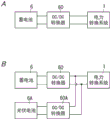
As shown in fig. 1, the power conversion system 1 according to the present embodiment is a system that performs power conversion between a set of dc terminals T11, T12 and a set of ac terminals T21, T22, T23. The battery 6 is configured to be electrically connected to the dc terminals T11 and T12. The power system 7 is configured to be electrically connected to the ac terminals T21, T22, and T23. As used herein, "power system 7" refers to the entire system in which a power provider, such as a power company, supplies power to a power receiving facility of a consumer.
The power conversion system 1 of the present embodiment converts direct-current power input from the battery 6 into alternating-current power having three phases called U-phase, V-phase, and W-phase, and outputs (transmits) the alternating-current power to the power system 7. The power conversion system 1 converts ac power having three phases called U-phase, V-phase, and W-phase, which is input from the power system 7, into dc power, and outputs the dc power to the battery 6. That is, the power conversion system 1 performs power conversion bidirectionally between the set of dc terminals T11, T12 and the set of ac terminals T21, T22, T23.
In other words, to discharge the battery 6, the power conversion system 1 converts the dc power input from the battery 6 into the ac power, and outputs (discharges) the ac power to the power system 7. At this time, the battery 6 functions as a "dc power supply", and the power system 7 functions as a "three-phase ac load" having U-phase, V-phase, and W-phase. In order to charge the battery 6, the power conversion system 1 converts ac power input from the power system 7 into dc power and outputs the dc power to the battery 6 (charges the battery 6 with the dc power). In this state, the battery 6 functions as a "dc load", and the power system 7 functions as a "three-phase ac power supply" having a U-phase, a V-phase, and a W-phase.
The power conversion system 1 of the present embodiment includes a power conversion circuit 2, a buffer circuit 3, a control circuit 4, and a diagnostic unit 5.
The power conversion circuit 2 performs bidirectional power conversion between a set of dc terminals T11 and T12 and a set of ac terminals T21, T22, and T23. The buffer circuit 3 is a protection circuit configured to control ringing or surge voltage generated by the power conversion circuit 2. For example, when the power conversion circuit 2 converts direct-current power into alternating-current power or converts alternating-current power into direct-current power, ringing may occur due to leakage inductance of the transformer 210 included in the power conversion circuit 2. The power conversion system 1 can suppress such ringing through the buffer circuit 3. The diagnosis unit 5 diagnoses the power conversion circuit 2 based on at least one of a voltage of a terminal of the transformer 210, a voltage generated by the snubber circuit 3, or a current generated by the snubber circuit 3.
In the present embodiment, for example, a case where the power storage system including the power conversion system 1 and the battery 6 is introduced into a non-residential facility such as an office building, a hospital, a commercial facility, or a school will be described as an example.
"selling electricity" has become particularly popular recently. By "selling electricity," it is meant the reverse flow of electricity obtained by a juridical or individual from a distributed power source (e.g., photovoltaic cells, battery 6, or fuel cell) to the power system 7. Selling electricity is accomplished by a system interconnect that connects the distributed power sources to the power system 7. In the system interconnection, the power conversion system 1 called a power conditioner is used to convert the electric power of the distributed power source into electric power suitable for the power system 7. The power conversion system 1 according to the present embodiment is used as, for example, a power conditioner, and converts direct-current power into three-phase alternating-current power between the storage battery 6 as a distributed power source and the power system 7, and vice versa.
(2) Structure of the product
The components included in the power conversion system 1 will be described in detail with reference to fig. 1.
(2.1) Power conversion Circuit
The power conversion circuit 2 performs power conversion between the set of two direct current terminals T11 and T12 and the set of three alternating current terminals T21, T22, and T23.
The secondary battery 6, which is a direct-current power source or a direct-current load, is configured to be electrically connected to the direct-current terminals T11 and T12. In the present embodiment, the secondary battery 6 is electrically connected between the dc terminals T11 and T12 such that, of the two dc terminals T11 and T12, the dc terminal T11 has a higher potential (as a positive electrode) and the dc terminal T12 has a lower potential (as a negative electrode).
The power system 7 functioning as a three-phase ac power supply or a three-phase ac load having U, V, and W phases is disposed to be electrically connected to ac terminals T21, T22, and T23. The ac terminal T21 is connected to U, the ac terminal T22 is connected to V, and the ac terminal T23 is connected to W.
The power conversion circuit 2 includes a first conversion circuit 21, a second conversion circuit 22, and a filter circuit 23. The power conversion circuit 2 further includes two direct current terminals T11 and T12 and three alternating current terminals T21, T22, and T23. Note that the two direct current terminals T11 and T12 and the three alternating current terminals T21, T22, and T23 are not necessarily included in the power conversion circuit 2. Further, the "terminal" mentioned here is not necessarily a member for connecting an electric wire or the like, but may be, for example, a lead wire of an electronic component or a part of a conductor included in a circuit board.
The first conversion circuit 21 is, for example, a DC/DC converter. Referring to fig. 1, the first conversion circuit 21 includes a capacitor C10, a transformer 210, and switching elements Q11 to Q14.
The capacitor C10 is electrically connected between the two dc terminals T11 and T12. In other words, the capacitor C10 is connected to the battery 6 through two direct current terminals T11 and T12. The capacitor C10 is, for example, an electrolytic capacitor. The capacitor C10 has a function of stabilizing the voltage between the dc terminals T11 and T12. The capacitor C10 need not be included in the components of the first conversion circuit 21.
Each of the switching elements Q11 to Q14 is, for example, an n-channel depletion type Metal Oxide Semiconductor Field Effect Transistor (MOSFET). Each of the switching elements Q11 to Q14 includes a parasitic diode. The parasitic diodes of the switching elements Q11 to Q14 have anodes electrically connected to the sources of the switching elements Q11 to Q14, respectively, and have cathodes electrically connected to the drains of the switching elements Q11 to Q14, respectively.
Each of the switching elements Q11 to Q14 is controlled by the control circuit 4.
The transformer 210 includes a primary winding wire 211 and a secondary winding wire 212 magnetically connected to each other. The primary winding wire 211 is electrically connected to the capacitor C10 via the switching elements Q11 and Q12. The secondary winding wire 212 is electrically connected to the snubber circuit 3 via the switching elements Q13 and Q14.
The transformer 210 is, for example, a high-frequency insulation transformer equipped with a center tap. The primary winding wire 211 of the transformer 210 includes a series circuit of two winding wires L11 and L12 with the primary side center tap CT1 as a connection point. Similarly, the secondary winding wire 212 of the transformer 210 includes a series circuit of two winding wires L13 and L14 with the secondary-side center tap CT2 as a connection point. That is, the two winding wires L11 and L12 are electrically connected in series with each other to form the primary winding wire 211. Similarly, the two winding wires L13 and L14 are electrically connected in series with each other to form the secondary winding wire 212. The primary side center tap CT1 is electrically connected to the terminal of the positive side (the direct current terminal T11 side) of the capacitor C10. The secondary-side center tap CT2 is electrically connected to a terminal T31 described later. The turn ratio of the winding wires L11, L12, L13 and L14 is, for example, 1: 1. The turn ratios of the winding wires L11, L12, L13, and L14 may be arbitrarily changed according to the specification and the like of the power conversion system 1.
The voltage between both ends of the battery 6 is applied as an input voltage Vi to the first conversion circuit 21 via the dc terminals T11 and T12.
In the first conversion circuit 21, the on/off of the switching elements Q11 and Q12 converts the input voltage Vi into a rectangular-wave high-frequency alternating-current voltage of, for example, 20kHz, and applies the rectangular-wave high-frequency alternating-current voltage to the primary winding wire 211 (winding wires L11 and L12).
The switching element Q11 is electrically connected in series with the winding wire L11 between both ends of the capacitor C10. The switching element Q12 is electrically connected in series with the winding wire L12 between both ends of the capacitor C10. In other words, between the dc terminals T11 and T12, the series circuit of the switching element Q11 and the winding wire L11 is electrically connected in parallel with the series circuit of the switching element Q12 and the winding wire L12.
The drain of the switching element Q11 is electrically connected to the primary side center tap CT1 via the winding wire L11. The drain of the switching element Q12 is electrically connected to the primary side center tap CT1 via the winding wire L12. The sources of the switching elements Q11 and Q12 are electrically connected to a low potential (negative) side dc terminal T12.
In the first conversion circuit 21, the switching elements Q13 and Q14 are turned on/off to convert a rectangular wave alternating-current voltage having positive and negative polarities generated at the secondary winding wire 212 (the winding wires L13 and L14) into a direct-current voltage having a positive polarity, and output the direct-current voltage between the two terminals T31 and T32. In the present embodiment, a voltage is supplied between the terminals T31 and T32, so that of the two terminals T31 and T32, the terminal T31 has a higher potential (as a positive electrode) and the terminal T32 has a lower potential (as a negative electrode).
The switching element Q13 is electrically connected in series with the winding wire L13 between the terminals T31, T32. The switching element Q14 is electrically connected in series with the winding wire L14 between the terminals T31, T32. That is, between the terminals T31 and T32, the series circuit of the switching element Q13 and the winding wire L13 is electrically connected in parallel with the series circuit of the switching element Q14 and the winding wire L14.
The drain of the switching element Q13 is electrically connected to the secondary side center tap CT2 via the winding wire L13. The drain of the switching element Q14 is electrically connected to the secondary side center tap CT2 via the winding wire L14. The sources of the switching elements Q13 and Q14 are electrically connected to a low potential (negative) side terminal T32.
The second converter circuit 22 is a three-phase inverter circuit that converts a dc voltage between terminals T31 and T32 into a rectangular wave ac voltage, and includes 6 bridge-connected switching elements Q21 to Q26.
Each of the switching elements Q21 to Q26 is, for example, an n-channel depletion type MOSFET. The high-side switching device Q21 is electrically connected in series to the low-side switching device Q22 between the terminals T31 and T32. The high-side switching device Q23 is electrically connected in series to the low-side switching device Q24 between the terminals T31 and T32. The high-side switching device Q25 is electrically connected in series to the low-side switching device Q26 between the terminals T31 and T32.
The drains of the high-side switching elements Q21, Q23, and Q25 are electrically connected to the terminal T31. The sources of the low-potential-side switching elements Q22, Q24, and Q26 are electrically connected to a terminal T32. The source of the high-side switching element Q21 is electrically connected to the drain of the low-side switching element Q22. The source of the high-side switching element Q23 is electrically connected to the drain of the low-side switching element Q24. The source of the high-side switching element Q25 is electrically connected to the drain of the low-side switching element Q26.
That is, the series circuit of the switching elements Q21 and Q22, the series circuit of the switching elements Q23 and Q24, and the series circuit of the switching elements Q25 and Q26 are electrically connected in parallel to each other between the terminals T31 and T32. The series circuit of the switching elements Q21 and Q22 forms a U-phase circuit corresponding to U. The series circuit of the switching elements Q23 and Q24 forms a V-phase circuit corresponding to V. The series circuit of the switching elements Q25 and Q26 forms a W-phase circuit corresponding to W.
Each of the switching elements Q21 to Q26 includes a parasitic diode. The parasitic diodes of the switching elements Q21 to Q26 have anodes electrically connected to the sources of the switching elements Q21 to Q26, respectively, and have cathodes electrically connected to the drains of the switching elements Q21 to Q26, respectively.
Each of the switching elements Q21 to Q26 is controlled by the control circuit 4.
The filter circuit 23 smoothes the rectangular wave ac voltage output from the second converter circuit 22. Therefore, the rectangular wave alternating-current voltage output from the second conversion circuit 22 is converted into a sine wave alternating-current voltage having an amplitude according to the pulse width.
Specifically, the filter circuit 23 includes a plurality of (three in fig. 1) inductors L21, L22, and L23 and a plurality of (three in fig. 1) capacitors C21, C22, and C23. One end of the inductor L21 is electrically connected to a connection point between the switching elements Q21 and Q22. The other end of the inductor L21 is electrically connected to the ac terminal T21. One end of the inductor L22 is electrically connected to a connection point between the switching elements Q23 and Q24. The other end of the inductor L22 is electrically connected to the ac terminal T22. One end of the inductor L23 is electrically connected to a connection point between the switching elements Q25 and Q26. The other end of the inductor L23 is electrically connected to the ac terminal T23. The capacitor C21 is electrically connected between the ac terminals T21 and T22. The capacitor C22 is electrically connected between the ac terminals T22 and T23. The capacitor C23 is electrically connected between the ac terminals T21 and T23.
That is, a connection point between the switching elements Q21, Q22 constituting the U-phase circuit is electrically connected to the ac terminal T21 corresponding to U via the inductor L21. A connection point between the switching elements Q23, Q24 constituting the V-phase circuit is electrically connected to an ac terminal T22 corresponding to V via an inductor L22. A connection point between the switching elements Q25, Q26 constituting the W-phase circuit is electrically connected to an ac terminal T23 corresponding to W via an inductor L23.
(2.2) buffer Circuit
The snubber circuit 3 is electrically connected to the terminals T31 and T32 in the power conversion circuit 2. That is, the snubber circuit 3 is electrically connected to the transformer 210 through the terminals T31 and T32.
The buffer circuit 3 is a regenerative buffer circuit configured to extract electric energy from the power conversion circuit 2 and inject (regenerate) the electric energy into the power conversion circuit 2. When the bus voltage Vbus between the terminals T31 and T32 exceeds the first clamp value, the buffer circuit 3 extracts electric energy exceeding the first clamp value from the power conversion circuit 2, thereby clamping the upper limit value of the bus voltage Vbus at the first clamp value. Further, when the bus voltage Vbus is smaller than the second clamp value (second clamp value < first clamp value), the buffer circuit 3 injects (regenerates) electric energy to the power conversion circuit 2, thereby clamping the lower limit value of the bus voltage Vbus at the second clamp value.
The buffer circuit 3 includes a first clamping circuit 31, a second clamping circuit 32, and a voltage conversion circuit 33.
The first clamp circuit 31 is a circuit configured to extract electric energy from the power conversion circuit 2 when the bus voltage Vbus exceeds a first clamp value. The first clamping circuit 31 includes a diode D31 and a capacitor C31. The diode D31 and the capacitor C31 are electrically connected in series with each other between the terminals T31 and T32. The first clamp circuit 31 is configured to allow a current to flow from the power conversion circuit 2 to the capacitor via the diode D31 when the bus voltage Vbus exceeds the first clamp value. Specifically, the diode has an anode electrically connected to the terminal T31 on the high potential side and a cathode electrically connected to the terminal T32 on the low potential side via the capacitor C31.
In the first clamp circuit 31, assuming that the magnitude of the voltage across the capacitor C31 (also referred to as the first clamp voltage V31) is the first clamp value, in this case, when the bus voltage Vbus exceeds the first clamp value, the diode D31 is turned on, so that a current flows through the capacitor C31. Strictly speaking, the first clamp voltage is a voltage obtained by adding the forward voltage drop of the diode D31 to the voltage across the capacitor C31 (the first clamp voltage V31). Note that the forward voltage drop of the diode D31 is much smaller than the first clamping value, and therefore, the present embodiment is described with the forward voltage drop of the diode D31 being zero, i.e., the magnitude of the voltage across the capacitor C31 (the first clamping voltage V31) corresponds to the first clamping value.
The second clamp circuit 32 is a circuit configured to inject (regenerate) electric energy to the power conversion circuit 2 when the bus voltage Vbus is smaller than the second clamp value. The second clamping circuit 32 includes a diode D32 and a capacitor C32. The diode D32 and the capacitor C32 are electrically connected in series with each other between the terminals T31 and T32. The second clamp circuit 32 is configured to allow current to flow from the capacitor C32 to the power conversion circuit 2 via the diode D32 when the bus voltage Vbus is less than the second clamp value. Specifically, the diode D32 has a cathode electrically connected to the terminal T31 on the high potential side, and an anode electrically connected to the terminal T32 on the low potential side via the capacitor C32.
In the second clamp circuit 32, assuming that the magnitude of the voltage across the capacitor C32 (also referred to as a second clamp voltage V32) is a second clamp value, in this case, when the bus voltage Vbus is smaller than the second clamp value, the diode D32 is turned on, so that a current flows through the power conversion circuit 2. Strictly speaking, the second clamp value is a voltage obtained by adding the forward voltage drop of the diode D32 to the voltage across the capacitor C32 (second clamp voltage V32). Note that the forward voltage drop of the diode D32 is much smaller than the second clamping value, and therefore, the present embodiment is described with the forward voltage drop of the diode D32 being zero, i.e., the magnitude of the voltage across the capacitor C32 (the second clamping voltage V32) corresponds to the second clamping value.
The voltage conversion circuit 33 is electrically connected to the first clamping circuit 31 and the second clamping circuit 32. The voltage conversion circuit 33 performs voltage conversion (step-down, step-up, or step-down) between the first clamping voltage V31 and the second clamping voltage V32
The voltage conversion circuit 33 is a chopper-type DC/DC converter including switching elements Q31 and Q32 and an inductor L31. In the present embodiment, the voltage conversion circuit 33 is a step-down chopper circuit that steps down the first clamped voltage V31 to generate the second clamped voltage V32. The switching elements Q31 and Q32 are both n-channel depletion MOSFETs.
The switching elements Q31 and Q32 are electrically connected in series between both ends of the capacitor C31. The drain of the switching element Q31 is electrically connected to the cathode of the diode D31. The source of the switching element Q32 is electrically connected to the negative electrode-side terminal (terminal T32) of the capacitor C31.
The inductor L31 is electrically connected to the switching element Q32 between both ends of the capacitor C32. Specifically, the inductor L31 is electrically connected between the connection point of the source of the switching element Q31 and the drain of the switching element Q32 and the connection point of the anode of the diode D32 and the capacitor C32.
(2.3) control Circuit
The control circuit 4 includes a microcomputer having a processor and a memory. That is, the control circuit 4 is implemented by a computer system including a processor and a memory. The processor executes an appropriate program, thereby causing the computer system to function as the control circuit 4. The program may be stored in the memory in advance, may be provided via a telecommunication network such as the internet, or may be provided via a non-transitory storage medium such as a memory card storing the program.
The control circuit 4 is configured to control the first and second conversion circuits 21 and 22 of the power conversion circuit 2 and the voltage conversion circuit 33 of the buffer circuit 3. The control circuit 4 outputs drive signals S11 to S14 for driving the switching elements Q11 to Q14, respectively, to the first conversion circuit 21. The control circuit 4 outputs drive signals S21 to S26 for driving the switching elements Q21 to Q26, respectively, to the second conversion circuit 22. The control circuit 4 outputs drive signals S31, S32 for driving the switching elements Q31, Q32, respectively, to the voltage conversion circuit 33. Each of the drive signals S11 to S14, S21 to S26, and S31 and S32 is a PWM signal including a binary signal that is switchable between a high level (an example of an active value) and a low level (an example of an inactive value).
(2.4) diagnostic Unit
The diagnostic unit 5 comprises a microcomputer with a processor and a memory. That is, the diagnosis unit 5 is implemented by a computer system including a processor and a memory. The processor executes a suitable program, thereby causing the computer system to function as the diagnostic unit 5. The program may be stored in the memory in advance, may be provided via a telecommunication network such as the internet, or may be provided via a non-transitory storage medium such as a memory card storing the program.
The diagnosis unit 5 is configured to perform diagnosis of the power conversion circuit 2. Here, "diagnosis of the power conversion circuit 2" refers to determining whether there is an abnormality in the power conversion circuit 2.
In the present embodiment, when an abnormality occurs in the power conversion circuit 2, the voltage of the terminal of the transformer 210 changes. Examples of the abnormality in the power conversion circuit 2 include an increase in leakage inductance of the transformer 210, an increase in excitation inductance due to magnetic biasing of the transformer 210, an increase or decrease in parasitic capacitance of the first conversion circuit 21, and a change in threshold voltage of the switching elements (Q11 to Q14). When such an abnormality exists in the power conversion circuit 2, the voltage of the terminal of the transformer 210 rises. Examples of the voltage of the terminal of the transformer 210 include, for example, the voltage VT2 across the secondary winding wire 212 of the transformer 210, the voltage across the winding wire L13, and the voltage across the winding wire L14.
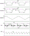
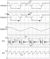
Fig. 2 shows an operation waveform diagram when the power conversion circuit 2 is in a normal state. Further, fig. 3 shows an operation waveform diagram in the case where the power conversion circuit 2 is in an abnormal state, specifically, in the case where the leakage inductance of the transformer 210 is increased as compared with the normal state. In addition, fig. 4 shows an operation waveform diagram in the case where the power conversion circuit 2 is in another abnormal state, specifically, in the case where the excitation inductance of the transformer 210 is increased as compared with the normal state. In fig. 2 to 4, the uppermost shows graphs of the voltage VT1 across the primary winding wire 211 of the transformer 210 and the input current IT1 to the primary-side center-tap CT 1; the second section shows a graph of the voltage VT2 across the secondary winding wire 212 of the transformer 210 and the output current IT2 from the secondary side center-tap CT 2; the third section shows a graph of the excitation current of the transformer 210; the fourth section shows a graph of the bus voltage Vbus between the terminals T31, T32, the first clamping voltage V31 and the second clamping voltage V32 of the buffer circuit 3; the fifth section shows a graph of the internal current I31 flowing through the inductor L31 in the buffer circuit 3.
Referring to fig. 2 and 3, in an abnormal state in which the leakage inductance of the transformer 210 increases, the ringing of the voltage VT2 across the secondary winding wire 212 of the transformer 210 increases as compared to a normal state. Therefore, in the case where the power conversion circuit 2 is normal, the peak value of the voltage VT2 across the secondary winding wire 212 of the transformer 210 is v11, and in the case where the power conversion circuit 2 is abnormal, the peak value of the voltage VT2 across the secondary winding wire 212 of the transformer 210 is v12 which is greater than v 11. The increased ringing of the voltage VT2 between the two ends of the secondary winding wire 212 increases the electric energy extracted from the power conversion circuit 2 by the snubber circuit 3. As a result, when the power conversion circuit 2 is in the abnormal state, the value and the effective value of the voltage across the capacitor C31 (first clamp voltage V31) in the first clamp circuit 31 of the snubber circuit 3 increase as compared to the case where the power conversion circuit 2 is in the normal state. In fig. 2 and 3, in the case where the power conversion circuit 2 is in the normal state, the peak value of the first clamp voltage V31 is V21, and in the case where the power conversion circuit 2 is in the abnormal state, the peak value of the first clamp voltage V31 is increased to V22 which is greater than V21. Further, when the power conversion circuit 2 is in the abnormal state, the electric energy transmitted from the first clamp circuit 31 to the second clamp circuit 32 (i.e., the value and effective value of the internal current I31 flowing through the inductor L31) is increased as compared with the case where the power conversion circuit 2 is in the normal state. In fig. 2 and 3, in the case where the power conversion circuit 2 is in the normal state, the peak value of the internal current I31 is I31, and in the case where the power conversion circuit 2 is in the abnormal state, the peak value of the internal current I31 is increased to I32 larger than I31.
In addition, as shown in fig. 2 and 4, in an abnormal state in which the excitation inductance of the transformer 210 increases, the excitation current becomes smaller than in a normal state. In fig. 2 and 4, in the case where the power conversion circuit 2 is in the normal state, the peak value of the excitation current is i41, and in the case where the power conversion circuit 2 is in the abnormal state, the peak value of the excitation current is reduced to i42 which is smaller than i 41. In the first conversion circuit 21, the leakage inductance and the resonance of the excitation inductance and the parasitic capacitance of the transformer 210 realize soft switching of the switching elements Q11 to Q14. However, if an increase in the excitation inductance (a decrease in the excitation current) changes the resonance frequency, soft switching cannot be achieved, and the switching operation of the switching elements Q11 to Q14 results in hard switching. Therefore, the peak value of the voltage VT2 across the secondary winding wire 212 of the transformer 210 in the case where the power conversion circuit 2 is normal is v11, and the peak value of the voltage VT2 across the secondary winding wire 212 of the transformer 210 in the case where the power conversion circuit 2 is abnormal is v13 which is greater than v 11. The increased ringing of the voltage VT2 between the two ends of the secondary winding wire 212 increases the electric energy extracted from the power conversion circuit 2 by the snubber circuit 3. As a result, when the power conversion circuit 2 is in the abnormal state, the value and the effective value of the voltage across the capacitor C31 (first clamp voltage V31) in the first clamp circuit 31 of the snubber circuit 3 increase as compared to the case where the power conversion circuit 2 is in the normal state. In fig. 2 and 4, the peak value of the first clamp voltage V31 in the normal state of the power conversion circuit 2 is V21, and the peak value of the first clamp voltage V31 in the abnormal state of the power conversion circuit 2 increases to V23 larger than V21. Further, when the power conversion circuit 2 is in the abnormal state, the electric energy transmitted from the first clamp circuit 31 to the second clamp circuit 32 (i.e., the value and effective value of the internal current I31 flowing through the inductor L31) is increased as compared with the case where the power conversion circuit 2 is in the normal state. In fig. 2 and 4, the peak value of the internal current I31 of the power conversion circuit 2 in the normal state is I31, and the peak value of the internal current I31 of the power conversion circuit 2 in the abnormal state is increased to I33 larger than I31.
Therefore, when the power conversion circuit 2 is in the abnormal state, the voltage of the terminals of the transformer 210 (i.e., the voltage VT2 between the two ends of the secondary winding wire 212) and the bus voltage Vbus both increase as compared to the case where the power conversion circuit 2 is in the normal state. As the bus voltage Vbus increases, the power extracted and regenerated by the buffer circuit 3 increases. As a result, the voltage and current generated by the buffer circuit 3 increase. Examples of the voltage generated by the buffer circuit 3 include a voltage across the capacitor C31 (first clamping voltage V31) and a voltage across the capacitor C32 (second clamping voltage V32). Examples of the current generated by the buffer circuit 3 include an internal current I31 flowing through the inductor L31, an input current flowing through the diode D31, and an output current flowing through the diode D32.
In the present embodiment, the diagnosing unit 5 diagnoses the power conversion circuit 2 based on the main information, which is at least one of the voltage of the terminal of the transformer 210, the voltage generated by the snubber circuit 3, or the current generated by the snubber circuit 3. In addition to the main information, the diagnosis unit 5 diagnoses the power conversion circuit 2 based on the auxiliary information.
The main information includes information on at least any one of the voltage of the terminal of the transformer 210, the voltage generated by the snubber circuit 3, or the current generated by the snubber circuit 3. Examples of the voltage of the terminal of the transformer 210 include, for example, the voltage VT2 across the secondary winding wire 212 of the transformer 210, the voltage across the winding wire L13, and the voltage across the winding wire L14. Examples of the voltage generated by the buffer circuit 3 include a voltage across the capacitor C31 (first clamping voltage V31) and a voltage across the capacitor C32 (second clamping voltage V32). Examples of the current generated by the buffer circuit 3 include an internal current I31 flowing through the inductor L31, an input current flowing through the diode D31, and an output current flowing through the diode D32. In the present embodiment, the diagnostic unit 5 uses the current generated by the buffer circuit 3 (specifically, the internal current I31 flowing through the inductor L31) as main information. The diagnostic unit 5 obtains a sensing result of the internal current I31 from a current detector provided in the power conversion circuit 2 as main information.
The auxiliary information includes information on at least any one of the input power, the output power, or the temperature of the power conversion circuit 2. The input power of the power conversion circuit 2 includes not only the input power value or the input power amount input from the battery 6 to the power conversion circuit 2 but also an input voltage Vi that is a voltage across the battery 6 and an input current Ii supplied from the battery 6 to the power conversion circuit 2. The output power of the power conversion circuit 2 includes not only the output power value or the output power amount output from the power conversion circuit 2 to the power system 7, but also the output voltage Vo and the output current Io. The output voltage Vo may be a voltage between any two of the three ac terminals T21, T22, and T23, may be a voltage between the terminals, may be an average value of the voltages between the terminals, or the like. The output current Io may be a current flowing through any one of the three ac terminals T21, T22, and T23, may be a current flowing through each terminal, may be an average value of currents flowing through each terminal, or the like. The temperature of the power conversion circuit 2 is, for example, the temperature of at least any one of the switching elements Q11 to Q14 and Q21 to Q26 or the temperature of the transformer 210. Further, the auxiliary information may include a temperature of the buffer circuit 3, specifically, a temperature of at least one of the switching elements Q31 or Q32. In the present embodiment, the diagnosis unit 5 uses the output power and the input power (specifically, the output current Io and the input voltage Vi) as the auxiliary information. The diagnosis unit 5 obtains sensing results of the output current Io and the input voltage Vi as auxiliary information from a current detector and a voltage detector provided in the power conversion circuit 2, respectively.
The diagnosis unit 5 sets a determination range (normal range, abnormal range, attention range) to be compared with the value of the internal current I31 flowing through the inductor L31 as the main information, based on the auxiliary information thus obtained.
The normal range is a range that the value of the main information (the internal current I31 flowing through the inductor L31) can take when the state of the power conversion circuit 2 is the normal state. If the value of the internal current I31 is included in the normal range, the diagnostic unit 5 determines that the power conversion circuit 2 is in the normal state.
The abnormal range is a range that can be taken by the value of the main information (the internal current I31 flowing through the inductor L31) when the state of the power conversion circuit 2 is the abnormal state, and the abnormal range is a range outside the normal range. If the value of the internal current I31 is contained in the abnormal range, the diagnostic unit 5 determines that the power conversion circuit 2 is in the abnormal state.
The attention range is a range that the value of the main information (the internal current I31 flowing through the inductor L31) can take when the state of the power conversion circuit 2 is the attention state, and the attention range is a range between the normal range and the abnormal range. Note that the state is a state close to the abnormal state in which the state of the power conversion circuit 2 is not currently the abnormal state but is highly likely to transition to the abnormal state. If the value of the internal current I31 is included in the attention range, the diagnostic unit 5 determines that the power conversion circuit 2 is in the attention state.
In the present embodiment, the diagnosis unit 5 sets the above-described determination ranges (normal range, abnormal range, and attention range) according to the magnitudes of the output current Io and the input voltage Vi as the auxiliary information. Fig. 5 is a graph showing an example of the determination range. In fig. 5, the output current Io is plotted along the abscissa, and the internal current I31 is plotted along the ordinate.
In fig. 5, Z11 represents the upper limit value of the normal range (the lower limit value of the attention range) when the input voltage Vi is the lower limit value, and Z12 represents the lower limit value of the abnormal range (the upper limit value of the attention range) when the input voltage Vi is the lower limit value. In the case where the input voltage Vi is the lower limit value, the normal range is a range less than or equal to the upper limit value Z11 of the normal range, note that the range is a range between the upper limit value Z11 of the normal range and the lower limit value Z12 of the abnormal range, and the abnormal range is a range greater than or equal to the lower limit value Z12 of the abnormal range. Z21 represents the upper limit value of the normal range (the lower limit value of the attention range) when the input voltage Vi is the upper limit value, and Z22 represents the lower limit value of the abnormal range (the upper limit value of the attention range) when the input voltage Vi is the upper limit value. In the case where the input voltage Vi is the upper limit value, the normal range is a range less than or equal to the upper limit value Z21 of the normal range, note that the range is a range between the upper limit value Z21 of the normal range and the lower limit value Z22 of the abnormal range, and the abnormal range is a range greater than or equal to the lower limit value Z22 of the abnormal range.
As shown in fig. 5, the diagnosis unit 5 sets a determination range according to the magnitudes of the output current Io and the input voltage Vi. For example, assume that the side information represents a value of: the value of the input voltage Vi is a lower limit value, and the value of the output current Io is X1. In this case, the diagnostic unit 5 sets the upper limit value to the normal range of Y11. The diagnostic unit 5 sets the attention range with a lower limit value of Y11 and an upper limit value of Y12. The diagnostic unit 5 sets the lower limit value to the abnormality range of Y12. Assume that the value of the internal current I31 represented by the main information is Y1, which is greater than Y12. In this case, the value Y1 of the internal current I31 is included in the abnormal range, and the diagnostic unit 5 determines that the power conversion circuit 2 is in the abnormal state.
In addition, for example, assume that the auxiliary information indicates a value of: the value of the input voltage Vi is an upper limit value, and the value of the output current Io is X1. In this case, the diagnostic unit 5 sets the upper limit value to the normal range of Y21. The diagnostic unit 5 sets the attention range with a lower limit value of Y21 and an upper limit value of Y22. The diagnostic unit 5 sets the lower limit value to the abnormality range of Y22. Assume that the value of the internal current I31 represented by the main information is Y1, which is smaller than Y21. In this case, the value Y1 of the internal current I31 is included in the normal range, and the diagnostic unit 5 determines that the power conversion circuit 2 is in the normal state.
That is, the diagnosing unit 5 diagnoses the power conversion circuit 2 in consideration of the operating condition of the power conversion circuit 2, and therefore, the diagnosis accuracy can be improved, and errors can be reduced.
Further, in the present embodiment, the diagnostic unit 5 uses the internal current I31 flowing through the inductor L31 of the buffer circuit 3 as main information.
As described above, ringing of the voltage VT2 across the secondary winding wire 212 of the transformer 210 increases in the case where there is an abnormality in the power conversion circuit 2 as compared with the case of the normal state, thereby instantaneously increasing the peak value (see fig. 2 and 4). Therefore, when the peak of the voltage VT2 is used as the value of the main information, the peak of the voltage VT2 must be detected by a voltage detector having a higher time resolution. In contrast, in the case of using the internal current I31 as the value of the main information, current peaks are repeatedly generated, so that a current detector with a lower time resolution can be used, and the peak value of the internal current I31 is easier to measure than the peak value of the voltage VT 2. Therefore, the diagnostic accuracy of the power conversion circuit 2 can be improved.
Further, as described above, in the case where there is an abnormality in the power conversion circuit 2, the first clamp voltage V31 across the capacitor C31 of the snubber circuit 3 increases (see fig. 2 to 4) as compared with the case of the normal state. However, the difference between the first clamping voltage V31 in the case where the power conversion circuit 2 is in the normal state and the first clamping voltage V31 in the case where the power conversion circuit 2 is in the abnormal state is relatively small. Therefore, when the peak value of the first clamping voltage V31 is used as the value of the main information, the peak value of the first clamping voltage V31 must be detected by a voltage detector having higher voltage resolution. In contrast, in the case where the internal current I31 is used as the value of the main information, the difference between the internal current I31 in the normal state of the power conversion circuit 2 and the internal current I31 in the abnormal state of the power conversion circuit 2 is larger than the first clamp voltage V31. Therefore, the determination process of determining in which of the normal range, the abnormal range, and the attention range the value of the internal current I31 is included becomes easy, and the diagnosis accuracy of the power conversion circuit 2 can be improved.
The power conversion system 1 of the present embodiment further includes an outputter 51.
The output unit 51 is configured to output a diagnosis result of the diagnosis unit 5. The outputter 51 is, for example, a communication interface and is configured to communicate with the server 8 based on an appropriate communication scheme of wired communication or wireless communication. In the present embodiment, the outputter 51 is configured to communicate with the server 8 through a public network 80 such as the internet.
The output unit 51 receives the diagnosis result from the diagnosis unit 5, and outputs the received diagnosis result to the server 8 (external system). In other words, the diagnosis unit 5 outputs the diagnosis result to the server 8 through the outputter 51.
Thus, for example, an administrator of the power conversion system 1 can manage the state of the power conversion circuit 2.
The diagnosis unit 5 (outputter 51) may periodically output the diagnosis result to the server 8 regardless of the content of the diagnosis result. Alternatively, the diagnosing unit 5 (outputter 51) may output a notification signal to the server 8 as a diagnosis result for notifying the state of the power conversion circuit when the power conversion circuit 2 is in the attentive state or the abnormal state.
Note that the outputter 51 may output the diagnosis result to an external system (e.g., a server) provided in the same facility as the power conversion system 1. In this case, the outputter 51 outputs the diagnosis result to an external system via a local network provided in the facility.
(3) Example of operation
(3.1) operation of Power conversion Circuit
Referring to fig. 1, the operation of the power conversion circuit 2 will be briefly described below.
In the present embodiment, as described above, the power conversion circuit 2 is configured to perform bidirectional power conversion via the transformer 210 between the two primary-side terminals T11 and T12 of one set and the three alternating-current terminals T21, T22, and T23 of one set. That is, the power conversion circuit 2 has two operation modes, i.e., "inverter mode" and "converter mode". The inverter mode is an operation mode in which direct-current power input to the two direct-current terminals T11 and T12 is converted into three-phase alternating-current power, and the three-phase alternating-current power is output from the three alternating-current terminals T21, T22, and T23. The converter mode is an operation mode in which three-phase alternating-current power input to the three alternating-current terminals T21, T22, and T23 is converted into direct-current power, and the direct-current power is output from the two direct-current terminals T11 and T12.
In other words, the inverter mode refers to a mode in which: between the three alternating-current terminals T31, T32, T33, a pattern of voltage drop, that is, a pattern of voltage and current of the same polarity is generated in the same direction as the direction in which the current flows through the power system 7. The converter mode is a mode in which: between the three alternating-current terminals T21, T22, and T23, a pattern of voltage drop is generated in a direction different from the direction in which current flows through the power system 7, that is, a pattern of voltage and current of different polarities is generated.
In the present embodiment, the following example will be described: the operation mode of the power conversion circuit 2 is an inverter mode, and the power conversion circuit 2 converts direct-current power into three-phase alternating-current power having a frequency of 50Hz or 60 Hz. For example, the driving frequency of each of the switching elements Q11 to Q14 is 20 kHz.
The control circuit 4 controls the switching elements Q11 and Q12 such that positive and negative voltages are alternately applied to the primary winding wire 211. Further, the control circuit 4 controls the switching elements Q13 and Q14 such that the voltage of the terminal T31 is positive with respect to the voltage of the terminal T32.
Specifically, the control circuit 4 turns off the switching elements Q12 and Q14 when the switching elements Q11 and Q13 are turned on, and the control circuit 4 turns on the switching elements Q12 and Q14 when the switching elements Q11 and Q13 are turned off. In the present embodiment, the control circuit 4 controls the switching elements Q11 to Q14 at the same duty ratio. In the present embodiment, the duty ratio of each of the switching elements Q11 to Q14 is "0.5" (substantially 50%).
In the present embodiment, the control circuit 4 controls the switching elements Q11 and Q12 such that the high-frequency alternating-current voltage is supplied to the primary winding wire 211 and the secondary winding wire 212, and the control circuit 4 controls the switching elements Q13 and Q14 such that the voltage having the positive polarity is supplied to the terminals T31 and T32.
Further, the control circuit 4 controls the magnitude of at least one of the voltages or currents output from the alternating-current terminals T21, T22, and T23 by turning on or off each of the switching elements Q21 to Q26.
In the present embodiment, the control circuit 4 controls the second conversion circuit 22 such that electric power is not transmitted between the first conversion circuit 21 and the second conversion circuit 22 in the first period including the inversion period in which the polarity of the voltage applied to the primary winding wire 211 is inverted. Further, the control circuit 4 controls the second conversion circuit 22 so that power is transmitted in a first direction from the first conversion circuit 21 to the second conversion circuit 22 or a second direction opposite to the first direction in a second period different from the first period.
Specifically, the control circuit 4 operates to repeat the first to fourth modes described below.
In the first mode, the control circuit 4 outputs the drive signals S11 to S14 so that the switching elements Q11 and Q13 are turned on and the switching elements Q12 and Q14 are turned off. Therefore, the voltage across the winding wire L11 of the primary winding wire 211 is "+ Vi". Further, the voltage across the winding wire L13 of the secondary winding wire 212 is therefore "+ Vi". At this time, the switching element Q13 is turned on, and thus the bus voltage Vbus between the terminals T31 and T32 is "+ Vi".
In the second mode, the control circuit 4 outputs the drive signals S21 to S26 so that the switching elements Q22, Q24, and Q26 on the low potential side are turned off and the switching elements Q21, Q23, and Q25 on the high potential side are turned on. This realizes a circulation mode in which current circulates in the second conversion circuit 22. At this time, all of the switching elements Q11 to Q14 of the first conversion circuit 21 are turned off.
In the third mode, the control circuit 4 outputs the drive signals S11 to S14 so that the switching elements Q12 and Q14 are turned on and the switching elements Q11 and Q13 are turned off. Therefore, the voltage across the winding wire L12 of the primary winding wire 211 is "-Vi". In addition, the voltage across the winding wire L14 of the secondary winding wire 212 is therefore "-Vi". At this time, the switching element Q14 is turned on, and thus the bus voltage Vbus between the terminals T31 and T32 is "+ Vi".
In the fourth mode, the control circuit 4 outputs the drive signals S21 to S26 so that the high-side switching elements Q21, Q23, and Q25 are turned off and the low-side switching elements Q22, Q24, and Q26 are turned on. This realizes a circulation mode in which current circulates in the second conversion circuit 22. At this time, all of the switching elements Q11 to Q14 of the first conversion circuit 21 are turned off.
The control circuit 4 repeats the operation in the order of the first mode, the second mode, the third mode, and the fourth mode. In this way, the power conversion circuit 2 converts the direct-current power from the battery 6 into three-phase alternating-current power, and outputs the three-phase alternating-current power to the power system 7 from the three alternating-current terminals T21, T22, and T23.
(3.2) operation of buffer circuits
Referring to fig. 1, the operation of the buffer circuit 3 will be briefly described below.
When positive ringing occurs in the bus voltage Vbus, the buffer circuit 3 extracts the power of the power conversion circuit 2 through the first clamp circuit 31, clamping the bus voltage Vbus at a first clamp value (see fig. 2). In the first clamp circuit 31, the magnitude of the voltage across the capacitor C31 (first clamp voltage V31) is a first clamp value.
That is, when the bus voltage Vbus is subjected to positive ringing, which causes the magnitude of the bus voltage Vbus to exceed the first clamp value, the diode D31 is turned on, and the first clamp circuit 31 operates. At this time, as the first clamp circuit 31 draws electric power, a current having a pulse shape flows through the diode D31. This enables the buffer circuit 3 to extract the electric energy corresponding to the electric energy exceeding the first clamp value from the power conversion circuit 2 and store the electric energy in the capacitor C31 when the magnitude of the bus voltage Vbus exceeds the first clamp value. Therefore, even when positive ringing occurs in the bus voltage Vbus, the maximum value of the bus voltage Vbus is suppressed to the first clamp value.
Further, the buffer circuit 3 performs voltage conversion between the first clamping voltage V31 and the second clamping voltage V32 by a voltage conversion circuit 33 electrically connected between the first clamping circuit 31 and the second clamping circuit 32. The voltage conversion circuit 33 alternately turns on the switching elements Q31 and Q32 to lower the first clamping voltage V31 based on the driving signals S31 and S32 from the control circuit 4, thereby generating the second clamping voltage V32. Therefore, the value of the voltage across the capacitor C32 as the second clamping voltage V32 (second clamping value) is smaller than the value of the voltage across the capacitor C31 as the first clamping voltage V31 (first clamping value). To sum up, when the first clamp circuit 31 operates and accumulates electric energy in the capacitor C31, at least a part of the electric energy is transferred to the capacitor C32 of the second clamp circuit 32 through the voltage conversion circuit 33 and accumulated in the capacitor C32.
Also, when the bus voltage Vbus exhibits negative ringing, the buffer circuit 3 injects (regenerates) electric energy to the power conversion circuit 2 through the second clamp circuit 32, thereby clamping the bus voltage Vbus at the second clamp value (see fig. 2). In the second clamp circuit 32, the magnitude of the voltage across the capacitor C32 (second clamp voltage V32) is a second clamp value.
That is, when the bus voltage Vbus undergoes negative ringing, which causes the magnitude of the bus voltage Vbus to be lower than the second clamping value, the diode D32 is turned on, and the second clamping circuit 32 operates. At this time, as the second clamp circuit 32 injects (regenerates) the electric power, a current having a pulse shape flows through the diode D32. Therefore, when the magnitude of the bus voltage Vbus is lower than the second clamp value, the buffer circuit 3 causes the electric energy corresponding to the current lower than the second clamp value to be regenerated from the capacitor C32 to the power conversion circuit 2. Therefore, even in the case where negative ringing occurs in the bus voltage Vbus, the minimum value of the bus voltage Vbus is suppressed to the second clamp value.
In the present embodiment, as described above, the electric energy stored in the capacitor C32 is the electric energy sent from the capacitor C31 via the voltage conversion circuit 33. That is, the buffer circuit 3 regenerates the electric energy extracted from the power conversion circuit 2 by the first clamp circuit 31 when the bus voltage Vbus is subjected to positive ringing, from the second clamp circuit 32 to the power conversion circuit 2 when the bus voltage Vbus is subjected to negative ringing. In other words, in the buffer circuit 3, the electric energy extracted when the positive ringing occurs is temporarily stored, and the electric energy is regenerated when the negative ringing occurs. In this way, the electric energy of the positive ringing and the electric energy of the negative ringing that occur in the bus voltage Vbus cancel each other, thereby reducing both the positive ringing and the negative ringing in the bus voltage Vbus. Further, by regenerating the electric energy taken out by the snubber circuit 3, the power loss of the power conversion system 1 can be reduced.
(3.3) operation of the diagnostic Unit
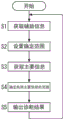
The operation of the diagnosis unit 5 will be described with reference to fig. 6.
First, the diagnosis unit 5 obtains the assistance information (S1). In the present embodiment, the diagnosis unit 5 acquires the sensing results of the output current Io and the input voltage Vi from the current detector and the voltage detector provided in the power conversion circuit 2, respectively, as the auxiliary information.
The diagnosis unit 5 sets a determination range (see fig. 5) based on the assistance information thus obtained (S2). In the present embodiment, the diagnosis unit 5 sets determination ranges (normal range, abnormal range, and attention range) for comparison with the value of the main information, according to the magnitudes of the output current Io and the input voltage Vi as the auxiliary information.
The diagnosis unit 5 obtains the main information (S3). Specifically, the diagnostic unit 5 obtains, as the main information, the sensing result of the internal current I31 flowing through the inductor L31 of the buffer circuit 3 from the current detector provided in the power conversion circuit 2.
Then, the diagnostic unit 5 performs range determination for determining which of the normal range, the abnormal range, and the attention range includes the value of the main information thus acquired, i.e., the value of the internal current I31 (S4). If the value of the main information (the value of the internal current I31) is included in the normal range, the diagnosis unit 5 determines that the power conversion circuit 2 is in the normal state. If the value of the main information (the value of the internal current I31) is included in the abnormal range, the diagnosis unit 5 determines that the power conversion circuit 2 is in the abnormal state. If the value of the main information (the value of the internal current I31) is included in the attention range, the diagnosis unit 5 determines that the power conversion circuit 2 is in the attention state.
The diagnosis unit 5 outputs the diagnosis result to the server 8 through the outputter 51. The server 8 may manage the state of the power conversion circuit 2 in the power conversion system 1 based on the diagnosis result thus received. Thus, for example, when the server 8 receives the diagnosis result that the power conversion circuit 2 is in the attentive state, the administrator of the power conversion system 1 may perform maintenance or the like on the power conversion circuit 2 before the power conversion circuit shifts to the abnormal state. For example, if the power conversion circuit 2 in an abnormal state continues to be used, hard switching or overvoltage application of the switching elements Q11 to Q14, an increase in the electric power extracted by the first clamping circuit 31 of the snubber circuit 3, or the like may damage circuit elements other than the transformer 210. In the power conversion system 1 of the present embodiment, when the power conversion circuit 2 is in the attentive state as the state before shifting to the abnormal state, maintenance can be performed. Therefore, if an abnormality of the power conversion circuit 2 is caused by an abnormality of the transformer 210, the abnormality can be solved only by replacing the transformer 210, thereby suppressing damage to circuit elements other than the transformer 210.
The diagnostic unit 5 repeatedly executes the above-described processes S1 to S4. For example, the diagnostic unit 5 performs the above-described processes S1 to S4 at predetermined cycles (e.g., 10-minute cycles, 1-hour cycles, or 1-day cycles).
Note that, in addition to the diagnosis result, the diagnosis unit 5 may output the value of the main information to the server 8 (S5). Therefore, the transition of the change in the value of the main information can be grasped, and the failure prediction of the power conversion circuit 2 can be performed.
(4) Variants
The above-described embodiments are merely examples of various embodiments of the present invention. Rather, the example embodiments may be readily modified in various ways depending on design choices or any other factors without departing from the scope of the present disclosure.
In the above example, the internal current I31 flowing through the inductor L31 of the buffer circuit 3 is taken as the main information, but the main information is not limited to this example. The primary information includes at least one of a voltage of a terminal of the transformer 210, a voltage generated by the snubber circuit 3, or a current generated by the snubber circuit 3. Thus, the main information may be, for example, the voltage VT2 across the secondary winding wire 212 of the transformer 210 or may be the voltage (bus voltage Vbus) across the winding wires L13, L14. Further, examples of the main information include a voltage across the capacitor C31 (first clamp voltage V31), a voltage across the capacitor C32 (second clamp voltage V32), an input current flowing through the diode D31, and an output current flowing through the diode D32. The diagnosis unit 5 may diagnose the power conversion circuit 2 based on the plurality of pieces of main information.
Further, the above example employs the output current Io and the input voltage Vi of the power conversion circuit 2 as the plurality of auxiliary information, but the auxiliary information is not limited to this example. The auxiliary information may include information of at least any one of input power, output power, or temperature of the power conversion circuit 2. Therefore, the auxiliary information may include, for example, the input current Ii, the output voltage Vo, noise information on the input power and the output power of the power conversion circuit 2, and the like of the power conversion circuit 2. Further, the auxiliary information may include the temperature of the power conversion circuit 2. In this case, for example, the diagnosis unit 5 may modify the determination range (normal range, abnormal range, attention range) according to the temperature of the power conversion circuit 2. Therefore, the diagnostic accuracy of the power conversion circuit 2 can be improved.
Further, the normal range may be changeable. In this case, the power conversion system 1 preferably includes a setting unit 52 (see fig. 1) configured to set the normal range. For example, the setting unit 52 may set (modify) the normal range according to other information than the auxiliary information. The other information is, for example, the accumulated operation time of the power conversion circuit 2. The setting unit 52 further modifies the determination range set according to the auxiliary information according to other information (accumulated operation time). For example, the setting unit 52 modifies the normal range such that the normal range is expanded as the cumulative operation time increases. This enables diagnosis in consideration of the deterioration of the power conversion circuit 2, and the diagnosis accuracy of the power conversion circuit 2 can be improved. Further, the setting unit 52 may be configured to set the determination range (normal range, abnormal range, attention range) in accordance with the setting information from the server 8 as other information. Note that the setting unit 52 is not limited to having a structure provided in the same housing as the diagnostic unit 5, and the setting unit 52 may be provided in another housing. In this case, the setting unit 52 may be configured to communicate with the diagnosing unit 5 through a network (public network 80 or local network), and set the determination range (normal range, abnormal range, attention range) in the diagnosing unit 5 from a remote location.
In addition, in the above-described example, the buffer circuit 3 is constituted by a regenerative buffer circuit that temporarily stores the taken out electric energy when the positive ringing occurs in the bus voltage Vbus of the power conversion circuit 2 and regenerates the electric energy when the negative ringing occurs, but the buffer circuit 3 is not limited to this example. For example, the buffer circuit 3 may be an RDC buffer circuit, which includes: a series circuit of a capacitor and a diode electrically connected between terminals T31 and T32; and a resistor electrically connected in parallel with the diode.
Further, as shown in a of fig. 7, the power conversion system 1 may be electrically connected to the storage battery 6 through a DC/DC converter 60. The DC/DC converter 60 steps up or down the DC voltage output from the battery 6, and outputs the DC voltage to the power conversion system 1. The power conversion system 1 converts a direct-current voltage from the DC/DC converter 60 into a three-phase alternating-current voltage, and outputs the three-phase alternating-current voltage to the power system 7 (see fig. 1). The DC/DC converter 60 is a bidirectional conversion circuit, and boosts or lowers a DC voltage from the power conversion system 1 and outputs the DC voltage to the battery 6.
As shown in B of fig. 7, the photovoltaic cell 6A may also be electrically connected to a direct current bus between the DC/DC converter 60 and the power conversion system 1 through the DC/DC converter 60A. The DC/DC converter 60A steps up or down the direct-current voltage output from the photovoltaic cell 6A, and outputs the direct-current voltage to the power conversion system 1.
Further, the above-described power conversion circuit 2 is configured to output three-phase alternating-current power to the power system 7, but may be configured to output single-phase alternating-current power.
The function similar to the diagnostic unit 5 may be realized by a diagnostic method of the power conversion circuit 2, a computer program, a non-transitory storage medium in which the program is recorded, or the like. A diagnostic method of the power conversion circuit 2 according to an aspect is a diagnostic method of the power conversion circuit 2 including the transformer 210 and the switching element configured to be electrically connected to the transformer 210 and configured to convert power, the diagnostic method including a diagnostic process. The diagnostic process includes diagnosing the power conversion circuit 2 based on at least one of a voltage of a terminal of the transformer 210, a voltage generated by the snubber circuit 3, or a current generated by the snubber circuit 3, the snubber circuit 3 configured to be electrically connected to the transformer 210 and configured to extract electrical energy from the power conversion circuit 2.
The (computer) program according to an aspect is a program configured to cause a computer system to execute a diagnostic method of the power conversion circuit 2.
The power conversion system 1 according to the present disclosure includes a computer system. The computer system includes a processor and memory as the main hardware components. Some functions of the power conversion system 1 according to the present disclosure may be realized by causing a processor to execute a program stored in a memory of a computer system. The program may be stored in advance in a memory of the computer system, may be provided via a telecommunication network, or may be provided as a non-transitory recording medium such as a memory card readable by the computer system, an optical disk, or a hard disk drive storing the program. The processor of the computer system may be constituted by a single or a plurality of electronic circuits including a semiconductor Integrated Circuit (IC) or a large scale integrated circuit (LSI). The integrated circuits such as IC or LSI mentioned herein may be referred to in other ways depending on the degree of integration, and include integrated circuits called system LSI, Very Large Scale Integration (VLSI), or Ultra Large Scale Integration (ULSI). Alternatively, a Field Programmable Gate Array (FPGA) which is programmed after manufacturing an LSI, or a reconfigurable logic device which allows reconfiguration of connections or circuit portions inside the LSI may also be employed as the processor. The plurality of electronic circuits may be concentrated on one chip or may be distributed over a plurality of chips. The plurality of chips may be concentrated in one device or may be distributed among a plurality of devices. As described herein, a computer system includes a microcontroller that includes one or more processors and one or more memories. Thus, a microcontroller is also made up of one or more electronic circuits including a semiconductor integrated circuit or a large scale integrated circuit.
Further, concentrating the various functions of the power conversion system 1 in one case is not an essential structure of the power conversion system 1. The components of the power conversion system 1 may be distributed in a plurality of housings. Further, at least some functions of the power conversion system 1 (e.g., some functions of the diagnosis unit 5 and the like) may be realized by cloud (cloud computing) and the like.
(conclusion)
The power conversion system (1) according to the first aspect includes a power conversion circuit (2), a buffer circuit (3), and a diagnostic unit (5). The power conversion circuit (2) includes a transformer (210) and switching elements (Q11-Q14) configured to be electrically connected to the transformer (210), and the power conversion circuit (2) is configured to convert power. The snubber circuit (3) is electrically connected to the transformer (210) and configured to extract electrical energy from the power conversion circuit (2). The diagnosis unit (5) is configured to diagnose the power conversion circuit (2) based on at least one of a voltage of a terminal of the transformer (210), a voltage generated by the snubber circuit (3), or a current generated by the snubber circuit (3).
According to this aspect, it is determined whether there is an abnormality in the power conversion circuit (2).
In the power conversion system (1) of the second aspect with reference to the first aspect, the diagnosis unit (5) is configured to diagnose the power conversion circuit (2) based on the main information and the auxiliary information. The main information includes at least any one of a voltage of a terminal of the transformer (210), a voltage generated by the snubber circuit (3), or a current generated by the snubber circuit (3). The auxiliary information includes at least any one of input power, output power, and temperature of the power conversion circuit (2).
According to this aspect, the accuracy of diagnosis of the power conversion circuit (2) is improved.
In the power conversion system (1) of the third aspect with reference to the second aspect, the diagnosis unit (5) is configured to determine that the power conversion circuit (2) is in the abnormal state when the value indicated by the primary information is included in an abnormal range that is outside a normal range based on the auxiliary information.
According to this aspect, diagnosis of the power conversion circuit (2) is performed in consideration of the operating condition of the power conversion circuit (2).
In the power conversion system (1) of the fourth aspect with reference to the third aspect, the diagnostic unit (5) is configured to determine that the power conversion circuit (2) is in the attentive state when the value indicated by the primary information is included in an attentive range between the normal range and the abnormal range.
With this aspect, the state before the transition of the power conversion circuit (2) to the abnormality is detected.
In the power conversion system (1) of the fifth aspect with reference to the third or fourth aspect, the normal range is changeable.
With this aspect, erroneous diagnosis of the power conversion circuit (2) is reduced.
In the power conversion system (1) of a sixth aspect with reference to any one of the first to fifth aspects, the snubber circuit (3) is configured to extract electric energy from the power conversion circuit (2) and regenerate the electric energy thus extracted into the power conversion circuit (2). The diagnosis unit (5) is configured to diagnose the power conversion circuit (2) based on at least one of a voltage of a terminal of the transformer (210), a voltage generated by the snubber circuit (3), or a current generated by the snubber circuit (3).
With this configuration, the power loss of the power conversion circuit (2) is reduced. This improves the accuracy of diagnosis of the power conversion circuit (2).
The power conversion system (1) of the seventh aspect with reference to any one of the first to sixth aspects further includes an output device (51) configured to output a diagnosis result of the diagnosis unit (5).
According to this aspect, the state of the power conversion circuit (2) is managed by an external system.
A diagnostic method of a power conversion circuit (2) of an eighth aspect is a diagnostic method of a power conversion circuit (2), the power conversion circuit (2) including a transformer (210) and switching elements (Q11 to Q14) configured to be electrically connected to the transformer (210), the power conversion circuit (2) being configured to convert electric power, the diagnostic method including a diagnostic process. The diagnostic process includes diagnosing the power conversion circuit (2) based on at least one of a voltage of a terminal of the transformer (210), a voltage generated by the snubber circuit (3), or a current generated by the snubber circuit (3), the snubber circuit (3) being configured to be electrically connected to the transformer (210) and to extract electrical energy from the power conversion circuit (2).
According to this aspect, it is determined whether there is an abnormality in the power conversion circuit (2).
The program according to the ninth aspect is configured to cause the computer system to execute the diagnostic method of the power conversion circuit (2) of the eighth aspect.
According to this aspect, it is determined whether there is an abnormality in the power conversion circuit (2).
List of reference numerals
1 power conversion system
2 power conversion circuit
210 transformer
3 buffer circuit
5 diagnostic unit
51 output device
Q11 through Q14 switching elements.
Claims (9)
1. A power conversion system comprising:
a power conversion circuit including a transformer and a switching element configured to be electrically connected to the transformer, the power conversion circuit configured to convert power;
a snubber circuit configured to be electrically connected to the transformer and to extract electrical energy from the power conversion circuit; and
a diagnostic unit configured to diagnose the power conversion circuit according to at least one of a voltage of a terminal of the transformer, a voltage generated by the snubber circuit, or a current generated by the snubber circuit.
2. The power conversion system of claim 1, wherein
The diagnosis unit is configured to diagnose the power conversion circuit according to:
primary information including at least any one of a voltage of a terminal of the transformer, a voltage generated by the snubber circuit, or a current generated by the snubber circuit, and
auxiliary information including at least any one of input power, output power, or temperature of the power conversion circuit.
3. The power conversion system of claim 2, wherein
The diagnostic unit is configured to: determining that the power conversion circuit is in an abnormal state when the value represented by the primary information is included in an abnormal range that is outside a normal range based on the auxiliary information.
4. The power conversion system of claim 3, wherein
The diagnostic unit is configured to: determining that the power conversion circuit is in an attention state when a value represented by the primary information is included in an attention range between the normal range and the abnormal range.
5. The power conversion system of claim 3 or 4, wherein
The normal range can be varied.
6. The power conversion system of any of claims 1-5, wherein
The snubber circuit is configured to extract electrical energy from the power conversion circuit and regenerate the electrical energy thus extracted into the power conversion circuit, and
the diagnosis unit is configured to diagnose the power conversion circuit based on the voltage or current generated by the snubber circuit.
7. The power conversion system of any of claims 1-6, further comprising:
an outputter configured to output a diagnosis result of the diagnosis unit.
8. A diagnostic method of a power conversion circuit, the power conversion circuit including a transformer and a switching element configured to be electrically connected to the transformer, the power conversion circuit configured to convert power, the method comprising:
diagnosing the power conversion circuit based on at least one of a voltage at a terminal of the transformer, a voltage generated by a snubber circuit configured to be electrically connected to the transformer and to extract electrical energy from the power conversion circuit, or a current generated by the snubber circuit.
9. A program configured to cause a computer system to execute the diagnostic method according to claim 8.
Applications Claiming Priority (3)
| Application Number | Priority Date | Filing Date | Title |
|---|---|---|---|
| JP2019053844 | 2019-03-20 | ||
| JP2019-053844 | 2019-03-20 | ||
| PCT/JP2020/009322 WO2020189295A1 (en) | 2019-03-20 | 2020-03-05 | Power conversion system, and diagnosis method and program for power conversion circuit |
Publications (1)
| Publication Number | Publication Date |
|---|---|
| CN113632360A true CN113632360A (en) | 2021-11-09 |
Family
ID=72520837
Family Applications (1)
| Application Number | Title | Priority Date | Filing Date |
|---|---|---|---|
| CN202080022157.8A Withdrawn CN113632360A (en) | 2019-03-20 | 2020-03-05 | Power conversion system, and method and program for diagnosing power conversion circuit |
Country Status (4)
| Country | Link |
|---|---|
| US (1) | US20220181985A1 (en) |
| JP (1) | JPWO2020189295A1 (en) |
| CN (1) | CN113632360A (en) |
| WO (1) | WO2020189295A1 (en) |
Family Cites Families (22)
| Publication number | Priority date | Publication date | Assignee | Title |
|---|---|---|---|---|
| US5959851A (en) * | 1996-09-13 | 1999-09-28 | Thomson Consumer Electronics, Inc. | Switched-mode power supply control circuit |
| JP4585792B2 (en) * | 2004-05-14 | 2010-11-24 | 日本碍子株式会社 | High voltage pulse generator |
| JP4568858B2 (en) * | 2005-03-14 | 2010-10-27 | 富士通テレコムネットワークス株式会社 | Current balance circuit |
| JP4400632B2 (en) * | 2007-02-20 | 2010-01-20 | Tdk株式会社 | Switching power supply |
| US8159160B2 (en) * | 2008-12-30 | 2012-04-17 | International Business Machines Corporation | Apparatus, system, and method for improved fan control in a power supply |
| RU2631664C2 (en) * | 2012-06-19 | 2017-09-26 | Конинклейке Филипс Н.В. | Control modes for resonant dc converter |
| WO2014170976A1 (en) * | 2013-04-17 | 2014-10-23 | 三菱電機株式会社 | Switching power supply circuit and control method therefor |
| JP5938008B2 (en) * | 2013-05-27 | 2016-06-22 | 株式会社デンソー | Power converter |
| JP5987850B2 (en) * | 2014-02-07 | 2016-09-07 | 株式会社デンソー | Power converter |
| JP6575462B2 (en) * | 2016-08-24 | 2019-09-18 | オムロン株式会社 | Voltage converter |
| US10924024B2 (en) * | 2016-09-02 | 2021-02-16 | Panasonic Intellectual Property Management Co, Ltd. | Regenerative power conversion system with inverter and converter |
| JP6675106B2 (en) * | 2016-10-12 | 2020-04-01 | パナソニックIpマネジメント株式会社 | Power conversion system |
| WO2018110440A1 (en) * | 2016-12-12 | 2018-06-21 | パナソニックIpマネジメント株式会社 | Snubber circuit and power conversion system using same |
| CN110546872A (en) * | 2017-04-24 | 2019-12-06 | 松下知识产权经营株式会社 | power conversion system |
| JP7008222B2 (en) * | 2017-04-24 | 2022-01-25 | パナソニックIpマネジメント株式会社 | Power conversion system |
| JP6725758B2 (en) * | 2017-06-06 | 2020-07-22 | 株式会社日立製作所 | Power converter and three-phase power converter |
| US10541621B2 (en) * | 2017-09-12 | 2020-01-21 | Rohm Co., Ltd. | AC/DC converter extracting a forward voltage and a flyback voltage from the secondary winding |
| JP6545310B1 (en) * | 2018-03-22 | 2019-07-17 | 三菱電機株式会社 | Power converter |
| JP6823634B2 (en) * | 2018-11-14 | 2021-02-03 | 矢崎総業株式会社 | Power supply |
| JP6664017B1 (en) * | 2019-02-01 | 2020-03-13 | 株式会社ケーヒン | Temperature detector, abnormality detector, and power converter |
| US11437842B2 (en) * | 2019-03-22 | 2022-09-06 | Seiko Epson Corporation | Power supply control device, switching power supply, and electronic apparatus |
| US11348752B2 (en) * | 2019-05-18 | 2022-05-31 | Amber Solutions, Inc. | Intelligent circuit breakers with air-gap and solid-state switches |
-
2020
- 2020-03-05 WO PCT/JP2020/009322 patent/WO2020189295A1/en active Application Filing
- 2020-03-05 JP JP2021507182A patent/JPWO2020189295A1/ja not_active Withdrawn
- 2020-03-05 CN CN202080022157.8A patent/CN113632360A/en not_active Withdrawn
- 2020-03-05 US US17/440,685 patent/US20220181985A1/en not_active Abandoned
Also Published As
| Publication number | Publication date |
|---|---|
| WO2020189295A1 (en) | 2020-09-24 |
| US20220181985A1 (en) | 2022-06-09 |
| JPWO2020189295A1 (en) | 2020-09-24 |
Similar Documents
| Publication | Publication Date | Title |
|---|---|---|
| EP3267566B1 (en) | Electric power conversion device | |
| EP2352223B1 (en) | System interconnection inverter | |
| US7417842B2 (en) | Apparatus for power conversion in electric rolling stock | |
| US8174849B2 (en) | Electric power converter with soft switching for two way power conversion | |
| WO2009107461A1 (en) | Direct ac power converter | |
| US10778106B2 (en) | Power conversion system | |
| US9692321B2 (en) | Five level inverter | |
| EP2940852A1 (en) | Converter | |
| JP5098522B2 (en) | Inverter device design method | |
| US6940188B2 (en) | Electric power converting device | |
| US11165359B2 (en) | Power conversion system configured to perform power conversion between direct current and three-phase alternating current | |
| US11990830B2 (en) | Power conversion system and virtual DC voltage generator circuit | |
| CN113632360A (en) | Power conversion system, and method and program for diagnosing power conversion circuit | |
| US20220200480A1 (en) | Power conversion system, method for controlling the power conversion system, and program | |
| US20240106322A1 (en) | Power conversion system and control method | |
| JP7122630B2 (en) | Snubber circuit and power conversion system | |
| WO2021186918A1 (en) | Power conversion system, control method for power conversion system, and program | |
| JP6945166B2 (en) | Snubber circuit and power conversion system | |
| JP2022106567A (en) | Charging system | |
| CN117674379A (en) | Power supply with AC/DC random switching function and switching control method | |
| CN114915151A (en) | Power conversion device | |
| JP2019180191A (en) | Snubber circuit and power conversion system | |
| JP2019180192A (en) | Snubber circuit and power conversion system | |
| JP2018196310A (en) | Electric power conversion system |
Legal Events
| Date | Code | Title | Description |
|---|---|---|---|
| PB01 | Publication | ||
| PB01 | Publication | ||
| SE01 | Entry into force of request for substantive examination | ||
| SE01 | Entry into force of request for substantive examination | ||
| WW01 | Invention patent application withdrawn after publication |
Application publication date: 20211109 |
|
| WW01 | Invention patent application withdrawn after publication |