CN1130644C - System and method for maintaining memory coherency in computer system having multiple system buses - Google Patents
System and method for maintaining memory coherency in computer system having multiple system buses Download PDFInfo
- Publication number
- CN1130644C CN1130644C CN97199718A CN97199718A CN1130644C CN 1130644 C CN1130644 C CN 1130644C CN 97199718 A CN97199718 A CN 97199718A CN 97199718 A CN97199718 A CN 97199718A CN 1130644 C CN1130644 C CN 1130644C
- Authority
- CN
- China
- Prior art keywords
- bus
- correlativity
- cache
- memory
- state
- Prior art date
- Legal status (The legal status is an assumption and is not a legal conclusion. Google has not performed a legal analysis and makes no representation as to the accuracy of the status listed.)
- Expired - Fee Related
Links
- 230000015654 memory Effects 0.000 title claims abstract description 454
- 238000000034 method Methods 0.000 title claims abstract description 58
- 238000004891 communication Methods 0.000 claims abstract description 32
- 238000003860 storage Methods 0.000 claims description 108
- 230000008878 coupling Effects 0.000 claims description 21
- 238000010168 coupling process Methods 0.000 claims description 21
- 238000005859 coupling reaction Methods 0.000 claims description 21
- GOLXNESZZPUPJE-UHFFFAOYSA-N spiromesifen Chemical compound CC1=CC(C)=CC(C)=C1C(C(O1)=O)=C(OC(=O)CC(C)(C)C)C11CCCC1 GOLXNESZZPUPJE-UHFFFAOYSA-N 0.000 claims description 19
- 238000012544 monitoring process Methods 0.000 claims description 17
- 238000012986 modification Methods 0.000 claims description 11
- 230000004048 modification Effects 0.000 claims description 11
- 238000012423 maintenance Methods 0.000 claims description 7
- 238000012546 transfer Methods 0.000 claims description 7
- 238000011156 evaluation Methods 0.000 claims description 5
- 238000006073 displacement reaction Methods 0.000 description 16
- 230000015572 biosynthetic process Effects 0.000 description 15
- 238000005755 formation reaction Methods 0.000 description 15
- 230000014509 gene expression Effects 0.000 description 14
- 230000004044 response Effects 0.000 description 13
- 238000010586 diagram Methods 0.000 description 12
- 230000003111 delayed effect Effects 0.000 description 11
- 238000013507 mapping Methods 0.000 description 11
- 238000012545 processing Methods 0.000 description 10
- 238000005516 engineering process Methods 0.000 description 9
- 230000005540 biological transmission Effects 0.000 description 8
- 230000000875 corresponding effect Effects 0.000 description 8
- 230000008569 process Effects 0.000 description 8
- 230000003068 static effect Effects 0.000 description 7
- 230000007246 mechanism Effects 0.000 description 6
- 230000001276 controlling effect Effects 0.000 description 5
- 230000009471 action Effects 0.000 description 4
- 230000008901 benefit Effects 0.000 description 3
- 230000008859 change Effects 0.000 description 3
- 230000005039 memory span Effects 0.000 description 3
- 230000001360 synchronised effect Effects 0.000 description 3
- 235000017060 Arachis glabrata Nutrition 0.000 description 2
- 241001553178 Arachis glabrata Species 0.000 description 2
- 235000010777 Arachis hypogaea Nutrition 0.000 description 2
- 235000018262 Arachis monticola Nutrition 0.000 description 2
- 230000002596 correlated effect Effects 0.000 description 2
- 230000014759 maintenance of location Effects 0.000 description 2
- 230000005055 memory storage Effects 0.000 description 2
- 235000020232 peanut Nutrition 0.000 description 2
- 241001269238 Data Species 0.000 description 1
- 241000254158 Lampyridae Species 0.000 description 1
- 230000003139 buffering effect Effects 0.000 description 1
- 238000013461 design Methods 0.000 description 1
- 230000000694 effects Effects 0.000 description 1
- 239000003550 marker Substances 0.000 description 1
- 230000002093 peripheral effect Effects 0.000 description 1
- 238000002360 preparation method Methods 0.000 description 1
- 238000011084 recovery Methods 0.000 description 1
- 230000009467 reduction Effects 0.000 description 1
- 230000001568 sexual effect Effects 0.000 description 1
Images


Classifications
-
- G—PHYSICS
- G06—COMPUTING; CALCULATING OR COUNTING
- G06F—ELECTRIC DIGITAL DATA PROCESSING
- G06F13/00—Interconnection of, or transfer of information or other signals between, memories, input/output devices or central processing units
- G06F13/14—Handling requests for interconnection or transfer
-
- G—PHYSICS
- G06—COMPUTING; CALCULATING OR COUNTING
- G06F—ELECTRIC DIGITAL DATA PROCESSING
- G06F12/00—Accessing, addressing or allocating within memory systems or architectures
- G06F12/02—Addressing or allocation; Relocation
- G06F12/08—Addressing or allocation; Relocation in hierarchically structured memory systems, e.g. virtual memory systems
- G06F12/0802—Addressing of a memory level in which the access to the desired data or data block requires associative addressing means, e.g. caches
- G06F12/0806—Multiuser, multiprocessor or multiprocessing cache systems
- G06F12/0815—Cache consistency protocols
- G06F12/0831—Cache consistency protocols using a bus scheme, e.g. with bus monitoring or watching means
- G06F12/0833—Cache consistency protocols using a bus scheme, e.g. with bus monitoring or watching means in combination with broadcast means (e.g. for invalidation or updating)
Landscapes
- Engineering & Computer Science (AREA)
- Theoretical Computer Science (AREA)
- Physics & Mathematics (AREA)
- General Engineering & Computer Science (AREA)
- General Physics & Mathematics (AREA)
- Memory System Of A Hierarchy Structure (AREA)
Abstract
A cache-coherent, multiple-bus, multiprocessing system and method interconnects multiple system buses and an I/O bus to a shared main memory and efficiently maintains cache coherency while minimizing the impact to latency and total bandwidth within the system. The system provides coherency filters which coordinate bus-to-bus communications in such a way as to maintain cache memory coherency with a small amount of cross-bus traffic. In addition, the system provides a multiported pool of memory cells which interconnect the multiple buses.
Description
Technical field
The present invention relates to a kind of system and method that in computer system, keeps memory coherency with multisystem bus.
Background technology
In order to improve the performance of the computing machine with single cpu, computer designers has been developed the computing machine with a plurality of cpus.Sometimes, these cpus are connected to each other and are connected with main system memory by single common bus in this multiprocessing computer.Yet recently, the raising of the performance of cpu is faster than the bus performance technology.The central interior processor performance needs more outside bandwidth faster.That is the data total amount of, transmitting on common bus must increase the central handling property that has strengthened to support.As a result, the limited amount that can be connected to the CPU (central processing unit) on the common bus is supported the bandwidth of CPU (central processing unit) and the total bandwidth of common bus in needs.
A kind of method that is reduced in the bus bandwidth of each processor requirement in the multiprocessing system is to place a cache portion between each processor and common bus.The associative cache parts of processor in case data are packed into, this processor does not use common bus with regard to the data in the energy access cache parts.In general, when processor obtained data from its cache portion, less data was by limited common bus bandwidth for transmission.
In many cases, processor will repeatedly be revised specific data value.When each data value is revised, need successively data value to be write back primary memory again.Yet, the data value of revising is write back primary memory again, increased and supported the amount of bus bandwidth that processor needs.Therefore, if the write operation number of times can reduce, need then to support that the bus bandwidth of processor just can reduce.
A kind of cache portion can reduce the write operation number of times, is called " write-back " cache memory.The data value that the interim storage of write-back cache has been revised, thereby reduction writes back the bus transaction number that primary memory needs with data value.For example, processor can repeatedly be revised data value and data need not be write back primary memory in write-back cache.Write-back cache guarantees that the data of having revised are written back to primary memory at last.
When total bus bandwidth that the write-back cache device can reduce very effectively that multiprocessing system needs, unfortunately, write-back cache produces the memory coherency problem.For example, each write-back cache device comprises the copy of its data value.In this case, if a more than processor can be revised a data value independently, the different version of so same data value may be present in the more than write-back cache device.This will produce wrong operation, the result, and some mechanism must guarantee that all processors at any time have the version of a unanimity to all data values.
For example, when processor was revised data value, the data value of having revised before the data value of having revised writes back to primary memory was present in the write-back cache device.In this example, before write-back cache write back to primary memory to the data value of having revised, primary memory and another cache portion comprised the copy of outmoded data value always.Yet, in order to keep data integrity, ask another processor of this data value, must obtain this data value of latest edition, rather than outmoded data value.
Guarantee that all processors have the process of the consistent version of all data value to be called cache coherence.General and the successful raising cache coherence method of one cover depends on alleged " inquiring after operation ".In general, inquire after operation when existing, in cache portion, inquire after bus transaction on this common bus of operation supervise and control when multiple.Content or which affairs of inquiring after which business-impacting cache portion of operation mark relate to the data of having revised that are present in the cache portion.Inquiring after operation generally requires all processors to share a common bus with the cache portion relevant with them.When specific cache portion comprised a data value of having revised, the sharing of common bus allowed cache portion to come the controlling bus affairs and intervene bus transaction effectively.
The cache coherence method is generally also utilized correlativity state information, and whether this information indication specific data value in cache portion is invalid, that revised, that share, occupied specially, or the like.When a lot of cache coherence methods existed, two popular versions comprised MESI cache coherency protocol and MDESI cache coherency protocol.MESI abridges and represents that revised, that monopolize, shared and invalid state, and that MDESI abbreviation expression has been revised, occupied, that monopolize, shared and invalid state.
The implication of state changes to another from a realization.Say that at large the specific cache portion of the state ordinary representation of having revised has been revised specific data value.State of monopolizing and the specific cache portion of occupied state ordinary representation can be revised the copy of data value.The copy of shared state ordinary representation data value may reside in different cache portion, and the data value that disarmed state is illustrated in the cache portion is invalid.
In the operation, cache portion is inquired after bus operation and is used correlativity state information to guarantee cache coherence.For example, suppose first processor, wish to obtain a specific data value with first cache portion.And, suppose second processor with second cache portion, comprise a data value version of having revised (data value of correlativity state information indication in second cache portion is in the state of having revised).
In this example, first processor makes read bus request initialization to obtain this data value, second cache portion is inquired after the read bus request and is determined that it comprises the version of having revised of data value, and second cache portion is inserted and transmitted the data value of having revised then and gives first processor by common bus.According to this system, the data value of having revised can or cannot be write primary memory simultaneously.
In another example, suppose that first processor wishes to occupy specially specific data value.And, suppose that second cache portion comprises a data value copy (correlativity state information representation data value is in shared state in second cache portion) unmodified, that share.In this example, first processor makes the read bus request initialization of request exclusive data.
Second cache portion is inquired after the read bus request and is determined that it comprises the copy of shared data value.Second cache portion becomes disarmed state by the correlativity state information with data value then makes its shared data value invalid.The correlativity state of data value is become disarmed state makes the data value in second cache portion invalid.The copy that first processor is finished the read bus request then and obtain this data value from primary memory is with special use.
In having the multiprocessing system of single common bus, when inquiring after operation when keeping cache coherence, have that more powerful computing machine comprises a more than bus so as each bus with have polyprocessor primary memory interconnection; Yet because common bus has the limits to growth of the processor number that it can support, multiple bus system has the performance standard of necessary realization requirement.Problem relevant with multibus is that the processor on a bus can not be monitored by the initialized affairs of the processor on other buses.As a result, inquire after operation and can not in the multibus computing machine, keep memory coherency.
Keeping a kind of method of cache coherence in multiple bus system is that the bus transaction in each bus initialization is expanded to other all buses.Unfortunately, this method causes the combination bus bandwidth load of all buses to be transferred to each bus.Positive according to expectation, this has significantly reduced system performance side by side except the benefit of multibus.
Second method is based on the cache coherence method that is known as root directory.IEEEScaleableCoherentInterconnect is the example of a multibus root directory cache coherence system, and under directory pattern, this processor is not inquired after bus transaction.On the contrary, main memory subsystem keeps memory coherency by storing the extra information that has real data.
Extraneous information in main memory subsystem generally is expressed as 1) which processor or which processor obtained the copy of a data value, 2) the correlativity state of this data value.For example, extra information can indicate a more than processor to share same data value.In another example, extra information can be indicated has only single processor to have the right of revising an accurate data value.
When processor request msg value, main memory subsystem determines whether it has the latest edition of this data value.If no, main memory subsystem transmits up-to-date data value and gives request handler from the processor that has up-to-date data value.Perhaps, primary memory energy indication request processor, other which processors have up-to-date data value.
Because the information about the position of the up-to-date version of each data value is preserved by main memory subsystem, so this processor does not need " inquiring after " bus transaction.Yet, keep this catalogue, can increase expense to system, this is owing to be necessary for the cause of the additional information of each data value maintenance in primary memory.In addition, for each data value maintenance catalogue in the primary memory also can make system performance reduce, this is because the cause that the data that need location and transmission to need are given the time of request handler.
The system of another kind of root directory should be a bus interconnection, the relevant correlativity state information of data value that its storage is interior with in fact being stored in cache portion.Like this, be not to increase and the storer (as pattern) of proportional increase, but memory space only relate to the smaller szie of the cache portion of combination based on catalogue with primary memory.Yet this method needs multiple bus system to come the double copy of the correlativity state information that storage is relevant with all data values in each cache portion.
For example, SunMicrosystem ' sUltraSparc system uses the bus switch multibus that interconnects, wherein each bus is communicated by letter with the processor with internally cached parts, and bus switch keeps the double of the correlativity state information relevant with all data value in the cache portion to copy.In the UltraSparc system, bus switch can keep correlativity state information double copy, because in the UltraSparc system, processor is configured to provide information accurately, and promptly that data value just is replaced and allows the External Cache mark to be held.
Yet this bus switch is not suitable for many existing processors, because they do not export cached data replacement information accurately.For example, many conventional processing machines only keep correlativity state information accurately in their internally cached parts.Like this, other equipment can not determine when internally a data value shifts out in the cache portion, and about the accurate information of the correlativity state information in the internally cached parts, bus switch can not keep the double copy of correlativity state information.
Summary of the invention
The invention provides a kind of high-speed cache is correlated with, multiple bus system, this system increases total processor performance limit of unified bus system effectively.The present invention knows that multibus, multiprocessing system need a kind of low latency, high bandwidth system communication, this system 1) with the multisystem bus and many I/O equipment interconnects with shared main storage and 2) keep cache coherence effectively and reduce influence stand-by period in the system and total bandwidth.Attached invention illustrates these problems with " correlativity wave filter ", " correlativity wave filter " allow bus-to-bus communication is arranged side by side, keep the cache memory correlativity by this way and reduce the excessive of the crossover bus traffic.
According to an invention of the present invention, a kind of multibus, multiprocessing system comprise:
A kind of system storage;
First bus that a kind of and described system storage is communicated by letter, described first bus has at least one cache memory and its coupling, described cache memory is configured to store a plurality of data values that obtain from described system storage, described cache memory also is configured to keep the cache coherence information that has the data value of first group of correlativity state about described;
The correlativity storer of a kind of and described first bus communication, described correlativity storer are configured to the correlativity state record that keeps relevant with described data value;
Second bus that a kind of and described system storage is communicated by letter, described second bus energy transfer bus affairs; And
The correlativity wave filter that a kind of and described second bus is not connected with described first bus with the record communication of described correlativity state, described correlativity wave filter be configured to monitor described on described second bus bus transaction and according to the crossover bus affairs of described correlativity state recording prohibition from described second bus to described first bus.
According to another aspect of the present invention, a kind of cache coherence method that keeps in multiple bus system comprises:
Keep be present in cache portion in more than first cache state information that data value is relevant, this cache portion is coupled to first bus;
Keep the first bus correlativity state record relevant with described more than first data value;
Monitor bus transaction on described first bus with the first correlativity wave filter;
Monitor bus transaction on second bus with the second correlativity wave filter;
Be transmitted in the bus transaction on described second bus; And
Forbid crossover bus affairs from described second bus to described first bus with the second correlativity wave filter, the at this moment described first bus correlativity state record sheet shows that memory coherency is not to forbid due to the described crossover bus affairs.
Another invention according to the present invention, a kind of multibus, multiprocessing system comprise:
A kind of system storage;
The system bus that a kind of and described system storage is communicated by letter, described system bus has at least one cache memory and its coupling, described cache memory is configured to store a plurality of data values that obtain from described system storage, described first system bus can transmit the multibus affairs;
The correlativity storer that a kind of and described system bus is communicated by letter, described correlativity storer are configured to the system bus correlativity state record that keeps relevant with described data value;
The input/output bus that a kind of and described system storage is communicated by letter, described input/output bus can transmit the multibus affairs; And
The I/O correlativity wave filter of a kind of and described input/output bus and described correlativity memory communication, described I/O correlativity wave filter is configured to monitor the described bus transaction on described input/output bus, and do not monitor bus transaction on described system bus, described I/O correlativity wave filter also is configured to according to the crossover bus affairs of described system bus correlativity state recording prohibition from described input/output bus to described system bus.
Another aspect according to the present invention, a kind of method that keeps cache coherence in multiple bus system comprises:
Keep be present in the cache portion that is coupled to system bus in more than first cache state information that data value is relevant, described cache state information is based on first group of correlativity state;
Keep the correlativity state record relevant with described more than first data value;
Monitor bus transaction on the described system bus with the first correlativity wave filter;
With the bus transaction on the second correlativity wave filter monitoring input/output bus;
Be transmitted in the bus transaction on the described input/output bus; And
Forbid crossover bus affairs from described input/output bus to described system bus with the described second correlativity wave filter, at this moment described correlativity state record instruction memory correlativity will can't help to forbid that described crossover bus office causes.
According to other aspect of the present invention, a kind of multibus, multiprocessing system comprise:
A kind of system storage;
First system bus of communicating by letter and second system bus with described system storage, described first system bus has at least one cache memory and its coupling, and described second bus has at least one cache memory and its coupling, and described cache memory is configured to store a plurality of data values that obtain from described system storage;
The first correlativity storer that a kind of and described first system bus is communicated by letter, the described first correlativity storer is configured to keep and the first relevant correlativity state record of described data value in the described cache portion, and described cache portion is connected with described first system bus;
The second correlativity storer that a kind of and described second system bus is communicated by letter, the described second correlativity storer is configured to keep and the second relevant correlativity state record of described data value in described cache memory, and described cache memory is connected with described second system bus;
The first correlativity wave filter of a kind of and described first system bus and the described second correlativity memory communication.The described first correlativity wave filter is configured to monitor the bus transaction on described first system bus, and forbids the crossover bus affairs based on described second correlativity state record from described first system bus to described second system bus; And
The second correlativity wave filter of a kind of and described second bus and the described first correlativity memory communication, the described second correlativity wave filter is configured to monitor the bus transaction on described second system bus, and forbids the crossover bus affairs based on described first correlativity state record from described second system bus to described first system bus.
According to aspect in addition of the present invention, a kind of multibus, multiprocessing system comprise:
A kind of system storage;
First bus that a kind of and described system storage is communicated by letter and second bus, described first bus has the cache memory of at least one and its coupling, and described second bus has the cache memory of at least one and its coupling, described cache memory, the a plurality of data values that obtain are stored in configuration from described system storage, described cache memory also disposes the cache coherence information that keeps about described data value;
A kind of first correlativity memory devices is used for keeping the first correlativity state record of the described data value relevant with described first bus;
A kind of second correlativity memory devices is used for keeping the second correlativity state record of the described data value relevant with described second bus;
A kind of first correlativity filter apparatus is used for monitoring the bus transaction on described first bus, and forbids from described first bus to described second bus based on the crossover bus affairs of described second correlativity state record; And
A kind of second correlativity filter apparatus is used for monitoring the bus transaction on described second bus, and forbids from described first bus to described second bus based on the crossover bus affairs of described first correlativity state record
According to aspect in addition of the present invention, a kind of multibus, multiprocessing system comprise:
A kind of system storage;
First bus that a kind of and described system storage is communicated by letter, described first bus has the cache memory of at least one and its coupling, described cache configuration is stored a plurality of data values that obtain from described system storage, described cache memory also disposes the correlativity state information that keeps about described data value;
The correlativity storer of a kind of and described first bus communication, described correlativity memory configurations keeps the correlativity state record relevant with the described data value that has second group of correlativity state, and wherein said second group of correlativity state is different from described first group of correlativity state;
Second bus that a kind of and described system storage is communicated by letter.Described second bus energy transfer bus affairs;
The correlativity wave filter of a kind of and described second bus and described correlativity memory communication, described correlativity filter configuration is monitored the bus transaction on described second bus, and do not monitor bus transaction on described first bus, described correlativity filter configuration is forbidden from described second bus to described first bus based on the crossover bus affairs of described correlativity state record.
According to aspect in addition of the present invention, a kind of cache coherence method that keeps in multiple bus system comprises:
Keep be present in cache portion in more than first cache state information that data value is relevant, described cache portion is coupled to first bus, described cache state information is based on first group of correlativity state;
Keep the correlativity state record relevant with described data value, described correlativity state record is based on second group of correlativity state, and wherein said second group of correlativity state is different from described first group of correlativity state;
Monitor bus transaction on described first bus with the first correlativity wave filter;
Monitor bus transaction on described second bus with the second correlativity wave filter;
Be transmitted in the bus transaction on described second bus; And
Forbid crossover bus affairs from described second bus to described first bus with the described second correlativity wave filter, at this moment described correlativity state record instruction memory correlativity is not by forbidding that described crossover bus office causes.
According to a further aspect of the invention, a kind of multibus, multiprocessing system comprise:
A kind of system storage;
First bus that a kind of and described system storage is communicated by letter and second bus, described first bus has a plurality of cache memories with its coupling, and described second bus has a plurality of cache memories with its coupling, described cache memory is configured to carry out inquires after operation and a plurality of data values maintenance cache state informations for obtaining from described system storage, described cache memory also is configured to the internal modification described cache state information relevant with some described data value and does not export described internal modification;
The correlativity storer of a kind of and described first bus communication, described correlativity storer are configured to the correlativity state record that keeps relevant with the described described data value that is obtained by the cache memory on described first bus; And
The correlativity wave filter of a kind of and described second bus and described correlativity memory communication, described correlativity wave filter is configured to monitor the bus transaction on described second bus, and do not monitor bus transaction on described first bus, described correlativity wave filter also is configured to forbid from described second bus to described first bus based on the crossover bus affairs of described correlativity state record.
According to aspect in addition of the present invention, a kind of cache coherence method that keeps in multiple bus system comprises:
Keep be present in cache portion in more than first cache state information that data value is relevant, this cache portion is coupled to first system bus;
Internal modification in described cache portion described cache state information and do not export described internal modification;
Keep the correlativity state record relevant with described data value;
With the correlativity wave filter monitoring bus transaction on second bus, and do not monitor bus transaction on described first bus,
Transmit the bus transaction on described second bus; And
Forbid the crossover bus affairs from described second system bus to described system bus, at this moment described correlativity state record instruction memory correlativity can't help to forbid that described crossover bus office causes.
In the preferred embodiment of the invention, system bus, I/O bus and memory member are by the coupling of multiport bus switch.This bus switch not only connects any system bus or the I/O bus arrives any memory member, and handles the crossover bus traffic.In addition, preferred bus switch comprises bus interface logic, and this logic need to determine the operation of answer bus affairs.Yet, the invention is not restricted to this multiport bus switch and can be used in multiple other bus interconnections, for example, when independently bus bridge is used for data routing.
In multibus, multiprocessing system, in order to guarantee cache coherence, each supports the bus of Cache to have the correlativity wave filter of a distribution.Each correlativity wave filter comprises the marking of control device, rotary encoder and rule list.In addition, each correlativity is filter coupled to mark memory.In general, each marking of control device and all mark memory interfaces.Each rotary encoder determines which kind of bus transaction is just occurring on the distribution bus of rotary encoder, and each rule list determines that what bus transaction or affairs group must keep cache coherence.
Now, mark memory, each mark memory keeps following record: the 1) address of the data value in the cache portion that is positioned to be connected with the distribution bus of mark memory, and 2) the cache coherence state relevant with data value.As everyone knows, each data value in primary memory identifies with the respective memory address.In a preferred embodiment, mark memory storaging mark data value, rather than the data value address of actual data value.Except that storage data value address, preferred mark memory is also stored the correlativity state information relevant with the data value address.
For example, suppose that the first correlativity wave filter and first mark memory distribute to first bus.Also suppose first processor request msg value from primary memory on first bus.The first correlativity wave filter remains on the record of the storage address in first mark memory.In addition, the first correlativity wave filter is also stored and the relevant correlativity state information of storage address in first mark memory.
Data total amount accessed in memory transaction is from the system to the system change.In the most conventional system, when the processor execute store was read affairs, the enough storer of this processor visit was with the part of the internal cache of filling this processor.In general, internal cache is stored the multidata value in the cache line that is called.
As everyone knows, the storer in conventional computer processing system is divided into 8 bit quantity (byte), 16 bit quantity (word) and 32 bit quantity (double word).In many 32 current bit processing machines, primary memory is designed to double word (32) border.In most of 32 bit processing machines, each cache line can keep how double word.
Generally speaking, when processor request msg value, this processor obtains enough data to fill whole cache line.For example, in the PentiumPro processor, each internal data value changes on length, but is no more than 64 positions.Yet the cache line of PentiumPro keeps 32 bit byte data (256).When the PentiumPro processor wished to obtain data value from primary memory, it generally obtained 8 data values (256) that need to fill a cache line.
In conventional system, each cache line is identified by cache line address.For example, in the PentiumPro system, cache line have with cache line in the identical cache line address of storage address of minimum data value.Yet, because each cache line comprises 32 bit byte data, so the cache line address of each cache line is short and do not comprise 5 lowest address positions.In a preferred embodiment, each distributes to the mark memory storage cache line address of specific bus.
Except that storage cache line address, each mark memory is also stored the correlativity state relevant with cache line address.The correlativity state relates to the cache line state in the cache portion.In a preferred embodiment, the correlativity state comprises three different correlativity states: disarmed state, shared state or occupied state.
Disarmed state represents that cache line high-speed cache inlet invalid and the storage cache line is empty and can stores new cache line.Shared state represents that processor has the copy of cache line, but does not have the power of amendment.The shared cache line for example, is programmed instruction or the main read data project that is not modified often.Occupied state representation cache line can be obtained the processor of cache line and be revised.
Yet it is invalid that those of ordinary skill in the art is appreciated that the correlativity state of cache line not only is limited to, and shares and occupied agreement.In fact, skilled in the art will recognize that, the correlativity state may be realized with large-scale coherency protocol, as that revised, that monopolize, shared and invalid (MESI) agreement, that revised, that monopolize, special-purpose, shared and invalid (MDESI) agreement, that revised, that share, invalid (MSI) agreement, invalid and the occupied agreement of two condition, the Berkeley agreement, the UniversityofIllinois coherency protocol, the Firefly agreement of digital device, the XeroxDragon agreement, or the like.Invalid, shared and occupied agreement that preferred embodiment has been utilized, this is because it can be connected with the PentiumPro processor that utilizes the MESI agreement effectively.
In many conventional processing machines, these processors have internally cached parts, and internally cached parts are not exported about being stored in the state of the correlativity accurately information of the cache line in the internally cached parts.For example, internally cached parts can be discarded unmodified cache line and not send the signal that cache line has gone out of use.In another example, internally cached parts can obtain and have the cache line that cache portion does not have the modification right of priority of modification.In this example, cache portion can be discarded cache line and do not sent the signal that cache line has gone out of use.As a result, the equipment of monitoring cache portion can think that cache portion has a copy of having revised of cache line, and at this moment cache line has in fact been discarded cache line.Yet in preferred embodiments of the invention, each mark memory is adapted to guarantee cache coherence for the internally cached parts of not exporting current correlativity state information especially.
An importance of the present invention is each mark memory by keep may the current superset that remains on the cache line address in the internally cached parts, guarantees cache coherence.Like this, the superset of the cache line address in mark memory can indicate the specific cache line in cache portion to be in shared state, and at this moment cache portion has in fact been discarded cache line.In other cases, the superset of mark memory high speed cache line address can indicate cache line specific in the cache portion to be in the state of having revised, and at this moment, device when cache portion has in fact write back to primary storage with cache line.
In order to keep the superset of cache line address, preferred correlativity wave filter uses the rule that contains that is called.Contain the regular cache line address that guarantees to be stored in the cache portion that is connected with specific bus and always distribute to the subclass of the cache line address in the mark memory of bus.Because each correlativity wave filter is monitored the cache line of all relevant bus access by it, so the address relevant with each accessed cache line is held in the mark memory of distributing to bus.When cache line address is must be from a mark memory deleted, contain the relevant cache portion of rule indication from their cache memory, to delete cache line.
For example, when mark memory does not have memory span when keeping new cache line address, must come in mark memory, to prepare the space by from mark memory, getting rid of an existing cache line address (old cache line address) for new cache line address.If old cache line address is in disarmed state (cache portion that connects with bus does not re-use the cache line relevant with old high-speed cache address), distributes to the correlativity wave filter of mark memory and replace old cache line address with new cache line address simply.
Yet when old cache line address was in shared or occupied state, the correlativity wave filter can not be got rid of old cache line address from mark memory, make old cache line address invalid up to cache portion.As mentioned above, preferred mark memory keeps the cache line address superset, and old like this cache line address must at first be disabled in cache portion before old cache line address can replace it with new cache line address.
The correlativity wave filter makes the old cache line address in the cache portion invalid by carrying out the invalidation bus affairs.The invalidation bus affairs indicate the cache portion that connects with bus to make the old cache line address cache line relevant with it invalid in inside.
For example, suppose that first processor with first cache portion and second processor with second cache portion are connected to first bus, first bus has a correlativity wave filter that is assigned with and a mark memory.And, suppose that first cache portion comprises first cache line that is in shared state.In this example, mark memory comprises first cache line address and shared state information.In addition, suppose the read bus affairs of the second processor initialization requests, the second speed buffering row.At last, suppose that mark memory does not have memory span to give second cache line address.
In this example, need to get rid of first cache line address be that second cache line address is prepared the space to the correlativity wave filter.Yet before the correlativity wave filter can be got rid of first cache line address, the correlativity wave filter must be carried out the invalid bus transaction of first cache line address that makes in first cache portion.In order to make the first high-speed cache address line invalid, the correlativity wave filter is carried out invalidation bus affairs, and these invalidation bus affairs indicate first cache portion so that the cache line relevant with first cache line address is invalid.
When carrying out the invalidation bus affairs, the correlativity wave filter suspends the read bus affairs that are used for second cache line address, because first cache line address is in shared state (first cache line is not modified), the first cache portion invalid response bus transaction also makes first cache line invalid.Finish after the invalidation bus affairs, the correlativity wave filter is replaced first cache line address in the mark memory with second cache line address.
Yet under certain conditions, first cache portion may be revised first cache line (for example, first cache line is in occupied state).If first cache line is in occupied state, the first correlativity wave filter is carried out the invalidation bus affairs that make first cache line invalid again.Yet if first cache portion has been revised first cache line, first cache portion is come the invalid response bus transaction by carrying out the write bus affairs, and first cache line that these write bus affairs will have been revised writes back to primary memory.
After first cache line that will revise write back to primary memory, first cache portion made first cache line invalid.The correlativity wave filter is then with first cache line address in second cache line address replacement mark memory.Like this, under certain conditions, remain on the data that to have revised before the cache line of a superset requirement cache portion in the invalid flag storer of the cache line address in the mark memory and write back to primary memory.
In a preferred embodiment, each correlativity wave filter uses the cache line address in the direct mapping technique storage mark storer.Directly mapping technique specifies each cache line address by map specific markers inlet in the mark memory.When although preferred embodiment is used direct mapping technique, those of ordinary skill in the art knows that many different technology can be used to set the cache line address in the mark memory.For example, substitute direct mapping technique, mark memory can use relevant mapping technique fully.In a complete related system, any cache line address can be present in any mark inlet.In other embodiments, each cache line address can only be stored in one of two different mark inlets (two-way group of association), and perhaps four different marks enter the mouth one of (association of four-way group), or the like.
Now, the direct mapping technique in the preferred embodiment.Each cache line address identifies the specific markers inlet as index.In a preferred embodiment, the definition of the inlet number in the mark memory is called the length of flag page.Preferably, the mark memory that is coupled on each system bus has same flag page length.Flag page length is relevant with total cache memory amount of the high-speed cache of this processor.And the mark memory that is coupled to the I/O bus is less on length, and this is because generally be coupled to the little cache portion of I/O bridge.
Flag page should not obscured with the primary memory page or leaf.As everyone knows, in the art, the physical memory address space of computing machine generally can be set as the many sectors that are called storage page, and wherein each storage page comprises the multi-cache line.Storage page is by disposal system definition and be flag page independently.
In a preferred embodiment, cache line address sign 1) flag page, it comprises cache line address, 2) the cache line address position in flag page.Especially, the high-order identity marking page or leaf in the cache line address and low level are identified at the cache line address position in the flag page.
In general, low level is called as index, because the internally cached line of low level identity marking address location.For example, for first cache line address in first flag page, upper address bits identifies first flag page, the first cache line address position in the low address bit-identify first note page or leaf.
In a preferred embodiment, the marking of control device in the correlativity wave filter directly arrives mark memory with the cache line address map.For example, when the bus transaction of the specific cache line address of the processor initialization requests that is connected with first bus, the first marking of control device is estimated cache line address.The first marking of control device uses than the low address position and enters the mouth with the specific markers that identifies in first mark memory as index.The first marking of control device is storage high-order (flag page) in the mark inlet that has identified then.
In a preferred embodiment, mark memory is realized with static memory.Static memory realizes allowing each marking of control device each mark memory of fast access during bus transaction.And the present invention is applied to static memory, and those of ordinary skill in the art knows that also dissimilar storing mechanisms can be used to realize mark memory.Preferably, dissimilar storing mechanism can provide access speed that storer equates with Bus Clock Rate to reach optimum performance.
When two cache line address maps entered the mouth to same mark, the cache line address that the marking of control device is got rid of formerly was that new cache line address is prepared the space.As mentioned above, this process can postpone the bus transaction relevant with new cache line address, is disabled up to old cache line address.And invalid old cache line address can require the additional busses affairs to guarantee that mark memory keeps a cache line address superset that is present in the cache portion.
In one embodiment of the invention, each correlativity wave filter also comprises dead queue, and this formation keeps old cache line address not suspend the bus transaction relevant with new cache line address with new cache line address.This can improve system performance, and invalid invalidation bus affairs can occur in later because make old cache line.
Now, keep cache coherence in multibus, when preferred correlativity wave filter needs the crossover bus affairs when determining bus transaction on their distribution bus of monitoring.Especially, the rotary encoder in each correlativity wave filter is monitored the bus transaction on each bus that is assigned with that occurs in the correlativity wave filter.In a preferred embodiment, rotary encoder uses the bus monitor logic of known controlling bus control row.Rotary encoder transmits 1 then) type and 2 of bus transaction) cache state information in the mark memory relevant with bus transaction is to the association rules table.
Now, rule list, rule list determine when and carry out the crossover bus affairs to guarantee cache coherence.In a preferred embodiment, rule list determines whether the crossover bus affairs of operating part according to the correlativity state information in the mark memory.For example, if the bus on first bus is read the specific cache line address of Transaction Identifier, then distribute to the correlativity state of the rule list evaluation of first bus in (global flag storer) cache line address of the mark memory of distributing to another bus.
Be used to the correlativity state information in the global flag storer, rule list determines whether the remote bus affairs must guarantee cache coherence.As described in more detail below, in specific correlativity wave filter, marking of control device visit global flag storer and input cached state are in rule list.In addition, rotary encoder determines that bus transaction type and input bus transaction information are to rule list.
In a preferred embodiment, rule list works as big truth table.Use bus transaction information and global flag memorizer information, rule list determines which crossover bus affairs or bus transaction group must keep cache coherence.
For example, suppose read bus affairs on processor initialization first bus.In this example, first bus of initialization bus affairs refers to local bus, and another bus in the multiple bus system is called as remote bus.The cache line address of read bus affairs transmission requirement is given the correlativity wave filter (local correlations wave filter) of distributing to local bus.Whether the local correlations wave filter is estimated cache line address then and is present in the mark memory (global flag storer) of distributing to remote bus.
The correlativity state of the cache line address that the global flag storer indication in this example requires is a disarmed state.In this case, there is no need to carry out the crossover bus affairs and keep cache coherence, because the cache line address in the remote bus is invalid.Therefore, the local correlations rule list limits bus transaction to local bus and primary memory, does not produce bus transaction on remote bus.Bus transaction is limited to local bus, reduce the crossover bus traffic.
Yet, if the indication of global flag storer needs crossover bus affairs, rule list to determine suitable crossover bus affairs or the transaction set in order to guarantee that cache coherence needs.For example, it is occupied state that a global flag storer can be indicated cache line address, and like this, the cache portion that is connected with remote bus may have a cache line version of having revised.If global flag storer indication cache line address is in occupied state, the bus read command that bus master controller (busmaster) logic that the indication of local rule table is connected with remote bus need be carried out on remote bus guarantees cache coherence.
When the bus read command carried out on remote bus, the remote cache parts are inquired after the bus read command and are determined whether they have the cache line version of a requirement of having revised.If remote cache parts on the remote bus return a cache line version of having revised, then the rule list forward transmits cache line to the request handler on the local bus.
Yet, if the neither one cache portion has been revised cache line on the remote bus, not response bus read command of cache portion.Rule list determines that then up-to-date cache line is present in the primary memory.Therefore, the present invention is transmitted cache line up-to-date in the primary memory to the request handler on the local bus.Like this, the cache line address superset in the preferred embodiment of the invention usage flag storer determines when needs the crossover bus affairs to keep cache coherence.
Another aspect of the present invention comprises the 3rd bus, is used to connect input-output apparatus.In a preferred embodiment, this 3rd bus is called I/O (I/O) bus.Preferred I/O bus and another processor bus are same type bus; Yet those of ordinary skill in the art knows that each processor bus of I/O bus and other can use different bus protocols.
Preferred I/O bus is to operate with the similar mode of other processor bus.Most of I/O transmission send with direct memory visit (DMA) and finish in high-performance computer.DMA transmits usually by the I/O device initialize, directly mobile data and the directly CPU (central processing unit) intervention between primary memory and I/O equipment of I/O equipment.Occur on the I/O affairs of I/O bus keep memory coherency avoid before each DMA transmits and afterwards the cache line in the cache portion overflow
The I/O of another type transmits and comprises the data by the direct programmatic access I/O of processor.In preferred the realization, the bus switch forward transmits that direct I/O sends the I/O bus to and forward transmits all memory accesses, rather than transmits for the I/O bus as the I/O of memory map to the visit in main memory address space.This I/O transmits and do not comprise cache coherence, and is still as described in more detail below, transmitted in a particular manner to another bus from a bus.
Preferred I/O bus comprises I/O correlativity wave filter and I/O bus interface, and the I/O bus interface improves the I/O map and passes through multisystem bus and raising I/O data processing and reduce the system bus complicacy.The I/O data transactions that occurs on the bus is automatically sent to the I/O bus.In addition, the affairs that on the I/O bus, produce be sent to the purpose bus and not the expansion bus affairs give another bus.
Another aspect of the present invention is optimized the communication between multibus.For example, conventional bus switch is with different buses and the interconnection of separate connection path.Like this, in conventional multiple bus system, the common and separate connection path interconnection of first bus and second bus, first bus and the 3rd bus and the interconnection of another separate connection path, and second bus and the 3rd bus also interconnect with another separate connection path.As expected, this independently access path increases the complicacy that bus switch realizes.
For example, when first bus wished to transmit first bus transaction to second bus, first bus was positioned over first formation with first bus transaction, and this first formation is connected first bus with second bus.Second bus is obtained first bus transaction then from the output of first formation.When second bus wished to transmit second bus transaction to first bus, second bus was positioned over second formation with second bus transaction equally, and second formation is connected second bus with first bus.First bus is obtained second bus transaction then from the output of second formation.
Therefore, two formations of two bus requests.When interconnecting, additional busses needs more formation.For example, in a three-bus system, each bus-to-bus connects needs two formations.As a result, three-bus system needs six formations.
Yet, in a preferred embodiment, use the specific method of bus switch, with reducing this system complexity by the memory cell multiport pond of all bus access, utilize the bus switch of this uniqueness, data can flow to any other bus and not interfere other simultaneous data to transmit from any bus.As described in more detail below, the bus transmission that comes from each bus enters the common memory unit cells.Bus transaction in the common memory pond is transmitted to their purpose bus then.Advantageously, any bus can be read or writes to any other bus from any other bus, and does not use the separate connection path.
In a preferred embodiment, relevant with each bus transaction information is stored in three different memory cells that are known as data cell, request unit and address location.The data that the data cell storage is relevant with bus transaction.Request unit comprises bus transaction information, and the bus transaction information definition sends the type of the bus transaction of purpose bus to.At last, address location comprises the address information and the correlativity state information of relevant bus transaction.
In a preferred embodiment, one-to-one relationship is present in each data cell, between each request unit and each address location.Each data cell, request unit or address location like this, perhaps any combination in these unit can be included as the information of specific bus transaction.And preferred embodiment uses three memory cells to keep bus transaction information.Bus transaction information may be present in and be less than or surpass three memory cell.
Generally, data cell, request unit and address location can be regarded as being present in the single pond of multiport memory.Although in a preferred embodiment, data cell, request unit and address location are positioned at different unit, they continue to keep their one-to-one relationship.In a preferred embodiment, the data-interface impact damper comprises data cell and system's access controller comprises address location and request unit.
Now, preferred data-interface impact damper, each data cell in the data-interface impact damper is that multiport also can be by all bus access.Each data cell comprises the data relevant with specific bus transaction.Advantageously, data cell pond in the data-interface impact damper and bus data path interconnection.
Now, preferred systems access controller, system controller comprise central required list, buffer-manager, a plurality of bus master controller and a plurality of bus slave.As everyone knows in this field, the bus transaction initialization that each bus master controller will be on one of bus and each bus slave receives the bus transaction by another device initialize that is connected to one of bus.Central authorities' required list keeps the request unit pond, and buffer-manager keeps the address location pond.
Each request unit in central required list is a multiport and by all bus access.Each request unit comprises the target bus identifier, also is known as action code and occupant's bus identifier of bus transaction code.The purpose bus that target bus identifier sign is specific, the bus transaction that the bus transaction marking code is specific and occupant's bus identifier identify the bus of making a start.
Now, the pond of the address location in the buffer-manager.Each address location be multiport and comprise "-use " information, storage address and data cell status information.Indicate whether that in-use information address location can use in the address location.In a preferred embodiment, be included in-use the position in-use information ,-position used to be set to indicate whether that address location is in uses or idle condition.Under certain conditions, when-when using the position to be set to the free time, valid data may reside in data cell.This allows to optimize, and it re-uses the active data in the idle data unit.
On the other hand, storage address comprises the storage address relevant with bus transaction and data mode in the data cell state designation data unit.Except that the address location pond, buffer-manager also comprises the address location priority encoder, many first in first out (FIFO) storer and multiaddress comparer.The address location priority encoder determines which address location is using and which address location is idle to receive new bus transaction information.In a preferred embodiment, the address location priority encoder determines that in-use information which address location is idle by estimating in each address location.
The address location priority encoder determines that not only which address location is idle.And distribute idle address location to give different buses, more preferably, the address location priority encoder distributes idle address location to give different buses.Distributing idle address location to after the bus, it is not idle with the indication address location that the address priority scrambler is set in-uses the position.For example, suppose in three bus systems that priority encoder determines that three address locations are idle.Preferred priority encoder distributes the first idle address location to give first bus, and the second idle address location gives the 3rd bus for second bus and the 3rd idle address location.
When four-address unit became the free time, the address location priority encoder was circulated back to first bus and distributes four-address unit to give first bus.When preferred address location priority encoder used this technology to distribute idle address location to give different buses, those skilled in the art were appreciated that the address location priority encoder can utilize large-scale allocation model to distribute idle address location to give different buses.
Now, the FIFO storer in the buffer-manager, the address location that the interim storage of FIFO storer is assigned with up to them by bus requirements.In a preferred embodiment, FIFO memory storage address element identifier (element ID), the address location that this identifier sign is assigned with.The address location identifier is a kind of data variable, and it comprises the memory location of the address location that is assigned with.Bus uses the address location identifier with the address location memory location of visit by address location identifier sign.
In a preferred embodiment, each FIFO memory allocation is given specific bus.And each FIFO storer is coupled to one of bus slave and distributes to same bus as one of correlativity wave filter of each FIFO storer.When one of one of bus slave or correlativity wave filter wished to send bus transaction to another bus, they obtained one of address location identifier from the FIFO storer that they distribute.
For example, suppose at first processor on first bus and wish to send data value to the 2nd I/O equipment on second bus.In this example, first bus slave is connected to first bus.When the first processor initialization sent data value to the bus transaction of the 2nd I/O equipment, this bus transaction was received by first bus slave.First bus slave determines that then bus transaction needs forward to send second bus to.
Therefore, the FIFO storer in the first bus slave access buffer manager and obtain the address location identifier.Use the address location identifier, the address location that the visit of first bus slave has identified, and storage data value address and if necessary also comprise the correlativity state of the data value of address location.In the respective request unit, first bus slave is specified second bus with the target bus identifier, specifies the bus transaction code with action code (also being known as the bus transaction code), and specifies first bus with occupant's bus identifier.And first bus slave is stored the data value relevant with bus transaction in corresponding data cell.
In different examples, suppose that the first cache coherence wave filter of distributing to first bus determines that cache line accesses need be in the bus transaction on second bus to guarantee cache coherence.In this example, the FIFO storer in the first cache coherence wave filter access buffer manager and obtain the address location identifier.
The address location that the first correlativity wave filter uses the address location identifier to identify with visit.The first correlativity wave filter then storage cache line address and correlativity state information in address location.In addition, in request unit, the first correlativity wave filter is specified second bus with the target bus identifier, specifies suitable the bus transaction code and first bus with the bus identifier.Yet in this example, the corresponding data unit still is empty, because the cache line data do not need to guarantee cache coherence.In case bus transaction information has been added to this unit, then suitable bus must be obtained bus transaction information and carry out the bus transaction that requires.
In a preferred embodiment, a plurality of bus priority scramblers in the central required list are connected to request unit.As mentioned above, the target bus identifier recognition purpose bus in the request unit, in general, the target bus identifier that the bus priority scrambler is estimated in the request unit should be carried out bus transaction to determine which bus.
For example, suppose that the target bus identifier in the request unit specifies first bus and second bus.In this example, which request unit the target bus identifier that the first bus priority scrambler is estimated in the request unit identifies to first bus, and the second bus priority scrambler evaluation objective bus identifier is given second bus to identify which request unit.
Except that the recognition purpose bus, each bus priority scrambler determines that also which bus request unit relevant with specific bus has limit priority, in a preferred embodiment, each bus priority scrambler uses circulating technology to determine limit priority bus request unit.Circulating technology guarantee each bus priority scrambler in turn assigned highest priority give the bus request unit.
Each bus priority scrambler forward transmits limit priority bus request unit and gives one of bus master controller.As mentioned above, except that having the bus identifier, request unit also comprises the bus transaction code.Bus master controller is carried out the bus transaction that identifies then in request unit.Under certain conditions, as described in more detail below, the bus requirements of carrying out affairs writes back to data with the initialized bus of bus transaction.In this case, bus master controller will use data cell to store write-back and re-use the request unit and the bus communication of making a start.As mentioned above, the bus of making a start is by the occupant's bus identifier sign that is present in request unit.Yet for finishing of bus transaction, bus master controller is set address location 500, and request unit 600 and data cell 700 are idle.
When bus master controller was carried out bus transaction, bus priority scrambler identification distribution transmitted request unit to bus master controller for the next highest priority request unit and the forward of its bus.When the bus priority scrambler arrived last bus request unit of the bus of distributing to it, the circulation of bus priority scrambler write back to the first bus request unit of the bus of distributing to it.Assigned highest priority is given each bus request unit on round-robin basis, guarantees that each bus request unit is sent to bus by forward at last.Therefore, when new request unit was added to central required list, each bus priority scrambler obtained new request unit visit and assigned highest priority immediately.
In another aspect of the present invention, buffer-manager comprises the address comparator of a plurality of home addresses conflict, and in general, when two different bus transaction related to same data value and take place simultaneously, address conflict increased.In this case, two bus transaction may be occurred and address location, request unit and data cell can be attempted to be present in simultaneously same data.According to expectation, this address conflict can cause incorrect result.
In a preferred embodiment, the address comparator set of dispense is given each bus.One of every group address comparer and correlativity wave filter reach the coupling of one of address location all in bus slave and the buffer-manager.To each bus transaction, the address comparator of distributing to bus compares addresses all in bus transaction address and the address location.If address conflict is found.For guaranteeing correct operation, must carry out following detailed suitable action.
Description of drawings
By reading following detailed description and with reference to the accompanying drawings, these aspects of the present invention and other aspect advantages and novelty just become very obvious:
Fig. 1 is the block diagram of a preferred multibus, multiple bus system.
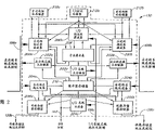
Fig. 2 is the block diagram of a preferred systems access controller.
Fig. 3 is the block diagram of a preferred correlativity wave filter and mark memory.
Fig. 4 is the block diagram of a preferred cache line address and preferred mark memory.
Fig. 5 A and 5B are the block diagrams of preferred buffer-manager.
Fig. 6 is the block diagram of a preferred central required list.
Fig. 7 is the block diagram of a preferred data-interface impact damper.
Fig. 8 is a process flow diagram, and expression has been addressed and keep the memory coherency method during the bus read command.
Fig. 9 is a process flow diagram, the preferred method that keeps memory coherency during bus invalidate command of expression.
Figure 10 is the dead queue block diagram in the another embodiment of the present invention.
In these figure, the first bit representation figure number of any 3 bit digital in the figure, these parts at first occur.For example, the parts that have a reference number 402 at first occur in Fig. 4.In addition, similarly reference number is used in whole accompanying drawing, the corresponding relation between the expression parts.
Embodiment
Preferred embodiment provides a kind of cache coherence, multiple bus system, this system 1) with multisystem bus and I/O bus and shared main storage interconnection, and 2) effectively keep cache coherence and reduce influence intrasystem stand-by period and total bandwidth.Especially, the present invention includes the correlativity wave filter, it adjusts bus-come to keep the cache memory correlativity with the little crossover bus traffic to-bus communication by this way.
Although the present invention is described with reference to preferred multiple bus system, the present invention is not only limited to this, and can be used in multiple other multibus contents.For the ease of fully understanding the present invention, lower part and fraction are formed in the prompting of detailed description:
I. vocabulary with the abbreviation index
II. preferred multiple bus system overview
I11. system's access controller
A. correlativity wave filter
1. mark memory
2. marking of control device
3. rotary encoder
4. rule list
B. buffer-manager
C. central required list
IV. data-interface impact damper
V. keep cache coherence
A. handle bus and read line command
B. handle bus and read to make capable invalid command
VI. other embodiment
VII. conclusion
I. vocabulary and the abbreviation index
The ASIC special IC.
The BRL order. bus is read line command.Bus is read the cache line on the line command read bus
The BRIL order. bus reads to make capable invalid command.Bus is read to make capable invalid command to read and is made the cache line on bus invalid.
The steering logic of the bus transaction that bus master controller (BusMaster) control is specific.In the system of some more than one equipment sharing of common bus, each equipment has internal logic to become bus master controller.After bus master controller was carried out bus transaction, bus master controller was abandoned bus so that another equipment can become bus master controller.This equipment comprises processor, I/O equipment.Memory Controller, or the like.
Bus slave (BusSlave) receives the steering logic of bus transaction from bus master controller.
Bus is inquired after (BusSnooping). a kind of technology that is used for monitoring the memory transaction of carrying out by other processor that makes by the processor that has cache memory
DIB. data-interface impact damper.
DEFER# signal .DEFER# signal delay bus transaction.In preferred PentiumPro bus, the DEFER# signal is not the coding of the control signal of a signal but the specific implication of sending the DEFER# signal.
DEN# signal .DEN# signal indicates when bus transaction can be delayed.Postponing bus transaction does not carry out in order.That is, if first bus transaction is delayed, then second bus transaction was done before first bus transaction that postpones.Whether the processor that sends bus transaction can postpone by the DEN# signal indication bus transaction of assert it.
FIFO. push-up storage.FIFO is a kind of memory array, its same order output project to be increased with project.That is, first project is advanced, and first project goes out.
The HIT# signal. in a preferred embodiment, each processor has the HIT# signal, and the HIT# signal is reached the standard grade in bus and connected together.Processor produces the HIT# signal and comes the designation data value for sharing.For example, when the first processor request msg value, the second processor controlling bus affairs also produce the HIT# signal, and at this moment second processor comprises the copy of requested data value.
The HITM# signal. in a preferred embodiment, each processor has the HITM# signal.When bus was inquired after data value of having revised of operation indication and is present in the cache memory, processor was assert the HITM# signal.
The I/O I/O. refer generally to the I/O affairs of input-output apparatus.
Pci bus. the peripheral component interconnect bus.
Processor (Processor). in whole detailed description, processor representation calculates or control assembly.Processor is by bus transaction and primary memory communication and can comprise cpu, microprocessor, and information equipment is handled or transmitted to the input-output apparatus of intelligence, and any other storage.
RAM. random access storage device,
SRAM. static random-access memory.
SDRAM. synchronous dynamic random access memory.
To inquire after and hit (SnoopHit). the cache memory of surveying it at processor occurs inquiring after when being included in the specific memory device affairs requested data and hits.
II. preferred multiple bus system overview
As shown in Figure 1, preferred multiple bus system 100 comprises three system buss: first system bus 102, second system bus 104 and tertiary system system bus 106.Each system bus 102,104 and 106 also comprises a group address and control row 108a, 108b and 108c, and one group of data line 110a, 110b and 110c.Address and control provisional capital are meant address and control row 108.What data line 110a, 110b and 110c referred to all is data line 110.In whole detailed description, first system bus 102 refers to that also bus 102, the second system buss 104 on the left side refer to the bus 104 on the right, and tertiary system system bus 106 refers to I/O bus 106.
In a preferred embodiment, each system bus 102,104 and 106 is the PentiumPro system bus, and it is specified by Intel Company.The PentiumPro system bus provides 36 address bits, 64 data bit and various control and error recovery signal.When preferred embodiment has been utilized the PentiumPro bus, those of ordinary skill in the art knows that the present invention is adapted to the system bus that cache coherency protocol is inquired after in realization on a large scale, and a kind of form of bus can be different from the form of another bus.
Be connected to the left side bus 102 be multiprocessor 112a and 112b, or the like.Be connected to the right bus 104 be multiprocessor 112c and 112d, or the like.Processor 112a, 112b, 112c and 112d refer to processor 112.In a preferred embodiment, each processor 112 has internally cached parts 114.Although 4 processors 112 are illustrated that each bus 102 and 104 can be connected to attached processor 112.Processor 112 in a preferred embodiment is the PentiumPro processor, is provided by Intel Company.Although the preferred embodiment of the invention has been utilized the PentiumPro processor, those of ordinary skill in the art knows, the present invention be adapted to can with the large-scale processor 112 of specific system bus compatibility.
Tertiary system system bus 106 is in a preferred embodiment transmitted I/O (I/O) affairs between a plurality of I/O bridges 120 and primary memory 132, therefore be known as I/O bus 106.Preferred I/O bridge 120 is 82450GXPCIsetOrionPCIBridge, is made by Intel Company.In a preferred embodiment, I/O bridge 120 uses pci bus to transmit the I/O affairs from I/O bus 106 and gives a plurality of I/O equipment 122.Yet those of ordinary skill in the art knows that I/O bridge 120 can be with providing the large-scale equipment to multiple I/O equipment 122 visits to realize.In addition, I/O bridge 120 can be selected for use, and compatible I/O equipment 122 can directly be received I/O bus 106.
Preferred multiple bus system 100 also comprises odd number main memory module 132a, even number main memory module 132b and data-interface impact damper 134.In a preferred embodiment, odd number main memory module 132a and even number main memory module 132b refer to primary memory 132.Preferred odd number memory module 132a and preferred even number memory module 132b comprise synchronous dynamic random access memory (SDRAM), and it can change to 32 kilomegabits from 32 megabits.SDRAM uses synchronous serial interface, and it provides high-speed data character string.
Preferred multiple bus system also comprises system's access controller 130 and data-interface impact damper 134.Say system's access controller control multiple bus system operation at large.System's access controller is coupled to address and control row 108a, 108b and 108c for each bus 102,104 and 106.In addition, system's access controller 130 also is coupled to one group of odd number memory address and controls row 138a, and row 140 is controlled with control row 138b and one group of data-interface impact damper (DIB) in one group of even number memory address.
On the other hand, data-interface impact damper 134 provides data routing to primary memory 132 between different bus 102,104 and 106.Data-interface impact damper 134 is coupled to data line 110a, 110b and 110c for each bus 102,104 and 106.In addition.Data-interface impact damper 134 is coupled to one group of main memory data capable 142.
Processor 112 is filled their cache memory 114 by read data from primary memory 132.In order in cache memory 114, to keep up-to-date data.Cache memory 114 in the processor 112 on specific bus is inquired after the main memory bus affairs on the distribution bus 102,104 or 106 that occurs in them.This is called as bus and inquires after.
When cache memory 114 comprises the cache line identical with the cache line that identifies in bus transaction, inquire after and hit generation.Hit when taking place when inquiring after, have data value and share the processor 112 or the processor 112 of copy and assert the HIT# signals.The HIT# signal is one of address and control row 108.Data that another processor 112 of HIT# signalisation is relevant with memory transaction and processor 112 are shared.In a preferred embodiment, if there are not other processors 112 to assert the HIT# signal, then the correlativity state of the data value of request handler setting requirement is occupied state.
In other cases, processor 112 can be revised the cache line in their cache memory 114.Yet in order to reduce bus traffic, cache memory 114 can not send the cache line revised to primary memory 132, asks same cache line up to another processor 112 from primary memory 132.For example, when processor 112 upgraded cache line, another processor 112 can not have the copy or the hope of cache line and obtain same cache line.In this case, the processor 112 with up-to-date cache line does not write back to primary memory 132 with up-to-date cache line.On the contrary, processor 112 keeps up-to-date cache line in its cache memory 114.
In a preferred embodiment, one of processor 112 is assert the HITM# signal, and at this moment bus is inquired after to operate and indicated a cache line of having revised to be present in the cache memory 114 of processor.The HITM# signal is that the processor 112 with up-to-date cache line of indicating in the lump of address and control row 108 need write back to cache line primary memory 132.For example, in a preferred embodiment, suppose that the first processor 112a on the bus 102 of on the left side comprises a cache line of having revised in its cache memory 114.When the second processor 112b on the bus 102 of on the left side wishes to obtain the copy of same cache line, the primary memory 132 execute store affairs of the bus 102 on the second processor 112b control left side and cache line that sign is required.Then, the first processor 112a inquires after memory transaction and determines that it comprises a version of having revised of the cache line of requirement.
In response, the first processor 112a assert its HITM# signal, and it comprises the version of having revised of a cache line indication of HITM# signal.The first processor 112a obtains the order of bus 102 on the left side and the cache line that will revise writes back to primary memory 132.After the cache line that the first processor 112a will revise write back to primary memory 132, the second processor 112b was again with the initialization of primary memory affairs and obtain up-to-date cache line.
Preferred processor 112 can represent whether bus transaction can postpone.Whether bus transaction can postpone to send its DEN# signal indication of processor 112 usefulness of bus transaction.Assert the response of HITM# Signal Processing machine control affairs.In case this processor is assert the HITM# signal, this processor or carry out bus transaction (completed) in order as storer, if perhaps affairs can postpone, then system's access controller 130 is assert the DEFER# signal that postpones bus transaction.The DEFER# signal is the coding of certain control row 108.
III.
System's access controller
Now, system's access controller 130, as shown in Figure 2, preferred systems access controller 130 is special IC (ASIC).Say at large, when in multiple bus system 100, keeping cache coherence, system's access controller three buses 102,104 of 130 controls and 106 and primary memory 132.
The most preferably, system address controller 130 comprises the correlativity wave filter 200a on the left side, the correlativity wave filter 200b and the I/O correlativity wave filter 200c on the right.In whole detailed description, the correlativity wave filter 200a on the left side, the correlativity wave filter 200b on the right and I/O correlativity wave filter 200c refer to correlativity wave filter 200.System's access controller 130 also comprises the bus master controller 202a on the left side, the bus master controller 202b and the I/O bus master controller 202c on the right.In whole this detailed description, the bus master controller 202a on the left side, the bus master controller 202b on the right and I/O bus master controller 202c refer to bus master controller 202.
In addition, system's access controller 130 comprises the bus slave 204a on the left side, the bus slave 204b and the I/O bus slave 204c on the right.In whole detailed description, the bus slave 204a on the left side, the bus slave 204b on the right and I/O bus slave 204c refer to bus slave 204.And system's access controller 130 comprises odd number memory controller 206a and even number memory controller 206b.In whole detailed description, odd number memory controller 206a and even number memory controller 206b refer to Memory Controller 206.
System's access controller 130 also comprises central required list 208 and buffer-manager 210.At last, system's access controller 130 is coupled to the mark memory 212a on the outside left side, the mark memory 212b and the inner I/O mark memory 212c on outside the right.In whole detailed description, the mark memory 212a on the left side, the mark memory 212b on the right and I/O mark memory 212c be digit synbol storer 212.
In a preferred embodiment, the bus slave 204a on the bus master controller 202a on the correlativity wave filter 200a on the mark memory 212a on the left side, the left side, the left side and the left side distributes to the bus 102 on the left side.The bus master controller 202b on the mark memory 212b on the right, the correlativity wave filter 200b on the right, the right and the bus slave 204b on the right distribute to the bus 104 on the right.I/O mark memory 212c, I/O correlativity wave filter 200c, I/O bus master controller 202c and I/O bus slave 204c distribute to I/O bus 106.
Now, interconnection in system's access controller 130, the correlativity wave filter 200a on the left side is with the bus address on the left side and control row 108a, the mark memory 212a on the left side, mark memory 212b, I/O mark memory 212c, buffer-manager 210 and the central required list 208 on the right communicated by letter.The correlativity wave filter 200b on the right is with the bus address on the right and control row 108b, the mark memory 212a on the left side, mark memory 212b, I/O mark memory 212c, buffer-manager 210 and the central required list 208 on the right communicated by letter.I/O correlativity wave filter 200c is with the I/O bus address and control row 108c, the mark memory 212a on the left side, mark memory 212b, I/O mark memory 212c, buffer-manager 210 and the central required list 208 on the right communicated by letter.
The bus master controller 202a on the left side communicates by letter with central required list 208 with the bus address on the left side and control row 108a.The bus master controller 202b on the right communicates by letter with central required list 208 with the bus address on the right and control row 108b.I/O bus master controller 202c communicates by letter with central required list 208 with I/O bus address and control row 108c.
The bus slave 204a on the left side is with the bus address on the left side and control row 108a, odd number memory controller 206a, even number memory controller 206b communicates by letter with buffer-manager 210.The bus slave 204b on the right communicates by letter with buffer-manager 210 with control row 108b, odd number memory controller 206a, even number memory controller 206b with the bus address on the right.I/O bus slave 204c is with the I/O bus address and control row 108c, odd number memory controller 206a, even number memory controller 206b communicates by letter with buffer-manager 210.
Therefore, central required list is communicated by letter with I/O bus master controller 202c with correlativity wave filter 200a, correlativity wave filter 200b, the I/O correlativity wave filter 200c on the right, the bus master controller 202a on the left side, the bus master controller 202b on the right on the left side.Buffer-manager 210 is communicated by letter with correlativity wave filter 200a, correlativity wave filter 200b, the I/O correlativity wave filter 200c on the right, the bus master controller 202a on the left side, bus master controller 202b, the I/O bus master controller 202c on the right, the bus slave 204a on the left side, bus slave 204b, I/O bus slave 204c, odd number memory controller 206a and the even number memory controller 206b on the right on the left side.
Now, bus master controller 202.Bus master controller 202 is controlled at the bus transaction on their bus that is assigned with 102,104 and 106.For example, the bus transaction on the bus 102 of the bus master controller 202a initialization on the left side on the left side.After bus master controller 202 one of execution or more bus transaction, bus master controller 202 is abandoned bus so that another equipment can become bus master controller.Be used for realizing that the steering logic of controller 202 is that those skilled in the art is known.
Now, bus slave 204, bus slave 204 receives by a processor 112 or I/O bridge 120 initialized bus transaction on their distribution bus 102,104 and 106.For example, this processor 112 is that a specific data value in the primary memory 132 can initialization read bus affairs.Bus slave 204 receives bus transaction and obtain requested data value from primary memory 132.The steering logic that realizes bus slave 204 is that those skilled in the art is known.
Odd number memory controller 206a and even number memory controller 206b control the visit to odd number main memory module 132a and even number main memory module 132b respectively.Odd number memory controller 206a and even number memory controller 206b use storage controlling technology control odd number main memory module 132a well-known to those having ordinary skill in the art and even number main memory module 132b.
A. correlativity wave filter
Now, preferred correlativity wave filter 200.Each correlativity wave filter 200 determines that what bus transaction or bus transaction group must keep cache coherence.In a preferred embodiment, in multiple bus system 200, when the unnecessary maintenance cache coherence of crossover bus affairs, each correlativity wave filter 200 improves performance by the restriction crossover bus traffic.
As described above, the bus address on the correlativity wave filter 200a monitoring left side on the left side and control row 108a, the bus address on the correlativity wave filter 200b monitoring the right on the right and control row 108b, I/O correlativity wave filter 200c monitoring I/O address and control row 108c.As shown in Figure 3, each correlativity wave filter 200 comprises marking of control device 300, rotary encoder 302 and rule list 304.In addition, each correlativity wave filter 200 is assigned to one of mark memory 212.
1. mark memory.
More preferably, each mark memory 212 is stored in the static random-access memory (SRAM) that is positioned at system's access controller 130 outsides.The mark memory 212a on the left side and the mark memory 212b on the right are preferably same length and the I/O mark memory is less on length, and this is because generally be coupled to the very little cache portion of I/O bridge 120 grades.The mark memory 212 of distributing to specific bus keeps these superset records: the cached state of the cache line cache line and 2 that 1) is arranged in the cache memory 114 that is connected with distribution bus).In a preferred embodiment, cached state represents that with one group of cache coherence state cached state comprises less state than the cache coherence state in the cache memory 114.
As everyone knows, each cache line in the primary memory identifies with cache line address.The length of cache line all changes to another multiple bus system 100 from a multiple bus system 100.In a preferred embodiment, cache line comprises 32 8 bit data value (256).Each mark memory 212 storaging mark cache line is not the cache line address of actual cache line.Except that storage cache line address, each mark memory 212 is also stored the correlativity state information relevant with cache line address.Like this, the information of each mark memory 212 maintenance is as the possible content and the state that are stored in the cached data of the cache memory 114 that is connected with the distribution bus of mark memory.
For example, when the processor 112a on the bus 102 of on the left side produced the read bus affairs of the cache line in the visit primary memory 132, this processor 112a placed on the bus address and control row 108a of the cache line address on the left side that requires.As described in more detail below, storage cache line address among the cache line address that the correlativity wave filter 200a reception on the left side requires and the mark memory 212a of on the left side.In addition, the storage correlativity state relevant among the mark memory 212a of the correlativity wave filter 200a on the left side on the left side with cache line address.
The correlativity state relevant with each cache line address relates to the state of the cache line in the cache memory 114.In a preferred embodiment, the correlativity state comprises three different correlativity states: disarmed state, shared state or occupied state.Disarmed state represents that cache line is invalid, and processor 112 can not use it.Shared state represents that processor 112 can not revise cache line.For example, the shared cache line is the programmed instruction that is not modified often.Occupied state representation cache line can be occupied the processor 112 of cache line to be revised.Preferred embodiment has been utilized invalid, shares and occupied agreement, is because it is adapted to comprise on a large scale the cache coherency protocol of the MESI agreement of being utilized by PentiumPro processor 112.
Yet those of ordinary skill in the art knows that it is invalid that the correlativity state of cache line is not limited to, and shares and occupied agreement.In fact, those of ordinary skill in the art knows, the correlativity state may be realized with a large-scale coherency protocol, as that revised, that monopolize, shared and invalid (MESI) agreement, that revised, occupied, that monopolize, shared and invalid (MOESI) agreement, that revised, shared and invalid (MSI) agreement, Berkeley agreement, the UniversityofIllinois coherency protocol, perhaps other etc.
The correlativity state also may be realized as an invalid and occupied agreement of two condition with the two condition coherency protocol.At double bus system, in the two condition coherency protocol, all buses are considered to have the shared copy of all cache lines.This reduces the length of correlativity storer often, because be seen as when sharing when all cache lines, the correlativity storer only needs the record that keeps relevant with the data value that is in invalid and occupied state.Advantageously, when bus is a shared data when carrying out a standard and reading affairs, shared state information can not be stored in the correlativity storer.This reduced with keep the correlativity storer in the relevant problem of correlativity state information superset.
Yet in this two condition system, all special uses are read affairs or invalidation transactions and are required one or more crossover bus affairs to guarantee cache coherence.This crossover bus affairs must see whether in fact another bus comprises the shared vision of reading the relevant data of affairs with the special use of invalid command.And in double bus system, a two condition agreement can cause higher overall performance, utilizes two above buses, and the benefit of two condition agreement is the characteristic that greatly depends on working load.
Preferred PentiumPro processor 112 is not exported accurately the correlativity state information about the cache line in the internal cache 114 that is stored in them.For example, internal cache 114 can be discarded unmodified cache line and not send the signal that this cache line has gone out of use.In the preferred embodiment of the invention, each mark memory 212 is adapted to guarantee cache coherence for the internal cache 114 of not exporting current correlativity state information uniquely.
Each mark memory 212 guarantees cache coherence by the superset that keeps a cache line address, and cache line address may current being kept in the internal cache 114 that is connected with specific bus.For example, the mark memory 212 on the left side keeps a cache line address superset, and cache line address may be kept in processor 112a and the processor 112b internal cache 114.Because the unnecessary flag state information accurately that comprises of cache line address superset is when the in fact discarded cache line tense marker storer 212 of cache memory 114 can represent that cache line specific in the cache memory 114 is in shared state.In other cases, when cache memory 114, in fact.When giving primary memory 132 with the cache line write-back, the superset of the cache line address in the mark memory 212 can represent that cache line specific in the cache memory 114 is in the state of having revised.
In order to keep a cache line address superset, preferred mark memory 212 uses the rule that contains that is known as.Contain the regular cache line address that guarantees to be stored in the cache memory 114 that is connected with specific bus and always distribute to the subclass of the cache line address in the mark memory 212 of that bus.When cache line address is deleted from a mark memory 212, contain the relevant cache memory 114 of rule indication so that the cache line in their cache memory is invalid.
For example, when the mark memory 212a on the left side does not have memory span to preserve new cache line address, must prepare the space among the mark memory 212a of on the left side new cache line address by from the mark memory 212 on the left side, getting rid of an existing cache line address (old cache line address).If old cache line address is in disarmed state (cache memory 114 that connects with bus does not re-use the cache line relevant with old high-speed cache address), the correlativity wave filter 200a on the left side replaces old cache line address with new cache line address simply.
Yet, when old cache line address is in shared or occupied state, the correlativity wave filter 200a on the left side can not get rid of old cache line address from the mark memory 212a on the left side, make old cache line address invalid up to cache memory 114.As mentioned above, the mark memory 212a on the left side with cache memory 114 that the bus 102 on the left side is connected in must keep a cache line address superset, like this, the mark memory 212a of on the left side can replace before the old cache line address with new cache line address, and old cache line address must at first be disabled in cache memory 114.
As described in more detail below, the correlativity wave filter 200a on the left side makes the old cache line address in the cache memory 114 that is connected with the bus 102 on the left side invalid by carrying out the invalidation bus affairs.The invalidation bus affairs occur on the bus on the left side, and the bus on left side indication cache memory 114 internally makes old cache line address invalid.
Yet under certain conditions, old cache line can be in occupied state and a cache memory 114 can be revised old cache line.If cache memory 114 may be revised old cache line, bus reads to make invalid being performed of row (BRIL) affairs.If cache memory 114 has been revised old cache line, then read to make to act in bus and be engaged between dynamic stage, cache memory 114 is got the order of bus transaction and will be write back to primary memory 132 corresponding to the cache line of having revised of old cache line address.The cache line of having revised is write back to after the primary memory, and the correlativity wave filter 200a on the left side replaces old cache line address among the mark memory 212a on the left side with new cache line address.Like this, in order to keep the superset of a cache line address in mark memory 212, under certain conditions, before old cache line can be replaced, the data that cache memory 114 must will have been revised write back to primary memory 132.
The form of cache line address 400 and each mark memory 212 is shown among Fig. 4.Cache line address 400 is divided into two parts from conceptive.First comprises flag page address 402, and second portion comprises displacement address 404.In a preferred embodiment, the 410 number definition of the inlet of the mark in the mark memory 212 are called as the length of flag page.More preferably, each mark memory 212 has the number of mark inlet 410, and like this, they have same flag page length.
In a preferred embodiment, flag page address 402 signs comprise the flag page of cache line address 400, and the position of the cache line address 400 in the displacement address 404 identity marking pages or leaves.Especially.High-order identity marking page address in the cache line address 400 and its low level sign displacement address 404.
In general, low level is known as index, because the position of the cache line address in the low level identity marking page or leaf.For example, for first cache line address 400, the position of the high-speed cache address line 400 in upper address bits identity marking page address 402 and the low address bit-identify flag page.
Because flag page can change on length, the figure place of distributing to flag page address 402 and displacement address 404 also changes.In a preferred embodiment, if the mark memory 212b on the mark memory 212a on the left side and the right comprises 216 inlets, displacement address 404 comprises the lower 16 of cache line address 400 so, and flag page address 402 comprises higher 15 of cache line address 400.As mentioned above, I/O mark memory 212c is less on length, thereby comprises less inlet.In a preferred embodiment, I/O mark memory 212 comprises 32 inlets.
The different length of following expression meaning mark memory 212 and the length of respective markers page address 402 in the cache line address 400 and displacement address 404.
| Mark memory length | The flag page address width | The |
| 2 16Individual inlet | 15 | 16 |
| 2 17Individual inlet | 14 | 17 |
| 2 18Individual inlet | 13 | 18 |
| 2 19Individual inlet | 12 | 19 |
In a preferred embodiment, correlativity wave filter 200 uses direct mapping technique storage cache line address 400 in mark memory 200.Directly each cache line address 400 map to of map representation specific markers enters the mouth 410.Fig. 4 illustrates preferred mark memory 212, and it comprises 2
16Individual mark inlet 410.Each mark inlet 410 comprises the flag page address 402 of cache line address 400.In addition, each mark inlet 410 comprises correlativity state position 412 and parity bits 414.Parity bits 414 provides known parity error to detect.
When processor 112 access cache line addresses 400, correlativity wave filter 200 uses displacement address 404 to identify specific markers inlet 410.Correlativity wave filter 200 then storage mark page address 402 in the mark inlet 410 of mark.For example, when the first processor 112a on the bus 102 of on the left side visited first cache line address 400 in first flag page, the correlativity wave filter 200a on the left side used cache line displacement address 404 to locate first mark inlet 410 among the mark memory 212a on the left side.The correlativity wave filter 212a on left side storage mark page address 402 then enters the mouth 410 to first mark among the mark memory 212a on the left side.
Except that the flag page address 402 of storage cache line address 400, mark inlet 410 also gives cache line address 400 storages one group of correlativity state position 412.More preferably, the correlativity state position 412 in the mark inlet 410 comprises preferred three correlativity states: disarmed state, shared state or occupied state.Three correlativity states are represented with two correlativity state positions 412.Following table definition is distributed to the correlativity state of correlativity state position 412.
| Correlativity state position | The correlativity state |
| 00 | Invalid |
| 01 | Share |
| 10 | Occupied |
| 11 | (reservation) |
2. marking of control device
Directly mapping cache line address 400 is arranged in marking of control device 300 to the steering logic of mark memory 212.The marking of control device 300 of distributing to the bus 102 on the left side is called the marking of control device 300a on the left side.The marking of control device 300 of distributing to the bus 104 on the right is called the marking of control device 300b on the right.The marking of control device 300 of distributing to I/O bus 106 is called I/O marking of control device 300c.For example, the marking of control device 300 on the left side comprises direct map logic, and directly the direct mapping cache line of map logic address 400 is in the mark memory 212a on the left side.
Steering logic in the marking of control device 300 is similar to and is used to the steering logic of direct mapping cache line in the cache memory 114.Like this, marking of control device 300 uses the direct map logic that those those skilled in the art know.Yet this is different from the high-speed cache steering logic in the preferred PentiumPr0 processor 112, and preferred PentiumPr0 processor 112 utilizes the four-way group mapping technique of being correlated with.
As described in more detail below, correlativity wave filter 200 partly determines whether to carry out the crossover bus affairs according to the correlativity state information in the mark memory 212.In a preferred embodiment, each marking of control device 300 also is coupled to its mark memory 212 and the mark memory 212 of distributing to other buses.Mark in each marking of control device 300 can access flag storeies 212 enters the mouth 410 the time, and the mark that each marking of control device 300 is only revised in its own mark memory 212 that distributes enters the mouth.For example, the marking of control device 300a on the left side can visit the mark memory 212b and the inlet of the mark among the I/O mark memory 212c 410 on mark memory 212a, the right on the left side, but the marking of control device 300 on the left side is only revised the mark inlet 410 among the mark memory 212a on the left side.
For example, when the bus 102 on the left side was specific cache line address 400 transfer bus affairs, the marking of control device 300a on the left side used cache line address 400 to obtain corresponding correlativity state position 412 from the mark memory 212a on the right and I/O mark memory 212b.In this example, cache line address 400 is directly by mark memory 212b the correlativity state position to obtain on the right of of map to the right.In addition, cache line address directly by map to I/O mark memory 212c to obtain I/O correlativity state position 412.In whole detailed description, the correlativity state position 412 that obtains from another mark memory 212 of distributing to other buses is taken as Long-Range Correlation mode bit 412.In case the marking of control device 300a on the left side obtains Long-Range Correlation mode bit 412, the marking of control device 300a on the left side transmits Long-Range Correlation mode bit 412 with regard to forward and gives rotary encoder 302.
3. rotary encoder
Each rotary encoder 302 determines that any bus transaction is just occurring on one of bus 102,104 or 106.Distribute the rotary encoder 302 of the bus 102 monitor the left side to be called as the rotary encoder 302a on the left side.The rotary encoder 302 of the bus 104 on the right of distribution is monitored is called as the rotary encoder 302b on the right.Distribute the rotary encoder 302 of monitoring I/O bus 102 to be called as I/O rotary encoder 302c.Like this, the address that 302 monitoring of each rotary encoder are relevant with its distribution bus 102,104 or 106 and control row 108.
More preferably, rotary encoder 302 use be applied to bus 102,104 and 106 on the relevant known techniques of specific bus protocol, come controlling bus control row, so that determine whether bus transaction read data or give primary memory 132 write datas from primary memory 132.In a preferred embodiment, rotary encoder 302 uses known technology to determine just reading of data or data are write in the primary memory 132 from primary memory 132 of which PentiumPr0 bus transaction.In case rotary encoder 302 determines to occur in the type of the bus transaction on its distribution bus, rotary encoder 302 is given rule list 304 with regard to transfer bus round-robin type.
4. rule list
Now, be illustrated in the rule list 304 among Fig. 3, rule list determines when that carrying out the crossover bus affairs guarantees cache coherence.In a preferred embodiment, the rule list 304 of distributing to the bus 102 on the left side is called the rule list 304a on the left side.The rule list 304 of distributing to the bus 102 on the right is called the rule list 304b on the right.The rule list 304 of distributing to the I/O bus is called I/O rule list 304c.
The Long-Range Correlation mode bit 412 that each rule list 304 is estimated the bus transaction type information and obtained from rotary encoder 302.In a preferred embodiment, each rule list 304 is big truth tables, is arranged in static random-access memory (SRAM).Being stored in each rule list memory location, is need be performed with the crossover bus affairs that guarantee cache coherence and the type of local bus transaction.
In addition, rule list 304 is carried out and is inquired after action.In a preferred embodiment, when the global flag storer represented that they have the shared copy of cache line, rule list 304 can be assert the HIT# signal.Assert that HIT# signal indication on remote bus or more cache memory have the shared copy of cache line.Rule list 304 can assert that also the HIT# signal does not produce the crossover bus traffic code is read affairs and be set as shared state by force so that the code in future on another bus is read affairs.
The specific crossover bus transaction code that must guarantee cache coherence is enclosed in the rule list 304 under the control of system's access controller 130.Preferred multiple bus system 100 is loaded into rule list 304 with the crossover bus transaction code during the initialization of system.Because the crossover bus transaction code can be modified, so the crossover bus affairs can be adjusted effectively to different multiple bus system 100.
B. buffer-manager
Buffer-manager 210, central required list 208 and data-interface impact damper 134 are illustrated in Fig. 1 and 2, optimize communication between multibus.In a preferred embodiment, central required list 208, buffer-manager 210 and data-interface impact damper 134 comprise the multiport pond of memory cell (not shown), and they can be by all buses 102,104 and 106 visits.Advantageously, any bus 102,104 or 106 can be read or writes to any other bus 102,104 or 106 and do not use the separate connection path from any other bus 102,104 or 106.
In a preferred embodiment, the information relevant with each bus transaction is subdivided into three parts, and they are stored in three different memory cells, the address location that promptly is known as, request unit and data cell.Therefore.One-to-one relationship is present in each data cell, between each request unit and each address location.As described in more detail below, address location is positioned at buffer-manager 210, and request unit is positioned at central required list 208 and data cell is positioned at data-interface impact damper 134.
Preferred buffer-manager 210 is illustrated in Fig. 5 A and 5B.See Fig. 5 A, buffer-manager 210 comprises the pond of the FIFO506c on first in first out (FIFO) storer 506a, the I/OFIFO506b on address location 500, address location priority encoder 504, the left side and the right.Each address location 500 is a multiport, and communicates by letter with address location priority encoder 504, bus master controller 202, bus slave 204, Memory Controller 206 and the comparer 510 that is illustrated in Fig. 5 B.
Preferred buffer-manager 210 comprises 64 address locations 500.Shown in Fig. 5 A, each address location 500 comprise one "-use " position 502, storage address 504 and one group of data cell mode bit 505.-use the position specific address location 500 of 502 expressions whether can use.In a preferred embodiment ,-use position 502 to be set to represent whether address location 500 is in uses or idle condition.Storage address 504 comprises storage address 504, and the type of data cell mode bit 505 expression bus transaction.Especially, whether data cell mode bit 505 expression invalidation bus affairs will be performed.
Now, address location priority encoder 504, address location priority encoder 504 determines which address location 500 is using, which address location 500 is idle to receive new bus transaction information.In a preferred embodiment, the logic in the address location priority encoder 504 by estimate in each address location 500-use position 502 to determine which address location 500 is the free time.If-use position 502 to set, then address location 500 is using.If-use position 502 not set, then address location is idle.Free cells is selected in a looping fashion.
Address location priority encoder 504 determines that not only which address location 500 is idle, and distributes idle address location 500 to give different buses 102,104 and 106.More preferably, address location priority encoder 504 distributes idle address location 500 to give different buses 102,104 and 106 with a kind of recycle design.As described in more detail below, when bus transaction information is stored in idle address location 500 ,-to use position 502 to be set presentation address unit 500 be not idle.
For example, suppose the first, the second and three-address unit 500 be idle.Preferred priority encoder 504 definite the first, the second and three-address unit 500 are idle, and distribute first address location 500 to give I/O bus 106 for bus 104, the three-address unit 500 on the right for bus 102, the second address locations 500 on the left side.When four-address unit 500 became the free time, address location priority encoder 504 was circulated back to the bus 102 on the left side, and the bus 500 of distributing four-address unit 500 to give the left side.When preferred address location priority encoder 504 distributed idle address location to give different buses, those skilled in the art were appreciated that address location priority encoder 504 can utilize large-scale allocation model to distribute idle address location 500 to give different buses 102,104 and 106.
Now, FIFO storer 506 in the buffer-manager, the address location identifier of the address location 500 that FIFO storer 506 interim storaging marks are assigned with, the address location identifier is a data variable, it comprises the memory location of the address location 500 that is assigned with.In a preferred embodiment, 64 address locations 504 of address location identifier sign.Address location memory location as described in more detail below, that bus master controller 202 uses the address location identifier in the FIFO storer 506 to be identified by the address location identifier with visit.
In a preferred embodiment, each FIFO storer 506 is to bus slave 204 and 200 outputs of correlativity wave filter.Like this, the FIFO storer 506a on the left side is to the bus slave 204a on the left side and the correlativity wave filter 200a output on the left side.The FIFO storer 506b on the right is to the bus slave 204b on the right and the correlativity wave filter 200b output on the right.I/OFIFO storer 506c is to I/O bus slave 204c and I/O correlativity wave filter 200c output.When one of one of bus slave 204 or correlativity wave filter 200 wished to send a bus transaction to another bus, they obtained an address location identifier from the FIFO storer 506 that they are assigned with.
Like this, preferred buffer-manager 210 provides the pond with all buses 102,104 and 106 address locations 500 that interconnect, and the pond of this address location 500 rather than independently total thread path are provided, and has reduced system complexity.And address location priority encoder 504 and FIFO storer 506 guarantee that idle address location 500 even distribution are between bus 102,104 and 106.
In another aspect of the present invention, shown in Fig. 5 B, preferred buffer-manager 210 comprises the address comparator 510 of a plurality of home addresses conflict, and in general, when two different bus transaction related to same data value and take place simultaneously, address conflict produced.In this case, two different bus transaction that may occur in 500 pairs of address locations 500 of two address locations comprise same storage address 504.In this case, incorrect bus transaction may take place.
When a bus slave 204 received bus transaction, bus slave 204 forwards transmitted the address relevant with bus transaction to the address comparator 510 of distributing to the bus identical with bus slave 204.The newer storage address 504 of address comparator 510 with all be present in-use the storage address 504 of address location 500.If same storage address-use in the address location 500 and found, address comparator 510 produces output, these output notice bus slave 204 address conflicts exist.Bus slave 204 sends the retry signal then to making the initialized processor 112 of bus transaction that produces address conflict.Processor 112 is then in initialization bus affairs later.
In a preferred embodiment, a group address comparer 510 is distributed to each bus.Like this, the address comparator 510a set of dispense on the left side is given the bus 102 on the left side.The address comparator 510c set of dispense on the right gives I/O bus 106 for the bus 104 on the right and I/O address comparer 510a set of dispense.When bus slave 204 received new storage address 504, bus slave 204 forwards transmitted new storage address 504 and give address comparator 510.Address comparator 501 estimate then be present in-use storage address 504 in the address location 500 to determine whether address conflict exists.
For example, the bus slave 202b on the right can receive a kind of I/O affairs, and this affairs are transmitted to an I/O bridge 120 on I/O bus 106.For receiving the storage address relevant with the I/O affairs, the bus slave 202b forward on the right transmits the address comparator 510c that this storage address is given the right.The address comparator 510c on the right is this storage address and existing storage address 504 in-use address location 500 relatively.If the copy of this storage address be present in-use in the address location 500, address comparator then sends the bus slave 202b of a signal to the right, presentation address conflict existence.In this example, the bus slave 202b on the right indication processor 112c or 112d are with in retry I/O affairs later.
When carrying out the invalidation bus affairs, when making an inlet of mark memory 212 invalid, wish to postpone invalid operation when later bus is not in a hurry.A kind of method is the old cache line address (with the cache line address that is disabled) of storage in buffer-manager.In a preferred embodiment, the address location 500 in the buffer-manager 210 comprises the whole storage address of a cache line, and cache line comprises flag page address 402 relevant with cache line and displacement address 404.Increase old cache line address and allow multiple bus system 100 to proceed new bus transaction for an address location 500, although in fact old cache line address also is not disabled.
Suppose that another bus transaction relates to the old cache line address 400 that is present in the buffer-manager 210, when bus transaction was received by a bus slave 204, bus slave 204 forwards transmitted the address relevant with bus transaction and give address comparator 510.The displacement address 404 of displacement address 404 that address comparator 510 comparisons are relevant with bus transaction and old cache line address.If any address conflict exists, then comparer evaluating data location mode position 505.If the old cache line address of data cell state 505 expressions need be disabled, so new bus transaction is forced to retry, can be disabled up to old cache line address 400.Illustrate in another embodiment of this method part that is entitled as " other embodiment " below
C. central required list
Now, preferred central required list 208 is illustrated in Fig. 6, and central required list 208 comprises request unit 600, the bus priority scrambler 602a on the left side, the pond of the bus priority scrambler 602b on the right and I/O bus priority scrambler 602c.Each request unit 600 is multiport and communicates by letter with each address location priority encoder 602.In preferred central required list 208,64 request units 600 are arranged.And one-to-one relationship is present between 64 address locations 500 and 64 request units 600.
Each request unit 600 comprises target bus identifier 604, bus transaction code 606 and occupant's bus identifier 608.Target bus identifier 604 recognition purpose buses 102,104 or 106.As described in more detail below, the not scheduled justice of bus identifier 604, on the contrary, preferred embodiment is set the bus 102 that bus identifier 604 identifies the right, the bus 104 on the left side or I/O bus 106.For example, the bus 104 that target bus identifier 604 can specify bus transaction code 606 to give the right, on the other hand, the type of the bus transaction of bus transaction marking code on the purpose bus is to carry out.In a preferred embodiment, bus master controller 202 is carried out the bus transaction that is identified by bus transaction code 606.Occupant's bus identifier 608 identifies the bus of making a start.For example, occupant's bus identifier 604 can be indicated the bus transaction code 606 of making a start on the bus 102 of on the left side.
The target bus identifier 604 that the bus priority scrambler is estimated in each request unit 600 is specified different buses to determine which request unit.The bus master controller 202 relevant with one of bus 102,104 or 106 carried out the bus transaction that is identified then in specific request unit 600.For example, the bus priority scrambler 602a on the left side estimates all target bus identifiers 604 to identify the bus 102 which request unit 600 is given the left side.The bus priority scrambler 602b on the right estimates all target bus identifiers 604 to identify the bus 104 which request unit 600 is given the right.I/O bus priority scrambler 602c estimates all target bus identifiers 604 and gives I/O bus 106 to identify which request unit 600.
Except that recognition purpose bus 102,104 and 106, each bus priority scrambler 602 determines that also which bus request unit 500 relevant with specific bus 102,104 or 106 has limit priority.In a preferred embodiment, each bus priority scrambler 602 uses circle logic to determine highest priority request unit 600.In case each bus priority scrambler 602 forward transmits the distribution bus that it is given in highest priority request unit 600, each bus priority scrambler 602 is given each request unit 600 with regard to cycle assignment priority.Circle logic guarantee each bus priority scrambler 602 in turn assigned highest priority give all bus request unit 600.This circle logic is known for those those of ordinary skill in the art.
For example, the bus priority scrambler 602b that supposes the right has identified the bus 104 that two request units 600 are given the right.The bus priority scrambler 602b on the right distributes first request unit, 600 limit priorities and sends the bus master controller 202b of the first request unit identifier to the right.The bus priority scrambler 602b on the right distributes second request unit, 600 limit priorities then and sends the bus master controller 202b of the second request unit identifier to the right.When the bus priority scrambler 602b on the right arrived the end mark of request unit 600 of the bus 104 of distributing to the right, the bus priority scrambler on the right turned back to the beginning in the pond of request unit 500.
Like this, central required list 208 provides a pond with the request units 600 of all bus 102,104 and 106 interconnection.This request unit 600 ponds, when contrasting with the independent bus line access path, it can reduce system complexity.And the bus transaction in bus priority scrambler 602 each request unit of assurance in the central required list 208 is carried out by bus 102,104 and 106.
IV. data-interface impact damper
Now, preferred data-interface impact damper 134, as shown in Figure 7, data-interface impact damper 134 comprises 700 ponds, a data unit, and control and index mechanism 702.Each request unit 600 for multiport and with data line 110a, 110b and 110c and be connected to odd number main memory module 132a and communicate by letter with 142b with data line 142a on the even number main memory module 132b.In preferred central required list 208,64 data unit 700 are arranged.And correspondence is present between 700,64 request units 600 in 64 data unit and 64 address locations 500 one by one.Each data cell 700 comprises a data value relevant with bus transaction.
Control and index mechanism 702 receive DIB control row 140 from bus slave 204.Specific data cell 700 and one of bus 102,104 or 106 of DIB control row 140 signs.For example, when I/O bus slave 204 increased new bus transaction to an address location 500 and a request unit 600, I/O bus slave 204 also increased the data relevant with new bus transaction and gives corresponding data cell 700.In this example, I/O bus slave 204 assert that DIB control row is with sign inherent data unit 700.Control and index mechanism 702 make inherent data unit 700 receive data from I/O data line 110c then.
Like this, the data-interface impact damper provides can be provided this data cell 700 ponds rather than bus interconnection independently by data cell 700 ponds of all buses 102,104 or 106 visits, has reduced system complexity and has improved performance.
V. keep cache coherence
Bus transaction by 200 monitoring of correlativity wave filter comprises that bus is read line command and bus reads to make capable invalid command.Bus is read the cache line of row (BRL) order reading command code or data from primary memory 132 and is made it invalid.Bus reads to make row invalid (BRIL) order to make cache line invalid.Although when preferred rule list 304 was adapted to these bus line commands, those of ordinary skill in the art knew that rule list 304 can be adapted to many different bus line commands, and is not limited to the bus line command of preferred embodiment.
A. handle bus and read line command
Fig. 8 illustrates to the figure shows maintenance cache coherence when one of bus 102,104 or 106 execution bus is read row (BRL) order by a process flow diagram.Carry out the BRL order from 800, one processors of begin block 112.During the BRL command execution, processor 112 sends correlativity wave filter 200 and the bus slave 204 of the cache line address 400 of the cache line that requires to its distribution.
When bus slave 204 received cache line address, bus slave 204 forwards transmitted cache line address and give the address comparator 510 of distributing to same bus.Address comparator 510 relatively this displacement address 404 and be present in-use the displacement portion of the storage address 504 of address location 500 any address conflict of assigning to determine whether to exist.Whether address comparator 510 also evaluating data location mode position 505 relates to invalidation transactions with the address location 500 of determining the generation address conflict.If like this, address comparator 510 sends the address conflict signal to bus slave 204.Bus slave 204 then indication request processor 112a with in the order of retry BRL later.
If address comparator does not indicate address conflict to exist, then preferred embodiment is proceeded piece 802, and rotary encoder 302 is determined bus 102,104 or 106 execution BRL orders.And the marking of control device 300 of distributing to bus 102,104 or 106 uses the cache line address 400 of sign in the BRL order to visit the cache line address 400 in the mark memory 212 (global flag storer 212) of distributing to other buses 102,104 and 106.Global flag storer 212 returns Long-Range Correlation mode bit 412, and whether its indication remote cache line address 400 is in disarmed state, shared state or occupied state.
Have only a global flag storer 212 can comprise the specific cache line address that is in occupied state.Yet a more than global flag storer 212 can comprise the specific cache line address that is in shared or invalid state.Another global flag storer 300 comprises the copy of the same cache line address that is in disarmed state if global flag storer 212 comprises the copy of the cache line address that is in shared state, and the correlativity state position 412 that is in shared state is preferential.As described in more detail below, if a more than global flag storer 300 comprises the copy of the specific cache line address that is in shared state, then association rules 304 can be carried out remote bus affairs on a more than remote bus 102,104 or 106 to guarantee cache coherence.In addition, if neither one comprises specific cache line address 400 in the global flag storer 300, relevant with cache line address 400 so Long-Range Correlation mode bit 412 considered to be in disarmed state.
For example, when the first processor 112a on the bus 102 of on the left side is a cache line address specific in the piece 802 400 when producing the BRL order, the rotary encoder 302a on the left side determines that the bus on the left side carries out the BRL order.And the marking of control device 300 on the left side uses mark memory 212b and the remote I/O mark memory 212c of cache line address 400 to visit long-range the right.Marking of control device 300 obtains Long-Range Correlation mode bit 412 from the mark memory 212b on the right and I/O mark memory 212c, whether the mark memory 212b on Long-Range Correlation mode bit 412 expression the right and the cache line address 400 among the I/O mark memory 212c are in disarmed state, shared state or occupied state.If neither the mark memory 212b on the right neither comprise cache line address 400 by I/O mark memory 212c, then the marking of control device 300a on the left side thinks that Long-Range Correlation mode bit 412 is in disarmed state.
Now, the operation of preferred rule list 304, here, the rotary encoder 302 relevant with local bus 102,104 or 106 uses part and remote indicator data, send local rule list 304, the state of type of bus transaction (BRL order) and remote cache mode bit 412.If Long-Range Correlation mode bit 412 indication remote cache line addresses 400 are in disarmed state, then local rule table 304 is proceeded piece 804.In a preferred embodiment, if Long-Range Correlation mode bit 412 is in invalid state, then local rule table 304 does not produce BRL crossover bus affairs on any in remote bus 102,104 or 106.On the contrary, local rule table 304 keeps cache line address 400 supersets in local flag storer 300.
Proceed piece 804, local processor 112 their internal caches 114 of inquiry comprise the copy of the cache line of requirement to determine whether any local processor 112.In a preferred embodiment, a processor 112 is also assert the HITM# signal, and at this moment, bus is inquired after operation and indicated the cache line of having revised to be present in the cache memory 114 of this processor.The HITM# signal is that the capable processor 112 with up-to-date high-speed cache of indicating in the lump of address and control row 108 need write back to cache line primary memory 132.
In piece 806, the local processor 112 with cache line of having revised writes back to primary memory 132 by the cache line that will revise and comes the response bus affairs and upgrade primary memory 132 simultaneously.Proceed piece 808, local rule table 304 indication local flag controller 300 is set at shared state with the correlativity state position 412 in the local flag storer 212.Local rule table 304 is proceeded end block 810 then.
Turn back to piece 804, if local processor 112 does not comprise the copy of a cache line of having revised, then rule list 304 is proceeded piece 812.In piece 812, local rule table 304 is estimated the HIT# signal on local bus 102,104 or 106.As mentioned above, when comprising the copy of unmodified cache line in the cache memory 114 of local processor 112 at them, local processor 112 produces the HIT# signal.If local processor 112 comprises the copy of unmodified cache line.Then local rule table 304 is proceeded piece 814.
In piece 814, local bus slave unit 204 obtains cache line from primary memory 132.If cache line address is an odd number, local bus slave unit 204 obtains cache line from odd number primary memory 132a so.If cache line address is an even number, local bus slave unit 204 obtains cache line from even number main memory module 132b so.Local bus slave unit 204 sends cache line then to request handler 112.
Proceed piece 808, the correlativity state position 412 that local rule table 304 indication local flag controller 300 is set in the local flag storer 300 is shared state, and local rule table 304 is proceeded end block 810 then.
Turn back to piece 812, if local processor 112 is not assert HIT# signal or HITM# signal, then cache line no longer is present in the local processor of being represented by piece 816 112.Proceed piece 818, if local flag storer 212 does not have the copy of cache line address 400, then rule list 304 increases cache line address 400 to local flag storer 212.As mentioned above, the local flag storer need be got rid of existing cache line address and thinks that new cache line address prepares the space from the local flag storer.If like this, before new cache line address was added to the local flag storer, old cache line address at first was disabled.The bus slave on the left side obtains the cache line of expectation then and sends it to request handler 112 from primary memory 132.
The cache line correlativity state position 412 that local rule table 304 is proceeded piece 822 and indicated local flag controller 300 to set in the local flag storer 212 is occupied state.Yet if a local processor on the local bus 112 is assert the HIT# signal, local flag storer 212 is set to shared.In addition, do not have occupiedly if BRL order is used for code and remote status, then rule list 304 is assert the HIT# signals.If there is not HITM# to be detected, then BRL is ordered initialized processor to be designated as its internally cached state shared.If the HITM# signal assert, then implicit write-back is performed and local flag storer 212 is set to shared.Then, local rule table 304 is proceeded end block 810.
Now, turn back to piece 802, what can take place in following discussion when global flag storer 300 indication remote cache line addresses 400 are in shared state.When Long-Range Correlation mode bit 412 indication cache line address 400 were in shared state, local rule table 304 did not produce BRL crossover bus affairs on remote bus 102,104 or 106.On the contrary, local rule table 304 obtains the cache line of requirement and upgrades local flag storer 300 from primary memory 132.
Proceed piece 830, for code is read, local rule table 304 is assert the HIT# signal on local bus 102,104 or 106.Local rule table 304 is proceeded piece 832 then.In piece 832, local rule table 304 obtains the cache line of requirement from primary memory 132.If the cache line address that requires is not present in the local flag storer 212, then the marking of control device increases new cache line address 400 to local flag storer 212.As described above, marking of control device 300 can be got rid of an older cache line address 400 and thinks that new cache line address 400 prepares spaces.
Proceed state 808, the correlativity state position 412 of local rule table 304 setting high-speed cache lines is shared and proceeds end block 610.
Now, turn back to piece 802, what can take place in following discussion when one of one of global flag storer 212 expression remote cache line address 400 is in occupied state.If one of Long-Range Correlation mode bit 412 indication remote cache line addresses 400 are in occupied state, then remote bus has the version of the cache line of up-to-date requirement, and like this, up-to-date cache line must be acquired from remote bus.In piece 802, rule list 304 produces BRL crossover bus affairs and guarantees cache coherence.Preferably invalid, share and occupied agreement in, have only a bus in time to occupy cache line at any set point.Like this, the remote cache line must be become different correlativity states.
Proceed piece 840.Local rule table 304 determines whether that local BRL order can postpone.Postponing local BRL order allows local bus to continue the transfer bus affairs.As mentioned above, the processor 104 that sends bus transaction indicates whether that by the DEN# signal of assert it bus transaction is delayed.If the DEN# signal is assert that then local rule table 304 is proceeded piece 842 and indicated local bus slave unit 204 to postpone local BRL order.Proceed piece 844, the BRL that local rule table 304 indicates the present invention to carry out on one of remote bus 102,104 or 106 then orders.
Turn back to piece 840, if bus transaction can not be delayed, then local rule table 304 is proceeded piece 846 and is indicated local bus slave unit 204 to postpone local BRL order.Proceed piece 844, the BRL that local rule table 304 indicates the present invention to carry out on one of remote bus 102,104 or 106 then orders.
In piece 844, buffer-manager 210 and central required list 208 transmit BRL orders to the bus that requires.For example, suppose that the first processor 112a on the bus 102 of on the left side carries out the BRL order for a specific cache line address.And, suppose that for cache line address 400 the bus correlativity state position 412 indication cache line address 400 on the right are in occupied state.
In this example, the BRL order on the definite bus 104 on the right of the rule list 304a on the left side must guarantee cache coherence.The rule list 304a on the left side obtains idle address location identifier then from the FIFO506a on the left side.The rule list 304a visit on the left side is passed to storage address 504 by the address location 506a of address location identifier sign and with cache line address 400.In addition.The rule list 304a on the left side visits corresponding request unit 600 and the bus identifier on the right is stored in the target bus identifier 604, the BRL demanded storage in bus transaction code 606, is stored in the bus identifier on the left side in occupant's bus identifier 608.
In case the bus priority scrambler 602b assigned highest priority on the right is given request unit 600, the then BRL order on the bus master controller 202b on the right execution bus 104 on the right.Proceed piece 848, the BRL order on the processor response bus 104 on the right on the right.In piece 848, the state of the cache line address of the processor evaluation on the right in their cache memory 114.If the processor on the right no longer includes the copy of the cache line address of requirement, then You Bian processor is not assert HIT# and HITM# signal.
Proceed piece 850, the correlativity state position 412 among the mark memory 212b on the right of the marking of control device 300b on the right is set in is disarmed state.If the local bus affairs are delayed, then send the response transactions of a delay on the bus 102 of the bus slave 202a on the left side on the left side.Proceed piece 818, the bus slave 202a on the left side obtains the cache line of requirement and sends it to request handler 112 on the bus 102 of on the left side from primary memory 132.The rule list 304a on the left side proceeds piece 822 or 824 and arrive aforesaid end block 810 then.
Now, turn back to piece 848, if the processor 112c on the right or 112d comprise the copy of unmodified cache line, then they assert the HIT# signal on the right, and the present invention proceeds piece 852.In piece 852, the correlativity state position 412 among the mark memory 212b on the right of the marking of control device 300b on the right is set in is shared state.
Proceed piece 854, if the mark memory 212b on the left side does not have the copy of cache line address 400, then the marking of control device 300a on the rule list 304 indication left sides on the left side gives the mark memory 212a on the left side to increase cache line address 400.As mentioned above, the local flag storer must be thought new cache line address preparation space from the existing cache line address 400 of mark memory eliminating on the left side.If like this, be added in new cache line address before the mark memory on the left side, old cache line address at first is disabled.
And in piece 852, the bus slave on the left side obtains the cache line of expectation and sends it to request handler 112a on the bus 102 of on the left side from primary memory 132.Proceed piece 808, the marking of control device 300a on the rule list 304a on the left side indication left side is set in correlativity state position 412 among the mark memory 212a on the left side for sharing and proceeding end block 810.
Now, turn back to piece 848, if one of the processor 112c on the right or 112d have the copy of a cache line of having revised in its cache memory 114, then You Bian processor 112c or 112d assert the HITM# signal on the right.Proceed piece 856, the cache line of having revised offers the bus 102 on the left side.Especially, the cache line of having revised is loaded into the corresponding data cell 700 in the data-interface impact damper 134, sends the bus 102 by the left side of occupant's bus identifier 608 signs then to.Data cell 700 is then by the bus slave 204a on left side visit, and the cache line (having delayed response if initial bus transaction is delayed) that the bus slave 204a transmission on the left side has been revised is to the bus 102 on the left side.In addition, the marking of control device 300b on the right sets the correlativity state position in the mark memory on the right for shared state.
Proceed state 858, part in response, the cache line of having revised is written back to primary memory 132.The present invention proceeds piece 852,854, piece 808 and aforesaid end block 810 then.Like this, when being necessary to keep cache coherence, the present invention just carries out BRL crossover bus affairs.Although top case discuss the process when the bus 102 initialization BRL on left side order, and when the bus 104 on the right or I/O bus 106 initialization BRL order, similar process takes place too.
B. handle bus and read to make capable invalid command
Fig. 9 illustrates a process flow diagram that keeps cache coherence when one of bus 102,104 or 106 execution bus is read to make row (BRIL) invalid command.Carry out the BRIL order from 900, one processors of begin block 112.Term of execution BRIL order, one of processor 112 sends the correlativity wave filter 200 that the cache line address 400 that requires is distributed to its.
Proceed piece 902, rotary encoder 302 definite buses 102,104 or 106 are being carried out the BRIL order.Equally, the marking of control device 300 that is assigned with uses the cache line address 400 that is identified in the BRIL order with the cache line address 400 of visit in global flag storer 212.If global flag storer 212 comprises cache line address 400, then they return Long-Range Correlation mode bit 412, and Long-Range Correlation mode bit 412 expression remote cache line addresses 400 are in disarmed state, shared state or occupied state.
As mentioned above, have only a global flag storer 212 can comprise the specific cache line address under occupied state.Yet a more than global flag storer 212 can comprise the specific cache line address under shared or the disarmed state.Another global flag storer 300 comprises the copy of the same cache line address under the disarmed state if global flag storer 212 comprises the copy of the cache line address under the shared state, and then correlativity state position 412 is preferential under the shared state.As described in more detail below, if a more than global flag storer 300 comprises the copy of cache line address specific under the shared state, then association rules 304 can be carried out remote bus affairs on a more than remote bus 102,104 or 106 to guarantee cache coherence.In addition, if neither one comprises specific cache line address 400 in the global flag storer 300, then relevant with cache line address 400 Long-Range Correlation mode bit 412 is considered to them and is in invalid state.
For example, when the processor 112a on the bus 102 of on the left side is a cache line address specific in the piece 902 400 when producing the BRIL order, the rotary encoder 302a on the left side determines that the bus 102 on the left side carrying out the BRIL order.Equally, the marking of control device 300a on the left side uses mark memory 212b and the I/O mark memory 212c of cache line address 400 with visit the right.Marking of control device 300 obtains Long-Range Correlation mode bit 412 from the mark memory 212b on the right and I/O mark memory 212c, this Long-Range Correlation mode bit 412 is illustrated in the mark memory 212b on the right and whether the cache line address 400 among the I/O mark memory 212c is in disarmed state, shared state or occupied state.If neither the mark memory 212b on the right neither comprise cache line address 400 by I/O mark memory 212c, then the marking of control device 300a on the left side thinks that Long-Range Correlation mode bit 412 is in disarmed state.
Now, the operation of preferred rule list 304, use local and remote indicator data, the rotary encoder 302 relevant with local bus 102,104 or 106 is to the type of local rule table 304 transmission bus transaction (BRIL order) and the state of Long-Range Correlation mode bit 412.If 412 indication remote cache line addresses 400, Long-Range Correlation sexual state position are in disarmed state, then local rule table 304 is proceeded piece 904.In a preferred embodiment, if Long-Range Correlation mode bit 412 is in invalid state, then local rule table 304 does not produce BRIL crossover bus affairs on any remote bus 102,104 or 106.On the contrary, local rule table 304 keeps the superset 400 of cache line address in local flag storer 300.
Proceed piece 904, local processor 112 their internal caches 114 of inquiry comprise the copy of the cache line of requirement to determine whether any local processor 112.In a preferred embodiment, when bus was inquired after cache line that operation expression revised and is present in this processor cache memory 114, one of this processor 112 was also assert the HITM# signal.The HITM# signal is that the processor 112 with up-to-date cache line of indicating in the lump of address and control row 106 need write back to cache line primary memory 132.
In piece 906, also write back to primary memory 132 by the cache line that will revise simultaneously upgrades primary memory 132 to local processor 112 response bus affairs.Proceed piece 908, the correlativity state position 412 that local rule table 304 indication local flag controller 300 is set in the local flag storer 212 is occupied state.Local rule table 304 is proceeded end block 910 then.
Turn back to piece 904, if local processor 112 does not comprise the copy of a cache line of having revised, then local rule table 304 is proceeded piece 912.As mentioned above, if local flag storer 212 does not have the copy of cache line address 400, then local rule table 304 increases cache line address 400 to local flag storer 304.Like this, the local flag storer must be got rid of existing cache line address and thinks that new cache line address prepares the space from the local flag storer.If like this, before new cache line address was added to the local flag storer, old cache line address at first was disabled.And in piece 912, the bus slave on the left side also obtains the cache line of expectation and sends it to request handler 112 from primary memory 132.
Now, turn back to piece 902, what can take place in following discussion when global flag storer 300 indication remote cache line addresses 400 are in shared or occupied state.When Long-Range Correlation mode bit 412 expression remote cache line addresses 400 were in shared or occupied state, local rule table 304 produced BRIL crossover bus affairs to guarantee cache coherence.
Proceed piece 920, local rule table 304 determines whether that local BRIL order can be delayed.As mentioned above, whether the processor 104 that sends bus transaction indicates bus transaction can postpone by the DEN# signal of assert it.If the DEN# signal is assert that then local rule table 304 is proceeded piece 922 and indicated local bus slave unit 204 to postpone local BRIL order.Proceed piece 924, the BRIL that local rule table 304 indicates the present invention to carry out on one of remote bus 102,104 or 106 then orders.
Turn back to piece 920, if bus transaction can not be delayed, then local rule table 304 is proceeded piece 926 and is indicated local bus slave unit 204 to postpone local BRIL order.Proceed piece 924, the remote bri L that local rule table 304 indicates the present invention to carry out on one of remote bus 102,104 or 106 then orders.
In piece 924, as mentioned above, reference block 844, buffer-manager 210 and central required list 208 transmit BRIL orders to the remote bus of expecting 102,104 or 105.Proceed piece 928, the BRIL order is performed on remote bus 102,104 and 106.In piece 928, the cache line address state of remote processor evaluation in their cache memory 114.If remote processor no longer includes the copy of the cache line address 400 of requirement, then You Bian processor is not assert HIT# or HITM# signal.
Proceed piece 930, the correlativity state position 412 that global flag controller 300 is set in the global flag storer 212 is disarmed state.Proceed piece 932, the bus slave on the left side obtains the cache line of requirement and sends it to request handler 112 on the bus 102 on the left side from primary memory 132.And if cache line address 400 is not present in the local flag storer 212, then local rule table 304 indication local flag controller 300 is given the local flag storer to increase new cache line address 400.As mentioned above, this can require the invalid of existing cache line address.Proceed piece 908, the correlativity state position that local flag controller 300 is set in the local flag storer 212 is occupied, proceeds end block 910 then.
Now, turn back to piece 928, if remote processor 112 comprises the copy of unmodified cache line, then they assert that long-range HIT# signal and the present invention proceed piece 930, piece 932, piece 908 and aforesaid end block 910.Turning back to piece 928, if one of remote processor 112 has the copy of a cache line of having revised in its cache memory 114, then remote processor 112 is assert long-range HITM# signal.
Proceed piece 934, the cache line of having revised is provided for local bus 102,104 or 106.Especially, the cache line of having revised is loaded into the suitable data unit 700 in the data-interface impact damper 134 and is sent back to the bus of occupant's bus identifier 608 signs.Local bus slave unit 204 cache line (having delayed response) that transmission has been revised on the bus 102 on the local left side then if the initial bus affairs can postpone.In addition, to be set in the Long-Range Correlation mode bit in the global flag storer be disarmed state to global flag controller 300.A part in response, the cache line of having revised is written back to primary memory 132.
The present invention proceeds piece 908 then, and aforesaid end block 910.Like this, when being necessary to keep cache coherence, the present invention carries out BRIL crossover bus affairs.
VI. other embodiment
Realize that an alternative embodiment of the invention comprises alleged dead queue.Now, dead queue 1000 is illustrated in Figure 10, and each bus has the dead queue 1000 of distribution.Dead queue 1000 comprises relative formation inlet 1002 than peanut.Each formation inlet 1002 is given one of cache line address 400 storage mark page address 402, displacement address 404, correlativity state position 412 and parity bits 414.
In a preferred embodiment, preferred mark memory 212 is less than primary memory 132.Like this, whenever, a more than cache line address 400 enters the mouth 410 with map to same mark.When the cache line map enters the mouth 410 the time to taking mark, marking of control device 300 must be got rid of occupied mark inlet 410 from mark memory 212.That is, the existing cache line in the occupied mark inlet 410 must be disabled, so that marking of control device 300 can be in the mark new cache line address 400 of storage in 410 that enters the mouth.
In addition, when two processors 112 attempt to visit map to two cache lines of same mark inlet 410, correlativity wave filter 200 just make first cache line address 400 invalid and with second cache line address 400 with its replacement.Then, correlativity wave filter 200 make second cache line address 400 invalid and with first cache line address 400 with its replacement.This table tennis (ping-pong) effect is called mark memory thrashing.In the time may reducing mark memory thrashing with bigger mark memory 212, this method can significantly increase the price of mark memory 212.Advantageously, dead queue 1000 significantly reduces mark memory thrashing and reduces the annex memory price.
And when old cache line address must be disabled, the bus transaction relevant with new cache line address must be delayed, and finished up to old cache line is invalid.Preferred dead queue 100 allows new bus transaction to proceed.Then, old cache line address be disabled when bus later may be idle.
Need get rid of mark when one of correlativity wave filter 200 from its mark memory 212 and enter the mouth 410 the time, mark inlet 410 is stored in the correlativity wave filter dead queue 1002.The mark that is excluded more than 8 when 1000 storages of preferred dead queue enters the mouth 410 the time, and dead queue 1002 can comprise the mark that the is excluded inlet 410 of big figure.Get rid of more than 8 marks when one of correlativity wave filter 200 and to enter the mouth 410 the time, it is 410 invalid that dead queue 1000 keeps the recently accessed marks inlet 410 of great majority and the mark that overflows is entered the mouth.
Dead queue 1000 is to be different from the form storage queue inlet 1002 of the mark inlet 410 in the mark memory 212.Especially, preferred formation inlet 1002 comprises the flag page address 402 of the mark inlet 410 that is excluded, displacement address 404, correlativity state position 412 and parity bits 414 from mark memory 212.Because any cache line address 400 can be present in any formation inlet 1002, so each dead queue 1000 is described relevant fully.
Because each dead queue 1000 comprises a relative dead queue inlet 1002 than peanut, so each dead queue 1000 provides the length of low price or increase mark memory 212.In a preferred embodiment, the static random-access memory that is present in system's access controller 130 of dead queue 1000 usefulness is realized.
VII. conclusion
Though described preferred embodiment of the present invention, these embodiment only provide with example, do not want to limit the scope of the invention.For example, although the present invention is described with reference to three-bus system 100, the present invention may comprise more multibus.And the present invention may realize in multiple multiprocessing system.Therefore, width of the present invention and scope limit according to following claim and their equivalent.
Claims (43)
1. a multibus, multiprocessing system comprise:
A kind of system storage;
First bus that a kind of and described system storage is communicated by letter, described first bus has at least one cache memory and its coupling, described cache memory is configured to store a plurality of data values that obtain from described system storage, described cache memory also is configured to keep the cache coherence information that has the data value of first group of correlativity state about described;
The correlativity storer of a kind of and described first bus communication, described correlativity storer are configured to the correlativity state record that keeps relevant with described data value;
Second bus that a kind of and described system storage is communicated by letter, described second bus energy transfer bus affairs; And
The correlativity wave filter that a kind of and described second bus is not connected with described first bus with the record communication of described correlativity state, described correlativity wave filter be configured to monitor described on described second bus bus transaction and according to the crossover bus affairs of described correlativity state recording prohibition from described second bus to described first bus.
2. the described system of claim 1 comprises also and more than first cache memory of described first bus coupling that wherein said cache memory retainer belt has the cache coherence information of described first group of correlativity state.
3. the described system of claim 1, the wherein said bus transaction sign storage address relevant with one of described data value.
4. the described system of claim 3, wherein said correlativity state record comprises a plurality of inlets, and wherein, each described inlet is configured to store the storage address relevant with the data value that is stored in described cache memory.
5. the described system of claim 4, wherein each described inlet is configured to store second group of correlativity state, and described second group of correlativity state comprises the correlativity state that lacks than described first group of correlativity state.
6. the described system of claim 5, wherein each described inlet also be configured to store described second group of correlativity state at least one of them.
7. the described system of claim 6, wherein each described storage address directly by map to one of described inlet.
8. one kind keeps the cache coherence method in multiple bus system, comprising:
Keep be present in cache portion in more than first cache state information that data value is relevant, this cache portion is coupled to first bus;
Keep the first bus correlativity state record relevant with described more than first data value;
Monitor bus transaction on described first bus with the first correlativity wave filter;
Monitor bus transaction on second bus with the second correlativity wave filter;
Be transmitted in the bus transaction on described second bus; And
Forbid crossover bus affairs from described second bus to described first bus with the second correlativity wave filter, the at this moment described first bus correlativity state record sheet shows that memory coherency is not to forbid due to the described crossover bus affairs.
9. the described method of claim 8, the correlativity state of wherein said first bus is recorded as each described data value and keeps at least one inlet.
10. the described method of claim 9 wherein saidly forbids that work comprises that also the described inlet of identifying in the described first bus correlativity state record relevant with described bus transaction determines whether that described inlet is the work of disarmed state.
11. the described method of claim 9 wherein saidly forbids that work comprises that also the described inlet of identifying in relevant with described bus transaction described first bus correlativity state record determines whether that described inlet is the work of shared state.
12. the described method of claim 11 also comprises the work of the described inlet that modification is relevant with described bus transaction when described inlet is in occupied state.
13. the described method of claim 11 also comprises the described inlet relevant with described bus transaction becomes shared state from occupied state the work of revising.
14. the described method of claim 11 also comprises the described inlet relevant with described bus transaction becomes disarmed state from occupied state the work of revising.
15. a multibus, multiprocessing system comprise:
A kind of system storage;
The system bus that a kind of and described system storage is communicated by letter, described system bus has at least one cache memory and its coupling, described cache memory is configured to store a plurality of data values that obtain from described system storage, described first system bus can transmit the multibus affairs;
The correlativity storer that a kind of and described system bus is communicated by letter, described correlativity storer are configured to the system bus correlativity state record that keeps relevant with described data value;
The input/output bus that a kind of and described system storage is communicated by letter, described input/output bus can transmit the multibus affairs; And
The I/O correlativity wave filter of a kind of and described input/output bus and described correlativity memory communication, described I/O correlativity wave filter is configured to monitor the described bus transaction on described input/output bus, and do not monitor bus transaction on described system bus, described I/O correlativity wave filter also is configured to according to the crossover bus affairs of described system bus correlativity state recording prohibition from described input/output bus to described system bus.
16. the described system of claim 15, wherein said I/O correlativity wave filter also is configured to monitor the direct memory visit on the described I/O bus, and carry out the crossover bus affairs, these crossover bus affairs are necessary to avoiding cache line in the described cache memory to overflow.
17. the described system of claim 15, wherein said input/output bus also comprises a plurality of I/O bridges, they comprise inner I/O cache memory, described I/O cache memory is configured to store more than second data value, and described I/O cache memory also is configured to keep the cache coherence information about described more than second data value.
18. the described system of claim 17 also comprises the I/O correlativity storer with described I/O bus communication, described I/O correlativity storer is configured to the I/O correlativity state record that keeps relevant with described more than second data value.
19. the described system of claim 18, the system bus correlativity wave filter that also comprises a kind of and described system bus and described I/O correlativity memory communication, described system bus correlativity wave filter be configured to monitor on described system bus described bus transaction and according to the crossover bus affairs of described I/O correlativity state recording prohibition from described system bus to described I/O bus.
20. a method that keeps cache coherence in multiple bus system comprises:
Keep be present in the cache portion that is coupled to system bus in more than first cache state information that data value is relevant, described cache state information is based on first group of correlativity state;
Keep the correlativity state record relevant with described more than first data value;
Monitor bus transaction on the described system bus with the first correlativity wave filter;
With the bus transaction on the second correlativity wave filter monitoring input/output bus;
Be transmitted in the bus transaction on the described input/output bus; And
Forbid crossover bus affairs from described input/output bus to described system bus with the described second correlativity wave filter, at this moment described correlativity state record instruction memory correlativity will can't help to forbid that described crossover bus office causes.
21. the described method of claim 20, the described work that wherein is transmitted in the bus transaction on the described input/output bus are a kind of direct memory visits.
22. the described system of claim 20 also comprises the work that is cached at a plurality of I/O data values that transmit on the described I/O bus.
23. the described method of claim 22 also comprises the work of the cache state information that keeps relevant with described I/O data value.
24. the described method of claim 23 also comprises the work of the I/O correlativity state record that keeps relevant with described I/O data value.
25. the described method of claim 24 is further comprising the steps of;
Transmit the bus transaction on the described system bus; And
Forbid crossover bus affairs from described system bus to described I/O bus with the described second correlativity wave filter, at this moment described I/O correlativity state record instruction memory correlativity is not by forbidding that the described crossover bus office from described system bus to described I/O bus causes.
26. a multibus, multiprocessing system comprise:
A kind of system storage;
First system bus of communicating by letter and second system bus with described system storage, described first system bus has at least one cache memory and its coupling, and described second bus has at least one cache memory and its coupling, and described cache memory is configured to store a plurality of data values that obtain from described system storage;
The first correlativity storer that a kind of and described first system bus is communicated by letter, the described first correlativity storer is configured to keep and the first relevant correlativity state record of described data value in the described cache portion, and described cache portion is connected with described first system bus;
The second correlativity storer that a kind of and described second system bus is communicated by letter, the described second correlativity storer is configured to keep and the second relevant correlativity state record of described data value in described cache memory, and described cache memory is connected with described second system bus;
The first correlativity wave filter of a kind of and described first system bus and the described second correlativity memory communication.The described first correlativity wave filter is configured to monitor the bus transaction on described first system bus, and forbids the crossover bus affairs based on described second correlativity state record from described first system bus to described second system bus; And
The second correlativity wave filter of a kind of and described second bus and the described first correlativity memory communication, the described second correlativity wave filter is configured to monitor the bus transaction on described second system bus, and forbids the crossover bus affairs based on described first correlativity state record from described second system bus to described first system bus.
27. the described system of claim 26 also comprises:
The I/O bus of a kind of and described system storage and a plurality of I/O devices communicatings, described I/O device storage I/O data value is at least one I/O cache memory; And
A kind of I/O correlativity storer of and I/O bus communication, described I/O correlativity storer are configured to the I/O correlativity state record that keeps relevant with described I/O data value.
28. the described system of claim 27, the wherein said first correlativity wave filter also with described I/O correlativity memory communication, and, the wherein said first correlativity wave filter is configured to monitor the bus transaction on described first system bus, and forbids the crossover bus affairs based on described I/O correlativity state record from described first system bus to described I/O bus.
29. the described system of claim 27, the wherein said second correlativity wave filter also with described I/O correlativity memory communication, and, the wherein said second correlativity wave filter is configured to monitor the bus transaction on described second system bus, and forbids the crossover bus affairs based on described I/O correlativity state record of described second system bus to described I/O bus.
30. the described system of claim 27, also comprise I/O correlativity wave filter with described first correlativity storer and the described second correlativity memory communication, described I/O correlativity wave filter is configured to monitor the bus transaction on described I/O bus, and forbid from described I/O bus to described first system bus crossover bus affairs, and forbid from described I/O bus to described second system bus based on the crossover bus affairs of described second correlativity state record based on described first correlativity state record.
31. a multibus, multiprocessing system comprise:
A kind of system storage;
First bus that a kind of and described system storage is communicated by letter and second bus, described first bus has the cache memory of at least one and its coupling, and described second bus has the cache memory of at least one and its coupling, described cache memory, the a plurality of data values that obtain are stored in configuration from described system storage, described cache memory also disposes the cache coherence information that keeps about described data value;
A kind of first correlativity memory devices is used for keeping the first correlativity state record of the described data value relevant with described first bus;
A kind of second correlativity memory devices is used for keeping the second correlativity state record of the described data value relevant with described second bus;
A kind of first correlativity filter apparatus is used for monitoring the bus transaction on described first bus, and forbids from described first bus to described second bus based on the crossover bus affairs of described second correlativity state record; And
A kind of second correlativity filter apparatus is used for monitoring the bus transaction on described second bus, and forbids from described first bus to described second bus based on the crossover bus affairs of described first correlativity state record
32. a multibus, multiprocessing system comprise:
A kind of system storage;
First bus that a kind of and described system storage is communicated by letter, described first bus has the cache memory of at least one and its coupling, described cache configuration is stored a plurality of data values that obtain from described system storage, described cache memory also disposes the correlativity state information that keeps about described data value;
The correlativity storer of a kind of and described first bus communication, described correlativity memory configurations keeps the correlativity state record relevant with the described data value that has second group of correlativity state, and wherein said second group of correlativity state is different from described first group of correlativity state;
Second bus that a kind of and described system storage is communicated by letter.Described second bus energy transfer bus affairs;
The correlativity wave filter of a kind of and described second bus and described correlativity memory communication, described correlativity filter configuration is monitored the bus transaction on described second bus, and do not monitor bus transaction on described first bus, described correlativity filter configuration is forbidden from described second bus to described first bus based on the crossover bus affairs of described correlativity state record.
33. the described system of claim 32, wherein said correlativity wave filter also comprises the first correlativity Memory Controller, it is configured to receive bus transaction address, the described first correlativity Memory Controller also is configured to visit the inlet in the described correlativity state record, and described correlativity state record is corresponding to described bus transaction address.
34. the described system of claim 33, the wherein said first correlativity Memory Controller obtains the described correlativity state that is present in described inlet.
35. the described system of claim 34, wherein said correlativity wave filter also comprises rotary encoder, rotary encoder identification bus transaction code, the described bus transaction of bus transaction marking code.
36. the described system of claim 35, wherein said correlativity wave filter also comprises rule list, and it receives the bus transaction code of described correlativity state and the described bus transaction of sign.
37. one kind keeps the cache coherence method, comprising in multiple bus system:
Keep be present in cache portion in more than first cache state information that data value is relevant, described cache portion is coupled to first bus, described cache state information is based on first group of correlativity state;
Keep the correlativity state record relevant with described data value, described correlativity state record is based on second group of correlativity state, and wherein said second group of correlativity state is different from described first group of correlativity state;
Monitor bus transaction on described first bus with the first correlativity wave filter;
Monitor bus transaction on described second bus with the second correlativity wave filter;
Be transmitted in the bus transaction on described second bus; And
Forbid crossover bus affairs from described second bus to described first bus with the described second correlativity wave filter, at this moment described correlativity state record instruction memory correlativity is not by forbidding that described crossover bus office causes.
38. the described method of claim 37 also comprises the work of the inlet in the described correlativity state record of visit, described second correlativity state record is corresponding to bus transaction address.
39. the described method of claim 38 also comprises the work of obtaining the described correlativity state that is present in described inlet.
40. the described method of claim 39 also comprises described bus transaction code is encoded to produce the work of bus transaction code, the described bus transaction of bus transaction marking code.
41. the described method of claim 40 comprises that also described bus transaction code of evaluation and described correlativity state determine whether that the crossover bus affairs must keep the work of cache coherence.
42. a multibus, multiprocessing system comprise:
A kind of system storage;
First bus that a kind of and described system storage is communicated by letter and second bus, described first bus has a plurality of cache memories with its coupling, and described second bus has a plurality of cache memories with its coupling, described cache memory is configured to carry out inquires after operation and a plurality of data values maintenance cache state informations for obtaining from described system storage, described cache memory also is configured to the internal modification described cache state information relevant with some described data value and does not export described internal modification;
The correlativity storer of a kind of and described first bus communication, described correlativity storer are configured to the correlativity state record that keeps relevant with the described described data value that is obtained by the cache memory on described first bus; And
The correlativity wave filter of a kind of and described second bus and described correlativity memory communication, described correlativity wave filter is configured to monitor the bus transaction on described second bus, and do not monitor bus transaction on described first bus, described correlativity wave filter also is configured to forbid from described second bus to described first bus based on the crossover bus affairs of described correlativity state record.
43. one kind keeps the cache coherence method, comprising in multiple bus system:
Keep be present in cache portion in more than first cache state information that data value is relevant, this cache portion is coupled to first system bus;
Internal modification in described cache portion described cache state information and do not export described internal modification;
Keep the correlativity state record relevant with described data value;
With the correlativity wave filter monitoring bus transaction on second bus, and do not monitor bus transaction on described first bus,
Transmit the bus transaction on described second bus; And
Forbid the crossover bus affairs from described second system bus to described system bus, at this moment described correlativity state record instruction memory correlativity can't help to forbid that described crossover bus office causes.
Applications Claiming Priority (2)
| Application Number | Priority Date | Filing Date | Title |
|---|---|---|---|
| US08/714,750 | 1996-09-16 | ||
| US08/714,750 US5897656A (en) | 1996-09-16 | 1996-09-16 | System and method for maintaining memory coherency in a computer system having multiple system buses |
Publications (2)
| Publication Number | Publication Date |
|---|---|
| CN1238050A CN1238050A (en) | 1999-12-08 |
| CN1130644C true CN1130644C (en) | 2003-12-10 |
Family
ID=24871306
Family Applications (1)
| Application Number | Title | Priority Date | Filing Date |
|---|---|---|---|
| CN97199718A Expired - Fee Related CN1130644C (en) | 1996-09-16 | 1997-09-16 | System and method for maintaining memory coherency in computer system having multiple system buses |
Country Status (9)
| Country | Link |
|---|---|
| US (2) | US5897656A (en) |
| EP (1) | EP1021768A4 (en) |
| JP (1) | JP4316016B2 (en) |
| KR (1) | KR100491435B1 (en) |
| CN (1) | CN1130644C (en) |
| AU (1) | AU4345197A (en) |
| CA (1) | CA2264518C (en) |
| RU (1) | RU2221271C2 (en) |
| WO (1) | WO1998011488A1 (en) |
Cited By (1)
| Publication number | Priority date | Publication date | Assignee | Title |
|---|---|---|---|---|
| CN104298617A (en) * | 2014-08-20 | 2015-01-21 | 深圳大学 | Optimization method for cache management of uncore part data flows in NUMA platform and system |
Families Citing this family (62)
| Publication number | Priority date | Publication date | Assignee | Title |
|---|---|---|---|---|
| US6581126B1 (en) * | 1996-12-20 | 2003-06-17 | Plx Technology, Inc. | Method, system and apparatus for a computer subsystem interconnection using a chain of bus repeaters |
| US6073225A (en) * | 1997-06-24 | 2000-06-06 | Intel Corporation | Method and apparatus for monitoring bus transactions based on cycle type and memory address range |
| US7197625B1 (en) * | 1997-10-09 | 2007-03-27 | Mips Technologies, Inc. | Alignment and ordering of vector elements for single instruction multiple data processing |
| US6292705B1 (en) | 1998-09-29 | 2001-09-18 | Conexant Systems, Inc. | Method and apparatus for address transfers, system serialization, and centralized cache and transaction control, in a symetric multiprocessor system |
| US6418537B1 (en) | 1997-12-07 | 2002-07-09 | Conexant Systems, Inc. | Accurate timing calibration for each of multiple high-speed clocked receivers using a single DLL |
| US6516442B1 (en) | 1997-12-07 | 2003-02-04 | Conexant Systems, Inc. | Channel interface and protocols for cache coherency in a scalable symmetric multiprocessor system |
| US6065077A (en) * | 1997-12-07 | 2000-05-16 | Hotrail, Inc. | Apparatus and method for a cache coherent shared memory multiprocessing system |
| US6633945B1 (en) | 1997-12-07 | 2003-10-14 | Conexant Systems, Inc. | Fully connected cache coherent multiprocessing systems |
| US6134635A (en) * | 1997-12-09 | 2000-10-17 | Intel Corporation | Method and apparatus of resolving a deadlock by collapsing writebacks to a memory |
| US6334172B1 (en) * | 1998-02-17 | 2001-12-25 | International Business Machines Corporation | Cache coherency protocol with tagged state for modified values |
| US6289419B1 (en) * | 1998-03-06 | 2001-09-11 | Sharp Kabushiki Kaisha | Consistency control device merging updated memory blocks |
| US6295598B1 (en) * | 1998-06-30 | 2001-09-25 | Src Computers, Inc. | Split directory-based cache coherency technique for a multi-processor computer system |
| US6304945B1 (en) | 1999-05-13 | 2001-10-16 | Compaq Computer Corporation | Method and apparatus for maintaining cache coherency in a computer system having multiple processor buses |
| US6469988B1 (en) | 1999-07-08 | 2002-10-22 | Conexant Systems, Inc. | Low-level circuit implementation of signal flow graphs for real-time signal processing of high-speed digital signals |
| US6643787B1 (en) | 1999-10-19 | 2003-11-04 | Rambus Inc. | Bus system optimization |
| JP3946393B2 (en) * | 1999-10-19 | 2007-07-18 | 株式会社東芝 | Parallel computer with hierarchical structure |
| US7558923B1 (en) | 1999-12-22 | 2009-07-07 | Intel Corporation | Prevention of live-lock in a multi-processor system |
| US6662278B1 (en) * | 2000-09-22 | 2003-12-09 | Intel Corporation | Adaptive throttling of memory acceses, such as throttling RDRAM accesses in a real-time system |
| US6868481B1 (en) * | 2000-10-31 | 2005-03-15 | Hewlett-Packard Development Company, L.P. | Cache coherence protocol for a multiple bus multiprocessor system |
| US7085866B1 (en) * | 2002-02-19 | 2006-08-01 | Hobson Richard F | Hierarchical bus structure and memory access protocol for multiprocessor systems |
| US6959372B1 (en) * | 2002-02-19 | 2005-10-25 | Cogent Chipware Inc. | Processor cluster architecture and associated parallel processing methods |
| US6757790B2 (en) * | 2002-02-19 | 2004-06-29 | Emc Corporation | Distributed, scalable data storage facility with cache memory |
| CN100401731C (en) * | 2002-06-15 | 2008-07-09 | 华为技术有限公司 | High speed data link control protocol receiving processing module and data processing/method |
| CN1293739C (en) * | 2002-06-15 | 2007-01-03 | 华为技术有限公司 | High speed link control protocol transmission processing/module and data processing/method |
| US8185602B2 (en) | 2002-11-05 | 2012-05-22 | Newisys, Inc. | Transaction processing using multiple protocol engines in systems having multiple multi-processor clusters |
| US7191318B2 (en) * | 2002-12-12 | 2007-03-13 | Alacritech, Inc. | Native copy instruction for file-access processor with copy-rule-based validation |
| US7032079B1 (en) * | 2002-12-13 | 2006-04-18 | Unisys Corporation | System and method for accelerating read requests within a multiprocessor system |
| US7636815B1 (en) | 2003-04-09 | 2009-12-22 | Klaiber Alexander C | System and method for handling direct memory accesses |
| US8751753B1 (en) | 2003-04-09 | 2014-06-10 | Guillermo J. Rozas | Coherence de-coupling buffer |
| US7334123B2 (en) * | 2003-05-02 | 2008-02-19 | Advanced Micro Devices, Inc. | Computer system including a bus bridge for connection to a security services processor |
| DE10329680A1 (en) * | 2003-07-01 | 2005-02-10 | Universität Stuttgart | Processor architecture for exact pointer identification |
| US8117392B2 (en) * | 2003-10-22 | 2012-02-14 | Intel Corporation | Method and apparatus for efficient ordered stores over an interconnection network |
| US20050216625A1 (en) * | 2004-03-09 | 2005-09-29 | Smith Zachary S | Suppressing production of bus transactions by a virtual-bus interface |
| US7434008B2 (en) * | 2004-04-23 | 2008-10-07 | Hewlett-Packard Development Company, L.P. | System and method for coherency filtering |
| US7398338B2 (en) * | 2004-06-30 | 2008-07-08 | Sap Ag | Flexible and error resistant data buffering and connectivity |
| CN100463393C (en) * | 2004-08-20 | 2009-02-18 | 中兴通讯股份有限公司 | Device and method for data safety share between isomerous system |
| US7594081B2 (en) | 2004-09-10 | 2009-09-22 | Cavium Networks, Inc. | Direct access to low-latency memory |
| WO2006031551A2 (en) | 2004-09-10 | 2006-03-23 | Cavium Networks | Selective replication of data structure |
| US7941585B2 (en) * | 2004-09-10 | 2011-05-10 | Cavium Networks, Inc. | Local scratchpad and data caching system |
| US7366931B2 (en) | 2004-12-30 | 2008-04-29 | Intel Corporation | Memory modules that receive clock information and are placed in a low power state |
| US7417883B2 (en) * | 2004-12-30 | 2008-08-26 | Intel Corporation | I/O data interconnect reuse as repeater |
| US7203780B2 (en) * | 2005-02-22 | 2007-04-10 | Kabushiki Kaisha Toshiba | System and method for facilitating communication between devices on a bus using tags |
| JP4956900B2 (en) * | 2005-03-07 | 2012-06-20 | 富士通株式会社 | Address snoop method and multiprocessor system |
| US7386683B2 (en) * | 2005-03-29 | 2008-06-10 | International Business Machines Corporation | Method and apparatus for filtering snoop requests in a point-to-point interconnect architecture |
| US7290074B2 (en) * | 2005-04-06 | 2007-10-30 | Kabushiki Kaisha Toshiba | Back-off timing mechanism |
| US7971002B1 (en) | 2005-04-07 | 2011-06-28 | Guillermo Rozas | Maintaining instruction coherency in a translation-based computer system architecture |
| US7373444B2 (en) * | 2005-04-15 | 2008-05-13 | Kabushiki Kaisha Toshiba | Systems and methods for manipulating entries in a command buffer using tag information |
| US7738483B2 (en) * | 2005-09-08 | 2010-06-15 | Kabushiki Kaisha Toshiba | Systems and methods for managing communication between master and slave devices |
| JP2007079958A (en) * | 2005-09-14 | 2007-03-29 | Hitachi Ltd | Storage controller, data processing method and computer program |
| US20070088918A1 (en) * | 2005-10-13 | 2007-04-19 | Sun Microsystems, Inc. | Tracking dependencies among memory requests |
| US8924653B2 (en) * | 2006-10-31 | 2014-12-30 | Hewlett-Packard Development Company, L.P. | Transactional cache memory system |
| US7613859B2 (en) * | 2007-09-12 | 2009-11-03 | Kabushiki Kaisha Toshiba | Back-off timing mechanism in a digital signal processor |
| JP5453872B2 (en) * | 2009-03-27 | 2014-03-26 | 日本電気株式会社 | Disk array device, disk control device, and load distribution method in disk array device |
| WO2011048582A1 (en) * | 2009-10-25 | 2011-04-28 | Plurality Ltd. | Shared cache for a tightly-coupled multiprocessor |
| FR2992446B1 (en) | 2012-06-22 | 2015-04-10 | Commissariat Energie Atomique | SYSTEM AND METHOD FOR DATA PROCESSING HAS COHERENCE MANAGEMENT IN A NETWORK OF PROCESSORS HAVING HIDDEN MEMORY. |
| WO2017012667A1 (en) | 2015-07-22 | 2017-01-26 | Huawei Technologies Co., Ltd. | Hardware transactional memory in non volatile memory with log and no lock |
| US9921962B2 (en) * | 2015-09-24 | 2018-03-20 | Qualcomm Incorporated | Maintaining cache coherency using conditional intervention among multiple master devices |
| US10102129B2 (en) * | 2015-12-21 | 2018-10-16 | Intel Corporation | Minimizing snoop traffic locally and across cores on a chip multi-core fabric |
| US10073776B2 (en) | 2016-06-23 | 2018-09-11 | Advanced Micro Device, Inc. | Shadow tag memory to monitor state of cachelines at different cache level |
| EP3260986B1 (en) * | 2016-06-23 | 2019-08-14 | Advanced Micro Devices, Inc. | Shadow tag memory to monitor state of cachelines at different cache level |
| US10303603B2 (en) | 2017-06-13 | 2019-05-28 | Microsoft Technology Licensing, Llc | Low power multi-core coherency |
| US10282298B2 (en) | 2017-06-13 | 2019-05-07 | Microsoft Technology Licensing, Llc | Store buffer supporting direct stores to a coherence point |
Family Cites Families (37)
| Publication number | Priority date | Publication date | Assignee | Title |
|---|---|---|---|---|
| US4245344A (en) * | 1979-04-02 | 1981-01-13 | Rockwell International Corporation | Processing system with dual buses |
| US4796232A (en) * | 1987-10-20 | 1989-01-03 | Contel Corporation | Dual port memory controller |
| US4982321A (en) * | 1987-10-23 | 1991-01-01 | Honeywell Inc. | Dual bus system |
| US5225374A (en) * | 1988-05-13 | 1993-07-06 | The United States Of America As Represented By The Secretary Of The Navy | Method of fabricating a receptor-based sensor |
| US4953081A (en) * | 1988-12-21 | 1990-08-28 | International Business Machines Corporation | Least recently used arbiter with programmable high priority mode and performance monitor |
| US5119485A (en) * | 1989-05-15 | 1992-06-02 | Motorola, Inc. | Method for data bus snooping in a data processing system by selective concurrent read and invalidate cache operation |
| US5317718A (en) * | 1990-03-27 | 1994-05-31 | Digital Equipment Corporation | Data processing system and method with prefetch buffers |
| US5261066A (en) * | 1990-03-27 | 1993-11-09 | Digital Equipment Corporation | Data processing system and method with small fully-associative cache and prefetch buffers |
| US5325510A (en) * | 1990-05-25 | 1994-06-28 | Texas Instruments Incorporated | Multiprocessor system and architecture with a computation system for minimizing duplicate read requests |
| US5115411A (en) * | 1990-06-06 | 1992-05-19 | Ncr Corporation | Dual port memory system |
| DE69130086T2 (en) * | 1990-06-15 | 1999-01-21 | Compaq Computer Corp | Multi-level inclusion in multi-level cache hierarchies |
| IE860318L (en) * | 1990-10-01 | 1986-08-05 | Digital Equipment Corp | System bus for a multi-cache data processing system |
| US5265232A (en) * | 1991-04-03 | 1993-11-23 | International Business Machines Corporation | Coherence control by data invalidation in selected processor caches without broadcasting to processor caches not having the data |
| US5293603A (en) * | 1991-06-04 | 1994-03-08 | Intel Corporation | Cache subsystem for microprocessor based computer system with synchronous and asynchronous data path |
| DE69227956T2 (en) * | 1991-07-18 | 1999-06-10 | Tandem Computers Inc | Multiprocessor system with mirrored memory |
| US5369748A (en) * | 1991-08-23 | 1994-11-29 | Nexgen Microsystems | Bus arbitration in a dual-bus architecture where one bus has relatively high latency |
| US5359715A (en) * | 1991-09-16 | 1994-10-25 | Ncr Corporation | Architectures for computer systems having multiple processors, multiple system buses and multiple I/O buses interfaced via multiple ported interfaces |
| US5269005A (en) * | 1991-09-17 | 1993-12-07 | Ncr Corporation | Method and apparatus for transferring data within a computer system |
| US5265211A (en) * | 1992-01-02 | 1993-11-23 | International Business Machines Corporation | Arbitration control logic for computer system having dual bus architecture |
| US5553258A (en) * | 1992-04-24 | 1996-09-03 | Digital Equipment Corporation | Method and apparatus for forming an exchange address for a system with different size caches |
| US5319766A (en) * | 1992-04-24 | 1994-06-07 | Digital Equipment Corporation | Duplicate tag store for a processor having primary and backup cache memories in a multiprocessor computer system |
| US5398325A (en) * | 1992-05-07 | 1995-03-14 | Sun Microsystems, Inc. | Methods and apparatus for improving cache consistency using a single copy of a cache tag memory in multiple processor computer systems |
| US5495585A (en) * | 1992-10-16 | 1996-02-27 | Unisys Corporation | Programmable timing logic system for dual bus interface |
| US5404462A (en) * | 1992-10-16 | 1995-04-04 | Unisys Corporation | Dual bus interface transfer system for central processing module |
| US5442754A (en) * | 1992-12-04 | 1995-08-15 | Unisys Corporation | Receiving control logic system for dual bus network |
| US5386517A (en) * | 1993-01-26 | 1995-01-31 | Unisys Corporation | Dual bus communication system connecting multiple processors to multiple I/O subsystems having a plurality of I/O devices with varying transfer speeds |
| US5553263A (en) * | 1993-07-16 | 1996-09-03 | Unisys Corporation | Cache memory system with fault tolerance having concurrently operational cache controllers processing disjoint groups of memory |
| US5857084A (en) | 1993-11-02 | 1999-01-05 | Klein; Dean A. | Hierarchical bus structure access system |
| US5623628A (en) * | 1994-03-02 | 1997-04-22 | Intel Corporation | Computer system and method for maintaining memory consistency in a pipelined, non-blocking caching bus request queue |
| US5684977A (en) * | 1995-03-31 | 1997-11-04 | Sun Microsystems, Inc. | Writeback cancellation processing system for use in a packet switched cache coherent multiprocessor system |
| DE69616402T2 (en) * | 1995-03-31 | 2002-07-18 | Sun Microsystems Inc | Fast two-port cache control circuit for data processors in a packet-switched cache-coherent multiprocessor system |
| US5802278A (en) | 1995-05-10 | 1998-09-01 | 3Com Corporation | Bridge/router architecture for high performance scalable networking |
| US5740400A (en) * | 1995-06-05 | 1998-04-14 | Advanced Micro Devices Inc. | Reducing cache snooping overhead in a multilevel cache system with multiple bus masters and a shared level two cache by using an inclusion field |
| US5673400A (en) | 1995-06-06 | 1997-09-30 | National Semiconductor Corporation | Method and apparatus for identifying and controlling a target peripheral device in a multiple bus system |
| US5822755A (en) * | 1996-01-25 | 1998-10-13 | International Business Machines Corporation | Dual usage memory selectively behaving as a victim cache for L1 cache or as a tag array for L2 cache |
| US5829033A (en) * | 1996-07-01 | 1998-10-27 | Sun Microsystems, Inc. | Optimizing responses in a coherent distributed electronic system including a computer system |
| US5900011A (en) * | 1996-07-01 | 1999-05-04 | Sun Microsystems, Inc. | Integrated processor/memory device with victim data cache |
-
1996
- 1996-09-16 US US08/714,750 patent/US5897656A/en not_active Expired - Lifetime
-
1997
- 1997-09-16 AU AU43451/97A patent/AU4345197A/en not_active Abandoned
- 1997-09-16 KR KR10-1999-7002186A patent/KR100491435B1/en not_active IP Right Cessation
- 1997-09-16 EP EP97941565A patent/EP1021768A4/en not_active Withdrawn
- 1997-09-16 WO PCT/US1997/016207 patent/WO1998011488A1/en active IP Right Grant
- 1997-09-16 CN CN97199718A patent/CN1130644C/en not_active Expired - Fee Related
- 1997-09-16 JP JP51390898A patent/JP4316016B2/en not_active Expired - Lifetime
- 1997-09-16 CA CA002264518A patent/CA2264518C/en not_active Expired - Fee Related
- 1997-09-16 RU RU99107385/09A patent/RU2221271C2/en not_active IP Right Cessation
-
1999
- 1999-01-12 US US09/228,665 patent/US6622214B1/en not_active Expired - Fee Related
Cited By (2)
| Publication number | Priority date | Publication date | Assignee | Title |
|---|---|---|---|---|
| CN104298617A (en) * | 2014-08-20 | 2015-01-21 | 深圳大学 | Optimization method for cache management of uncore part data flows in NUMA platform and system |
| CN104298617B (en) * | 2014-08-20 | 2017-12-08 | 深圳大学 | The optimization method and system of non-nuclear parts data stream buffer management in a kind of NUMA platforms |
Also Published As
| Publication number | Publication date |
|---|---|
| AU4345197A (en) | 1998-04-02 |
| US6622214B1 (en) | 2003-09-16 |
| CN1238050A (en) | 1999-12-08 |
| CA2264518C (en) | 2006-01-10 |
| CA2264518A1 (en) | 1998-03-19 |
| RU2221271C2 (en) | 2004-01-10 |
| EP1021768A4 (en) | 2002-08-14 |
| KR20000036144A (en) | 2000-06-26 |
| JP4316016B2 (en) | 2009-08-19 |
| US5897656A (en) | 1999-04-27 |
| KR100491435B1 (en) | 2005-05-24 |
| JP2001503889A (en) | 2001-03-21 |
| WO1998011488A1 (en) | 1998-03-19 |
| EP1021768A1 (en) | 2000-07-26 |
Similar Documents
| Publication | Publication Date | Title |
|---|---|---|
| CN1130644C (en) | System and method for maintaining memory coherency in computer system having multiple system buses | |
| CN1192315C (en) | High-speed slow-storing cleaning apparatus and computer system with the same | |
| CN1282929C (en) | Non-random distribution type conflict solution of cache consistency agreement | |
| CN1111790C (en) | Inspection point treatment acceleration apparatus | |
| CN1303536C (en) | Microprocessor and apparatus for performing fast speculative load operation | |
| CN1120425C (en) | Memory controller and memory control system | |
| CN1296833C (en) | Device and method for storage management | |
| CN101034381A (en) | Multi-master system and data transfer system | |
| CN1849592A (en) | Speculative distributed conflict resolution for a cache coherency protocol | |
| CN1297939C (en) | Image processing apparatus and method thereof | |
| CN1192314C (en) | SRAM controller for parallel processor architecture | |
| CN1916877A (en) | System and method for communicating command parameters between a processor and a memory flow controller | |
| CN1959618A (en) | Storage system | |
| CN1240005C (en) | Method and device for connecting production test interface to globel serial bus | |
| CN1684029A (en) | Storage system | |
| CN101042676A (en) | Storage system, storage extent release method and storage apparatus | |
| CN1298520A (en) | Method for cacheing configuration data of data flow processors and modules with a two-or multidimensional programmable cell structure (FPGAs DPGAs or similar) according to a hierarchy | |
| CN1387644A (en) | SDRAM controller for parallel processor architecture | |
| CN1934543A (en) | Cache memory and control method thereof | |
| CN101052949A (en) | Operating systems | |
| CN1218565A (en) | Multi-threaded fifo pool buffer and bus transfer control system | |
| CN1387641A (en) | Execution of multiple threads in parallel processor | |
| CN1866399A (en) | Storage controller, involatile storage,involatile storage system and data inputting method | |
| CN1945520A (en) | Data management method in storage pool and virtual volume in dkc | |
| CN1581877A (en) | Storage system |
Legal Events
| Date | Code | Title | Description |
|---|---|---|---|
| C06 | Publication | ||
| PB01 | Publication | ||
| C10 | Entry into substantive examination | ||
| C53 | Correction of patent of invention or patent application | ||
| CB02 | Change of applicant information |
Applicant after: Intel Corporation Applicant before: Corollary Inc. |
|
| COR | Change of bibliographic data |
Free format text: CORRECT: APPLICANT; FROM: COROLLARY INC. TO: INTEL CORP |
|
| C14 | Grant of patent or utility model | ||
| GR01 | Patent grant | ||
| C17 | Cessation of patent right | ||
| CF01 | Termination of patent right due to non-payment of annual fee |
Granted publication date: 20031210 Termination date: 20100916 |