CN112384932A - Dual-interface metal smart card with enhanced antenna - Google Patents
Dual-interface metal smart card with enhanced antenna Download PDFInfo
- Publication number
- CN112384932A CN112384932A CN201980045848.7A CN201980045848A CN112384932A CN 112384932 A CN112384932 A CN 112384932A CN 201980045848 A CN201980045848 A CN 201980045848A CN 112384932 A CN112384932 A CN 112384932A
- Authority
- CN
- China
- Prior art keywords
- module
- metal layer
- area
- perimeter
- layer
- Prior art date
- Legal status (The legal status is an assumption and is not a legal conclusion. Google has not performed a legal analysis and makes no representation as to the accuracy of the status listed.)
- Pending
Links
- 229910052751 metal Inorganic materials 0.000 title claims abstract description 197
- 239000002184 metal Substances 0.000 title claims abstract description 197
- 229910000859 α-Fe Inorganic materials 0.000 claims abstract description 80
- 230000009977 dual effect Effects 0.000 claims abstract description 15
- 238000000034 method Methods 0.000 claims description 38
- 230000005540 biological transmission Effects 0.000 claims description 20
- 239000000463 material Substances 0.000 claims description 14
- 238000004519 manufacturing process Methods 0.000 claims description 12
- 230000000873 masking effect Effects 0.000 claims description 12
- 230000002708 enhancing effect Effects 0.000 claims description 8
- 238000004891 communication Methods 0.000 claims description 7
- 230000013011 mating Effects 0.000 claims description 7
- 238000010030 laminating Methods 0.000 claims description 6
- 238000005520 cutting process Methods 0.000 claims description 3
- 239000012811 non-conductive material Substances 0.000 claims description 3
- 230000003190 augmentative effect Effects 0.000 claims 4
- 239000010410 layer Substances 0.000 description 212
- 238000012545 processing Methods 0.000 description 9
- 239000012790 adhesive layer Substances 0.000 description 6
- 238000013461 design Methods 0.000 description 6
- 230000015572 biosynthetic process Effects 0.000 description 5
- 230000001788 irregular Effects 0.000 description 5
- 238000003801 milling Methods 0.000 description 5
- 230000008569 process Effects 0.000 description 5
- 238000005553 drilling Methods 0.000 description 4
- 238000003780 insertion Methods 0.000 description 4
- 230000037431 insertion Effects 0.000 description 4
- 239000004033 plastic Substances 0.000 description 4
- 229920003023 plastic Polymers 0.000 description 4
- 239000004593 Epoxy Substances 0.000 description 3
- 239000000853 adhesive Substances 0.000 description 3
- 230000001070 adhesive effect Effects 0.000 description 3
- 230000008901 benefit Effects 0.000 description 3
- 239000000919 ceramic Substances 0.000 description 3
- 230000008878 coupling Effects 0.000 description 3
- 238000010168 coupling process Methods 0.000 description 3
- 238000005859 coupling reaction Methods 0.000 description 3
- 229920000642 polymer Polymers 0.000 description 3
- 230000005855 radiation Effects 0.000 description 3
- 239000007787 solid Substances 0.000 description 3
- 238000004804 winding Methods 0.000 description 3
- RYGMFSIKBFXOCR-UHFFFAOYSA-N Copper Chemical compound [Cu] RYGMFSIKBFXOCR-UHFFFAOYSA-N 0.000 description 2
- XEEYBQQBJWHFJM-UHFFFAOYSA-N Iron Chemical compound [Fe] XEEYBQQBJWHFJM-UHFFFAOYSA-N 0.000 description 2
- NIXOWILDQLNWCW-UHFFFAOYSA-N acrylic acid group Chemical group C(C=C)(=O)O NIXOWILDQLNWCW-UHFFFAOYSA-N 0.000 description 2
- 238000005266 casting Methods 0.000 description 2
- 239000011248 coating agent Substances 0.000 description 2
- 238000000576 coating method Methods 0.000 description 2
- 239000002131 composite material Substances 0.000 description 2
- 229910052802 copper Inorganic materials 0.000 description 2
- 239000010949 copper Substances 0.000 description 2
- 230000002452 interceptive effect Effects 0.000 description 2
- 238000003475 lamination Methods 0.000 description 2
- 239000007769 metal material Substances 0.000 description 2
- 229920000728 polyester Polymers 0.000 description 2
- 229910000679 solder Inorganic materials 0.000 description 2
- 239000000758 substrate Substances 0.000 description 2
- 239000012815 thermoplastic material Substances 0.000 description 2
- WFKWXMTUELFFGS-UHFFFAOYSA-N tungsten Chemical compound [W] WFKWXMTUELFFGS-UHFFFAOYSA-N 0.000 description 2
- 229910052721 tungsten Inorganic materials 0.000 description 2
- 239000010937 tungsten Substances 0.000 description 2
- 238000010146 3D printing Methods 0.000 description 1
- 229910001369 Brass Inorganic materials 0.000 description 1
- 229920001651 Cyanoacrylate Polymers 0.000 description 1
- MWCLLHOVUTZFKS-UHFFFAOYSA-N Methyl cyanoacrylate Chemical compound COC(=O)C(=C)C#N MWCLLHOVUTZFKS-UHFFFAOYSA-N 0.000 description 1
- 239000004698 Polyethylene Substances 0.000 description 1
- 238000004026 adhesive bonding Methods 0.000 description 1
- 229910045601 alloy Inorganic materials 0.000 description 1
- 239000000956 alloy Substances 0.000 description 1
- 229910052782 aluminium Inorganic materials 0.000 description 1
- XAGFODPZIPBFFR-UHFFFAOYSA-N aluminium Chemical compound [Al] XAGFODPZIPBFFR-UHFFFAOYSA-N 0.000 description 1
- 230000009286 beneficial effect Effects 0.000 description 1
- 239000010951 brass Substances 0.000 description 1
- 230000000052 comparative effect Effects 0.000 description 1
- 230000000694 effects Effects 0.000 description 1
- 229920006334 epoxy coating Polymers 0.000 description 1
- 239000003822 epoxy resin Substances 0.000 description 1
- PCHJSUWPFVWCPO-UHFFFAOYSA-N gold Chemical compound [Au] PCHJSUWPFVWCPO-UHFFFAOYSA-N 0.000 description 1
- 239000010931 gold Substances 0.000 description 1
- 229910052737 gold Inorganic materials 0.000 description 1
- 238000010438 heat treatment Methods 0.000 description 1
- 230000001939 inductive effect Effects 0.000 description 1
- 229910052742 iron Inorganic materials 0.000 description 1
- 238000002955 isolation Methods 0.000 description 1
- 238000003698 laser cutting Methods 0.000 description 1
- 239000000203 mixture Substances 0.000 description 1
- 238000012986 modification Methods 0.000 description 1
- 230000004048 modification Effects 0.000 description 1
- 239000003973 paint Substances 0.000 description 1
- 229920000515 polycarbonate Polymers 0.000 description 1
- 239000004417 polycarbonate Substances 0.000 description 1
- 229920000647 polyepoxide Polymers 0.000 description 1
- -1 polyethylene Polymers 0.000 description 1
- 229920000573 polyethylene Polymers 0.000 description 1
- 229920005989 resin Polymers 0.000 description 1
- 239000011347 resin Substances 0.000 description 1
- 229920002379 silicone rubber Polymers 0.000 description 1
- 239000004945 silicone rubber Substances 0.000 description 1
- 125000006850 spacer group Chemical group 0.000 description 1
- 239000010935 stainless steel Substances 0.000 description 1
- 229910001220 stainless steel Inorganic materials 0.000 description 1
- 229910052715 tantalum Inorganic materials 0.000 description 1
- GUVRBAGPIYLISA-UHFFFAOYSA-N tantalum atom Chemical compound [Ta] GUVRBAGPIYLISA-UHFFFAOYSA-N 0.000 description 1
- 230000007704 transition Effects 0.000 description 1
- XLYOFNOQVPJJNP-UHFFFAOYSA-N water Substances O XLYOFNOQVPJJNP-UHFFFAOYSA-N 0.000 description 1
- 238000003466 welding Methods 0.000 description 1
Images


Classifications
-
- G—PHYSICS
- G06—COMPUTING; CALCULATING OR COUNTING
- G06K—GRAPHICAL DATA READING; PRESENTATION OF DATA; RECORD CARRIERS; HANDLING RECORD CARRIERS
- G06K19/00—Record carriers for use with machines and with at least a part designed to carry digital markings
- G06K19/06—Record carriers for use with machines and with at least a part designed to carry digital markings characterised by the kind of the digital marking, e.g. shape, nature, code
- G06K19/067—Record carriers with conductive marks, printed circuits or semiconductor circuit elements, e.g. credit or identity cards also with resonating or responding marks without active components
- G06K19/07—Record carriers with conductive marks, printed circuits or semiconductor circuit elements, e.g. credit or identity cards also with resonating or responding marks without active components with integrated circuit chips
-
- G—PHYSICS
- G06—COMPUTING; CALCULATING OR COUNTING
- G06K—GRAPHICAL DATA READING; PRESENTATION OF DATA; RECORD CARRIERS; HANDLING RECORD CARRIERS
- G06K19/00—Record carriers for use with machines and with at least a part designed to carry digital markings
- G06K19/02—Record carriers for use with machines and with at least a part designed to carry digital markings characterised by the selection of materials, e.g. to avoid wear during transport through the machine
-
- G—PHYSICS
- G06—COMPUTING; CALCULATING OR COUNTING
- G06K—GRAPHICAL DATA READING; PRESENTATION OF DATA; RECORD CARRIERS; HANDLING RECORD CARRIERS
- G06K19/00—Record carriers for use with machines and with at least a part designed to carry digital markings
- G06K19/06—Record carriers for use with machines and with at least a part designed to carry digital markings characterised by the kind of the digital marking, e.g. shape, nature, code
- G06K19/067—Record carriers with conductive marks, printed circuits or semiconductor circuit elements, e.g. credit or identity cards also with resonating or responding marks without active components
- G06K19/07—Record carriers with conductive marks, printed circuits or semiconductor circuit elements, e.g. credit or identity cards also with resonating or responding marks without active components with integrated circuit chips
- G06K19/0723—Record carriers with conductive marks, printed circuits or semiconductor circuit elements, e.g. credit or identity cards also with resonating or responding marks without active components with integrated circuit chips the record carrier comprising an arrangement for non-contact communication, e.g. wireless communication circuits on transponder cards, non-contact smart cards or RFIDs
-
- G—PHYSICS
- G06—COMPUTING; CALCULATING OR COUNTING
- G06K—GRAPHICAL DATA READING; PRESENTATION OF DATA; RECORD CARRIERS; HANDLING RECORD CARRIERS
- G06K19/00—Record carriers for use with machines and with at least a part designed to carry digital markings
- G06K19/06—Record carriers for use with machines and with at least a part designed to carry digital markings characterised by the kind of the digital marking, e.g. shape, nature, code
- G06K19/067—Record carriers with conductive marks, printed circuits or semiconductor circuit elements, e.g. credit or identity cards also with resonating or responding marks without active components
- G06K19/07—Record carriers with conductive marks, printed circuits or semiconductor circuit elements, e.g. credit or identity cards also with resonating or responding marks without active components with integrated circuit chips
- G06K19/077—Constructional details, e.g. mounting of circuits in the carrier
- G06K19/07749—Constructional details, e.g. mounting of circuits in the carrier the record carrier being capable of non-contact communication, e.g. constructional details of the antenna of a non-contact smart card
- G06K19/07766—Constructional details, e.g. mounting of circuits in the carrier the record carrier being capable of non-contact communication, e.g. constructional details of the antenna of a non-contact smart card comprising at least a second communication arrangement in addition to a first non-contact communication arrangement
- G06K19/07769—Constructional details, e.g. mounting of circuits in the carrier the record carrier being capable of non-contact communication, e.g. constructional details of the antenna of a non-contact smart card comprising at least a second communication arrangement in addition to a first non-contact communication arrangement the further communication means being a galvanic interface, e.g. hybrid or mixed smart cards having a contact and a non-contact interface
-
- G—PHYSICS
- G06—COMPUTING; CALCULATING OR COUNTING
- G06K—GRAPHICAL DATA READING; PRESENTATION OF DATA; RECORD CARRIERS; HANDLING RECORD CARRIERS
- G06K19/00—Record carriers for use with machines and with at least a part designed to carry digital markings
- G06K19/06—Record carriers for use with machines and with at least a part designed to carry digital markings characterised by the kind of the digital marking, e.g. shape, nature, code
- G06K19/067—Record carriers with conductive marks, printed circuits or semiconductor circuit elements, e.g. credit or identity cards also with resonating or responding marks without active components
- G06K19/07—Record carriers with conductive marks, printed circuits or semiconductor circuit elements, e.g. credit or identity cards also with resonating or responding marks without active components with integrated circuit chips
- G06K19/077—Constructional details, e.g. mounting of circuits in the carrier
- G06K19/07749—Constructional details, e.g. mounting of circuits in the carrier the record carrier being capable of non-contact communication, e.g. constructional details of the antenna of a non-contact smart card
- G06K19/07773—Antenna details
- G06K19/07775—Antenna details the antenna being on-chip
-
- G—PHYSICS
- G06—COMPUTING; CALCULATING OR COUNTING
- G06K—GRAPHICAL DATA READING; PRESENTATION OF DATA; RECORD CARRIERS; HANDLING RECORD CARRIERS
- G06K19/00—Record carriers for use with machines and with at least a part designed to carry digital markings
- G06K19/06—Record carriers for use with machines and with at least a part designed to carry digital markings characterised by the kind of the digital marking, e.g. shape, nature, code
- G06K19/067—Record carriers with conductive marks, printed circuits or semiconductor circuit elements, e.g. credit or identity cards also with resonating or responding marks without active components
- G06K19/07—Record carriers with conductive marks, printed circuits or semiconductor circuit elements, e.g. credit or identity cards also with resonating or responding marks without active components with integrated circuit chips
- G06K19/077—Constructional details, e.g. mounting of circuits in the carrier
- G06K19/07749—Constructional details, e.g. mounting of circuits in the carrier the record carrier being capable of non-contact communication, e.g. constructional details of the antenna of a non-contact smart card
- G06K19/07773—Antenna details
- G06K19/07777—Antenna details the antenna being of the inductive type
- G06K19/07779—Antenna details the antenna being of the inductive type the inductive antenna being a coil
-
- G—PHYSICS
- G06—COMPUTING; CALCULATING OR COUNTING
- G06K—GRAPHICAL DATA READING; PRESENTATION OF DATA; RECORD CARRIERS; HANDLING RECORD CARRIERS
- G06K19/00—Record carriers for use with machines and with at least a part designed to carry digital markings
- G06K19/06—Record carriers for use with machines and with at least a part designed to carry digital markings characterised by the kind of the digital marking, e.g. shape, nature, code
- G06K19/067—Record carriers with conductive marks, printed circuits or semiconductor circuit elements, e.g. credit or identity cards also with resonating or responding marks without active components
- G06K19/07—Record carriers with conductive marks, printed circuits or semiconductor circuit elements, e.g. credit or identity cards also with resonating or responding marks without active components with integrated circuit chips
- G06K19/077—Constructional details, e.g. mounting of circuits in the carrier
- G06K19/07749—Constructional details, e.g. mounting of circuits in the carrier the record carrier being capable of non-contact communication, e.g. constructional details of the antenna of a non-contact smart card
- G06K19/07773—Antenna details
- G06K19/07794—Antenna details the record carrier comprising a booster or auxiliary antenna in addition to the antenna connected directly to the integrated circuit
-
- G—PHYSICS
- G06—COMPUTING; CALCULATING OR COUNTING
- G06K—GRAPHICAL DATA READING; PRESENTATION OF DATA; RECORD CARRIERS; HANDLING RECORD CARRIERS
- G06K19/00—Record carriers for use with machines and with at least a part designed to carry digital markings
- G06K19/06—Record carriers for use with machines and with at least a part designed to carry digital markings characterised by the kind of the digital marking, e.g. shape, nature, code
- G06K19/08—Record carriers for use with machines and with at least a part designed to carry digital markings characterised by the kind of the digital marking, e.g. shape, nature, code using markings of different kinds or more than one marking of the same kind in the same record carrier, e.g. one marking being sensed by optical and the other by magnetic means
- G06K19/10—Record carriers for use with machines and with at least a part designed to carry digital markings characterised by the kind of the digital marking, e.g. shape, nature, code using markings of different kinds or more than one marking of the same kind in the same record carrier, e.g. one marking being sensed by optical and the other by magnetic means at least one kind of marking being used for authentication, e.g. of credit or identity cards
- G06K19/18—Constructional details
Abstract
A card has a metal layer and an opening or cutout in the metal layer, wherein a dual interface Integrated Circuit (IC) module is disposed in the opening or cutout. A ferrite layer is disposed below the metal layer, and the booster antenna is attached to the ferrite layer. Vertical holes extend through the ferrite layer below the IC module. The booster antenna may be physically connected to the IC module or may be configured to inductively couple to the IC module. In some embodiments, the IC may be disposed in or on a non-conductive plug disposed within the opening or cutout area, or the vertical bore may have a non-conductive pad, or a connector may be disposed in the vertical bore between the IC module and the booster antenna.
Description
Cross Reference to Related Applications
This application claims benefit of U.S. application No. 15/976,612 filed on day 10, 5, 2018 and U.S. application No. 15/742,813 filed on day 8, 1, 2018, both of which are incorporated herein by reference in their entirety.
Background
Smart cards are highly desirable and widely used, including: in payment and ticketing applications, such as public transportation and highway tolls; in personal identification and rights schemes on regional, national and international levels; in a citizen card; in a driver's license; in a patient card protocol; and in biometric passports that enhance the security of international travel.
The smart card is the following card: the card comprises a card of embedded electronic circuitry, such as an Integrated Circuit (IC) chip, which is connected or coupled to a card reader by direct physical contact and/or by a remote contactless radio frequency interface. There are generally three categories of smart cards referred to herein as (1) contact, (2) contactless, and (3) dual interfaces.
A "contact" smart card includes an IC chip connected to a conductive contact plate on which are mounted a plurality of physical contact pads (typically gold plated) that are typically positioned on the top surface of the card. A contact smart card is inserted into a contact smart card reader and commands, data, and card status are sent through physical contact pads.
A "contactless" smart card comprises an IC chip and a card antenna and is configured for coupling RF signals between the IC chip of the smart card and the antenna of a card reader. This allows wireless (e.g., RF) communication between the card and the reader without direct electrical contact between the card and the reader. The contactless smart card only needs to be in close proximity to the card reader. Both the card reader and the smart card have an antenna and both communicate using Radio Frequency (RF) over a contactless link. Most contactless cards also derive internal chip power from the electromagnetic signals emitted by the card reader. The operating range may vary from less than one inch to several inches.
A "dual interface" smart card typically has a single IC chip (but may also have two) and includes both contact and contactless interfaces. In the case of a dual interface card, the IC chip can be accessed using a contact and/or contactless interface.
It has also become highly desirable and popular to manufacture cards having one or more metal layers. The metal layer provides the desired weight and decorative patterns and/or reflective surfaces that enhance the appearance and aesthetic value of the card. This is particularly desirable for use by high-end customers. Therefore, it is desirable to manufacture dual interface (contact and contactless) smart cards having metal layers.
However, several problems arise when manufacturing dual interface ("contactless" and "contact") smart cards with metal layers due to conflicting requirements. As an example, to construct a dual interface smart card, contact pads associated with the IC chip will be positioned along an outer surface (top or bottom surface, but typically the top surface) of the card to make contact with a contact reader, and the IC chip will typically be positioned near the top surface. However, any metal layer in the card interferes with (e.g., attenuates) Radio Frequency (RF) communication signals between the card and the reader, and this may render the contactless smart card useless. Therefore, dual interface smart cards with metal layers ideally minimize RF interference with the IC chip. Complicating the problem, it is desirable for dual interface metal smart cards to have a highly refined appearance. Because of the reputation and aesthetic aspects of these cards, it is desirable to have an aesthetically pleasing interface of the contact pads with the card surface.
Disclosure of Invention
One aspect of the invention is a card having a card length, a card width, and a card thickness. The card includes a metal layer having a top surface and a bottom surface extending parallel to each other. The opening in the metal layer is (a) extending from the top surface to the bottom surface, or (b) defined by a first cut-out area in the top surface of the metal layer and a second cut-out area extending from the bottom surface of the metal layer and extending vertically and substantially symmetrically about the first cut-out area below the first cut-out area. An Integrated Circuit (IC) module having a depth D1, a first area, and a first perimeter is disposed within the opening or first cut-out region. The IC module has contacts positioned along a top surface of the metal layer and is configured to communicate using RF transmission to enable contactless operation. A plug (plug) formed of a non-RF resistive material is disposed within the opening or second cutout region, the plug having a second area and a second perimeter equal to or greater than the first area and the first perimeter, respectively. The ferrite layer is disposed below the metal layer, and the vertical hole in the plug and extending through the ferrite layer has a third area and a third perimeter that are smaller than the first area and the first perimeter, respectively. An enhanced antenna for enhancing RF transmission with the IC module is attached to the ferrite layer.
The first cut-out region may have dimensions nominally equal to but slightly larger than D1, the first area, and the first perimeter to facilitate a snug fit (snug fit) of an IC module disposed within the first cut-out region. A second cut-out region extending vertically up to a distance D1 from the top surface may have a second area and a second perimeter that are greater than the first area and the first perimeter, respectively, wherein the plug is disposed within the second cut-out region. The metal layer may have a thickness D greater than D1, and an opening in the metal layer may extend for the total thickness of the metal layer, in which opening an IC module mounted on the plug is located, the IC module and the plug extending between the top and bottom surfaces of the metal layer.
The second area and the second perimeter of the opening in the metal layer may be greater than the first area and the first perimeter, respectively, and the plug may be attached to the metal layer and may fill the opening within the metal layer. The plug may have a first cut-out region having an area and a perimeter nominally equal to, but slightly larger than, the first area and the first perimeter, respectively. The plug may extend below the top surface a depth nominally equal to but slightly greater than D1 for receiving the IC module in a snug fit. The plug may have a second region below the first region, the second region extending up to the bottom surface of the metal layer. A masking layer may be disposed over the top metal surface and any exposed portions of the plugs.
The booster antenna may be configured to inductively couple to the IC module or may be physically connected to the IC module.
A method of manufacturing an embodiment of a card as described herein may comprise the steps of: selecting a metal layer; cutting a second cut-out region in the metal layer starting from a bottom surface of the metal layer; and securely attaching the plug within the second cut-out region. The plug is designed to fit in and fill the second cut-out region. A first cut-out region is cut in the top surface of the metal layer covering the second cut-out region, and the first cut-out region is symmetrically arranged with respect to the second cut-out region. An IC module is inserted and securely attached within the first cut-out region, wherein contacts of the IC module are located along the same horizontal plane as the top surface of the metal layer. A ferrite layer is attached to the bottom surface of the metal layer and an enhanced antenna layer is attached to the ferrite layer. Vertical holes are then formed in the plugs and ferrite layer. The method may further include laminating a metal layer, a ferrite layer, and an enhanced antenna layer. The method may further comprise the step of physically connecting the booster antenna to the IC module.
A method of manufacturing another embodiment of a card as described herein may include the steps of: selecting a metal layer, forming an opening, and securely attaching a plug within the opening; and inserting and securely attaching the IC module within the plug first cutout region. Attaching a ferrite layer to a bottom surface of the metal layer and an enhanced antenna layer to the ferrite layer; and vertical holes are formed in the plugs and the ferrite layer. The method may further include forming a masking layer over the top metal surface and any exposed portions of the plugs. The method may include laminating a metal layer, a ferrite layer, and an enhanced antenna layer.
Another aspect of the invention includes a metal smart card with dual interface capability comprising a metal layer having a thickness D, the metal layer having a top surface and a bottom surface extending parallel to each other, the top surface defining a horizontal plane. The card includes an Integrated Circuit (IC) module having a top region with contacts configured for physical contact with a card reader. The IC module is also configured for contactless Radio Frequency (RF) communication with a card reader and has a first perimeter, a first area, and a thickness D1, wherein D1 is less than D. The plug of non-RF resistive material has a second perimeter and a second area that are equal to or greater than the first perimeter and the first area, respectively. The openings in the metal layer extend for the total thickness of the metal layer. The IC module is mounted on a plug disposed in the opening, the IC module and the plug extending in a vertical direction between a top surface and a bottom surface of the metal layer, wherein contacts of the IC module are positioned along a same horizontal plane as the top surface of the metal layer. The opening in the metal layer has a first region at and just below the top surface for receiving the IC module and a second region below the first region extending up to the bottom surface of the metal layer. The opening in the first region has a lateral dimension nominally equal to but slightly greater than the first area and the first perimeter, and a depth nominally equal to but slightly greater than D1. The second region has a second area and a second perimeter, and the depth is the remaining thickness of the card beneath the first region. The IC module is fitted in and fills the opening in the first region, and the plug is fitted in and fills the opening in the second region. The second area and the second perimeter are greater than the first area and the first perimeter, respectively. A masking layer is disposed over the top metal surface and any exposed portions of the plugs. The ferrite layer is disposed below the metal layer. Vertical holes in the plugs extend through the ferrite layer. The vertical bore has a third area and a third perimeter that are smaller than the first area and the first perimeter, respectively. An enhanced antenna for enhancing RF transmission with the IC module is attached to the ferrite layer. The booster antenna may be configured to inductively couple to the IC module or may be physically connected to the IC module.
Yet another aspect of the present invention includes a card including a metal layer having a top surface and a bottom surface extending parallel to each other. The first region cut in the top surface of the metal layer has a first depth, a first perimeter, and a first area. An Integrated Circuit (IC) module is snugly secured within the first cut-out region. The IC module has contacts positioned along a top surface of the metal layer and is configured to communicate using RF transmission to enable contactless operation. The second cutout region extends from the bottom surface of the metal layer up to a first depth from the top surface. The second cut-out region extends vertically below the first cut-out region and substantially symmetrically with respect to the first cut-out region. The second cut-out region has a second area and a second perimeter that are greater than the first area and the second perimeter. A plug comprising a non-RF resistive material is snugly secured within the second cutout area. The ferrite layer is disposed below the metal layer. A vertical hole in the plug extends through the ferrite layer and has a third area and a third perimeter that are smaller than the first area and the first perimeter, respectively. An enhanced antenna for enhancing RF transmission with the IC module is attached to the ferrite layer. The booster antenna may be configured to inductively couple to the IC module or may be physically connected to the IC module.
Yet another aspect of the present invention includes a card including a metal layer having a top surface and a bottom surface extending parallel to each other and a thickness extending between the top surface and the bottom surface. The ferrite layer is disposed below the metal layer. An enhanced antenna for enhancing RF transmission with the IC module is disposed below the ferrite layer. The openings in the metal layer and the ferrite layer extend to the enhanced antenna layer. An Integrated Circuit (IC) module having a first area, a first perimeter, and a first depth less than the thickness of the metal layer is disposed within the opening, has contacts positioned along a top surface of the metal layer, and is configured to communicate using RF transmission to enable contactless operation. The enhanced physical electrical connection between the antenna and the IC module extends through the opening. The card may have a non-conductive liner in an opening in the metal layer. The non-conductive liner may include a plug of non-conductive material, wherein the plug has a second area and a second perimeter that are greater than the first area and the first perimeter, respectively. The plug may have a second area and a second perimeter, a depth extending up to the total thickness of the metal layer, and further include a cutout in the plug nominally equal to but slightly greater than the first area, the first perimeter, and the first depth for receiving an IC module in the cutout. The plug may also have a via extending from the cut-out region to a remaining depth of the plug and connected to the opening in the ferrite layer. The via in the plug and the opening in the ferrite layer have a third area and a third perimeter that are less than the first area and the first perimeter, respectively.
The opening may be a stepped opening having a first region nominally equal to but slightly larger than the first area, the first perimeter, and the first depth to snugly fit the IC module in the opening. The second region has a second area and a second perimeter, and a depth that extends from a bottom surface of the metal layer by a distance that is less than a total thickness of the metal layer. The plug is disposed only in the second region and has a via connected to the opening in the ferrite layer. The via in the plug and the opening in the ferrite layer have a third area and a third perimeter that are less than the first area and the first perimeter, respectively.
The opening may have an area and a perimeter nominally equal to but slightly larger than the first and second areas, and the physical electrical connection between the enhanced antenna and the IC module may include a connection module disposed between the enhanced antenna and the IC module. The enhanced antenna may have a first connection node and a second connection node, and the IC module may have a third connection node and a fourth connection node. The connection module may have mating first and second connection nodes on a first surface thereof and mating third and fourth connection nodes on a second surface thereof. A first conductive trace connects the first node and the third node, and a second conductive trace connects the second node and the fourth node.
Yet another aspect of the present invention is a method of making an embodiment of the above card, the method comprising the steps of: selecting a metal layer; attaching a ferrite layer under the metal layer; attaching an enhanced antenna layer below the ferrite layer; forming an opening in the metal layer extending through the ferrite layer to the enhanced antenna; and inserting and securely attaching the IC module in the opening, wherein the contacts of the IC module are positioned along the same horizontal plane as the top surface of the metal layer and the IC module is physically connected to the enhanced antenna layer.
The method can comprise the following steps: first forming an opening in the metal layer and disposing a plug in at least a portion of the opening in the metal layer, the at least a portion of the plug having a second area and a second perimeter that are greater than the first area and the first perimeter, respectively; and creating a via in the plug and creating an opening in the ferrite layer, the via in the plug and the opening in the ferrite layer having a third area and a third perimeter that are less than the first area and the first perimeter, respectively. The method can comprise the following steps: first forming a bottom portion of an opening in the metal layer that is less than an overall thickness of the metal layer, the bottom portion having a second area and a second perimeter; and disposing a plug in a bottom portion of the metal layer; a via is then created in the plug and an opening is created in the ferrite layer, the via in the plug and the opening in the ferrite layer having a third area and a third perimeter that are less than the first area and the first perimeter, respectively. The method can comprise the following steps: firstly, laminating a metal layer, a ferrite layer below the metal layer and an enhanced antenna layer together; an opening is then formed in the metal layer extending through the ferrite layer to the booster antenna, wherein the opening has an area and a perimeter nominally equal to but slightly larger than the first area and the first perimeter, respectively.
The method can comprise the following steps: a gasket is disposed in the opening prior to inserting and securely attaching the IC module in the opening and connecting the IC module to the enhanced antenna layer. The enhanced antenna layer may have a plurality of connection nodes and the IC module may have a plurality of connection nodes, wherein the method further comprises arranging a connector in the opening before inserting the IC module into the opening, the connector having a junction node for connecting to the enhanced antenna connection node and the IC module connection node.
Drawings
The present invention will be understood more fully from the following detailed description of presently preferred, but nonetheless illustrative, embodiments in accordance with the present invention, taken in conjunction with the accompanying drawings, wherein like reference numerals refer to like parts, even though the drawings are not to scale; and is
FIG. 1 is a simplified isometric view of a smart card 10 embodying the present invention having a metal layer 30;
FIG. 1A is a highly simplified idealized isometric view of an Integrated Circuit (IC) module capable of contactless and contact operation, intended for use in the manufacture of smart cards, embodying the present invention;
FIG. 1B is a simplified idealized cross-sectional view of the IC module of FIG. 1A for use with the card shown in FIG. 1;
FIG. 2 includes a cross-sectional view of various processing steps (step 1 through step 7A or step 7B) for forming a card embodying the present invention;
FIG. 3A is a simplified cross-sectional view of the card being manufactured as shown in step 5 of FIG. 2;
FIG. 3B is a top view of the card being formed as shown in FIG. 3A with a plug (34) and an opening (36) formed in the plug;
FIG. 3C is a top view of the top layer of a card embodying the present invention formed according to the process shown in FIG. 2;
FIG. 4 includes cross-sectional views of various processing steps (step 1 through step 5A or step 5B) for forming a card according to another aspect of the present invention;
FIG. 5A is a view showing a plug and an opening formed in the plug before insertion of an IC module
FIG. 4 is a cross-sectional view corresponding to step 4;
FIG. 5B is a top view of the card shown in FIG. 5A with the cross-section shown showing the plug and the opening formed in the plug prior to insertion of the IC module formed according to FIG. 4;
figure 5C is a top view of a card having an IC module inserted in an opening of the module as shown in figures 5A and 5B and formed according to the process steps shown in figure 4; and
FIG. 6 is a cross-sectional view showing a masking layer formed on a card, such as the card shown in FIG. 5C;
FIG. 7 includes cross-sectional views of various processing steps (step 1 through step 3) for forming a card in accordance with another aspect of the present invention;
fig. 8 is a cross-sectional view of an exemplary connector for use with the embodiment depicted in step 3 of fig. 7.
Detailed Description
An Integrated Circuit (IC) module 7 having a plurality of contacts as shown in fig. 1A is to be mounted in a card 10 having a top surface of the IC module and on the card 10 as shown in fig. 1, and the contacts of the Integrated Circuit (IC) module 7 are substantially flush with the top surface of the card. By way of example, it is shown that the length, width and depth of the card may be approximately 3.37 inches by 2.125 inches by 0.03 inches, respectively. For purposes of illustration and discussion to follow, we assume that the IC module has a depth D1, a length L1, and a width W1, as shown in fig. 1A. Modules such as the IC module 7 are commercially available from, for example, Infineon or NXP. Some of these modules have lateral dimensions of about 0.052 inches by 0.47 inches with a depth in the range of from 0.005 inches to greater than 0.025 inches. These dimensions are merely illustrative and the IC modules used to practice the invention may be larger or smaller in size.
As shown in fig. 1B, the IC module 7 includes an internal microprocessor chip 7a, a chip antenna 7B, and contact pads 7 c. The pads 7c may be conventional multi-contact pads used in contact smart cards and are positioned to engage contacts in a contact reader (not shown) when the smart card is inserted into the contact reader. The epoxy resin paint 7d encapsulates the bottom side of the IC module. The epoxy coating allows the IC module to be easily attached (e.g., by gluing) to the underlying surface. The invention is not limited to any particular method for attaching the chip to the module, which attachment may alternatively be a flip-chip connection, for example.
As indicated above, one aspect of the present invention is directed to the manufacture of smart metal cards having dual interface capabilities. Preferably, the card also has a top surface that is free of any protrusions or depressions other than (a) the IC module and its contacts and/or (b) any design or texture intentionally formed on the top surface. Even if the card has dual interface capabilities (i.e., contact and contactless capabilities), the card can be made to have a highly aesthetic, smooth, and visually pleasing appearance. The contacts of the IC module are positioned along the outer surface of the card. Typically, the contacts are located along the top surface of the card, although the contacts may be located along the bottom surface of the card. The cutout (opening) in the metal layer is located under and surrounds the IC module. Ideally, these cut-outs (openings) in the metal layer are formed without affecting the smooth, aesthetically pleasing exterior (e.g., top) appearance of the card.
A method of forming a card according to the present invention includes the structure and processing steps shown in figure 2.
Step 1-select metal layer 30 is used as the top layer of card 10 (as shown in step 1 of fig. 2). The metal layer 30 has a top (front) surface 301 and a bottom (back) surface 302; the front and rear surfaces are substantially parallel to each other. The thickness (D) of the metal layer 30 may range from less than 0.01 inch to greater than 0.02 inch. In one embodiment, the metal layer 30 comprises stainless steel and has a thickness of 0.0155 inches. By way of example and not by way of limitation, metal layer 30 may comprise iron, tantalum, aluminum, brass, copper, or any alloy or mixture thereof.
Step 2-forming a recess 32 along the underside of the layer 30. The recess 32 may be referred to as a reverse recess formed from the bottom surface of the metal layer 30 (as shown in step 2 of fig. 2). The recess 32 may be formed in any known manner, including but not limited to: milling, casting, 3D printing, laser cutting, water jet discharge (EDM). The recess 32 has a top 321 that ends at a distance (or thickness) D1 below the top surface 301, where D1 is generally equal (or nearly equal) to the depth of the IC module 7. The depth (thickness) D2 of the recess 32 is then equal to (D-D1) inches. D2 is set substantially equal to the depth D of the metal layer 30 used to form the card minus the thickness D1 of the IC module used to form the card. The recess 32 may be a rectangular solid or a cylinder of regular or irregular shape whose planar projection in a horizontal plane may be square, rectangular or circular. The transverse dimensions [ length (12) and width (W2) ] of the recess 32 may be equal to or greater than the transverse dimensions [ length L1 and width W1], respectively, of the IC module as discussed further below. In embodiments, L2 and W2 are shown as being larger than L1 and W1, respectively, but this is not a requirement.
Step 3-form or shape plugs 34 of any material that does not substantially interfere with RF transmission (e.g., any non-metallic material or even a material such as tungsten or a composite thereof) to conform to the dimensions of the milled recesses 32, and insert the plugs 34 into the recesses to fill the milled (cut out) regions (as shown in step 3 of fig. 2). As discussed below, the plugs function to electrically isolate and insulate the IC module from the metal layer and also to physically secure the IC module. The interior of the recess 32 and/or the exterior of the plug 34 are coated with a suitable adhesive (e.g., such as acrylic or acrylic modified polyethylene, cyanoacrylate, silicone rubber, epoxy), so that the plug 34 adheres firmly to the walls of the recess throughout the processing of the metal layer in the formation of the card. The plug 34 may be made of any material that does not significantly interfere with Radio Frequency (RF) transmission, for example, a thermoplastic material such as PET, PVC, or other polymers, or a curable resin or epoxy, ceramic, or even tungsten.
Step 4-as shown in step 4 of fig. 2, adhesive layer 42 is used to attach ferrite layer 44 to rear surface 302 of layer 30. The ferrite layer 44 is disposed below the metal layer 30 to act as a shield (reflector) to prevent/reduce the metal layer 30 from interfering with radio frequency radiation to and from the smart card. The ferrite layer 44 reduces the "short circuit" effect of the metal layer 30 to enable transmission or reception via the antenna 47. Those skilled in the art will appreciate that the ferrite material may also be formed or arranged in a different manner.
Also, the adhesive layer 46 is used to attach a plastic (e.g., PVC) layer 48 that includes a reinforced antenna 47 and/or on which the reinforced antenna 47 is mounted. Layer 48 may be made of PVC or polyester and may be between 0.001 and 0.015 inches thick. The diameter of the windings of the booster antenna 47 may range from less than 80 microns to more than 120 microns, and the windings of the booster antenna 47 may be secured to the layer 48 by ultrasonic welding or heating the wire before placing it in contact with the plastic layer, or by any other suitable process. Layer 52, including the signature panel and magnetic strip, may be attached to layer 48 before or after lamination. The layers 42, 44, 46, 48 (and possibly 52) may be formed into the subassembly 40 and attached to the bottom side 302 of the metal layer 30.
Step 5-the assembly comprising layers 30, 42, 44, 46, and 48 is laminated (as shown in step 5 of fig. 2) to form card assembly 50.
Step 6 — as shown in step 6 of fig. 2, hole (or opening) 36 is then formed through metal 30 from the top surface (e.g., by milling) to depth D1, and at the same time, hole 362 is then formed in plug 34 (e.g., by drilling near the center of plug 34) and through underlying layers 42, 44, and 46 until layer 48. The lateral size of the hole 36 formed in the metal layer 30 is designed to correspond to the sizes L1 and W1 of the IC module 7, so that the IC module can be inserted into the hole (opening) 36. The transverse dimensions of the hole 362 formed in the plug 34 will be L3 and W3, with L3 and W3 being smaller than L1 and W1. So manufactured, the plug flange 341a will provide support for the IC module and hold the IC module at its designed height D1 below the top card surface.
Step 7-the IC module may then be inserted snugly and attached to the sides of the opening 36 and the top 341a of the plug 34. That is, the IC module may be inserted with a tight gap and glued in place. A smaller hole (opening) 362 formed below the hole 36 receives the rear (bottom) end of the module 7. The holes 362 extend vertically downward through the ferrite layer 44 and are made wide enough to: (a) such that RF signals can pass between the antenna 47 and the chip antenna 7B for embodiments using RF coupling between the antenna 47 and the chip antenna 7B as shown in step 7A, or (B) such that a physical connection 500 can be made between the antenna 47 and the chip antenna in embodiments having a physical connection as shown in step 7B.
In embodiments with physical connections, the connections may be of a form known in the art, including but not limited to continuous wires between wires of the antenna winding and corresponding wires of the module or connection points on the antenna layer that engage with connectors configured to span the distance between the node and the connection point on the module, such as shown in fig. 7 and 8, and described in more detail later. Although it may not be so beneficial to have a non-RF impedance material between the chip and the antenna layer in the case of a physical connection, it may still be advantageous to have a non-metallic material lining the channel in particular. Such materials can use non-insulative connector 500 if desired. There are a number of ways to form the electrical connection between the module and the antenna. The antenna may comprise a wire (e.g., copper or other metal) or a planar antenna. The exemplary planar antenna may be etched or printed, typically in a roll-to-roll manner. The direct connection to the module may be made via Anisotropic (ACF) tape, conductive adhesive, solder, or solder bump methods.
With respect to card operation, the enhanced antenna 47 is designed to capture radio frequency energy generated by an associated card reader (not shown) and communicate with the card reader. By design, the module antenna 7b is sufficiently close to inductively couple with the antenna 47 (in an inductively coupled embodiment) to provide a signal from the antenna 47 to the chip 7a while maintaining electrical isolation of the chip from the antenna 47. In operation, the ferrite layer 44 shields the metal layer 30 so that radio frequency radiation may enter the card 10 and may be emitted from the card 10. In operation, the ferrite layer 44 shields the metal layer 30 so that radio frequency radiation may enter the card 10 and may be emitted from the card 10. The booster antenna 47 is designed to capture radio frequency energy generated by an associated reader (not shown) and to communicate with the reader.
As shown in step 7A of fig. 2, the IC module 7 including the chip 7A, the chip antenna 7B, and the set of contacts 7c as shown in fig. 1B is positioned within the hole 36. The IC module 7 is glued in place, completing the formation of the exemplary card.
To understand the appearance of the finally formed card, reference is first made to fig. 3A (essentially a copy of step 6 of fig. 2) and fig. 3B. Fig. 3B is a top view of the card being formed showing the openings (36 and 362) formed in the metal and plug. Note that the hole 36 in the metal layer 30 will have an edge 361 and the hole 362 in the plug and underlying layers 42, 44, 46 will have an edge 345/367. The portion of the plug 34 below the region 341b and the outer edge 343 of the plug will not be visible. Thus, the outer edge 343 is shown in dashed lines.
The resulting figure 3C is a top view of the card 10 showing the module 7 installed and inserted into the top of the card. The plugs 34 are not visible because the plugs 34 are below the metal layer. Thus, the top surface of the card 10 formed according to the processing steps shown in fig. 2 shows a completely smooth unbroken metal surface (except for the contact pads of the IC module). The underlying plug is covered (hidden) by the overlying metal region. Obviously, a card having a desirable nice physical appearance may be used as a wireless (contactless) card or as a contact card.
It should be understood that as described herein, the chip and the opening for receiving the chip have nominal dimensions L1, W1, the chip is slightly smaller than L1, W1 and/or the opening is slightly larger than L1, W1, with commercially acceptable tolerances (e.g., 0.0005 to 0.002 "), such that the chip fits snugly within the hole with commercially acceptable tolerances. Preferably, however, the gap between the chip and the sides of the opening is minimized (sufficient to prevent shorting between the contacts and the sides of the opening in the metal body, but substantially no more gap) to provide a "snug" fit, primarily for aesthetic purposes. Thus, as will be understood by those skilled in the art from the description herein, the term "nominally equal to but slightly larger than" in reference to an opening for receiving an IC module refers to an opening that includes only such commercially acceptable tolerances without further tolerances. Unlike other designs known in the art, an intentionally large gap between the chip and the sides of the opening is not required to provide proper RF functionality.
The dimensional tolerances of the various holes/openings of the components are preferably close enough that all parts fuse together on the platen laminate without voids or depressions in the external appearance of the card.
As shown in the figure, the metal layer 30 has a cutout portion 36 formed at a top surface thereof. Thickness/depth D1 of cut-out portion 36 is made substantially equal to (i.e., nominally equal to but slightly larger than) the depth of IC module 7. Holes/openings 36 are machined through the metal layer 30, which is sized to receive the modules 7 secured therein, such as by binding. The module 7 comprises a microprocessor chip 7a (internally), a chip antenna 7b and contact pads 7 c. The pads 7c are conventional contact pads used in contact smart cards and are positioned to engage with contacts in a card reader when the smart card is inserted into the card reader.
By design, in the embodiment depicted in fig. 2, the plug 34 is substantially wider than the module 7. Preferably, the plugs 34 extend laterally at least 0.04 beyond either side of the module 7. This prevents the metal in the substrate 30 from interfering with the communication between the card and the chip. However, the plugs need not be wider than the modules 7 (i.e., the transverse dimensions L2, W2 of the plugs need not be greater than the transverse dimensions L1, W1 of the modules).
The module 7 is positioned vertically within the metal layer 30 so as to provide contact pads 7c along the top metal surface, thereby achieving the contact function of the dual interface. Furthermore, positioning the module 7 on the plug 34 that is made larger in area than the module 7 (although not necessarily so) makes it possible to reduce interference with wireless communication between the module antenna 7b and the booster antenna 47.
Alternatively, a card embodying the present invention may be formed as shown in fig. 4, 4A, 5B, 5C, and 6. These cards differ from those discussed above in that the thickness of the plug formed is equal to the thickness of the metal layer. I.e. there is no recessed pocket.
As shown in fig. 4, a card formed in accordance with this aspect of the invention may include the following processing steps and structures:
step 1 — select a metal layer 30 intended to serve as the top layer of the card 10 (as shown in step 1 of fig. 4). The metal layer 30 has a top (front) surface 301 and a bottom (back) surface 302 and a thickness (D) that may range from less than 0.01 inches to greater than 0.02 inches. The metal layer 30 may have the same features and properties as the metal layer 30 shown and discussed above.
Step 2-form a hole 420 of thickness D in the metal layer 30 (as shown in step 1 of FIG. 4). The transverse dimensions of the holes are L2 and W2 (see fig. 5A and 5B). The holes 420 may be formed in any known manner (e.g., casting or milling). The aperture 420 may be a solid cube or cylinder, regular or irregular, whose planar projection in the horizontal plane may be square, rectangular or circular or irregular in shape. In the embodiment shown in fig. 4, the transverse dimensions [ length (L2) and width (W2) ] of the aperture 420 are greater than the transverse dimensions [ length L1 and width W1], respectively, of the IC module as discussed further below. Typically, L2 is larger than L1 (at least 0.04 inches) and W2 is larger than W1 (at least 0.04 inches). However, as noted above, L2 may be made equal to L1, and W2 may be made equal to W1. An advantage of making L2 and W2 larger than L1 and W1, respectively, is to provide greater spacing between the metal layer and the IC module and thus enhance RF transmission and reception.
Step 3-attach ferrite layer 44 to rear surface 302 of layer 30 using adhesive layer 42. The adhesive layer 46 is used to attach a plastic (e.g., PVC) layer 48 including the booster antenna 47 and/or having the booster antenna 47 mounted thereon to the ferrite layer. Layers 42, 44, 46, and 48 and enhanced antenna 47 are formed in a similar manner as the corresponding numbered components shown in fig. 2, and layers 42, 44, 46, and 48 and enhanced antenna 47 serve the same or similar functions. The assembly comprising layers 30, 42, 44, 46, and 48 is laminated to form card assembly 350.
Step 4 — a T-shaped hole/opening 436 is then formed through the plug 434. The hole 436 is formed by milling, drilling, and/or any other suitable method. The top 436a of the T-shaped hole 436 is formed to have a lateral dimension and a depth dimension for accommodating an IC module. Where the IC module 7 is of size L1 xw 1 xd 1, the top 436a will be formed to be just about L1 xw 1 xd 1, so that the IC module can be inserted snugly into the hole 436a and glued in place. As shown in step 4 of fig. 4, the bottom 436b of the hole 436 formed in the plug 434 extends through the underlying layers 42, 44 and 46 (by drilling vertically down near the center of the plug 434) and up to layer 48. The lateral dimensions of the hole 436b formed in the plug 434 are made large enough to: (a) enabling sufficient RF signals to pass between the enhanced antenna 47 and the IC chip module 7, thereby enabling RF communication to occur reliably in an inductively coupled implementation as depicted in step 5A of fig. 4, and (B) allowing a physical connection 500 between the antenna module and the IC module as depicted in step 5B of fig. 4. As discussed with respect to the embodiment depicted in step 7B of fig. 2, the physical connection may take any form. The transverse dimensions of the hole 436b formed in the plug 434 are denoted as L3 and W3, where L3 is less than L1 and W3 is less than W1. Note that making L3 and W3 smaller than L1 and W1, respectively, results in the formation of a flange 438 that will provide support for the IC module and hold the IC module at its designed height D1 below the top card surface 301. The IC module 7 may be inserted snugly and attached (glued) to the top inner wall of the flange 438 and the plug 434.
Step 5A or step 5B-the IC module 7 comprising the chip 7a and the chip antenna 7a and a set of contacts 7c is positioned within the hole 436a and glued in place. In the embodiment depicted in step 5B of fig. 4, the physical connection extends between the booster antenna 47 and the chip antenna 7B.
Fig. 5A (not to be confused with step 5A of fig. 4) is an enlarged cross-sectional view corresponding to step 4 of fig. 4. Fig. 5B is a top view of the card showing holes formed in the metal and plugs. Fig. 5C is a top view of the card showing the module 7 mounted and inserted into the top of the card. The smart metal card 10 may be used as a wireless (contactless) card or as a contact card. Note that as shown in fig. 5A, 5B, and 5C, the hole portion 436a has an inner edge 440. The plug has an outer edge 442. As is apparent from fig. 5B and 5C, the IC module 7 will cover the openings 436a and 436B. Thus, there is a space/area 450 between edges 440 and 442 extending around the periphery of the IC module between module 7 and metal layer 30. The space/region 450 may be aesthetically objectionable as the space/region 450 detracts from the continuous metal layer (except for the necessary module contact pads). However, it should be understood that spatial region 450 may enhance RF transmission. As shown in fig. 6, the presence of the spaces/regions 450 and any depressions or protrusions associated with the spaces 450 may be masked by the addition of a masking layer 470. Masking layer 470 may comprise any non-metallic layer such as, but not limited to, a PVC layer as is known in the art, or other polymers such as polyester composites or polycarbonates, or a very thin ceramic layer. In many cases, the aforementioned configuration with a masking layer may be acceptable. However, in the event that such a solution is still not acceptable or feasible, the solution will revert to manufacturing the card in accordance with the process steps shown in fig. 2.
A problem with a smart card formed according to the process shown in figure 4 is therefore that a portion of the plug can be seen. This portion of the plug may detract from the continuous appearance of the card and/or be a bump or depression on the surface. This is possible even though a masking (masking) layer 470 is formed on layer 30.
As taught and discussed above with reference to fig. 2, the spacing and any discontinuities in the metal surface (other than the IC module) are avoided by forming a recess 32 in the substrate 30 and filling the recess with plugs 34 that are not visible from the top of the card. Thus, in contrast to previous and other dual interface smart metal cards, the plug 34 does not appear as a protrusion or depression on the surface. The plug 34 is not visible when the card is viewed from the outside. Thus, the process of fig. 2 is different from the process of fig. 4 in which via 420 is formed in metal layer 30 and plug 434 fills hole 420.
In all of the embodiments shown above, the plug separates the IC module from the surrounding metal layers and positions and secures the IC module within the card. In the inductive coupling design, the plug also enhances RF transmissivity between the antenna and the IC module. Plugs may also provide operational advantages in physical connection designs. The opening for the plug and its positioning within the card is designed to keep the exterior of the card flat and visually pleasing.
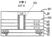
However, embodiments having a physical connection between the antenna module and the IC antenna may omit including a plug. As shown in fig. 7, a card formed in accordance with this aspect of the invention may include the following processing steps and structures:
step 1 — select the metal layer 30 intended to serve as the top layer of the card 10. The metal layer 30 has a top (front) surface 301 and a bottom (back) surface 302 and a thickness (D) that may range from less than 0.01 inches to greater than 0.02 inches. The metal layer 30 may have the same features and properties as the metal layer 30 shown and discussed above. As shown in step 1 of fig. 7, adhesive layer 42 is used to attach ferrite layer 44 to rear surface 302 of layer 30. The adhesive layer 46 is used to attach a plastic (e.g., PVC) layer 48 including the booster antenna 47 and/or having the booster antenna 47 mounted thereon to the ferrite layer. Layers 42, 44, 46, and 48 and enhanced antenna 47 are formed in a similar manner as the corresponding numbered components shown in fig. 2, and layers 42, 44, 46, and 48 and enhanced antenna 47 serve the same or similar functions. The assembly including layers 30, 42, 44, 46, and 48 is then laminated to form card assembly 750. Layer 52, including the signature panel and magnetic strip, may be attached to layer 48 before or after lamination. The layers 42, 44, 46, 48 (and possibly 52) may be formed into the subassembly 40 and attached to the bottom side 302 of the metal layer 30.
Step 2-hole 720 is formed through metal layer 30 and layers 42, 44, 46 until layer 48. Although shown as stopping at layer 48, in some embodiments, the holes may also cut through layer 48 (as is also true for other embodiments described and depicted herein). The lateral dimensions of the holes are nominally equal to, but slightly larger than, the lateral dimensions of the IC module (e.g., L1 and W1). The holes 720 may be formed in any known manner (e.g., milling, drilling, and/or any other suitable manner). The holes 720 may be regular or irregular solid cubes or cylinders that may be square, rectangular or circular or irregular in plan projection in the horizontal plane. The holes may also have a stepped configuration (T-shaped in cross-section) with a relatively wide portion facing the top surface of the card and a relatively narrow portion facing the bottom surface of the card, so that the chip, when inserted, rests on a metal shelf in the card body formed at the transition from the relatively narrow portion to the relatively wide portion. In the embodiment shown in fig. 7, the transverse dimensions of the bore 420 [ nominally length (L1) and width (W1) ] are only slightly larger than the transverse dimensions of the IC module [ also nominally length L1 and width W1] as discussed herein, wherein the difference between the bore dimensions and the module dimensions conforms to commercially acceptable tolerances.
Step 3-as shown in step 3 of fig. 7, a physical connection 700 is provided between the antenna module and the IC module. The physical connection may take any form as discussed with respect to the embodiment depicted in step 7 of fig. 2, except that because the hole 720 is not lined with a non-conductive plug, the physical connection may be insulated to avoid shorting to the hole walls. In one embodiment, as shown in step 2ALT a of fig. 7, a liner 760 may be placed on the sides of the hole prior to making the wired connection, for example, using a coating or annular plug inserted into the hole. The spacer 720 may have a length sufficient to cover the entire hole below the insertion depth of the IC module into the enhanced antenna, or it may cover only the metal portion of the hole. In another embodiment, at least a portion of the physical connection 700b disposed within a portion of the hole in the metal body may be an insulated wire (e.g., a conductive wire coated with a non-conductive coating). In another embodiment depicted in step 3 of fig. 7, the enhanced antenna layer 48 has a connection point 702a for connecting to an antenna via a connection segment 700a, and the IC module has a corresponding connection point 704 a. As depicted in fig. 8, modular connector 710 has mating connection points 702b and 704b for engaging with corresponding connection points in the antenna layer and IC chip, respectively, wherein conductive connection segments 700b connect connection points 702b and 704b within the connector. The lateral dimensions of the connector 710 are also nominally L1 and W1, within substantially the same commercial tolerances as those of the IC module, to allow snug insertion into the aperture 720. The connector may also have inserts of dimensions L3 and W3 that are smaller than L1 and W1, respectively, resulting in the formation of a ledge 738 that will provide support for the IC module and hold the IC module at its designed height D1 below top card surface 301. Also, in the embodiment depicted in step 2ALT a of fig. 7, liner 760 may be sized to provide an equivalent flange. The IC module 7 may be inserted snugly and attached (glued) to the top inner wall of the insert within the connector 710 and the flange 738. It should be understood that although depicted in connection with this embodiment, similar connector structures may be used with any of the other embodiments described herein to make physical connections, wherein the perimeter and side area of the connector match the corresponding perimeter and side area of the aperture into which it is inserted. In the embodiment depicted in step 3 of fig. 7, the body of the connector preferably comprises a non-conductive material in order to avoid any electrical connection between the traces 700b and/or between the traces and the walls of the hole 720 in the metal portion of the card.
As shown in step 3 of fig. 7, an IC module 7 including a chip 7a and a chip antenna 7b and a set of contacts 7c is positioned within the hole 436. The physical connections 700a, 700b extend between the booster antenna 47 and the chip antenna 7 b.
Although discussed in various places with respect to dimensions L1, W1 relative to dimension L2, W2 relative to dimension L3, W3, as noted herein, the present invention is not limited to rectangular embodiments, as noted above. Thus, when discussing the aspect that one element has a larger dimension than another element, it should be understood that references to structures having a relatively larger dimension, in non-rectangular embodiments, refer to structures having a relatively larger area, having a relatively larger perimeter located relatively radially outward of the comparative structure, as is true of the rectangular embodiments referred to in the examples.
Although the invention is illustrated and described herein with reference to specific embodiments, the invention is not intended to be limited to the details shown. Rather, various modifications may be made in the details within the scope and range of equivalents of the claims and without departing from the invention.
Claims (32)
1. A card having a card length, a card width, and a card thickness, the card comprising:
a metal layer having a top surface and a bottom surface extending parallel to each other;
an opening in the metal layer that (a) extends from the top surface to the bottom surface, or (b) is defined by a first area cut-out area in the top surface of the metal layer and a second cut-out area that extends from the bottom surface of the metal layer and extends vertically and substantially symmetrically about the first cut-out area below the first cut-out area;
an Integrated Circuit (IC) module disposed within the opening or the first cut-out region, the IC module having a depth D1, a first area, and a first perimeter, the IC module having contacts positioned along the top surface of the metal layer and configured to communicate using RF transmission to enable contactless operation;
a plug disposed within the opening or the second cutout region, the plug comprising a non-RF resistive material, the plug having a second area and a second perimeter equal to or greater than the first area and the first perimeter, respectively;
a ferrite layer disposed below the metal layer;
a vertical hole in the plug and extending through the ferrite layer, the vertical hole having a third area and a third perimeter that are smaller than the first area and the first perimeter, respectively; and
an enhanced antenna attached to the ferrite layer for enhancing RF transmission with the IC module.
2. The card of claim 1, wherein said first cut-out region has dimensions nominally equal to but slightly larger than D1, said first area and said first perimeter to facilitate snug fitting of said IC module disposed within said first cut-out region, said second cut-out region having a second area and a second perimeter larger than said first area and said first perimeter, respectively, said second cut-out region extending vertically up to a distance D1 from said top surface, wherein said plug is disposed within said second cut-out region.
3. A card according to claim 1, wherein the metal layer has a thickness D greater than D1, and the opening in the metal layer extends for the total thickness of the metal layer, the IC module mounted on the plug being located in the opening, the IC module and the plug extending between the top and bottom surfaces of the metal layer.
4. A card according to claim 3, wherein the second area and the second perimeter of the opening in the metal layer are larger than the first area and the first perimeter, respectively, and the plug is attached to the metal layer and fills the opening within the metal layer, and wherein the plug has a first cutout region having an area and a perimeter nominally equal to but slightly larger than the first area and the first perimeter, respectively, extending a depth nominally equal to but slightly larger than D1 below the top surface for receiving the IC module in a snug fit, and a second region below the first region extending up to a bottom surface of the metal layer.
5. The card of claim 4, further comprising a masking layer disposed over the top metal surface and any exposed portions of the plugs.
6. The card of claim 1, wherein the augmented antenna is configured to inductively couple to the IC module.
7. The card of claim 1, wherein the enhanced antenna is physically connected to the IC module.
8. A method of manufacturing a card according to claim 1, the method comprising the steps of:
selecting the metal layer;
cutting the second cut-out region in the metal layer starting from the bottom surface of the metal layer;
securely attaching the plug within the second cut-out region, the plug designed to fit within and fill the second cut-out region;
cutting the first cut-out region in the top surface of the metal layer covering the second cut-out region, the first cut-out region being symmetrically arranged with respect to the second cut-out region;
inserting and securely attaching the IC module within the first cut-out region, wherein contacts of the IC module are positioned along the same horizontal plane as a top surface of the metal layer;
attaching the ferrite layer to a bottom surface of the metal layer;
attaching the enhanced antenna layer to the ferrite layer;
forming the vertical hole in the plug and the ferrite layer.
9. The method of claim 8, further comprising laminating the metal layer, the ferrite layer, and the enhanced antenna layer.
10. The method of claim 9, further comprising physically connecting the augmented antenna to the IC module.
11. A method for manufacturing a card according to claim 3, the method comprising the steps of:
selecting the metal layer;
forming the opening;
securely attaching the plug within the opening; and
inserting the IC module into the plug first cut-out region and securely attaching the IC module within the plug first cut-out region;
attaching the ferrite layer to a bottom surface of the metal layer;
attaching the enhanced antenna layer to the ferrite layer; and
forming the vertical hole in the plug and the ferrite layer.
12. The method of claim 11, further comprising forming a masking layer formed over a top metal surface and any exposed portions of the plugs.
13. The method of claim 11, further comprising laminating the metal layer, the ferrite layer, and the enhanced antenna layer.
14. A metal smart card with dual interface capability, comprising:
a metal layer having a thickness D, the metal layer having a top surface and a bottom surface extending parallel to each other, the top surface defining a horizontal plane;
an Integrated Circuit (IC) module having a top region with contacts configured for physical contact with a card reader, the IC module further configured for contactless Radio Frequency (RF) communication with the card reader, the IC module having a first perimeter, a first area, and a thickness D1, wherein D1 is less than D;
a plug of non-RF resistive material having a second perimeter and a second area equal to or greater than the first perimeter and the first area, respectively;
an opening in the metal layer extending for the total thickness of the metal layer, the IC module being mounted on the plug disposed in the opening, the IC module and the plug extending in a vertical direction between a top surface and a bottom surface of the metal layer, wherein contacts of the IC module are located along the same horizontal plane as the top surface of the metal layer, the opening in the metal layer having a first region located at the top surface and just below the top surface for receiving the IC module and a second region below the first region extending up to the bottom surface of the metal layer, the opening in the first region having lateral dimensions nominally equal to but slightly larger than the first area and the first perimeter for a depth nominally equal to but slightly larger than D1, for a depth of the remaining thickness of the card under the first region, the second region having a second area and a second perimeter, wherein the IC module fits in and fills the opening in the first region and the plug fits in and fills the opening in the second region, wherein the second area and the second perimeter are greater than the first area and the first perimeter, respectively; and
a masking layer disposed over the top metal surface and any exposed portions of the plugs;
a ferrite layer disposed below the metal layer;
a vertical hole formed in the plug and through the ferrite layer, the vertical hole having a third area and a third perimeter that are smaller than the first area and the first perimeter, respectively; and
an enhanced antenna attached to the ferrite layer for enhancing RF transmission with the IC module.
15. The card of claim 14, wherein the augmented antenna is configured to inductively couple to the IC module.
16. The card of claim 14, wherein the enhanced antenna is physically connected to the IC module.
17. A card, comprising:
a metal layer having a top surface and a bottom surface extending parallel to each other.
A first region cut in the top surface of the metal layer, the first region having a first depth, a first perimeter, and a first area;
an Integrated Circuit (IC) module snugly secured within the first cut-out region, the IC module having contacts positioned along a top surface of the metal layer and configured to communicate using RF transmissions to enable contactless operation;
a second cut-out region extending from the bottom surface of the metal layer up to the first depth from the top surface, the second cut-out region extending vertically below the first cut-out region and substantially symmetrically about the first cut-out region, the second cut-out region having a second area and a second perimeter that are greater than the first area and the second perimeter; and
a plug formed of a non-RF resistive material snugly secured within the second cutout area;
a ferrite layer disposed below the metal layer;
a vertical hole formed in the plug and through the ferrite layer, the vertical hole having a third area and a third perimeter that are smaller than the first area and the first perimeter, respectively; and
an enhanced antenna attached to the ferrite layer for enhancing RF transmission with the IC module.
18. The card of claim 17, wherein the augmented antenna is configured to inductively couple to the IC module.
19. The card of claim 17, wherein the enhanced antenna is physically connected to the IC module.
20. A card, the card comprising:
a metal layer having a top surface and a bottom surface extending parallel to each other, and a thickness extending between the top surface and the bottom surface;
a ferrite layer disposed below the metal layer;
an enhanced antenna disposed below the ferrite layer for enhancing RF transmission with the IC module;
openings in the metal layer and the ferrite layer that extend to the enhanced antenna layer;
an Integrated Circuit (IC) module having a first area, a first perimeter, and a first depth that is less than a thickness of the metal layer, the IC module being disposed within the opening and having contacts positioned along a top surface of the metal layer and configured to communicate using RF transmission to enable contactless operation; and
a physical electrical connection between the enhanced antenna and the IC module that extends through the opening.
21. The card of claim 20, further comprising a non-conductive liner in the opening in the metal layer.
22. The card of claim 20, wherein said non-conductive liner comprises a plug of non-conductive material, wherein said plug has a second area and a second perimeter that are greater than said first area and said first perimeter, respectively.
23. A card according to claim 22, wherein the plug has the second area and the second perimeter, a depth extending for the total thickness of the metal layer, and further comprising a cut-out region in the plug nominally equal to but slightly greater than the first area, the first perimeter and the first depth for receiving the IC module in the cut-out region, the plug further having a through hole extending from the cut-out region for the remaining depth of the plug and connected to an opening in the ferrite layer, the through hole in the plug and the opening in the ferrite layer having a third area and a third perimeter smaller than the first area and the first perimeter, respectively.
24. The card of claim 22, wherein the opening is a stepped opening having a first area nominally equal to but slightly larger than the first area, the first perimeter, and the first depth to snugly fit the IC module in the opening and a second area having the second area and the second perimeter, a depth extending from a bottom surface of the metal layer by a distance less than a total thickness of the metal layer, wherein the plug is disposed only in the second area, the plug having a via connected to the opening in the ferrite layer, the via in the plug and the opening in the ferrite layer having a third area and a third perimeter smaller than the first area and the first perimeter, respectively.
25. The card of claim 20, wherein the opening has an area and a perimeter nominally equal to but slightly larger than the first and second areas, and the physical electrical connection between the enhanced antenna and the IC module comprises a connection module disposed between the enhanced antenna and the IC module.
26. The card of claim 25, wherein the enhanced antenna has a first connection node and a second connection node, and the IC module has a third connection node and a fourth connection node, and the connection module has a mating first connection node and a mating second connection node on a first surface thereof and a mating third connection node and a mating fourth connection node on a second surface thereof, a first conductive trace connecting the first node and the third node, and a second conductive trace connecting the second node and the fourth node.
27. A method of manufacturing a card according to claim 20, the method comprising the steps of:
selecting the metal layer;
attaching the ferrite layer under the metal layer;
attaching the enhanced antenna layer below the ferrite layer;
forming the opening in the metal layer extending through the ferrite layer to the booster antenna; and
inserting and securely attaching the IC module in the opening, wherein contacts of the IC module are located along the same horizontal plane as a top surface of the metal layer and the IC module is physically connected to the enhanced antenna layer.
28. The method of claim 27, wherein the method comprises: first forming the opening in the metal layer and disposing a plug in at least a portion of the opening in the metal layer, at least a portion of the plug having a second area and a second perimeter that are greater than the first area and the first perimeter, respectively; and creating a via in the plug and creating the opening in the ferrite layer, the via in the plug and the opening in the ferrite layer having a third area and a third perimeter that are less than the first area and the first perimeter, respectively.
29. The method of claim 28, wherein the method comprises: first forming a bottom portion of the opening in the metal layer that is less than a total thickness of the metal layer, the bottom portion having the second area and the second perimeter; and disposing the plug in the bottom portion of the metal layer; then creating a via in the plug and creating the opening in the ferrite layer, the via in the plug and the opening in the ferrite layer having a third area and a third perimeter that are smaller than the first area and the first perimeter, respectively.
30. The method of claim 27, wherein the method comprises: first laminating the metal layer, the ferrite layer under the metal layer, and the enhanced antenna layer together; the opening extending through the ferrite layer to the booster antenna is then formed in the metal layer, wherein the opening has an area and a perimeter nominally equal to but slightly larger than the first area and the first perimeter, respectively.
31. The method of claim 30, further comprising: disposing a gasket in the opening prior to inserting and securely attaching the IC module in the opening and connecting the IC module to the enhanced antenna layer.
32. The method of claim 30 wherein the enhanced antenna layer has a plurality of connection nodes and the IC module has a plurality of connection nodes, the method further comprising disposing a connector in the opening prior to inserting the IC module into the opening, the connector having a junction node for connecting to an enhanced antenna connection node and an IC module connection node.
Applications Claiming Priority (3)
| Application Number | Priority Date | Filing Date | Title |
|---|---|---|---|
| US15/976,612 | 2018-05-10 | ||
| US15/976,612 US10318859B2 (en) | 2015-07-08 | 2018-05-10 | Dual interface metal smart card with booster antenna |
| PCT/US2019/012685 WO2019136436A1 (en) | 2018-01-08 | 2019-01-08 | Dual interface metal smart card with booster antenna |
Publications (1)
| Publication Number | Publication Date |
|---|---|
| CN112384932A true CN112384932A (en) | 2021-02-19 |
Family
ID=67144003
Family Applications (1)
| Application Number | Title | Priority Date | Filing Date |
|---|---|---|---|
| CN201980045848.7A Pending CN112384932A (en) | 2018-05-10 | 2019-01-08 | Dual-interface metal smart card with enhanced antenna |
Country Status (13)
| Country | Link |
|---|---|
| EP (2) | EP3791323A4 (en) |
| JP (2) | JP7007500B2 (en) |
| KR (2) | KR20220027286A (en) |
| CN (1) | CN112384932A (en) |
| AU (2) | AU2019205433B2 (en) |
| BR (1) | BR112020022946A2 (en) |
| CA (1) | CA3099670C (en) |
| CO (1) | CO2020014125A2 (en) |
| MX (2) | MX2021013094A (en) |
| NZ (1) | NZ769702A (en) |
| SG (1) | SG11202011081WA (en) |
| WO (1) | WO2019136436A1 (en) |
| ZA (2) | ZA202007106B (en) |
Families Citing this family (4)
| Publication number | Priority date | Publication date | Assignee | Title |
|---|---|---|---|---|
| US11551050B2 (en) | 2020-11-12 | 2023-01-10 | Advanide Holdings Pte. Ltd. | Card inlay for direct connection or inductive coupling technology |
| DE102021000384A1 (en) * | 2021-01-26 | 2022-07-28 | Giesecke+Devrient Mobile Security Gmbh | Card body for a chip card and chip card |
| KR20230171088A (en) * | 2022-06-10 | 2023-12-20 | 코나엠 주식회사 | A wireless IC metal card with clad metal structure and a manufacturing method thereof |
| KR20230170503A (en) * | 2022-06-10 | 2023-12-19 | 코나엠 주식회사 | A metal card including insert coil and manufacturing it |
Citations (5)
| Publication number | Priority date | Publication date | Assignee | Title |
|---|---|---|---|---|
| CN103907125A (en) * | 2011-08-08 | 2014-07-02 | 菲尼克斯阿美特克有限公司 | Improving coupling in and to rfid smart cards |
| US9390366B1 (en) * | 2015-07-08 | 2016-07-12 | Composecure, Llc | Metal smart card with dual interface capability |
| CN105793872A (en) * | 2013-11-18 | 2016-07-20 | 安全创造有限责任公司 | Card with a metal layer and an antenna |
| CN106575373A (en) * | 2015-07-08 | 2017-04-19 | 安全创造有限责任公司 | Metal smart card with dual interface capability |
| CN206711130U (en) * | 2017-05-15 | 2017-12-05 | 金邦达有限公司 | Can two-sided radio-frequency communication metal chip card |
Family Cites Families (12)
| Publication number | Priority date | Publication date | Assignee | Title |
|---|---|---|---|---|
| US6016432A (en) * | 1993-03-04 | 2000-01-18 | Telefonaktiebolaget L/M Ericsson (Publ) | Electronic metering equipment system |
| US7762471B2 (en) * | 2006-09-07 | 2010-07-27 | Mastercard International, Inc. | Proximity payment card with cost-effective connection between user-actuatable input switch and RFID IC |
| JP2009157666A (en) | 2007-12-27 | 2009-07-16 | Dainippon Printing Co Ltd | Contact/non-contact sharing type ic card, non-contact type ic card and method for manufacturing the same |
| US8366009B2 (en) * | 2010-08-12 | 2013-02-05 | Féinics Amatech Teoranta | Coupling in and to RFID smart cards |
| JP5337834B2 (en) * | 2011-03-31 | 2013-11-06 | 富士フイルム株式会社 | RFID tag and RFID communication system |
| US9798968B2 (en) * | 2013-01-18 | 2017-10-24 | Féinics Amatech Teoranta | Smartcard with coupling frame and method of increasing activation distance of a transponder chip module |
| CA2860909C (en) * | 2012-01-23 | 2021-11-16 | David Finn | Offsetting shielding and enhancing coupling in metallized smart cards |
| KR101602381B1 (en) * | 2012-06-26 | 2016-03-21 | 도요세이칸 그룹 홀딩스 가부시키가이샤 | Rf tag |
| WO2014113765A1 (en) | 2013-01-21 | 2014-07-24 | Composecure, Llc | Metal card with radio frequency (rf) transmission capability |
| DE102013018518A1 (en) * | 2013-11-04 | 2015-05-07 | Giesecke & Devrient Gmbh | IC module for different connection techniques |
| BR112016027213B1 (en) * | 2014-05-22 | 2022-11-01 | Composecure, Llc | ID AND TRANSACTION CARDS THAT HAVE SELECTED TEXTURE AND COLOR AND METHOD FOR PRODUCING THE SAME |
| WO2016106251A2 (en) * | 2014-12-23 | 2016-06-30 | Composecure, Llc | Smart metal card with radio frequency (rf) transmission capability |
-
2019
- 2019-01-08 SG SG11202011081WA patent/SG11202011081WA/en unknown
- 2019-01-08 MX MX2021013094A patent/MX2021013094A/en unknown
- 2019-01-08 BR BR112020022946-6A patent/BR112020022946A2/en unknown
- 2019-01-08 MX MX2020011971A patent/MX2020011971A/en unknown
- 2019-01-08 CA CA3099670A patent/CA3099670C/en active Active
- 2019-01-08 NZ NZ769702A patent/NZ769702A/en active IP Right Revival
- 2019-01-08 KR KR1020227005922A patent/KR20220027286A/en active Search and Examination
- 2019-01-08 EP EP19736107.4A patent/EP3791323A4/en active Pending
- 2019-01-08 KR KR1020207032191A patent/KR102367944B1/en active IP Right Grant
- 2019-01-08 AU AU2019205433A patent/AU2019205433B2/en active Active
- 2019-01-08 WO PCT/US2019/012685 patent/WO2019136436A1/en active Application Filing
- 2019-01-08 JP JP2020563599A patent/JP7007500B2/en active Active
- 2019-01-08 CN CN201980045848.7A patent/CN112384932A/en active Pending
- 2019-01-08 EP EP22187110.6A patent/EP4145347A1/en active Pending
-
2020
- 2020-11-11 CO CONC2020/0014125A patent/CO2020014125A2/en unknown
- 2020-11-13 ZA ZA2020/07106A patent/ZA202007106B/en unknown
-
2021
- 2021-04-19 AU AU2021202354A patent/AU2021202354B2/en active Active
- 2021-11-08 ZA ZA2021/08744A patent/ZA202108744B/en unknown
-
2022
- 2022-01-06 JP JP2022001057A patent/JP7234422B2/en active Active
Patent Citations (5)
| Publication number | Priority date | Publication date | Assignee | Title |
|---|---|---|---|---|
| CN103907125A (en) * | 2011-08-08 | 2014-07-02 | 菲尼克斯阿美特克有限公司 | Improving coupling in and to rfid smart cards |
| CN105793872A (en) * | 2013-11-18 | 2016-07-20 | 安全创造有限责任公司 | Card with a metal layer and an antenna |
| US9390366B1 (en) * | 2015-07-08 | 2016-07-12 | Composecure, Llc | Metal smart card with dual interface capability |
| CN106575373A (en) * | 2015-07-08 | 2017-04-19 | 安全创造有限责任公司 | Metal smart card with dual interface capability |
| CN206711130U (en) * | 2017-05-15 | 2017-12-05 | 金邦达有限公司 | Can two-sided radio-frequency communication metal chip card |
Also Published As
| Publication number | Publication date |
|---|---|
| AU2021202354A1 (en) | 2021-05-13 |
| AU2021202354B2 (en) | 2022-08-04 |
| JP7007500B2 (en) | 2022-01-24 |
| EP3791323A1 (en) | 2021-03-17 |
| MX2021013094A (en) | 2023-04-14 |
| EP3791323A4 (en) | 2022-08-10 |
| CO2020014125A2 (en) | 2020-11-30 |
| BR112020022946A2 (en) | 2021-09-08 |
| CA3099670A1 (en) | 2019-07-11 |
| NZ769702A (en) | 2022-12-23 |
| CA3099670C (en) | 2022-08-23 |
| JP2021515346A (en) | 2021-06-17 |
| KR20220027286A (en) | 2022-03-07 |
| ZA202007106B (en) | 2022-03-30 |
| EP4145347A1 (en) | 2023-03-08 |
| ZA202108744B (en) | 2023-07-26 |
| MX2020011971A (en) | 2021-10-26 |
| AU2019205433A1 (en) | 2020-12-03 |
| KR20210018995A (en) | 2021-02-19 |
| AU2019205433B2 (en) | 2021-04-08 |
| JP2022048179A (en) | 2022-03-25 |
| WO2019136436A1 (en) | 2019-07-11 |
| JP7234422B2 (en) | 2023-03-07 |
| SG11202011081WA (en) | 2020-12-30 |
| KR102367944B1 (en) | 2022-02-24 |
Similar Documents
| Publication | Publication Date | Title |
|---|---|---|
| US11301744B2 (en) | Metal smart card with dual interface capability | |
| CN106575373B (en) | Metal smart card with dual interface capability | |
| US9390366B1 (en) | Metal smart card with dual interface capability | |
| AU2021202354B2 (en) | Dual interface metal smart card with booster antenna | |
| US10275703B2 (en) | Smart metal card with radio frequency (RF) transmission capability | |
| US20240119249A1 (en) | Metal dual interface card | |
| US20230237305A1 (en) | Method for manufacturing a metal chip card with mini relay antenna |
Legal Events
| Date | Code | Title | Description |
|---|---|---|---|
| PB01 | Publication | ||
| PB01 | Publication | ||
| SE01 | Entry into force of request for substantive examination | ||
| SE01 | Entry into force of request for substantive examination |