Purpose of the present invention is for avoiding the above-mentioned fact and improved data vehicle is provided and is used for the improved circuit of data vehicle with plain mode, and they have the support and the minimum expense of minimum device.
According to the present invention, in order to achieve the above object, in first section in the data vehicle of defined type, data link is constituted the actuating logic OR function, and according to this structure, thereby make data link be suitable for they first data input device and second data input device on the data that receive simultaneously be sent to simultaneously on their data output device and to data processing equipment.This structure of data vehicle has data link can be with the very big advantage of very simple therefore low-cost circuit realization.In addition, this structure further has the very big advantage that does not need and can save the independent controlling features that is used for data link, and in order to realize simple as far as possible circuit, this also is very favorable.Had according to structure of the present invention, in fact very rare situation-at this moment activate simultaneously contact connection mode and contactless pattern may appear, this is that in fact few appearance the-i.e. appearance reaches the data that receive by the contactless interface arrangement by contact connecting interface device, and they constitute out of use data mixing thing.Yet in fact there is not practical problems in this, because if this out of use data mixing thing occurs, data processing equipment can detect the existence of this out of use data mixing thing and can forbid further handling this data mixing thing.
In according to data vehicle of the present invention, data link can constitute with two diodes basically, and these two diodes for example are connected their positive pole on the data output device of data link and their negative pole is connected to each other and is connected on the data input device of data link.Yet, in according to data vehicle of the present invention,, turned out to be advantageous particularly if data link is to constitute with OR-gate.Owing in the situation of OR-gate, on the data output device of data link, always can obtain the result of full level, compare the advantage that this OR-gate has the no-voltage loss occurrence with diode.
In according to data vehicle of the present invention, if data processing equipment comprises the data output device that is used for exporting the data that will export in contact connection mode and contactless pattern in addition, contact connecting interface device comprises the contact that is used for receiving the data that will export at the contact connection mode and connects data input device, the contactless interface arrangement comprises the contactless data input device that is used for receiving the data that will export in the contactless pattern, the contactless data input device that the contact of the data output device of data processing equipment and contact connecting interface device connects data input device and contactless interface arrangement is to be electrically connected mutually, then further confirms it is favourable.In view of simple especially circuit design, this is very favorable.Should point out that defined measure also can advantageously be applied in according to using on the data vehicle of the present invention of OR-gate as data link in this paragraph.
For according to data vehicle of the present invention, if be provided with device in addition, it causes that when the contact connection mode is inactive the contact of contact connecting interface device is connected data output device and is set at state corresponding to logical zero, and be provided with another device, it causes when inactive contactless data output device with the contactless interface arrangement to be set at state corresponding to logical zero similarly under the contactless pattern, has then also confirmed it is favourable.In view of the on off state of unambiguity definition and the failure-free operation that draws thus, this is favourable.
On according to data vehicle of the present invention, if be provided with pick-up unit in addition, it can detect activated contact connection mode and contactless pattern both, and it is when detecting contact connection mode and contactless pattern both and activated, can cause the forbidden data treating apparatus to be handled and act on data on the described data processing equipment, then further turn out to be favourable by their data input device.In view of the reliable and trouble-free performance according to data vehicle of the present invention, this is favourable.
In according to data vehicle of the present invention, if pick-up unit constitutes with clock signal detection device in addition, it can detect when the contact connection mode activates, and the contact that occurs connects the existence of clock signal and the existence of the contactless clock signal that occurs when the contactless mode activation, has then turned out to be particularly advantageous.In the practice, confirmed this embodiment especially effectively with favourable, to have activated the contact connection mode with the detection of unambiguity ground in according to data vehicle of the present invention still be the contactless pattern because clock signal allows to be perfectly clear.
According to the present invention, in order to achieve the above object, the circuit of defined type is characterised in that this data link constitutes the actuating logic OR function in second section, and according to this structure, thus data link be suitable for they first data input device and second data input device on the data that receive simultaneously be sent to their data output device simultaneously and to data processing equipment.In this way, for according to the obtainable advantage of circuit of the present invention corresponding to described advantage before this according to data vehicle of the present invention.
According to the modification of circuit of the present invention, the advantage that their produce is corresponding to the advantage described above according to the favourable modification of data vehicle of the present invention.
From the following embodiment that describes by way of example and illustrate with reference to present embodiment, above-mentioned aspect of the present invention and other aspect will be conspicuous.
Describe the present invention below with reference to two embodiment that also provide by way of example shown in the figure, but the invention is not restricted to this.
Fig. 1 illustrates according to the data vehicle 1 of the first embodiment of the present invention and is used for the diagrammatic representation of block scheme form of a part of the circuit 2 of data vehicle 1.In this example, data vehicle 1 is so-called composite card (combi-card).Circuit 2 adopts the integrated circuit form.
This data vehicle 1 and circuit 2 thereof can be worked in so-called contact connection mode and so-called contactless pattern.For this purpose, data vehicle 1 comprises contact connecting interface device 3 and contactless interface arrangement 4.
Contact connecting interface device 3 comprises the crosspoint array 5 that is made of 8 contacts 6,7,8,9,10,11,12 and 13 altogether, by these 8 contacts, data vehicle 1 can be cooperated with the Writing/Reading equipment that constitutes accordingly that is applicable to this purpose with the contact connected mode in its contact connection mode the time.Contact connecting interface device 3 also comprises schematically shown in Figure 1 the contact that is connected on the contact of crosspoint array 5 by circuit 15 and connects signal component 14.When enlivening, the contact connection mode might receive data by contact connecting interface device 3, these data can connect at contact to be handled in the signal component 14 also and can connect the contact connection data output device 16 that signal component 14 is transferred to contact connecting interface device 3 from contact, and the effect of this output unit is the data that output is received when the contact connection mode enlivens.In this example, contact connects data output device 16 and is made of the signal data output contact, might connect signal component 14 with contact by it the data that provide with series form are provided.Yet, as an alternative, contact can be connected signal component 14 and constitute with these parts and provide the mode of these data to handle the data that receive from crosspoint array 5 with parallel form, the contact of contact connecting interface device connects data output device and comprises a plurality of data output contacts in this case.
Contact connecting interface device 3 also comprises the contact connection data input device 17 that is used for receiving when the contact connection mode enlivens at data vehicle 1 data that provide.In this example, these contacts connect data input device 17 and also comprise the individual data input contact that can with serial mode data be sent to the contact connection signal component 14 of contact connecting interface device 3 by it.
Contactless interface arrangement 4 comprises transmission coil 18, can be by it with induction, it is contactless, mode is from being applicable to the Writing/Reading equipment receiving data that constitutes accordingly of this purpose, and can be that the contactless mode sends the data that data vehicle 1 provides to tranmission/reception apparatus with induction in the opposite direction by it.Contactless interface arrangement 4 also comprises the contactless signal component 19 that is connected on the transmission coil 18.The DSR that the data of utilizing contactless signal component 19 energy regenerative transmission coils 18 to receive also can will be transmitted transmission coil 18 is for transmission.Thereby might in the contactless pattern, receive data by contactless interface arrangement 4, and handling the contactless data output device 20 that transfers them to contactless interface arrangement 4 with regeneration after them with contactless signal component 19, the latter is used for the data that output is received when the contactless pattern is enlivened, in this example, contactless data output device 20 includes only a signal data output contact.Should point out that be similar to contact and connect data output device 16, the contactless data output device also can comprise a plurality of data output contacts when needed.
Contactless interface arrangement 4 also is included in the contactless data input device 21 that is used to receive the data that provide when the contactless pattern is enlivened.In this example, the contactless data input device 21 of contactless interface arrangement 4 also includes only individual data input contact.
Data vehicle 1 and circuit 2 thereof also comprise data processing equipment 22.Data that data processing equipment 22 is used to handle when the contact connection mode enlivens and the contactless pattern receives when enlivening and be used for handling when the contact connection mode enlivens and the contactless pattern will provide when enlivening, the i.e. data that will transmit.Data processing equipment 22 comprises the data input device 23 that is used for being received in the data that contact connection mode and contactless pattern received.In this example, data input device 23 includes only individual data input contact.Data processing equipment 22 also has the data output device 24 that is used for exporting the data that provide in contact connection mode and contactless pattern.Data output device 24 also includes only the individual data output contact in this example.
Data processing equipment 22 is connected on the memory storage 26 by bus 25.Memory storage 26 is made of so-called EEPROM.Yet also available as an alternative so-called RAM constitutes memory storage 26, yet RAM should accept supply voltage incessantly in this case.Memory storage 26 can be stored the data that reach data processing equipment 22 processing that data vehicle 1 receives.In addition, data processing equipment 22 can be read the data that are stored in the memory storage 26 by bus 25 from memory storage 26, so that when the contact connection mode enlivens, send read/write device to, and when enlivening, the contactless pattern sends tranmission/reception apparatus to by contactless interface arrangement 4 by contact connecting interface device 3.
Data vehicle 1 and circuit 2 thereof also comprise data link 27.Data link 27 comprises first data input device 28, second data input device 29 and data output device 30.The contact that first data input device 28 is connected contact connecting interface device 3 connects on the data output device 16.Second data input device 29 is connected on the contactless data output device 20 of contactless interface arrangement 4.Data output device 30 is connected on the data input device 23 of data processing equipment 22.Data link 27 can send the data that receive and act on the data on first data input device 28 and receive and act on second data input device 29 in the contact connection mode in the contactless pattern to data processing equipment 22 by data output device 30.The structure of data link 27 guarantees to forbid in data link 27 to transmit the data that receive or the data that transmission received to other data input device 29 or 28 from data input device 28.
In the data vehicle 1 shown in Fig. 1, data link 27 is advantageously to constitute according to the logical "or" function.Thereby this structure of data link 27 allows data link 27 to send the data that first data input device 28 and second data input device 29 of these data links receives simultaneously to data output device 30 simultaneously also to data processing equipment 22.
Can be thereby data vehicle 1 and circuit 2 thereof have data link 27 as very big advantage very simple and circuit realization cheaply.This structure also has the very big advantage of the independent control device that does not need to be used for data link 27, and this is also highly beneficial for simple circuit design.
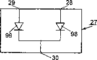
Fig. 2 only illustrates according to the data link 27 of the data vehicle of the second embodiment of the present invention and the circuit of this data vehicle.Apparent from Fig. 2, data link 27 comprises first diode 98 and second diode 99.First diode 98 is configured between first data input device 28 and the data output device 30, and its positive electrical is connected first data input device 28 with first diode 98 and negative pole is connected on the data output device 30.Second diode 99 is configured between second data input device 29 and the data output device 30, and second diode 99 is connected its positive electrical on second data input device 29 and negative pole is connected on the data output device 30.
Should point out in according to the data vehicle of the second embodiment of the present invention and circuit according to the second embodiment of the present invention, in two diodes 98 and 99 back, the stray capacitance in the present circuit block of should taking steps to allow to discharge-it in two diodes 98 and 99 back and finally by the data processing equipment 22 input circuit parts of back constitute-it can charge with 99 by two diodes 98.For these stray capacitances of discharging, the data output device 30 that can cross over data link 27 is provided with the independent grounding resistor that is also referred to as pull-down-resistor, and this resistor can have for example resistance value in 10k Ω and 100k Ω scope.
Fig. 3 illustrates according to the another data vehicle 1 of the third embodiment of the present invention and the circuit 2 of this data vehicle 1.About the data vehicle 1 of Fig. 3, except explanation, following content be proposed with reference to the data vehicle 1 of figure 1.
As can be seen from Fig. 3, the contact 9 of crosspoint array 5 is used to apply power supply potential VCC at data vehicle 1.Contact 13 is used to apply earth potential.Contact 7 is used to apply contact and connects clock signal KB-CLK, and it has the frequency of about 5.0MHz in this example.The contact 11 of crosspoint array 5 constitutes the data input/output interface (I/O) that can transmit data by it with series form.
Contact in the data vehicle 1 of Fig. 3 connects signal component 14 and comprises the circuit for signal conditioning 31 and the first clock signal treatment circuit 32.
One side of circuit for signal conditioning 31 is connected by bidirectional line 33 on the contact 11 of crosspoint array 5, and its opposite side is connected on the contact connection data output device 16 and is connected contact by another one-way line 35 by one-way line 34 and connects on the data input device 17.Utilize circuit for signal conditioning 11 can handle data-signal that the contact 11 by crosspoint array 5 receives and act on data-signal above it by bidirectional line 33, connect on the data output device 16 so that treated data-signal is acted on contact, and the data-signal of energy regulating action on contact connection data input device 17 is so that act on it on contact 11 of crosspoint array by bidirectional line 33.
The contact that the first clock signal treatment circuit 32 is used to handle on the input end 36 that acts on the first clock signal treatment circuit 32 connects clock signal KB-CLK.Utilize clock signal treatment circuit 32 palingenesiss contact thereon to connect clock signal KB-CLK and its first clock signal clk 1 as regeneration is acted on first output terminal 37 of the first clock signal treatment circuit 32.First clock signal clk 1 also has the frequency of 5.0MHz.The contact of the first clock signal treatment circuit 32 above acting on it connects clock signal KB-CLK further derives second clock signal CLK2, and this second clock signal has the frequency of 9.6KHz and offers second output terminal 38 of the first clock signal treatment circuit 32.
For the data vehicle 1 of Fig. 3, should point out that this contactless signal component 19 comprises simulating signal parts 39 and decoder stage 40, code level 41 and two clock signal treatment circuits 42.
In mode known per se, simulating signal parts 39 comprise power supply potential and generate level 43, clock regenerating signal level 44, demodulator stage 45 and modulator stage 46.Described level Four 43,44,45 and 46 respectively is connected on the transmission coil 18 in a not shown manner.
Utilize power supply potential to generate level 43, can from the signal that receives with transmission coil 18, derive power supply potential VDD.All circuit stages of utilizing power supply potential VDD to power to give the circuit 2 of needed data vehicle 1 in the contactless pattern, for example to shown in decoder stage 40, can be by power supply potential input end 47 effect power supply potential VDD.
Should point out, can act on power supply potential VCC on the data vehicle 1 be used for powering all circuit blocks by the contact 9 of crosspoint array 5 at the required data vehicle 1 of contact connection mode.As a result, power supply potential VCC can be acted on and carry out on all required circuit blocks of contact connection mode, as with shown in the by way of example, for circuit for signal conditioning 31, power supply potential VCC can be by 48 effects of power supply potential input end thereon.
Utilize clock regenerating signal level 44, can derive the contactless clock signal KL-CLK that is included in wherein from the signal that receives with transmission coil 18, this clock signal has the frequency of 13.56MHz in this example.In this example, clock regenerating signal level 44 derives the 3rd clock signal clk 3 from the contactless clock signal KL-CLK that receives, the 3rd clock signal can be acted on the input end 49 of clock signal treatment circuit 42.Second clock signal processing circuit 42 sends the frequency that the 3 essentially no any changes of the 3rd clock signal clk reach with 3.39MHz to first output terminal 50.Derive two further clock signals the 3rd clock signal clk 3 of second clock signal processing circuit 42 above acting on it, promptly have the 4th clock signal clk 4 and the 5th clock signal clk 5 of the frequency of 800KHz with 106KHz frequency.Second clock signal processing circuit 42 offers the 4th clock signal clk 4 second output terminal 51 and the 5th clock signal clk 5 is offered the 3rd output terminal 52.
The demodulator stage 45 of simulating signal parts 39 is used to separate the data-signal that calls transmission coil 18 receptions.Can the process demodulated data signal that demodulator stage 45 is provided be acted on the input end 54 of decoder stage 40 by one-way line 53.In addition, the 5th clock signal clk 5 can be acted on another input end 55 of decoder stage 40.Utilize suitable decode procedure, decoder stage 40 can be with data-signal-it comprises such as the simple data layout of the data of given line codes such as Miller sign indicating number-be decoded into, i.e. the sequence of the position of a presentation logic zero or logic one.Can the data of decoding be acted on the contactless data output device 20 by the output terminal 56 of decoder stage 40.Should point out that for decoder stage 40 this one-level only just provides data detecting when significant coded data acts on the input end 54.
Contactless signal component 19 comprises the code level 41 that is similar to decoder stage 40, and it has the input end 27 that is connected on the contactless data input device 21, data can be acted on the code level 41 by this input end.In addition, can the 4th clock signal clk 4 be acted on the code level 41 by another input end 97.Data available code level 41 codings of exporting.Coded data is to be sent on the output terminal 58 and to act on by one-way line 59 on the modulator stage 46 of simulating signal parts 39 from code level 41.Subsequently, modulator stage 46 is carried out the modulated process that allows to be sent to tranmission/reception apparatus.Modulated process can be such as so-called load-modulate.
Data vehicle 1 and the circuit 2 thereof of Fig. 3 comprise clock signal detection device 60, detect with its that the contact occur in the contact connection mode connects the existence of clock signal KB-CLK and the existence of the contactless clock signal KL-CLK that occurs in the contactless pattern.For this purpose, by circuit 61 contact being connected clock signal KB-CLK acts on the first input end 62 of clock signal detection device 60 from the contact 7 of crosspoint array 5.In addition, will act on second input end 64 of clock signal detection device 60 corresponding to the 3rd clock signal clk 3 of contactless clock signal KL-CLK by another circuit 63.
Clock signal detection device 60 makes it to detect whether clock signal KB-CLK or CLK3 occur on input end 62 or 64 separately, and detect whether simultaneously on two input ends 62 and 64, clock signal KB-CLK and CLK3 occur, promptly activated contact connection mode and contactless pattern both because only in above-mentioned situation two clock signal KB-CLK and CLK3 just appear on two input ends 62 and 64 of clock signal detection device 60.Thereby clock signal detection device 60 constitutes and may detect the additional detection means that activates contact connection mode and contactless pattern with it.
When detecting contact on the input end 62 of clock signal supervisory instrument 60 at them and connect existing of clock signal KB-CLK, clock signal detection device 60 generates contact connection control information KBSI on first output terminal 65.When detecting the existing of the 3rd clock signal clk 3 on second input end 64 of clock signal supervisory instrument 60 at them, clock signal detection device generates contactless control information KLSI on their first output terminal 65.When detecting two clock signal KB-CLK and KB-CLK3 on two input ends 62 and 64 of clock signal supervisory instrument 60 at them, existing, clock signal detection device 60 also generates contact connection control information KBSI on their output terminal 65, this means that the contact connection mode has the so-called function of tonic chord in this case, and clock signal detection device 60 generates prohibition information BI on second output terminal 66.
The control input end 67 of switching clock signal equipment 68 is connected on first output terminal 65 of clock signal detection device 60.Switching clock signal equipment 68 has first clock signal input terminal 69, second clock signal input part 70 and clock signal output part 71.First clock signal input terminal 69 is connected on the output terminal 38 of the first clock signal treatment circuit 32, as its result, second clock signal CLK2 with 9.6KHz frequency can be acted on first clock signal input terminal 69, this frequency is corresponding to the data transmission rate in the contact connection mode.Second clock signal input part 70 is connected on the 3rd output terminal 52 of second clock signal processing circuit 42, as its result, the 5th clock signal clk 5 can be acted on the second clock signal input part 70, the 5th clock signal has the frequency of 106KHz, and it is corresponding to the data transmission rate in the contactless pattern.
When contact connection control information KBSI acted on the switching clock signal equipment 68, switching clock signal equipment 68 provided the connection from first clock signal input terminal 69 to clock signal output part 71.When contactless control information KLSI acted on the switching clock signal equipment 68, switching clock signal equipment 68 provided the connection from second clock signal input part 70 to clock signal output part 71.Thereby, on clock signal output terminal 71, always can obtain clock signal required in the instantaneous active mode.
For the circuit for signal conditioning 31 in the contact connection signal component 14 of contact connecting interface device 3, be also pointed out that, if circuit for signal conditioning 31 guarantees that non-transformer current potential VCC occurs on its power supply potential input end 48, just will act on corresponding to the current potential of logical zero on the one-way line 34, as its result, the contact of contact connecting interface device 3 is connected data output device 16 be set at state corresponding to logical zero.Thereby circuit for signal conditioning 31 is formed in does not have power supply potential VCC, and promptly the contact connection mode is in the contact that guarantees when inactive contact connecting interface device 3 and connects data output device 16 and be set at device corresponding to the state of logical zero.
In addition, about the decoder stage in the contactless signal component 19 40, should point out, if there is not power supply potential VDD to act on its power supply potential input end 47, decoder stage 40 generates the current potential corresponding to logical zero on its output terminal 56, as its result, the contactless data output device 20 that its output unit is connected the contactless interface arrangement 4 on the output terminal 56 also is set at the state corresponding to logical zero.Thereby decoder stage 40 further is formed in does not have power supply potential VDD, guarantees when the contactless pattern is inactive promptly that contactless data output device 20 with contactless interface arrangement 4 is set at the device corresponding to the state of logical zero yet.
The data vehicle 1 of Fig. 3 and the circuit 2 of data vehicle 1 also comprise data link 27.Data link 27 is to constitute in simple and favourable especially mode with OR-gate 72.At this moment, the data input device 28 of data link 27 and data input device 29 corresponding to two input ends of OR-gate 72 and the data output device 30 of data link 27 corresponding to the output terminal of OR-gate 72.The special advantage that is used as this OR-gate 72 of data link 27 is not have the loss of voltage between its input end and output terminal basically, as its result, can obtain the full voltage amplitude forever on its output terminal.When the contact connection mode was inactive, first data input device 28 of data link 27 was on the current potential corresponding to logical zero.When the contactless pattern was inactive, second data input device 29 of data link 27 was on the current potential corresponding to logical zero.
Because it constitutes the actuating logic OR function, OR-gate 72 can send the data in data that receive on first data input device 28 and reception on second data input device 29 to data output device 30 in the following manner, if promptly occur above-mentioned data respectively, then transmit described data respectively, if thereby and occur described data simultaneously then simultaneously they are sent to data output device 30 also arriving data processing equipment 22.
In this example, data processing equipment 22 comprise have data input pin 74, the so-called synchronizer trigger 73 of clock signal input terminal 75 and data output end 76.Data input pin 74 is connected on the data input device 23 of data processing equipment 22.Clock signal input terminal 75 is connected on the clock signal output terminal 71 of switching clock signal equipment 68 by clock cable 77, as its result, synchronizer trigger 73 always receives required clock signal clk 2 or CLK5 in the active mode by clock signal input terminal 75.Synchronizer trigger 73 is used for clock signal clk 2 or the data of CLK5 synchronous effect on data input pin 74 with respect to separately.From the output terminal 76 of synchronizer trigger 73 data in synchronization is acted on the input end 78 of data regulating device 79, this carries out with serial mode.Data regulating device 79 consists essentially of the universal synchronous transmitter/receiver unit, it especially starts the data-switching between serial mode and the parallel mode except other function, and it comprises the Error Detection Unit that can detect data transmission fault, and also comprises permission data are embedded device in the desired data.In this example, data regulating device 79 realizes with example, in hardware.Yet they also can be realized with form of software.
Except data input pin 78, data regulating device 79 also has the data output end 80 on the data output device 24 that is connected data processing equipment 22.In addition, data regulating device 79 has first clock signal input terminal 81 that can act on first clock signal (CLK1) by it, the pattern that the pattern that can depend on activation acts on the second clock signal input part 82 of the 3rd clock signal clk 3 by it and can depend on activation by its effect by three clock signal input terminal 83 of clock cable 77 from one of the second clock signal CLK2 of the clock signal output terminal of switching clock signal equipment 68 or the 5th clock signal clk 5.
Data regulating device 79 comprises the register setting 84 that is made of a plurality of registers.
Data processing equipment 22 also comprises microprocessor 85.Microprocessor 85 is connected on the register setting 84 by bus 86, makes microprocessor 85 can read and read in register setting.
Microprocessor 85 also has first clock signal input terminal 87 and second clock signal input part 88.First clock signal clk 1 can act on the microprocessor 85 by first clock signal input terminal 87.The 3rd clock signal clk 3 can act on the microprocessor 85 by second clock signal input part 88.
Microprocessor 85 is connected on the memory storage 26 by the bus 89 of the part of formation bus 25.Data can be loaded in the memory storage 26 by bus 89 under the assistance of microprocessor 85, and promptly data vehicle 1 is with the data of contact connection mode or the reception of contactless pattern.
Another bus 90 of the part of memory storage 26 by also constituting bus 25 is connected on the data regulating device 79.Utilize this another bus 90 can be from memory storage 26 under the assistance of the data regulating device 79 that is subjected to microprocessor 85 control reading of data, in contact connection mode or contactless pattern, export them by data vehicle 1 after the sense data.
When in the contact connection mode, the contact 11 of data vehicle 1 by crosspoint array 5 receives data and connects the data that data output device 16 will receive like this by bidirectional line 33, circuit for signal conditioning 31, one-way line 34 and contact and act on first data input device 28 of data link 27.Thereby data link 27 is sent to their data output device 30 with the data of effect and to data processing equipment 22, and the data storage that the latter guarantees under the assistance of synchronizer trigger 73, data regulating device 79 and microprocessor 85 to receive is in memory storage 26.
Similarly, data that will in the contactless pattern of data vehicle 1, receive-promptly in the contactless mode, receive with transmission coil 18 and with decoder stage 40 decodings-output terminal 56 by described level acts on second data input device 29 of data link 27 from decoder stage 40.In this example, thereby data link 27 also guarantees non-fault ground the data of effect are sent to data output device 30 and arrive data processing equipment 22, the data load that the latter guarantees to receive in a similar fashion is in memory storage 26.
When contact connection mode and contactless pattern in the data vehicle 1 at Fig. 3 all activate and the data that receive are acted on first data input device 28 of data link 27 and second data input device 29 on both the time, the data that data link 27 will receive simultaneously send data output device 30 simultaneously to, as its result, the data pilot that transmits when constituting meaningless and useless data mixing thing basically is to data processing equipment 22 also Zhongdao data regulating devices 79.In this example, clock signal detection device 60 detects and occur clock signal KB-CLK and clock signal CLK3 respectively simultaneously on its input end 62 and 64, and as a result of, clock signal detection device generates prohibition information BI on its second output terminal 66.Prohibition information BI acts on the control input end 92 of data regulating device 79 by circuit 91.Thereby prohibition information BI forbids handling and acts on the data processing equipment 22 and by the data of data input device 23 on the data regulating device 79, promptly meaningless and useless in this example data mixing thing in data regulating device 79.This means that when detecting contact connection mode and contactless pattern and all activated clock signal detection device 60 can cause forbidding the data of deal with data treating apparatus 22 by its data input device 23 effects.
The data output device 24 that should point out data processing equipment 22 is connected data input device 17 and is electrically connected mutually with the contactless data input device 21 of contactless interface arrangement 4 with the contact of contact connecting interface device 3.For this advantageous particularly of simple circuit design.Yet, also can obtain this advantage with the data vehicle 1 shown in Fig. 1.
When activating the contact connection mode and when activating the contactless pattern, can both under the assistance of the data regulating device 79 under microprocessor 85 controls, from memory storage 26, read and be stored in the memory storage 26 and will be by the data of data vehicle 1 output.The data output end 80 that these data can be by data regulating device 79 and the data output device 24 of data processing equipment 22 act on the data input device 21 of the data input device 17 of contact connecting interface device 3 and contactless interface arrangement 4.Thereby if data carrier 1 output data, the data of output are that this is fully without any shortcoming by 18 both effects of the contact 11 of crosspoint array 5 and transmission coil.
The invention is not restricted to before this embodiment that describes with by way of example.Should point out that the data link that constitutes the actuating logic OR function also can be used in essence the more circuit of complex circuit design realization.