CN111478777B - Power over Ethernet powered device automatically maintains power characteristics - Google Patents
Power over Ethernet powered device automatically maintains power characteristics Download PDFInfo
- Publication number
- CN111478777B CN111478777B CN202010310923.2A CN202010310923A CN111478777B CN 111478777 B CN111478777 B CN 111478777B CN 202010310923 A CN202010310923 A CN 202010310923A CN 111478777 B CN111478777 B CN 111478777B
- Authority
- CN
- China
- Prior art keywords
- terminal
- mps
- coupled
- transistor
- inverting input
- Prior art date
- Legal status (The legal status is an assumption and is not a legal conclusion. Google has not performed a legal analysis and makes no representation as to the accuracy of the status listed.)
- Active
Links
Images


Classifications
-
- H—ELECTRICITY
- H04—ELECTRIC COMMUNICATION TECHNIQUE
- H04L—TRANSMISSION OF DIGITAL INFORMATION, e.g. TELEGRAPHIC COMMUNICATION
- H04L12/00—Data switching networks
- H04L12/02—Details
- H04L12/10—Current supply arrangements
-
- H—ELECTRICITY
- H05—ELECTRIC TECHNIQUES NOT OTHERWISE PROVIDED FOR
- H05B—ELECTRIC HEATING; ELECTRIC LIGHT SOURCES NOT OTHERWISE PROVIDED FOR; CIRCUIT ARRANGEMENTS FOR ELECTRIC LIGHT SOURCES, IN GENERAL
- H05B45/00—Circuit arrangements for operating light-emitting diodes [LED]
- H05B45/50—Circuit arrangements for operating light-emitting diodes [LED] responsive to malfunctions or undesirable behaviour of LEDs; responsive to LED life; Protective circuits
-
- H—ELECTRICITY
- H04—ELECTRIC COMMUNICATION TECHNIQUE
- H04L—TRANSMISSION OF DIGITAL INFORMATION, e.g. TELEGRAPHIC COMMUNICATION
- H04L12/00—Data switching networks
- H04L12/02—Details
- H04L12/12—Arrangements for remote connection or disconnection of substations or of equipment thereof
-
- H—ELECTRICITY
- H04—ELECTRIC COMMUNICATION TECHNIQUE
- H04L—TRANSMISSION OF DIGITAL INFORMATION, e.g. TELEGRAPHIC COMMUNICATION
- H04L12/00—Data switching networks
- H04L12/28—Data switching networks characterised by path configuration, e.g. LAN [Local Area Networks] or WAN [Wide Area Networks]
- H04L12/40—Bus networks
- H04L12/40006—Architecture of a communication node
- H04L12/40045—Details regarding the feeding of energy to the node from the bus
-
- H—ELECTRICITY
- H05—ELECTRIC TECHNIQUES NOT OTHERWISE PROVIDED FOR
- H05B—ELECTRIC HEATING; ELECTRIC LIGHT SOURCES NOT OTHERWISE PROVIDED FOR; CIRCUIT ARRANGEMENTS FOR ELECTRIC LIGHT SOURCES, IN GENERAL
- H05B45/00—Circuit arrangements for operating light-emitting diodes [LED]
- H05B45/30—Driver circuits
- H05B45/37—Converter circuits
-
- H—ELECTRICITY
- H05—ELECTRIC TECHNIQUES NOT OTHERWISE PROVIDED FOR
- H05B—ELECTRIC HEATING; ELECTRIC LIGHT SOURCES NOT OTHERWISE PROVIDED FOR; CIRCUIT ARRANGEMENTS FOR ELECTRIC LIGHT SOURCES, IN GENERAL
- H05B47/00—Circuit arrangements for operating light sources in general, i.e. where the type of light source is not relevant
- H05B47/10—Controlling the light source
- H05B47/175—Controlling the light source by remote control
- H05B47/18—Controlling the light source by remote control via data-bus transmission
-
- Y—GENERAL TAGGING OF NEW TECHNOLOGICAL DEVELOPMENTS; GENERAL TAGGING OF CROSS-SECTIONAL TECHNOLOGIES SPANNING OVER SEVERAL SECTIONS OF THE IPC; TECHNICAL SUBJECTS COVERED BY FORMER USPC CROSS-REFERENCE ART COLLECTIONS [XRACs] AND DIGESTS
- Y02—TECHNOLOGIES OR APPLICATIONS FOR MITIGATION OR ADAPTATION AGAINST CLIMATE CHANGE
- Y02D—CLIMATE CHANGE MITIGATION TECHNOLOGIES IN INFORMATION AND COMMUNICATION TECHNOLOGIES [ICT], I.E. INFORMATION AND COMMUNICATION TECHNOLOGIES AIMING AT THE REDUCTION OF THEIR OWN ENERGY USE
- Y02D30/00—Reducing energy consumption in communication networks
- Y02D30/50—Reducing energy consumption in communication networks in wire-line communication networks, e.g. low power modes or reduced link rate
Landscapes
- Engineering & Computer Science (AREA)
- Computer Networks & Wireless Communication (AREA)
- Signal Processing (AREA)
- Power Sources (AREA)
- Direct Current Feeding And Distribution (AREA)
- Logic Circuits (AREA)
- Dc-Dc Converters (AREA)
- Dc Digital Transmission (AREA)
- Measurement Of Current Or Voltage (AREA)
Abstract
Embodiments of the present application relate to power over ethernet powered devices automatically maintaining power characteristics. In the described example of a power over ethernet PoE system, a powered device PD (300) has circuitry to measure load current in the PD from power sourcing equipment PSE (302, 304). Circuitry compares the measured load current to a first threshold. A circuit (U3) automatically generates a load pulse to signal the PSE that power to the PD should be maintained.
Description
The present application is a divisional application of application number "201580043564.6" with application number "power over ethernet power sourcing and sinking device automatically maintaining power characteristics" on application date 2015, 09, 29.
Technical Field
The present invention relates generally to power over ethernet (PoE), and more particularly to Maintaining Power Signature (MPS) operation in sleep mode.
Background
Power over ethernet is a system that allows power to be transferred along an ethernet cable along with data. This permits a single ethernet cable (e.g., category 5 or category 6 cable) to provide both data connection and power to devices (e.g., wireless access points, IP cameras, and IP phones) without running separate power and data cables. This can save considerable costs when installing a new system or when changes need to be made to an existing system, as it eliminates the need for an electrician to install a local AC power point when installing the system or to move an AC power point when devices on the network are moved and no longer near an electrical outlet.
These systems are typically subject to IEEE standards (e.g., IEEE standard 802.3 or current version IEEE Std 802.3-2012). The higher amount of power available in newer systems has LED to their use for backup power sources (which must always be functional) and for LED lighting systems (where some vital functionality must be maintained even if the lamp is simply turned off). The IEEE standard requires that power from the PSE to the PD be removed if the current consumption falls below a predetermined limit (e.g., 5mA or 10 mA). To maintain power to the PD, the PD may provide a Maintenance Power Signature (MPS), which is an electrical signature that causes the PSE to ensure that the PD still needs power. The effective MPS consists of: a minimum DC current, for example 10mA or a 10mA pulse lasting at least 75ms delivered at least once every 325 ms; and an AC impedance of less than 26.3kΩ in parallel with 0.05 μf. Also, the new IEEE standard 802.3bt will likely use the same technology, but with different current levels and timing values. Also, 802.3bt will likely remove the AC impedance requirement.
Current systems either maintain the power drawn by the PD above a minimum or require an activation signal from an external source to provide a current pulse to meet MPS requirements.
Disclosure of Invention
In described examples, a power over ethernet (PoE) system includes a Powered Device (PD) having PD interface circuitry including circuitry to measure load current in the PD from a Power Sourcing Equipment (PSE). The circuit compares the measured load current to a first threshold. Circuitry (responsive to the circuitry to compare) automatically generates a load pulse to signal to the PSE that power to the PD should be maintained.
In at least one example, in a power over ethernet (PoE) system, an interface circuit for a Powered Device (PD) can be coupled to a Power Sourcing Equipment (PSE), the interface circuit having: a comparator coupled to a first resistor through which current flows from the PSE when the PSE is connected to a load within the PD, the comparator measuring a voltage drop across the first resistor to determine a load current and generating an output signal representative of the load current. Sequential logic generates switch control signals and enable signals in response to the output signals. The switch inserts a second resistor in the current path of the first resistor in response to one of the switch control signals to generate a more accurate current pulse to meet MPS requirements. An error amplifier is coupled to the current path and automatically generates a load pulse of sufficient magnitude in response to the enable signal, the load pulse signaling the PSE, along with a load current drawn by the PD, that power to the PD should be maintained.
In at least one example, a Powered Device (PD) of a power over ethernet (PoE) system has a comparator that measures a load current in the PD and compares the load current to a reference and generates an output signal. The sequential logic circuit generates an enable signal in response to the output signal. An error amplifier generates an output voltage based on a reference in response to the enable signal. A resistor coupled to an output of the error amplifier draws a current pulse when coupled to a Power Sourcing Equipment (PSE) to automatically signal the PSE that power to the PD should be maintained.
In at least one example of a method for operating a power over ethernet (PoE) Powered Device (PD) having an LED general lighting load, the method detects a load current below a predetermined limit. A sustain power signature (MPS) pulse is automatically generated to signal to a Power Sourcing Equipment (PSE) powering the PD that power should be sustained to the PD.
Drawings
Fig. 1 (prior art) is a diagram of a conventional system.
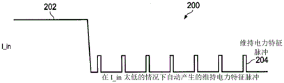
Fig. 2 is a diagram of an MPS pulse automatically generated in case i_in is too low.
Fig. 3 is a schematic block diagram of a system according to an example embodiment.
Fig. 4 is a schematic diagram of a first embodiment.
Fig. 5 is a schematic diagram of a second embodiment.
Fig. 6 shows the LED load of the PD.
Detailed Description
In the described example, circuitry within the PD automatically determines the need for an MPS signal without the need for an externally generated signal, and provides MPS pulses to maintain power to the PD while minimizing power consumption.
Fig. 1 shows a conventional system 100. Power flows from the PSE through the PD front end 102 to the PD system 104 and capacitor 110, which are part of a load (not shown). The power flowing to the load is controlled by PoE heat exchange switch 108. If the load current is less than the current required to maintain power from the PSE to the PD, external circuitry (not shown) generates an MPS signal that is supplied to the circuit 106 to cause the circuit 106 to generate a maintain power current pulse on the input line from the PSE. The externally generated pulses may be generated by a microprocessor located in an integrated circuit separate from the PD interface circuit (PD front end circuit 102), thus requiring additional integrated circuits. This adds cost to the end user and it adds complexity because the end user now must provide a circuit that measures power consumption and generates the MPS signal in a manner that minimizes the power consumed by the measuring device, such as a resistive shunt. One conventional technique receives a signal from an application circuit when a user presses a button to sleep an IP phone. The MPS pulse is generated until it receives a wake-up signal that is also generated from the user pressing a button.
Fig. 2 shows a waveform 200 of an input current to a PD. In fig. 2, when the current i_in 202 falls below the value required to maintain power to the PD, MPS pulses having a certain magnitude, duration, and pulse frequency are automatically generated according to aspects of the example embodiment, as shown at 204.
Fig. 3 is a schematic block diagram of a system 300 within a PD. In fig. 3, block 306 contains the circuitry shown in more detail in fig. 4 and 5. The PD receives power from the PSE along two or four of the four pairs of wires within the ethernet cable (labeled 302 and 304). The capacitor and zener diode combat voltage spikes. At start-up, the PSE looks for a resistor Rdet that is used to determine if an effective resistance (defined by the IEEE standard) is detected, which indicates that the PD is requesting power from the PSE. The PSE then increases the voltage and determines the amount of current drawn through resistor Rcls, which determines how much power should be provided as defined by the IEEE standard. By pulling RTN to operating voltage in a controlled manner after increasing the input voltageVss to turn on DC-to-DC converter 308 to control the inrush current, as with all heat exchange devices. The current is then allowed to reach its full current limit. A "power good" signal is provided at terminal PG. The DC/DC converter 308 (fig. 3) may not be part of the PD interface circuit, but rather be used to provide a controlled voltage to a load. For example, such a load may be an LED lighting device. Capacitor Cbulk is used by the DC-to-DC converter during start-up and is used to let the voltage V to the converter DD The input remains stable.
Fig. 4 shows an embodiment of a circuit 400 (which is shown as 306 in fig. 3, but the circuit 306 may have other functions not shown). Fig. 4 has a current limiting amplifier U1 with its non-inverting input coupled to a current limiting reference (not shown) and its inverting input coupled to a node between FET transistor Q1 and sense resistor Rsense. The other terminal of the transistor Q1 is connected to the return voltage RTN, and the other terminal of the sense resistor is connected to V SS . Current from the load of the PD flows through the RTN to V SS Thereby creating a voltage drop across Rsense for measuring the load current. If the voltage across the resistor exceeds a predetermined reference (current limit reference), then the load current is limited using transistor Q1.
The node between transistor Q1 and resistor Rsense is also coupled to the non-inverting input of comparator U2. The inverting input of comparator U2 is coupled to an automated MPS reference (not shown). If the voltage across resistor Rsense drops below the automatic MPS reference, comparator U2 provides a signal to sequential logic 406, which sequential logic 406 in turn provides an enable signal to amplifier U3. The non-inverting input of amplifier U3 is coupled to an MPS current reference (not shown) and its inverting input is coupled to the node between transistor Q3 and resistor Rext. The other terminal of the transistor Q3 is connected to V DD And the other terminal of the resistor Rext is connected to V SS . The oscillator OSC1 402 generates a signal that is converted to pulses by MPS pulse generator 404 to control timing logic 406 to generate MPS characteristic pulses required to maintain the PSE to the PD. These pulse-controlled amplifiers U3 generate a voltage at the node between the transistor and the external resistor Rext. Value determination of external resistorPass resistor Rext slave V DD Draw to V SS To provide MPS signals to the PSE. The resistor Rext may be external to the integrated circuit (e.g., 306) and thus may be used by an end user to determine the amount of current required to maintain power to the PD for that particular application.
Fig. 5 shows another embodiment of a circuit 500 (which is shown as 306 in fig. 3, but circuit 306 may have other functions not shown). In FIG. 5, a transistor Q1 is coupled between the return line RTN and a resistor R1, the other terminal of the resistor R1 is connected to V SS . The switch S1 connects the gate of the transistor Q1 and the output of the error amplifier U1. The non-inverting terminal of error amplifier U1 is coupled to a current limit reference (not shown) and its inverting input is coupled to the node between transistor Q1 and resistor R1. Error amplifier U1 measures the voltage across resistor R1 to determine if the current exceeds the maximum current limit and adjusts the current to that maximum limit. The transistor Q2 is coupled between the signal line RTN and the resistor R2, and the other terminal of the resistor R2 is coupled to a node between the transistor Q1 and the resistor R1. The node is also connected to the non-inverting input of comparator U2, the inverting input of comparator U2 being connected to an automatic MPS reference (not shown). Switch S2 is coupled between the output of error amplifier U1 and the gate of transistor Q2. Switch S4 is coupled to the gate of transistor Q2 and V SS Between them. Transistor Q3 is connected to voltage V DD And between the node between the transistor Q2 and the resistor R2. The gate of transistor Q3 is connected to the output of error amplifier U3, the non-inverting input of error amplifier U3 is connected to the MPS reference (not shown) and its inverting input is coupled to the node between transistor Q2 and resistor R2.
The output of comparator U2 is coupled to sequential logic 506, sequential logic 506 having an output for each of switches S1-S4 and an enable output coupled to the enable input of error amplifier U3. The oscillator OSC1 502 generates a signal that is converted to pulses by the MPS pulse generator 504, which are applied to the timing logic 506. The sequential logic uses a clock to generate control signals for switches S1-S4 and for pulses generated by error amplifier U3 and transistor Q3.
In normal operation, switches S1 and S4 are closed and switches S3 and S2 are open. In low power operation, switches S2 and S3 are closed and switches S1 and S4 are open, so the current limiting action of error amplifier U1 is active, as current limiting must always be provided. In normal operation, switch S4 is normally closed to maintain transistor Q2 off, and switch S1 is closed to allow U1 to control the current through Q1. The switches S2 and S3 are now open. All current from the load returns to the RTN node and through transistor Q1 and resistor R1. The voltage across resistor R1 is used to measure the current through the load and is applied to the inverting input of error amplifier U1. The current limit reference is applied to the non-inverting input of the error amplifier U1. This current measurement is used to limit the current if it exceeds a predetermined threshold. The voltage across resistor R1 is also compared to an automatic MPS reference applied to the inverting input of comparator U2, the output of comparator U2 being used to control sequential logic control switches S1 to S4. If the current through resistor R1 falls below a predetermined threshold, switches S1 and S4 are opened and switches S2 and S3 are closed by a signal generated by sequential logic 506. This turns off transistor Q1 and turns on transistor Q2. Thus, the current returned from the PD load through the RTN node passes through transistor Q2, through resistor R2, and then through resistor R1 to V SS 。
To minimize power dissipation, the value of resistor R1 is kept as low as possible. However, at low currents, this creates a large error due to any offset voltage of comparator U2 when U2 is used to compare the load current to a threshold (automatic MPS reference). For example, with R1 having a value of 25mΩ, a 1mV offset in comparator U2 may form a measurement error of 40 mA. The normal current required to maintain power from the PSE to the PD is quite low (only 10mA to 15 mA), so this can be a significant error. In the circuit of fig. 5, the second resistor R2 is switched into the circuit upon determining that the current is too low to maintain power from the PSE to the PD. For example, this resistor may be 5Ω. This resistor is used by U3 along with resistor R1 in series to generate any desired MPS current. This much larger resistance allows the U3 to control the MPS current much more accurately, producing only the extra current needed. For example, with a 1mV offset in amplifier U3, the error would be only 200 μA. Thus, this circuit permits the utilization of a low resistance shunt to minimize power loss in the shunt resistor during normal operation, and then adds a higher resistance to generate the more accurate current pulses needed to maintain power flow from the PSE to the PD, thus saving power.
If an MPS pulse is required, then the timing logic 506 enables the enable input of the error amplifier U3 to generate a voltage via transistor Q3 at the top of the resistor chain including R2 and R1, which determines that a pass circuit is required in order to be supplied to V DD The pulses of (2) meet or exceed the required amount of additional current of the MPS characteristic so that the PSE will continue to provide power to the PD. The load current also flows through R1 and R2, and thus it is included in the current generated by U3, thus generating only the additional current needed to meet MPS requirements.
Fig. 6 shows one type of load 600 for a DC/DC converter, such as the DC/DC converter 308 of fig. 3. As shown in fig. 6, the load includes a plurality of LEDs, such as 602a, 602 b..602 n, that connect the Vout terminal from the converter to ground, for example. The number of LEDs in the string is a design choice. For example, the LED may provide general room lighting while indicating that power is being supplied to a device such as the PD itself. Other circuits may provide additional functionality, such as determining (by a motion detector) occupancy of an area and may also be connected as part of a load.
Modifications are possible in the described embodiments and other embodiments are possible within the scope of the claims.
Claims (18)
1. A power receiving apparatus PD, the PD apparatus comprising:
a first voltage supply terminal and a second voltage supply terminal;
a return terminal;
a comparator coupled to the first resistor, current flowing from the return terminal through the first resistor to the second voltage supply terminal to generate a voltage drop across the first resistor, and the comparator configured to generate an MPS enable signal in response to detecting that the voltage drop across the first resistor is less than a first sustain power feature MPS reference threshold; and
a first amplifier configured to generate a load pulse required to maintain power by a power sourcing equipment PSE to the PD device based on a second MPS reference threshold in response to receiving the MPS enable signal.
2. The PD apparatus of claim 1, wherein:
the first voltage supply terminal is configured to receive a first voltage V from the PSE of a power over ethernet PoE system DD ;
The second voltage supply terminal is configured to receive a second voltage V from the PSE of the PoE system SS The method comprises the steps of carrying out a first treatment on the surface of the And is also provided with
The return terminal is configured to receive a ground voltage from a load of the powered device.
3. The PD device of claim 1, further comprising:
a first transistor coupled between the return terminal and a sense terminal configured to provide a sense voltage representative of the current,
wherein the comparator has a non-inverting input coupled to the sense terminal, an inverting input configured to receive the first MPS reference threshold, and an output configured to output the MPS enable signal.
4. The PD apparatus according to claim 3, wherein:
the first resistor is coupled between the sense terminal and the second voltage supply terminal.
5. The PD device of claim 4, further comprising:
a second amplifier having a non-inverting input configured to receive a current limit reference, an inverting input coupled to the sense terminal, and an output coupled to a control terminal of the first transistor.
6. The PD device of claim 3, further comprising:
a second transistor coupled between the first voltage supply terminal and an MPS terminal configured to output the MPS pulse; and
a second resistor coupled between the MPS terminal and the second voltage supply terminal, wherein the first amplifier has a non-inverting input configured to receive the second MPS reference threshold, an inverting input coupled to the MPS terminal, and an output coupled to a control terminal of the second transistor.
7. The PD device of claim 1, further comprising:
a first stage coupled between the return terminal and the second voltage supply terminal and configured to generate a first sense voltage at a sense terminal representative of the current when the first stage is enabled;
a second stage coupled between the return terminal and the second voltage supply terminal and configured to generate a second sense voltage at the sense terminal representative of the current when the second stage is enabled; and
sequential logic configured to enable the first stage and disable the second stage when the MPS enable signal is absent, and configured to disable the first stage and enable the second stage when the MPS enable signal is generated.
8. The PD apparatus of claim 7, wherein:
the first stage includes a first transistor coupled between the return terminal and the sense terminal, and the first resistor coupled between the sense terminal and the second voltage supply terminal; and
the second stage includes a third transistor coupled between the return terminal and an MPS terminal, and a third resistor coupled between the MPS terminal and the sense terminal, the MPS terminal configured to output the MPS pulse.
9. The PD device of claim 8, further comprising:
a second amplifier having a non-inverting input configured to receive a current limit reference, an inverting input coupled to the sense terminal, and an output;
a first switch coupled between the output of the second amplifier and a control terminal of the first transistor, the first switch configured to be closed by the sequential logic in the absence of the MPS enable signal; and
a second switch coupled between the output of the second amplifier and a control terminal of the third transistor, the second switch configured to be closed by the sequential logic when generating the MPS enable signal.
10. The PD device of claim 9, further comprising:
a third switch coupled between the control terminal of the first transistor and the second voltage supply terminal, the third switch configured to be closed by the sequential logic when generating the MPS enable signal; and
a fourth switch coupled between the control terminal and the sense terminal of the third transistor, the fourth switch configured to be closed by the sequential logic in the absence of the MPS enable signal.
11. The PD device of claim 8, further comprising:
a second transistor coupled between the first voltage supply terminal and the MPS terminal; and is also provided with
Wherein the first amplifier has a non-inverting input configured to receive the second MPS reference threshold, an inverting input coupled to the MPS terminal, and an output coupled to a control terminal of the third transistor.
12. The PD apparatus of claim 7, wherein:
the comparator has a non-inverting input coupled to the sense terminal, an inverting input configured to receive the first MPS reference threshold, and an output configured to assert the MPS enable signal.
13. An integrated circuit, IC, for use in a powered device, PD, of a power over ethernet, poE, system, the IC comprising:
a first voltage supply terminal and a second voltage supply terminal;
a return terminal;
a first transistor coupled between the return terminal and a sense terminal configured to provide a sense voltage representative of a current between the return terminal and the second voltage supply terminal; and
a comparator having a non-inverting input coupled to the sense terminal, an inverting input configured to receive a first sustained power characteristic MPS reference threshold, and an output configured to output an MPS enable signal; and
a first amplifier configured to generate a load pulse required to maintain power by a power sourcing equipment PSE to the PD device based on a second MPS reference threshold in response to receiving the MPS enable signal.
14. The IC of claim 13, further comprising:
a first resistor coupled between the sense terminal and the second voltage supply terminal;
a second amplifier includes a non-inverting input configured to receive a current limit reference, an inverting input coupled to the sense terminal, and an output coupled to a control terminal of the first transistor.
15. The IC of claim 13, further comprising:
a second transistor coupled between the first voltage supply terminal and an MPS terminal configured to output the MPS pulse; and
a second resistor coupled between the MPS terminal and the second voltage supply terminal;
wherein the first amplifier has a non-inverting input configured to receive the second MPS reference threshold, an inverting input coupled to the MPS terminal, and an output coupled to a control terminal of the second transistor.
16. An integrated circuit, IC, for use in a powered device, PD, of a power over ethernet, poE, system, the IC comprising:
a first voltage supply terminal and a second voltage supply terminal associated with the PoE system;
a return terminal;
a first stage comprising a first transistor coupled between the return terminal and a sense terminal, and a first resistor coupled between the sense terminal and the second voltage supply terminal;
a second stage comprising a second transistor coupled between the return terminal and a sustain power signature MPS terminal, and a second resistor coupled between the MPS terminal and the sense terminal;
a comparator configured to assert a MPS enable signal in response to a sense voltage at the sense terminal being less than a first MPS reference threshold;
sequential logic configured to enable the first stage and disable the second stage when the MPS enable signal is not asserted, and configured to disable the first stage and enable the second stage when the MPS enable signal is asserted; and
a first amplifier configured to generate a load pulse required to maintain power by a power sourcing equipment PSE to the PD device based on a second MPS reference threshold in response to receiving the MPS enable signal.
17. The IC of claim 16, further comprising:
a second amplifier having a non-inverting input configured to receive a current limit reference, an inverting input coupled to the sense terminal, and an output;
a first switch coupled between the output of the second amplifier and a control terminal of the first transistor, the first switch configured to be closed by the sequential logic when the MPS enable signal is not asserted;
a second switch coupled between the output of the second amplifier and a control terminal of the second transistor, the second switch configured to be closed by the sequential logic when the MPS enable signal is asserted;
a third switch coupled between the control terminal of the first transistor and the second voltage supply terminal, the third switch configured to be closed by the sequential logic when the MPS enable signal is asserted; and
a fourth switch coupled between the control terminal and the sense terminal of the second transistor, the fourth switch configured to be closed by the sequential logic when the MPS enable signal is not asserted.
18. The IC of claim 16, further comprising:
a third transistor coupled between the first voltage supply terminal and the MPS terminal;
wherein the first amplifier includes a non-inverting input configured to receive the second MPS reference threshold, an inverting input coupled to the MPS terminal, and an output coupled to a control terminal of the third transistor.
Priority Applications (1)
| Application Number | Priority Date | Filing Date | Title |
|---|---|---|---|
| CN202010310923.2A CN111478777B (en) | 2014-09-29 | 2015-09-29 | Power over Ethernet powered device automatically maintains power characteristics |
Applications Claiming Priority (7)
| Application Number | Priority Date | Filing Date | Title |
|---|---|---|---|
| US201462057028P | 2014-09-29 | 2014-09-29 | |
| US62/057,028 | 2014-09-29 | ||
| US14/867,635 | 2015-09-28 | ||
| US14/867,635 US10057959B2 (en) | 2014-09-29 | 2015-09-28 | Power over ethernet powered device having automatic power signature |
| CN201580043564.6A CN106576048B (en) | 2014-09-29 | 2015-09-29 | Power over ethernet powered device auto-sustain power feature |
| CN202010310923.2A CN111478777B (en) | 2014-09-29 | 2015-09-29 | Power over Ethernet powered device automatically maintains power characteristics |
| PCT/US2015/053053 WO2016054120A1 (en) | 2014-09-29 | 2015-09-29 | Power over ethernet powered device automatic maintaining power signature |
Related Parent Applications (1)
| Application Number | Title | Priority Date | Filing Date |
|---|---|---|---|
| CN201580043564.6A Division CN106576048B (en) | 2014-09-29 | 2015-09-29 | Power over ethernet powered device auto-sustain power feature |
Publications (2)
| Publication Number | Publication Date |
|---|---|
| CN111478777A CN111478777A (en) | 2020-07-31 |
| CN111478777B true CN111478777B (en) | 2023-07-07 |
Family
ID=55586020
Family Applications (2)
| Application Number | Title | Priority Date | Filing Date |
|---|---|---|---|
| CN202010310923.2A Active CN111478777B (en) | 2014-09-29 | 2015-09-29 | Power over Ethernet powered device automatically maintains power characteristics |
| CN201580043564.6A Active CN106576048B (en) | 2014-09-29 | 2015-09-29 | Power over ethernet powered device auto-sustain power feature |
Family Applications After (1)
| Application Number | Title | Priority Date | Filing Date |
|---|---|---|---|
| CN201580043564.6A Active CN106576048B (en) | 2014-09-29 | 2015-09-29 | Power over ethernet powered device auto-sustain power feature |
Country Status (5)
| Country | Link |
|---|---|
| US (2) | US10057959B2 (en) |
| EP (1) | EP3221999B1 (en) |
| JP (2) | JP6617149B2 (en) |
| CN (2) | CN111478777B (en) |
| WO (1) | WO2016054120A1 (en) |
Families Citing this family (11)
| Publication number | Priority date | Publication date | Assignee | Title |
|---|---|---|---|---|
| US10057959B2 (en) | 2014-09-29 | 2018-08-21 | Texas Instruments Incorporated | Power over ethernet powered device having automatic power signature |
| US10153909B2 (en) * | 2015-07-06 | 2018-12-11 | Silicon Laboratories Inc. | Power over ethernet powered device configured for low duty-cycle operation |
| EP3338403B1 (en) * | 2015-08-20 | 2018-12-05 | Philips Lighting Holding B.V. | Power source equipment device for a power of ethernet lighting system |
| US10263794B2 (en) * | 2016-05-19 | 2019-04-16 | Linear Technology Corporation | Maintain power signature controller at power interface of PoE or PoDL system |
| US10432413B2 (en) * | 2017-02-07 | 2019-10-01 | Texas Instruments Incorporated | Automatic power over ethernet pulse width signaling correction |
| WO2019202583A1 (en) * | 2018-04-16 | 2019-10-24 | Microsemi P.O.E Ltd. | Mark and hold system and method |
| US11240061B2 (en) | 2019-06-03 | 2022-02-01 | Progress Rail Locomotive Inc. | Methods and systems for controlling locomotives |
| CN113125877B (en) * | 2021-03-02 | 2022-12-06 | 华为技术有限公司 | PD detection equipment for powered device |
| CN113726530B (en) * | 2021-07-12 | 2022-07-12 | 西安电子科技大学 | Ethernet power supply system |
| CN113885638B (en) * | 2021-12-08 | 2022-02-11 | 杭州杰为科技有限公司 | Pd circuit for increasing mps function and method for increasing mps function on pd circuit |
| US20240036625A1 (en) * | 2022-07-28 | 2024-02-01 | Microchip Technology Incorporated | POE PSE MPS Support for PSE Voltage Transients |
Citations (3)
| Publication number | Priority date | Publication date | Assignee | Title |
|---|---|---|---|---|
| CN103200014A (en) * | 2011-12-20 | 2013-07-10 | 马克西姆综合产品公司 | Maintain power signature (MPS) powered device (PD) |
| CN103888272A (en) * | 2012-09-27 | 2014-06-25 | 马克西姆综合产品公司 | Maintain power signature (mps) from a powered device (pd) while power is drawn from another source |
| CN104009630A (en) * | 2013-02-22 | 2014-08-27 | 德州仪器公司 | Emulated current ramp for DC-DC converter |
Family Cites Families (26)
| Publication number | Priority date | Publication date | Assignee | Title |
|---|---|---|---|---|
| CN101201692B (en) * | 2002-10-18 | 2010-06-16 | 汤姆森许可贸易公司 | Peripheral equipment having bus control power switch for operating power supply |
| JP2005006444A (en) * | 2003-06-13 | 2005-01-06 | Japan Aviation Electronics Industry Ltd | Power supply device for illumination lamp |
| US7639469B2 (en) * | 2005-01-25 | 2009-12-29 | Linear Technology Corporation | Power sourcing equipment having auto-zero circuit for determining and controlling output current |
| CN101371492B (en) * | 2006-01-17 | 2012-08-15 | 美国博通公司 | Power over Ethernet controller and method for detecting and classifying power supply equipment |
| US8205099B2 (en) | 2006-04-07 | 2012-06-19 | Broadcom Corporation | Power over Ethernet connector with integrated power source equipment (PSE) controller |
| US8149858B2 (en) | 2007-01-05 | 2012-04-03 | Broadcom Corporation | Powered device analysis and power control in a power-over-ethernet system |
| JP2009200146A (en) * | 2008-02-20 | 2009-09-03 | Sharp Corp | Led drive circuit and led illumination apparatus using it |
| JP4636102B2 (en) * | 2008-03-24 | 2011-02-23 | 東芝ライテック株式会社 | Power supply device and lighting fixture |
| TWM354157U (en) * | 2008-10-30 | 2009-04-01 | Silitek Electronic Guangzhou | Power supply apparatus |
| US8081495B2 (en) * | 2008-11-20 | 2011-12-20 | Semiconductor Components Industries, Llc | Over power compensation in switched mode power supplies |
| CA2770225A1 (en) * | 2009-08-07 | 2011-02-10 | Led Roadway Lighting Ltd. | Single-ended primary inductance converter (sepic) based power supply for driving multiple strings of light emitting diodes (leds) in roadway lighting fixtures |
| US8581438B2 (en) * | 2009-11-23 | 2013-11-12 | Linear Technology Corporation | Providing power to powered device having multiple power supply inputs |
| US8947157B2 (en) * | 2010-04-20 | 2015-02-03 | Rf Micro Devices, Inc. | Voltage multiplier charge pump buck |
| KR101775162B1 (en) * | 2010-06-28 | 2017-09-05 | 로무 가부시키가이샤 | Load driving circuit, light emitting apparatus using the same and display device |
| US8868946B2 (en) | 2010-09-08 | 2014-10-21 | Texas Instruments Incorporated | Maintaining power to a powered device during a low power mode of the powered device |
| CN102457384A (en) * | 2010-10-28 | 2012-05-16 | 鸿富锦精密工业(深圳)有限公司 | Power device |
| US20130073874A1 (en) | 2011-09-19 | 2013-03-21 | Ali Eghbal | Interface apparatus and method for ethernet powered device |
| JP6145825B2 (en) * | 2012-05-28 | 2017-06-14 | パナソニックIpマネジメント株式会社 | Light emitting diode drive device and semiconductor device |
| CN104541575B (en) * | 2012-08-07 | 2017-02-22 | 皇家飞利浦有限公司 | power distribution system |
| GB2505247A (en) | 2012-08-24 | 2014-02-26 | Zeta Specialist Lighting Ltd | DC powered lighting via Power over Ethernet cables |
| WO2014033575A1 (en) * | 2012-08-29 | 2014-03-06 | Koninklijke Philips N.V. | Method and apparatus for multiplexed power and data supply via a two-wire data communication cable |
| WO2014080337A2 (en) * | 2012-11-26 | 2014-05-30 | Koninklijke Philips N.V. | Signal-level based control of power grid load systems |
| JP6247455B2 (en) * | 2013-05-17 | 2017-12-13 | ローム株式会社 | LIGHT EMITTING ELEMENT DRIVE CIRCUIT, AND LIGHT EMITTING DEVICE AND ELECTRONIC DEVICE USING THE SAME |
| WO2015106992A1 (en) | 2014-01-14 | 2015-07-23 | Koninklijke Philips N.V. | Low power standby for a powered device in a power distribution system |
| US20150365003A1 (en) * | 2014-06-12 | 2015-12-17 | Laurence P. Sadwick | Power Conversion System |
| US10057959B2 (en) | 2014-09-29 | 2018-08-21 | Texas Instruments Incorporated | Power over ethernet powered device having automatic power signature |
-
2015
- 2015-09-28 US US14/867,635 patent/US10057959B2/en active Active
- 2015-09-29 CN CN202010310923.2A patent/CN111478777B/en active Active
- 2015-09-29 JP JP2017536235A patent/JP6617149B2/en active Active
- 2015-09-29 CN CN201580043564.6A patent/CN106576048B/en active Active
- 2015-09-29 WO PCT/US2015/053053 patent/WO2016054120A1/en active Application Filing
- 2015-09-29 EP EP15846625.0A patent/EP3221999B1/en active Active
-
2018
- 2018-07-17 US US16/037,465 patent/US10327305B2/en active Active
-
2019
- 2019-11-11 JP JP2019203936A patent/JP6792046B2/en active Active
Patent Citations (3)
| Publication number | Priority date | Publication date | Assignee | Title |
|---|---|---|---|---|
| CN103200014A (en) * | 2011-12-20 | 2013-07-10 | 马克西姆综合产品公司 | Maintain power signature (MPS) powered device (PD) |
| CN103888272A (en) * | 2012-09-27 | 2014-06-25 | 马克西姆综合产品公司 | Maintain power signature (mps) from a powered device (pd) while power is drawn from another source |
| CN104009630A (en) * | 2013-02-22 | 2014-08-27 | 德州仪器公司 | Emulated current ramp for DC-DC converter |
Also Published As
| Publication number | Publication date |
|---|---|
| CN106576048A (en) | 2017-04-19 |
| EP3221999A1 (en) | 2017-09-27 |
| JP6792046B2 (en) | 2020-11-25 |
| CN111478777A (en) | 2020-07-31 |
| US20180324910A1 (en) | 2018-11-08 |
| JP2017533529A (en) | 2017-11-09 |
| CN106576048B (en) | 2020-05-15 |
| EP3221999B1 (en) | 2022-04-20 |
| EP3221999A4 (en) | 2018-06-27 |
| JP2020042833A (en) | 2020-03-19 |
| US10057959B2 (en) | 2018-08-21 |
| US20160095175A1 (en) | 2016-03-31 |
| JP6617149B2 (en) | 2019-12-11 |
| US10327305B2 (en) | 2019-06-18 |
| WO2016054120A1 (en) | 2016-04-07 |
Similar Documents
| Publication | Publication Date | Title |
|---|---|---|
| CN111478777B (en) | Power over Ethernet powered device automatically maintains power characteristics | |
| US8667310B2 (en) | Circuit for indicating power level over a communication interface | |
| CA3015814C (en) | Active/ieee standards based power over ethernet low standby power circuit architecture | |
| US9780955B2 (en) | Power over ethernet method and apparatus for immediate power availability | |
| CN107210921B (en) | POE power utilization device and method | |
| US20080238447A1 (en) | Isolated capacitive signature detection for powered devices | |
| JP2008529362A (en) | System for providing power through a communication cable having a mechanism for determining the resistance of the communication cable | |
| US10153909B2 (en) | Power over ethernet powered device configured for low duty-cycle operation | |
| US10659241B2 (en) | Automatic power over ethernet pulse width signaling correction | |
| US9927779B2 (en) | Power sourcing equipment and method of detecting inrush fault errors | |
| CN107810618B (en) | Forced large-capacity capacitor discharge in a powered device | |
| US8149602B2 (en) | Method and apparatus for detecting end of start up phase | |
| CN109844547A (en) | Current monitor circuit | |
| CN113037508B (en) | Power-down control circuit and power-down control method |
Legal Events
| Date | Code | Title | Description |
|---|---|---|---|
| PB01 | Publication | ||
| PB01 | Publication | ||
| SE01 | Entry into force of request for substantive examination | ||
| SE01 | Entry into force of request for substantive examination | ||
| GR01 | Patent grant | ||
| GR01 | Patent grant |