CN111279460A - Dry etching method - Google Patents
Dry etching method Download PDFInfo
- Publication number
- CN111279460A CN111279460A CN201880068626.2A CN201880068626A CN111279460A CN 111279460 A CN111279460 A CN 111279460A CN 201880068626 A CN201880068626 A CN 201880068626A CN 111279460 A CN111279460 A CN 111279460A
- Authority
- CN
- China
- Prior art keywords
- acid
- fluorine
- carboxylic acid
- containing carboxylic
- dry etching
- Prior art date
- Legal status (The legal status is an assumption and is not a legal conclusion. Google has not performed a legal analysis and makes no representation as to the accuracy of the status listed.)
- Granted
Links
Images

Classifications
-
- H—ELECTRICITY
- H01—ELECTRIC ELEMENTS
- H01L—SEMICONDUCTOR DEVICES NOT COVERED BY CLASS H10
- H01L21/00—Processes or apparatus adapted for the manufacture or treatment of semiconductor or solid state devices or of parts thereof
- H01L21/02—Manufacture or treatment of semiconductor devices or of parts thereof
- H01L21/04—Manufacture or treatment of semiconductor devices or of parts thereof the devices having at least one potential-jump barrier or surface barrier, e.g. PN junction, depletion layer or carrier concentration layer
- H01L21/18—Manufacture or treatment of semiconductor devices or of parts thereof the devices having at least one potential-jump barrier or surface barrier, e.g. PN junction, depletion layer or carrier concentration layer the devices having semiconductor bodies comprising elements of Group IV of the Periodic System or AIIIBV compounds with or without impurities, e.g. doping materials
- H01L21/30—Treatment of semiconductor bodies using processes or apparatus not provided for in groups H01L21/20 - H01L21/26
- H01L21/31—Treatment of semiconductor bodies using processes or apparatus not provided for in groups H01L21/20 - H01L21/26 to form insulating layers thereon, e.g. for masking or by using photolithographic techniques; After treatment of these layers; Selection of materials for these layers
- H01L21/3105—After-treatment
- H01L21/311—Etching the insulating layers by chemical or physical means
- H01L21/31105—Etching inorganic layers
- H01L21/31111—Etching inorganic layers by chemical means
- H01L21/31116—Etching inorganic layers by chemical means by dry-etching
-
- C—CHEMISTRY; METALLURGY
- C09—DYES; PAINTS; POLISHES; NATURAL RESINS; ADHESIVES; COMPOSITIONS NOT OTHERWISE PROVIDED FOR; APPLICATIONS OF MATERIALS NOT OTHERWISE PROVIDED FOR
- C09K—MATERIALS FOR MISCELLANEOUS APPLICATIONS, NOT PROVIDED FOR ELSEWHERE
- C09K13/00—Etching, surface-brightening or pickling compositions
- C09K13/04—Etching, surface-brightening or pickling compositions containing an inorganic acid
- C09K13/08—Etching, surface-brightening or pickling compositions containing an inorganic acid containing a fluorine compound
-
- C—CHEMISTRY; METALLURGY
- C23—COATING METALLIC MATERIAL; COATING MATERIAL WITH METALLIC MATERIAL; CHEMICAL SURFACE TREATMENT; DIFFUSION TREATMENT OF METALLIC MATERIAL; COATING BY VACUUM EVAPORATION, BY SPUTTERING, BY ION IMPLANTATION OR BY CHEMICAL VAPOUR DEPOSITION, IN GENERAL; INHIBITING CORROSION OF METALLIC MATERIAL OR INCRUSTATION IN GENERAL
- C23F—NON-MECHANICAL REMOVAL OF METALLIC MATERIAL FROM SURFACE; INHIBITING CORROSION OF METALLIC MATERIAL OR INCRUSTATION IN GENERAL; MULTI-STEP PROCESSES FOR SURFACE TREATMENT OF METALLIC MATERIAL INVOLVING AT LEAST ONE PROCESS PROVIDED FOR IN CLASS C23 AND AT LEAST ONE PROCESS COVERED BY SUBCLASS C21D OR C22F OR CLASS C25
- C23F1/00—Etching metallic material by chemical means
- C23F1/10—Etching compositions
- C23F1/12—Gaseous compositions
-
- H—ELECTRICITY
- H01—ELECTRIC ELEMENTS
- H01L—SEMICONDUCTOR DEVICES NOT COVERED BY CLASS H10
- H01L21/00—Processes or apparatus adapted for the manufacture or treatment of semiconductor or solid state devices or of parts thereof
- H01L21/02—Manufacture or treatment of semiconductor devices or of parts thereof
- H01L21/02104—Forming layers
- H01L21/02107—Forming insulating materials on a substrate
- H01L21/02109—Forming insulating materials on a substrate characterised by the type of layer, e.g. type of material, porous/non-porous, pre-cursors, mixtures or laminates
- H01L21/02112—Forming insulating materials on a substrate characterised by the type of layer, e.g. type of material, porous/non-porous, pre-cursors, mixtures or laminates characterised by the material of the layer
- H01L21/02123—Forming insulating materials on a substrate characterised by the type of layer, e.g. type of material, porous/non-porous, pre-cursors, mixtures or laminates characterised by the material of the layer the material containing silicon
- H01L21/0217—Forming insulating materials on a substrate characterised by the type of layer, e.g. type of material, porous/non-porous, pre-cursors, mixtures or laminates characterised by the material of the layer the material containing silicon the material being a silicon nitride not containing oxygen, e.g. SixNy or SixByNz
-
- H—ELECTRICITY
- H01—ELECTRIC ELEMENTS
- H01L—SEMICONDUCTOR DEVICES NOT COVERED BY CLASS H10
- H01L21/00—Processes or apparatus adapted for the manufacture or treatment of semiconductor or solid state devices or of parts thereof
- H01L21/02—Manufacture or treatment of semiconductor devices or of parts thereof
- H01L21/02104—Forming layers
- H01L21/02365—Forming inorganic semiconducting materials on a substrate
- H01L21/02518—Deposited layers
- H01L21/02521—Materials
- H01L21/02524—Group 14 semiconducting materials
- H01L21/02532—Silicon, silicon germanium, germanium
-
- H—ELECTRICITY
- H01—ELECTRIC ELEMENTS
- H01L—SEMICONDUCTOR DEVICES NOT COVERED BY CLASS H10
- H01L21/00—Processes or apparatus adapted for the manufacture or treatment of semiconductor or solid state devices or of parts thereof
- H01L21/02—Manufacture or treatment of semiconductor devices or of parts thereof
- H01L21/02104—Forming layers
- H01L21/02365—Forming inorganic semiconducting materials on a substrate
- H01L21/02518—Deposited layers
- H01L21/02587—Structure
- H01L21/0259—Microstructure
- H01L21/02595—Microstructure polycrystalline
-
- H—ELECTRICITY
- H01—ELECTRIC ELEMENTS
- H01L—SEMICONDUCTOR DEVICES NOT COVERED BY CLASS H10
- H01L21/00—Processes or apparatus adapted for the manufacture or treatment of semiconductor or solid state devices or of parts thereof
- H01L21/02—Manufacture or treatment of semiconductor devices or of parts thereof
- H01L21/04—Manufacture or treatment of semiconductor devices or of parts thereof the devices having at least one potential-jump barrier or surface barrier, e.g. PN junction, depletion layer or carrier concentration layer
- H01L21/18—Manufacture or treatment of semiconductor devices or of parts thereof the devices having at least one potential-jump barrier or surface barrier, e.g. PN junction, depletion layer or carrier concentration layer the devices having semiconductor bodies comprising elements of Group IV of the Periodic System or AIIIBV compounds with or without impurities, e.g. doping materials
- H01L21/30—Treatment of semiconductor bodies using processes or apparatus not provided for in groups H01L21/20 - H01L21/26
- H01L21/302—Treatment of semiconductor bodies using processes or apparatus not provided for in groups H01L21/20 - H01L21/26 to change their surface-physical characteristics or shape, e.g. etching, polishing, cutting
- H01L21/306—Chemical or electrical treatment, e.g. electrolytic etching
- H01L21/3065—Plasma etching; Reactive-ion etching
-
- H—ELECTRICITY
- H01—ELECTRIC ELEMENTS
- H01L—SEMICONDUCTOR DEVICES NOT COVERED BY CLASS H10
- H01L21/00—Processes or apparatus adapted for the manufacture or treatment of semiconductor or solid state devices or of parts thereof
- H01L21/67—Apparatus specially adapted for handling semiconductor or electric solid state devices during manufacture or treatment thereof; Apparatus specially adapted for handling wafers during manufacture or treatment of semiconductor or electric solid state devices or components ; Apparatus not specifically provided for elsewhere
- H01L21/67005—Apparatus not specifically provided for elsewhere
- H01L21/67011—Apparatus for manufacture or treatment
- H01L21/67017—Apparatus for fluid treatment
- H01L21/67063—Apparatus for fluid treatment for etching
- H01L21/67069—Apparatus for fluid treatment for etching for drying etching
Abstract
The present invention provides a dry etching method characterized by etching silicon nitride by bringing a mixed gas containing hydrogen fluoride and a fluorine-containing carboxylic acid into contact with the silicon nitride at a temperature of less than 100 ℃ without plasma. The amount of the fluorine-containing carboxylic acid is preferably 0.01 vol% or more of the total amount of the hydrogen fluoride and the fluorine-containing carboxylic acid. Examples of the fluorine-containing carboxylic acid include monofluoroacetic acid, difluoroacetic acid, trifluoroacetic acid, difluoropropionic acid, pentafluoropropionic acid, and pentafluorobutyric acid. By the dry etching method, silicon nitride can be etched at a high etching rate, and silicon oxide and polysilicon have a high selectivity ratio, and damage to silicon oxide can be suppressed.
Description
Technical Field
The present invention relates to a dry etching method using a gas containing HF and using silicon nitride (SiN) as an etching target.
Background
In the manufacture of semiconductor devices, a silicon nitride (hereinafter referred to as SiN) and a silicon oxide (hereinafter referred to as SiO) may be formed on a single-crystal silicon substrate2) And/or a process of selectively etching SiN in a structure adjacent to polycrystalline silicon (hereinafter referred to as p-Si).
As an etching method of SiN, wet etching using hot phosphoric acid or etching using CF is known4Dry etching of plasma generated from the compound gas.
For example, patent document 1 describes a dry etching method for forming SiO2SiN is selectively plasma etched in the presence of a silicide metal or silicon using a process comprising the formula: CH (CH)xF4-x(x represents 2 or 3) and an etching gas such as oxygen. Patent document 1 describes a self-SiO2The opening portion of the film selectively etches the SiN film and the p-Si film thereunder is used as an etching stopper.
However, in wet etching using hot phosphoric acid or dry etching using plasma, not only SiN but also SiO are etched2It is also etched, so that there is a difficulty in securing SiN with respect to SiO2The selection ratio of (a).
On the other hand, patent document 2 describes that an etching is performed on SiO by flowing HF gas in a plasma-free heating environment2Method of SiN film on film.
In addition, the SiO film is formed to solve the technical problem in the method described in patent document 22A method for reducing the etching rate of a SiN film on a film, and patent document 3 describes adding F to HF2A method of producing a gas.
However, when the SiN film is etched by HF gas as in patent document 2, SiO is formed2The membrane is also exposed to HF and NH as a reaction product3Etching, existence of SiN/SiO which could not be improved2The selection ratio of (a). Further, if F is added as in patent document 32Gas then existsp-Si by F2And the like, and a high SiN/Si selectivity cannot be obtained.
On the other hand, patent document 4 describes that a mixed gas of HF + NO is used for SiO2A method for etching a SiN film with a high selectivity by using a film and/or a p-Si film, and a method for suppressing SiO by adding NO gas as an etching gas (assist gas)2Damage to the membrane.
Documents of the prior art
Patent document
Patent document 1: japanese laid-open patent publication No. 8-59215
Patent document 2: japanese laid-open patent publication No. 2008-187105 (Japanese patent No. 4833878)
Patent document 3: japanese laid-open patent publication No. 2010-182730 (Japanese patent publication No. 5210191)
Patent document 4: japanese laid-open patent publication No. 2014-197603 (Japanese patent publication No. 6073172)
Disclosure of Invention
Technical problem to be solved by the invention
However, in patent document 4, even if the effect of increasing the selectivity of SiN can be obtained, NH is by-produced by etching SiN3Therefore, it is not possible to sufficiently suppress SiO2The damage of (2). In recent progress of miniaturization, slight surface roughness caused by such damage has become a problem which cannot be ignored, and improvement thereof has been desired.
In addition, to suppress SiO2The damage of (2) is considered to be the addition of N to an etching gas such as HF + NO2Or inert gas such as Ar or He. However, this method has a new problem in that the etching rate of SiN, which is originally the target, is greatly reduced. Therefore, in order to compensate for this low etching rate, a method of securing an etching amount by extending the treatment time of the etching step is also conceivable, but SiO2The time of exposure to the etching gas becomes long, resulting in SiO2The method of adding a diluent gas does not solve the problem of the progress of surface damage.
The object of the present invention is to provide a method for etching a semiconductor device with high etching rateEtch SiN at a rate to form semiconductor devices on a silicon substrate, for SiO2Or p-Si has a high selectivity ratio, and further, SiO can be inhibited2The damage dry etching method of (1).
Means for solving the problems
The inventors of the present invention have made intensive studies and as a result, found that a fluorine-containing carboxylic acid has: NH generated by HF by-product in the etching of SiN can be trapped3(ii) a Non-etching SiO2And p-Si; and does not interfere with the etching characteristics of SiN by HF, the above problems can be solved by etching SiN with a gas in which HF is mixed with the fluorocarboxylic acid, and the present invention has been completed.
Specifically, the present invention provides a dry etching method characterized by etching silicon nitride by bringing a mixed gas containing hydrogen fluoride and a fluorine-containing carboxylic acid into contact with the silicon nitride at a temperature of less than 100 ℃ without plasma.
Effects of the invention
The invention can provide a method for etching SiN with high etching rate to form SiO in semiconductor device on silicon substrate2And p-Si has a high selectivity ratio, and further, SiO can be inhibited2The damage dry etching method of (1).
Drawings
FIG. 1 is a schematic view of a reaction apparatus 1 used in examples and comparative examples.
Detailed Description
The present invention will be described in detail below, but the description of the constituent elements described below is only an example of the embodiment of the present invention, and the present invention is not limited to the specific contents described below. Various modifications can be made within the scope of the present invention.
In the dry etching method of the present invention, a mixed gas containing hydrogen fluoride and fluorine-containing carboxylic acid is used as a dry etching gas composition, and the dry etching gas composition is brought into contact with silicon nitride at a temperature of less than 100 ℃ without plasma to etch the silicon nitride.
The amount of the fluorine-containing carboxylic acid added to the mixed gas is preferably 0.01 vol% or more of the total amount of the hydrogen fluoride and the fluorine-containing carboxylic acid.
The upper limit of the amount to be added is naturally determined depending on the vapor pressure of each compound and the process pressure. That is, when the process pressure is lower than the vapor pressure of the fluorocarboxylic acid, the amount of fluorocarboxylic acid added increases, and the concentration of HF decreases, so that HF is insufficient and the etching rate of SiN cannot be sufficiently obtained. Therefore, the amount of addition is preferably only an amount at most such that the concentration ratio of HF to the fluorocarboxylic acid (HF/fluorocarboxylic acid) is 1 or more.
That is, the amount of the fluorine-containing carboxylic acid added to the mixed gas is preferably 0.01% by volume or more and 50% by volume or less, more preferably 0.1% by volume or more and 30% by volume or less, and still more preferably 3% by volume or more and 15% by volume or less of the total amount of the hydrogen fluoride and the fluorine-containing carboxylic acid.
Examples of the fluorine-containing carboxylic acid that can be used in the method of the present invention include: monofluoroacetic acid (CH)2FCOOH), difluoroacetic acid (CHF)2COOH), trifluoroacetic acid (CF)3COOH), difluoropropionic acid (CH)3CF2COOH), pentafluoropropionic acid (C)2F5COOH), pentafluorobutyric acid (C)3F7COOH), and the like. The above-mentioned gas is preferable for the purpose of capturing NH preferentially3The acid dissociation constant pKa is 3.2 or less of HF, or has a certain vapor pressure in a temperature range of 20 to 100 ℃ and does not decompose in the temperature range, and thus can be supplied as a gas. The fluorocarboxylic acid can be supplied by vaporization through heating, pressure reduction, and bubbling.
Further, the fluorine-containing carboxylic acid is not necessarily an acid anhydride, but the water content is preferably less than 1 mass%. This is because when the amount of water is large, H is generated during vaporization2O, possibly HF + H2O to SiO2Etching of (4).
Further, the mixed gas may contain an inert gas that does not react with HF or the fluorine-containing carboxylic acid as a diluent gas, and the etching rate of SiN may be adjusted by the amount of the inert gas added. The inert gas includes N2He, Ne, Ar, Kr, etc., in a range of 0 to 90 vol.% in the mixed gasThe application is carried out.
The process temperature for bringing silicon nitride into contact with the dry etching gas composition is preferably 20 ℃ or more and less than 100 ℃, more preferably 40 ℃ or more and 80 ℃ or less, and still more preferably 50 ℃ or more and 75 ℃ or less.
The process pressure is preferably 0.1kPa to 101.3kPa, more preferably 1kPa to 50 kPa.
The silicon nitride to be etched in the present invention means Si3N4Iso SiNx(x is greater than 0 and 2 or less).
When the dry etching gas composition of the present invention is brought into contact with silicon nitride, silicon oxide and polysilicon, SiN and SiO are preferable2Etch selectivity ratio (SiN/SiO)2) And the etching selection ratio (SiN/Si) of SiN and p-Si is more than 100. Further, it is preferable that the etching rate for SiN is high at 100nm/min or more.
By the etching method of the invention, SiO can be removed2Or p-Si causes damage, SiN is etched at high speed and with high selectivity. Further, the etching method of the present invention can be performed using a low temperature less than 100 ℃ and a plasma-free process.
Further, NH generated as a by-product by etching of SiN3Also reacts with HF to form NH4The side reaction of F causes a decrease in the HF concentration on the SiN surface, which leads to a decrease in the etching rate. However, in the etching method of the present invention, by mixing a fluorine-containing carboxylic acid, an effect of preventing the side reaction and preventing the decrease in the etching rate can be expected.
Further, when HF contains a trace amount of water or is adsorbed to SiO2When water is present on the surface, SiO may proceed due to the trace amount of water and HF2And (6) etching. However, in the etching method of the present invention, the addition of the fluorine-containing carboxylic acid can remove the trace amount of water by the fluorine-containing carboxylic acid, and it is expected that SiO can be further prevented2The effect of etching (2).
In forming a semiconductor device on a silicon substrate, the dry etching method of the present invention can be applied to a case where SiN is adjacent to SiO2And/or structure of p-Si, or SiO2And/or a step of selectively dry etching SiN only in the exposed structure of p-Si and SiN. As such a structure, SiO is covered with a SiN film2Film and/or p-Si film structure, or SiO2A structure in which the film is laminated with a SiN film and a p-Si film, and the like. For example, SiO can be formed on a silicon substrate in the fabrication process of a three-dimensional memory2A laminated film of the SiO and the SiN, a through hole is formed in the laminated film, and an etching gas is supplied from the through hole, whereby the dry etching method of the present invention is applied to leave SiO2SiN is selectively etched on one side, thereby forming multiple SiO2The layers have a structure with gaps and are arranged in parallel.
Examples
Hereinafter, examples of the present invention and comparative examples are described in combination, but the present invention is not limited to the following examples.
Fig. 1 is a schematic view of a reaction apparatus 1 used in examples and comparative examples, in which a stage 3 having a function as a heater is provided in a chamber 2. Further, a heater is provided around the chamber 2 to heat the chamber wall. A dry etching gas composition is supplied into the chamber 2 from a gas supply unit, not shown. The dry etchant is introduced from an air inlet 5 provided in the upper part of the chamber and brought into contact with a sample 4 provided on a stage 3. The gas in the chamber 2 is exhausted via an exhaust line 6. A vacuum pump (vacuum exhaust unit), not shown, is connected to the exhaust line to reduce the pressure in the chamber 2, and a pressure gauge 7 is provided in the chamber 2.
[ example 1]
As sample 4, a silicon wafer A having a p-Si film and a silicon wafer having SiO film were used2The silicon wafer B having a film and the silicon wafer C having an SiN film are disposed on the stage 3 of the reaction apparatus 1. The SiN film and the p-Si film are formed by CVD. Furthermore, SiO2The film is produced by thermally oxidizing the surface of the silicon wafer. The temperature of the stage 3 was 70 ℃. HF and CF were flowed through the chamber at a total flow rate of 1000sccm3Mixed gas of COOH (HF 99.9 vol%, CF)3COOH 0.1 vol%). Etching was performed with the pressure in the chamber 2 set to 10 kPa.
After etching, the p-Si film of silicon wafer A and the SiO film of silicon wafer B were used2The etching rate was determined from the thickness change before and after etching of the film and the SiN film of the silicon wafer C. Further, the ratio of the etching rates of SiN and p-Si, SiN/p-Si, and SiN and SiO, was determined2Ratio of etching rates of (2) SiN/SiO2。
Further, SiO was measured by Atomic Force Microscope (AFM)2The surface roughness Ra of the film was evaluated. Here, Ra means the arithmetic mean roughness specified in JIS B0601: 1994.
Examples 2 to 5 and comparative examples 1 to 3
Etching and evaluation were performed in the same manner as in example 1, except that the kind and concentration of the additive gas were changed.
The etching conditions and evaluation results of examples 1 to 5 and comparative examples 1 to 3 are shown in Table 1.
[ Table 1]
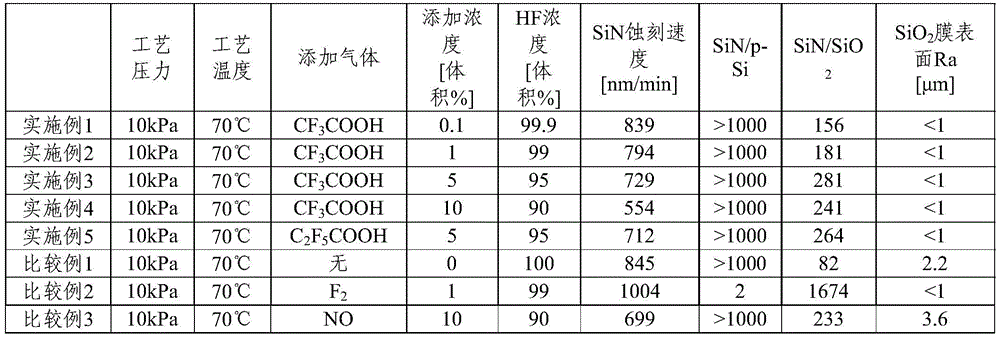
Examples 1 to 5, with p-Si and SiO2SiN can be etched selectively, and since almost no SiO is formed2The surface of the film is shaved off, so that SiO2The surface Ra of the film was 1 μm or less and was very smooth.
On the other hand, in comparative example 1, SiN, SiO were etched only with HF as in patent document 22Is also cut off, SiN/SiO2Is relatively poor. Comparative example 2 in the same manner as in patent document 3, F was added to HF2While etching SiN, p-Si by F2Etching, SiN/Si is poor. In comparative example 3, as in patent document 4, NO was added to HF to etch SiN, and SiO was present2Film damage, SiO after etching2The surface of the film is rough.
Description of the reference numerals
1: a reaction device; 2: a chamber; 3: a platform; 4: a sample; 5: an air guide port; 6: an exhaust line; 7: and a pressure gauge.
Claims (10)
1. A dry etching method is characterized in that a mixed gas containing hydrogen fluoride and fluorine-containing carboxylic acid is brought into contact with silicon nitride at a temperature of less than 100 ℃ without plasma to etch the silicon nitride.
2. The dry etching method according to claim 1, wherein the amount of the fluorine-containing carboxylic acid is 0.01 vol% or more of the total amount of the hydrogen fluoride and the fluorine-containing carboxylic acid.
3. The dry etching method according to claim 1 or 2, wherein the fluorine-containing carboxylic acid is at least one selected from the group consisting of monofluoroacetic acid, difluoroacetic acid, trifluoroacetic acid, difluoropropionic acid, pentafluoropropionic acid, and pentafluorobutyric acid.
4. A dry etching method as claimed in claim 1, wherein the mixed gas is in contact with not only the silicon nitride but also silicon oxide and polysilicon,
an etch selectivity ratio (SiN/SiO) of the silicon nitride to the silicon oxide2) And the etching selection ratio (SiN/Si) of the silicon nitride and the polycrystalline silicon is more than 100.
5. The dry etching method according to claim 1, wherein the fluorine-containing carboxylic acid is trifluoroacetic acid or pentafluoropropionic acid,
the amount of the fluorine-containing carboxylic acid is 0.1 to 30 vol% based on the total amount of the hydrogen fluoride and the fluorine-containing carboxylic acid.
6. A method for manufacturing a semiconductor device, comprising the steps of: selectively etching a silicon nitride film on a silicon substrate having a silicon oxide film, a polysilicon film and a silicon nitride film by applying the dry etching method according to any one of claims 1 to 5.
7. A dry etching gas composition comprising hydrogen fluoride and a fluorine-containing carboxylic acid.
8. The dry etching gas composition according to claim 7, comprising substantially only hydrogen fluoride and fluorine-containing carboxylic acid.
9. The dry etching gas composition according to claim 7 or 8, wherein the amount of the fluorine-containing carboxylic acid is 0.01 vol% or more of the total amount of the hydrogen fluoride and the fluorine-containing carboxylic acid.
10. An etching apparatus, comprising:
a chamber having a stage on which a silicon substrate including a silicon nitride film is placed;
a gas supply unit for supplying a dry etching gas composition containing hydrogen fluoride and a fluorocarboxylic acid to the substrate placed on the stage;
a vacuum exhaust unit for reducing the pressure in the chamber; and
a heater for heating the platform, and
the etching device etches the silicon nitride film from the substrate.
Applications Claiming Priority (3)
| Application Number | Priority Date | Filing Date | Title |
|---|---|---|---|
| JP2017-218692 | 2017-11-14 | ||
| JP2017218692 | 2017-11-14 | ||
| PCT/JP2018/039406 WO2019097964A1 (en) | 2017-11-14 | 2018-10-24 | Dry etching method |
Publications (2)
| Publication Number | Publication Date |
|---|---|
| CN111279460A true CN111279460A (en) | 2020-06-12 |
| CN111279460B CN111279460B (en) | 2023-07-18 |
Family
ID=66539502
Family Applications (1)
| Application Number | Title | Priority Date | Filing Date |
|---|---|---|---|
| CN201880068626.2A Active CN111279460B (en) | 2017-11-14 | 2018-10-24 | Dry etching method |
Country Status (6)
| Country | Link |
|---|---|
| US (2) | US11289340B2 (en) |
| JP (2) | JP7177344B2 (en) |
| KR (1) | KR102419013B1 (en) |
| CN (1) | CN111279460B (en) |
| TW (2) | TWI824482B (en) |
| WO (1) | WO2019097964A1 (en) |
Families Citing this family (2)
| Publication number | Priority date | Publication date | Assignee | Title |
|---|---|---|---|---|
| JP7372445B2 (en) * | 2021-02-19 | 2023-10-31 | 株式会社日立ハイテク | Etching method and etching equipment |
| WO2023168170A1 (en) * | 2022-03-03 | 2023-09-07 | Lam Research Corporation | Selective precision etching of semiconductor materials |
Citations (5)
| Publication number | Priority date | Publication date | Assignee | Title |
|---|---|---|---|---|
| US6140203A (en) * | 1997-10-31 | 2000-10-31 | Micron Technology, Inc. | Capacitor constructions and semiconductor processing method of forming capacitor constructions |
| US6221680B1 (en) * | 1998-07-31 | 2001-04-24 | International Business Machines Corporation | Patterned recess formation using acid diffusion |
| US20050189575A1 (en) * | 2004-02-27 | 2005-09-01 | Kevin Torek | Semiconductor fabrication that includes surface tension control |
| CN1678961A (en) * | 2002-08-22 | 2005-10-05 | 大金工业株式会社 | Removing solution |
| CN101390200A (en) * | 2006-02-23 | 2009-03-18 | 美光科技公司 | Highly selective doped oxide etchant |
Family Cites Families (17)
| Publication number | Priority date | Publication date | Assignee | Title |
|---|---|---|---|---|
| JPH06163476A (en) * | 1992-11-18 | 1994-06-10 | Sony Corp | Dry etching method |
| US5922624A (en) | 1993-05-13 | 1999-07-13 | Imec Vzw | Method for semiconductor processing using mixtures of HF and carboxylic acid |
| DE69425821T2 (en) | 1993-05-13 | 2001-04-05 | Imec Inter Uni Micro Electr | Process for etching silicon oxide layers with mixtures of HF and carboxylic acid |
| KR950033669A (en) | 1994-01-27 | 1995-12-26 | 제임스 조셉 드롱 | Nitride etching process with selectivity to oxides, silicides and silicon |
| US5626775A (en) | 1996-05-13 | 1997-05-06 | Air Products And Chemicals, Inc. | Plasma etch with trifluoroacetic acid and derivatives |
| IL119598A0 (en) | 1995-11-17 | 1997-02-18 | Air Prod & Chem | Plasma etch with trifluoroacetic acid or its derivatives |
| JPH11238725A (en) * | 1998-02-24 | 1999-08-31 | Daikin Ind Ltd | Etching composition |
| US6159859A (en) | 1998-06-09 | 2000-12-12 | Air Products And Chemicals, Inc. | Gas phase removal of SiO2 /metals from silicon |
| JP4112198B2 (en) * | 2000-09-11 | 2008-07-02 | 財団法人地球環境産業技術研究機構 | Cleaning gas and etching gas, and chamber cleaning method and etching method |
| US20080125342A1 (en) | 2006-11-07 | 2008-05-29 | Advanced Technology Materials, Inc. | Formulations for cleaning memory device structures |
| JP4833878B2 (en) | 2007-01-31 | 2011-12-07 | 東京エレクトロン株式会社 | Substrate processing method and substrate processing apparatus |
| JP2009043973A (en) | 2007-08-09 | 2009-02-26 | Tokyo Electron Ltd | Manufacturing method of semiconductor device, treatment device of semiconductor substrate, and storage medium |
| JP5101256B2 (en) | 2007-11-20 | 2012-12-19 | 東京エレクトロン株式会社 | Substrate processing method, semiconductor device manufacturing method, and computer-readable recording medium |
| JP5210191B2 (en) | 2009-02-03 | 2013-06-12 | 東京エレクトロン株式会社 | Silicon nitride film dry etching method |
| JP5655296B2 (en) * | 2009-12-01 | 2015-01-21 | セントラル硝子株式会社 | Etching gas |
| JP6073172B2 (en) | 2013-03-29 | 2017-02-01 | 岩谷産業株式会社 | Etching method |
| EP3381046B1 (en) | 2015-11-23 | 2022-12-28 | Entegris, Inc. | Process for selectively etching p-doped polysilicon relative to silicon nitride |
-
2018
- 2018-10-19 JP JP2018197338A patent/JP7177344B2/en active Active
- 2018-10-24 WO PCT/JP2018/039406 patent/WO2019097964A1/en active Application Filing
- 2018-10-24 CN CN201880068626.2A patent/CN111279460B/en active Active
- 2018-10-24 KR KR1020207015097A patent/KR102419013B1/en active IP Right Grant
- 2018-10-24 US US16/762,790 patent/US11289340B2/en active Active
- 2018-11-05 TW TW111114223A patent/TWI824482B/en active
- 2018-11-05 TW TW107139099A patent/TWI765114B/en active
-
2022
- 2022-02-22 US US17/677,367 patent/US20220172956A1/en active Pending
- 2022-11-09 JP JP2022179702A patent/JP7332961B2/en active Active
Patent Citations (5)
| Publication number | Priority date | Publication date | Assignee | Title |
|---|---|---|---|---|
| US6140203A (en) * | 1997-10-31 | 2000-10-31 | Micron Technology, Inc. | Capacitor constructions and semiconductor processing method of forming capacitor constructions |
| US6221680B1 (en) * | 1998-07-31 | 2001-04-24 | International Business Machines Corporation | Patterned recess formation using acid diffusion |
| CN1678961A (en) * | 2002-08-22 | 2005-10-05 | 大金工业株式会社 | Removing solution |
| US20050189575A1 (en) * | 2004-02-27 | 2005-09-01 | Kevin Torek | Semiconductor fabrication that includes surface tension control |
| CN101390200A (en) * | 2006-02-23 | 2009-03-18 | 美光科技公司 | Highly selective doped oxide etchant |
Also Published As
| Publication number | Publication date |
|---|---|
| US11289340B2 (en) | 2022-03-29 |
| CN111279460B (en) | 2023-07-18 |
| TWI824482B (en) | 2023-12-01 |
| JP2023001302A (en) | 2023-01-04 |
| TW202229515A (en) | 2022-08-01 |
| JP2019091890A (en) | 2019-06-13 |
| TW201923039A (en) | 2019-06-16 |
| KR20200070382A (en) | 2020-06-17 |
| JP7177344B2 (en) | 2022-11-24 |
| KR102419013B1 (en) | 2022-07-08 |
| WO2019097964A1 (en) | 2019-05-23 |
| TWI765114B (en) | 2022-05-21 |
| JP7332961B2 (en) | 2023-08-24 |
| US20220172956A1 (en) | 2022-06-02 |
| US20200365411A1 (en) | 2020-11-19 |
Similar Documents
| Publication | Publication Date | Title |
|---|---|---|
| US9330937B2 (en) | Etching of semiconductor structures that include titanium-based layers | |
| JP7332961B2 (en) | Dry etching method | |
| TWI352387B (en) | Etch methods to form anisotropic features for high | |
| US8518282B2 (en) | Method of controlling etch microloading for a tungsten-containing layer | |
| US8106485B2 (en) | Chemical oxide removal of plasma damaged SiCOH low k dielectrics | |
| JP2018529225A (en) | Nitrogen-containing compounds for etching semiconductor structures | |
| US20120289056A1 (en) | Selective silicon nitride etch | |
| KR100685735B1 (en) | Composition for removing polysilicon, method of removing polysilicon and method of manufacturing a semiconductor device using the same | |
| TW201001531A (en) | Plasma etching method | |
| CN103608898A (en) | Dielectric recovery of plasma damaged low-k films by UV-assisted photochemical deposition | |
| JP2003518738A (en) | Silicon metal mask etching method | |
| CN110047747A (en) | Engraving method and Etaching device | |
| US11827988B2 (en) | High-precision etching method | |
| JP2010098101A (en) | Method of manufacturing semiconductor device | |
| US10937659B2 (en) | Method of anisotropically etching adjacent lines with multi-color selectivity | |
| US7538037B2 (en) | Method for manufacturing semiconductor device | |
| JP2008141124A (en) | Semiconductor device, and manufacturing method thereof | |
| KR20210023906A (en) | Plasma etching method using gas molecules containing sulfur atoms | |
| JP2005268605A (en) | SELECTING ETCHANT AND ETCHING METHOD OF SiN FILM | |
| US7479461B2 (en) | Method of etching silicon anisotropically | |
| US8927431B2 (en) | High-rate chemical vapor etch of silicon substrates | |
| KR20220130597A (en) | Systems and methods for selectively etching films | |
| CN117577517A (en) | Composite substrate cleaning method | |
| CN116598198A (en) | Selective etching method | |
| JP2002009038A (en) | Treatment method of semiconductor substrate |
Legal Events
| Date | Code | Title | Description |
|---|---|---|---|
| PB01 | Publication | ||
| PB01 | Publication | ||
| SE01 | Entry into force of request for substantive examination | ||
| SE01 | Entry into force of request for substantive examination | ||
| GR01 | Patent grant | ||
| GR01 | Patent grant |