CN110537122B - Variable-focus virtual image device based on polarization conversion - Google Patents
Variable-focus virtual image device based on polarization conversion Download PDFInfo
- Publication number
- CN110537122B CN110537122B CN201880026217.6A CN201880026217A CN110537122B CN 110537122 B CN110537122 B CN 110537122B CN 201880026217 A CN201880026217 A CN 201880026217A CN 110537122 B CN110537122 B CN 110537122B
- Authority
- CN
- China
- Prior art keywords
- polarization
- light
- waveguide
- notch reflector
- lens
- Prior art date
- Legal status (The legal status is an assumption and is not a legal conclusion. Google has not performed a legal analysis and makes no representation as to the accuracy of the status listed.)
- Active
Links
- 230000010287 polarization Effects 0.000 title claims abstract description 454
- 238000006243 chemical reaction Methods 0.000 title description 26
- 239000004986 Cholesteric liquid crystals (ChLC) Substances 0.000 claims description 302
- 230000003287 optical effect Effects 0.000 claims description 275
- 239000004973 liquid crystal related substance Substances 0.000 claims description 157
- 239000011295 pitch Substances 0.000 description 69
- 239000000463 material Substances 0.000 description 35
- 238000010168 coupling process Methods 0.000 description 27
- 238000005859 coupling reaction Methods 0.000 description 27
- 230000000694 effects Effects 0.000 description 25
- 238000012545 processing Methods 0.000 description 21
- 150000001875 compounds Chemical class 0.000 description 20
- 230000001902 propagating effect Effects 0.000 description 19
- 230000008859 change Effects 0.000 description 18
- 238000009826 distribution Methods 0.000 description 18
- 238000003384 imaging method Methods 0.000 description 16
- 238000000034 method Methods 0.000 description 16
- 239000000758 substrate Substances 0.000 description 16
- 238000002347 injection Methods 0.000 description 15
- 239000007924 injection Substances 0.000 description 15
- 230000003190 augmentative effect Effects 0.000 description 14
- 239000003086 colorant Substances 0.000 description 14
- 230000008878 coupling Effects 0.000 description 13
- 230000004308 accommodation Effects 0.000 description 12
- 239000011521 glass Substances 0.000 description 10
- 230000005684 electric field Effects 0.000 description 9
- 239000000835 fiber Substances 0.000 description 9
- 238000004891 communication Methods 0.000 description 8
- 230000006870 function Effects 0.000 description 8
- 210000001747 pupil Anatomy 0.000 description 8
- 238000006116 polymerization reaction Methods 0.000 description 7
- 239000004990 Smectic liquid crystal Substances 0.000 description 6
- 230000003098 cholesteric effect Effects 0.000 description 6
- 230000007423 decrease Effects 0.000 description 6
- 238000000605 extraction Methods 0.000 description 6
- 230000005855 radiation Effects 0.000 description 6
- 230000008901 benefit Effects 0.000 description 5
- 238000000576 coating method Methods 0.000 description 5
- 238000005516 engineering process Methods 0.000 description 5
- 230000035790 physiological processes and functions Effects 0.000 description 5
- 229920000307 polymer substrate Polymers 0.000 description 5
- 101100232265 Candida albicans (strain SC5314 / ATCC MYA-2876) HWP2 gene Proteins 0.000 description 4
- 238000000429 assembly Methods 0.000 description 4
- 210000004556 brain Anatomy 0.000 description 4
- 238000005253 cladding Methods 0.000 description 4
- 239000000178 monomer Substances 0.000 description 4
- 230000008447 perception Effects 0.000 description 4
- 229920000642 polymer Polymers 0.000 description 4
- 230000008569 process Effects 0.000 description 4
- 238000001228 spectrum Methods 0.000 description 4
- 230000000007 visual effect Effects 0.000 description 4
- 230000004075 alteration Effects 0.000 description 3
- 230000003542 behavioural effect Effects 0.000 description 3
- 230000005540 biological transmission Effects 0.000 description 3
- 239000011248 coating agent Substances 0.000 description 3
- 230000003247 decreasing effect Effects 0.000 description 3
- 230000002996 emotional effect Effects 0.000 description 3
- 230000007613 environmental effect Effects 0.000 description 3
- 210000000720 eyelash Anatomy 0.000 description 3
- 239000012530 fluid Substances 0.000 description 3
- 238000002156 mixing Methods 0.000 description 3
- 239000000203 mixture Substances 0.000 description 3
- 230000002093 peripheral effect Effects 0.000 description 3
- 239000007787 solid Substances 0.000 description 3
- 230000003595 spectral effect Effects 0.000 description 3
- 230000003068 static effect Effects 0.000 description 3
- 239000000126 substance Substances 0.000 description 3
- 239000004988 Nematic liquid crystal Substances 0.000 description 2
- 239000004974 Thermotropic liquid crystal Substances 0.000 description 2
- 210000000613 ear canal Anatomy 0.000 description 2
- 230000001747 exhibiting effect Effects 0.000 description 2
- 210000000744 eyelid Anatomy 0.000 description 2
- 210000003128 head Anatomy 0.000 description 2
- 239000007788 liquid Substances 0.000 description 2
- 238000004519 manufacturing process Methods 0.000 description 2
- 238000005259 measurement Methods 0.000 description 2
- -1 nematic Substances 0.000 description 2
- 230000000737 periodic effect Effects 0.000 description 2
- 230000002829 reductive effect Effects 0.000 description 2
- 238000002310 reflectometry Methods 0.000 description 2
- 230000004044 response Effects 0.000 description 2
- 210000001525 retina Anatomy 0.000 description 2
- 238000004088 simulation Methods 0.000 description 2
- 238000007669 thermal treatment Methods 0.000 description 2
- 238000011144 upstream manufacturing Methods 0.000 description 2
- 230000016776 visual perception Effects 0.000 description 2
- 241000256837 Apidae Species 0.000 description 1
- 239000004983 Polymer Dispersed Liquid Crystal Substances 0.000 description 1
- XUIMIQQOPSSXEZ-UHFFFAOYSA-N Silicon Chemical compound [Si] XUIMIQQOPSSXEZ-UHFFFAOYSA-N 0.000 description 1
- 241000153282 Theope Species 0.000 description 1
- 238000010521 absorption reaction Methods 0.000 description 1
- 230000009471 action Effects 0.000 description 1
- 230000001174 ascending effect Effects 0.000 description 1
- 230000000712 assembly Effects 0.000 description 1
- 230000002238 attenuated effect Effects 0.000 description 1
- 230000003416 augmentation Effects 0.000 description 1
- 239000012141 concentrate Substances 0.000 description 1
- 230000001186 cumulative effect Effects 0.000 description 1
- 238000013500 data storage Methods 0.000 description 1
- 238000001514 detection method Methods 0.000 description 1
- 238000011161 development Methods 0.000 description 1
- 125000004386 diacrylate group Chemical group 0.000 description 1
- 210000004709 eyebrow Anatomy 0.000 description 1
- 230000004438 eyesight Effects 0.000 description 1
- 230000008921 facial expression Effects 0.000 description 1
- 239000010408 film Substances 0.000 description 1
- 238000010438 heat treatment Methods 0.000 description 1
- 238000005286 illumination Methods 0.000 description 1
- 230000008676 import Effects 0.000 description 1
- 238000011065 in-situ storage Methods 0.000 description 1
- 238000010348 incorporation Methods 0.000 description 1
- 238000002329 infrared spectrum Methods 0.000 description 1
- 230000002452 interceptive effect Effects 0.000 description 1
- 238000002955 isolation Methods 0.000 description 1
- 238000010030 laminating Methods 0.000 description 1
- 230000002535 lyotropic effect Effects 0.000 description 1
- 239000012528 membrane Substances 0.000 description 1
- 239000013307 optical fiber Substances 0.000 description 1
- 238000012856 packing Methods 0.000 description 1
- 230000036961 partial effect Effects 0.000 description 1
- 230000000704 physical effect Effects 0.000 description 1
- 229920000515 polycarbonate Polymers 0.000 description 1
- 239000004417 polycarbonate Substances 0.000 description 1
- 230000004478 pupil constriction Effects 0.000 description 1
- 230000010344 pupil dilation Effects 0.000 description 1
- 230000009467 reduction Effects 0.000 description 1
- 230000011514 reflex Effects 0.000 description 1
- 230000029058 respiratory gaseous exchange Effects 0.000 description 1
- 230000000717 retained effect Effects 0.000 description 1
- 230000002441 reversible effect Effects 0.000 description 1
- 229910052594 sapphire Inorganic materials 0.000 description 1
- 239000010980 sapphire Substances 0.000 description 1
- 229910052710 silicon Inorganic materials 0.000 description 1
- 239000010703 silicon Substances 0.000 description 1
- 239000011343 solid material Substances 0.000 description 1
- 125000006850 spacer group Chemical group 0.000 description 1
- 238000003860 storage Methods 0.000 description 1
- 238000006467 substitution reaction Methods 0.000 description 1
- 230000001225 therapeutic effect Effects 0.000 description 1
- 239000010409 thin film Substances 0.000 description 1
- 238000009281 ultraviolet germicidal irradiation Methods 0.000 description 1
- 230000004470 vergence movement Effects 0.000 description 1
- 238000001429 visible spectrum Methods 0.000 description 1
- 230000004304 visual acuity Effects 0.000 description 1
- 238000012800 visualization Methods 0.000 description 1
Images


Classifications
-
- G—PHYSICS
- G02—OPTICS
- G02B—OPTICAL ELEMENTS, SYSTEMS OR APPARATUS
- G02B26/00—Optical devices or arrangements for the control of light using movable or deformable optical elements
- G02B26/08—Optical devices or arrangements for the control of light using movable or deformable optical elements for controlling the direction of light
- G02B26/0816—Optical devices or arrangements for the control of light using movable or deformable optical elements for controlling the direction of light by means of one or more reflecting elements
- G02B26/0825—Optical devices or arrangements for the control of light using movable or deformable optical elements for controlling the direction of light by means of one or more reflecting elements the reflecting element being a flexible sheet or membrane, e.g. for varying the focus
-
- G—PHYSICS
- G02—OPTICS
- G02B—OPTICAL ELEMENTS, SYSTEMS OR APPARATUS
- G02B27/00—Optical systems or apparatus not provided for by any of the groups G02B1/00 - G02B26/00, G02B30/00
- G02B27/01—Head-up displays
- G02B27/017—Head mounted
- G02B27/0172—Head mounted characterised by optical features
-
- G—PHYSICS
- G02—OPTICS
- G02B—OPTICAL ELEMENTS, SYSTEMS OR APPARATUS
- G02B30/00—Optical systems or apparatus for producing three-dimensional [3D] effects, e.g. stereoscopic images
-
- G—PHYSICS
- G02—OPTICS
- G02B—OPTICAL ELEMENTS, SYSTEMS OR APPARATUS
- G02B5/00—Optical elements other than lenses
- G02B5/20—Filters
-
- G—PHYSICS
- G02—OPTICS
- G02B—OPTICAL ELEMENTS, SYSTEMS OR APPARATUS
- G02B5/00—Optical elements other than lenses
- G02B5/30—Polarising elements
-
- G—PHYSICS
- G02—OPTICS
- G02B—OPTICAL ELEMENTS, SYSTEMS OR APPARATUS
- G02B6/00—Light guides; Structural details of arrangements comprising light guides and other optical elements, e.g. couplings
- G02B6/0001—Light guides; Structural details of arrangements comprising light guides and other optical elements, e.g. couplings specially adapted for lighting devices or systems
- G02B6/0011—Light guides; Structural details of arrangements comprising light guides and other optical elements, e.g. couplings specially adapted for lighting devices or systems the light guides being planar or of plate-like form
- G02B6/0013—Means for improving the coupling-in of light from the light source into the light guide
- G02B6/0023—Means for improving the coupling-in of light from the light source into the light guide provided by one optical element, or plurality thereof, placed between the light guide and the light source, or around the light source
- G02B6/0026—Wavelength selective element, sheet or layer, e.g. filter or grating
-
- G—PHYSICS
- G02—OPTICS
- G02B—OPTICAL ELEMENTS, SYSTEMS OR APPARATUS
- G02B6/00—Light guides; Structural details of arrangements comprising light guides and other optical elements, e.g. couplings
- G02B6/0001—Light guides; Structural details of arrangements comprising light guides and other optical elements, e.g. couplings specially adapted for lighting devices or systems
- G02B6/0011—Light guides; Structural details of arrangements comprising light guides and other optical elements, e.g. couplings specially adapted for lighting devices or systems the light guides being planar or of plate-like form
- G02B6/0033—Means for improving the coupling-out of light from the light guide
- G02B6/005—Means for improving the coupling-out of light from the light guide provided by one optical element, or plurality thereof, placed on the light output side of the light guide
- G02B6/0055—Reflecting element, sheet or layer
-
- G—PHYSICS
- G02—OPTICS
- G02B—OPTICAL ELEMENTS, SYSTEMS OR APPARATUS
- G02B6/00—Light guides; Structural details of arrangements comprising light guides and other optical elements, e.g. couplings
- G02B6/0001—Light guides; Structural details of arrangements comprising light guides and other optical elements, e.g. couplings specially adapted for lighting devices or systems
- G02B6/0011—Light guides; Structural details of arrangements comprising light guides and other optical elements, e.g. couplings specially adapted for lighting devices or systems the light guides being planar or of plate-like form
- G02B6/0033—Means for improving the coupling-out of light from the light guide
- G02B6/0056—Means for improving the coupling-out of light from the light guide for producing polarisation effects, e.g. by a surface with polarizing properties or by an additional polarizing elements
-
- G—PHYSICS
- G02—OPTICS
- G02B—OPTICAL ELEMENTS, SYSTEMS OR APPARATUS
- G02B6/00—Light guides; Structural details of arrangements comprising light guides and other optical elements, e.g. couplings
- G02B6/0001—Light guides; Structural details of arrangements comprising light guides and other optical elements, e.g. couplings specially adapted for lighting devices or systems
- G02B6/0011—Light guides; Structural details of arrangements comprising light guides and other optical elements, e.g. couplings specially adapted for lighting devices or systems the light guides being planar or of plate-like form
- G02B6/0075—Arrangements of multiple light guides
- G02B6/0076—Stacked arrangements of multiple light guides of the same or different cross-sectional area
-
- G—PHYSICS
- G02—OPTICS
- G02B—OPTICAL ELEMENTS, SYSTEMS OR APPARATUS
- G02B6/00—Light guides; Structural details of arrangements comprising light guides and other optical elements, e.g. couplings
- G02B6/0001—Light guides; Structural details of arrangements comprising light guides and other optical elements, e.g. couplings specially adapted for lighting devices or systems
- G02B6/0011—Light guides; Structural details of arrangements comprising light guides and other optical elements, e.g. couplings specially adapted for lighting devices or systems the light guides being planar or of plate-like form
- G02B6/0081—Mechanical or electrical aspects of the light guide and light source in the lighting device peculiar to the adaptation to planar light guides, e.g. concerning packaging
- G02B6/0086—Positioning aspects
- G02B6/0088—Positioning aspects of the light guide or other optical sheets in the package
-
- G—PHYSICS
- G02—OPTICS
- G02F—OPTICAL DEVICES OR ARRANGEMENTS FOR THE CONTROL OF LIGHT BY MODIFICATION OF THE OPTICAL PROPERTIES OF THE MEDIA OF THE ELEMENTS INVOLVED THEREIN; NON-LINEAR OPTICS; FREQUENCY-CHANGING OF LIGHT; OPTICAL LOGIC ELEMENTS; OPTICAL ANALOGUE/DIGITAL CONVERTERS
- G02F1/00—Devices or arrangements for the control of the intensity, colour, phase, polarisation or direction of light arriving from an independent light source, e.g. switching, gating or modulating; Non-linear optics
- G02F1/01—Devices or arrangements for the control of the intensity, colour, phase, polarisation or direction of light arriving from an independent light source, e.g. switching, gating or modulating; Non-linear optics for the control of the intensity, phase, polarisation or colour
- G02F1/13—Devices or arrangements for the control of the intensity, colour, phase, polarisation or direction of light arriving from an independent light source, e.g. switching, gating or modulating; Non-linear optics for the control of the intensity, phase, polarisation or colour based on liquid crystals, e.g. single liquid crystal display cells
- G02F1/133—Constructional arrangements; Operation of liquid crystal cells; Circuit arrangements
- G02F1/13306—Circuit arrangements or driving methods for the control of single liquid crystal cells
-
- G—PHYSICS
- G02—OPTICS
- G02F—OPTICAL DEVICES OR ARRANGEMENTS FOR THE CONTROL OF LIGHT BY MODIFICATION OF THE OPTICAL PROPERTIES OF THE MEDIA OF THE ELEMENTS INVOLVED THEREIN; NON-LINEAR OPTICS; FREQUENCY-CHANGING OF LIGHT; OPTICAL LOGIC ELEMENTS; OPTICAL ANALOGUE/DIGITAL CONVERTERS
- G02F1/00—Devices or arrangements for the control of the intensity, colour, phase, polarisation or direction of light arriving from an independent light source, e.g. switching, gating or modulating; Non-linear optics
- G02F1/01—Devices or arrangements for the control of the intensity, colour, phase, polarisation or direction of light arriving from an independent light source, e.g. switching, gating or modulating; Non-linear optics for the control of the intensity, phase, polarisation or colour
- G02F1/13—Devices or arrangements for the control of the intensity, colour, phase, polarisation or direction of light arriving from an independent light source, e.g. switching, gating or modulating; Non-linear optics for the control of the intensity, phase, polarisation or colour based on liquid crystals, e.g. single liquid crystal display cells
- G02F1/137—Devices or arrangements for the control of the intensity, colour, phase, polarisation or direction of light arriving from an independent light source, e.g. switching, gating or modulating; Non-linear optics for the control of the intensity, phase, polarisation or colour based on liquid crystals, e.g. single liquid crystal display cells characterised by the electro-optical or magneto-optical effect, e.g. field-induced phase transition, orientation effect, guest-host interaction or dynamic scattering
- G02F1/13718—Devices or arrangements for the control of the intensity, colour, phase, polarisation or direction of light arriving from an independent light source, e.g. switching, gating or modulating; Non-linear optics for the control of the intensity, phase, polarisation or colour based on liquid crystals, e.g. single liquid crystal display cells characterised by the electro-optical or magneto-optical effect, e.g. field-induced phase transition, orientation effect, guest-host interaction or dynamic scattering based on a change of the texture state of a cholesteric liquid crystal
-
- G—PHYSICS
- G02—OPTICS
- G02F—OPTICAL DEVICES OR ARRANGEMENTS FOR THE CONTROL OF LIGHT BY MODIFICATION OF THE OPTICAL PROPERTIES OF THE MEDIA OF THE ELEMENTS INVOLVED THEREIN; NON-LINEAR OPTICS; FREQUENCY-CHANGING OF LIGHT; OPTICAL LOGIC ELEMENTS; OPTICAL ANALOGUE/DIGITAL CONVERTERS
- G02F1/00—Devices or arrangements for the control of the intensity, colour, phase, polarisation or direction of light arriving from an independent light source, e.g. switching, gating or modulating; Non-linear optics
- G02F1/29—Devices or arrangements for the control of the intensity, colour, phase, polarisation or direction of light arriving from an independent light source, e.g. switching, gating or modulating; Non-linear optics for the control of the position or the direction of light beams, i.e. deflection
-
- G—PHYSICS
- G02—OPTICS
- G02F—OPTICAL DEVICES OR ARRANGEMENTS FOR THE CONTROL OF LIGHT BY MODIFICATION OF THE OPTICAL PROPERTIES OF THE MEDIA OF THE ELEMENTS INVOLVED THEREIN; NON-LINEAR OPTICS; FREQUENCY-CHANGING OF LIGHT; OPTICAL LOGIC ELEMENTS; OPTICAL ANALOGUE/DIGITAL CONVERTERS
- G02F2203/00—Function characteristic
- G02F2203/07—Polarisation dependent
Landscapes
- Physics & Mathematics (AREA)
- General Physics & Mathematics (AREA)
- Optics & Photonics (AREA)
- Nonlinear Science (AREA)
- Chemical & Material Sciences (AREA)
- Crystallography & Structural Chemistry (AREA)
- Mathematical Physics (AREA)
- Liquid Crystal (AREA)
- Polarising Elements (AREA)
- Optical Filters (AREA)
- Diffracting Gratings Or Hologram Optical Elements (AREA)
- Eyeglasses (AREA)
- Optical Elements Other Than Lenses (AREA)
- Variable-Direction Aerials And Aerial Arrays (AREA)
- Aerials With Secondary Devices (AREA)
- Optical Modulation, Optical Deflection, Nonlinear Optics, Optical Demodulation, Optical Logic Elements (AREA)
- Testing, Inspecting, Measuring Of Stereoscopic Televisions And Televisions (AREA)
Abstract
An example display device includes a waveguide configured to propagate visible light under total internal reflection in a direction parallel to a major surface of the waveguide. The waveguide has an outcoupling element formed thereon, the outcoupling element being configured to outcouple a portion of the visible light in a direction perpendicular to the major surface of the waveguide. The example display device additionally includes a polarization selective notch reflector disposed on a first side of the waveguide and configured to reflect visible light having a first polarization while transmitting a portion of the visible light having a second polarization. The example display device also includes a polarization independent notch reflector disposed on a second side of the waveguide and configured to reflect visible light having the first polarization and the second polarization, wherein the polarization independent notch reflector is configured to convert a polarization of visible light reflected therefrom.
Description
Cross Reference to Related Applications
This application claims priority to U.S. provisional patent application No. 62/462,850 entitled "VARIABLE-FOCUS VIRTUAL image device" filed on 23/2/2017, which is incorporated herein by reference in its entirety. This provisional patent application includes the following sections which are incorporated by reference and form part of the present patent application:
1. part I: the specification and drawings are directed to a portion of an application entitled "DISPLAY SYSTEM WITH VARIABLE POWER REFLECTOR (display System with VARIABLE POWER Reflector)".
2. Part II: the specification and drawings are directed to a portion of an application entitled "VARIABLE-FOCUS VIRTUAL image device BASED ON POLARIZATION CONVERSION" and the like.
Sections I and II discuss variable focus or variable optical power devices and features associated with components of these devices and both sections likewise form part of the disclosure of this application. Thus, the various features, elements, structures, methods, etc. described in section I can be used, combined, incorporated, or otherwise compatible in any combination with the features, elements, structures, methods, etc. described in section II. Likewise, the various features, elements, structures, methods, etc. described in section II may be used, combined, incorporated, or otherwise compatible in any combination with the features, elements, structures, methods, etc. described in section I.
The present application also incorporates by reference the following patent applications in their entireties: U.S. application No. 14/555,585 filed on 27/11/2014; U.S. application No. 14/690,401 filed on 18/4/2015; U.S. application No. 14/212,961 filed on 3/14 of 2014; U.S. application No. 14/331,218 filed on 7/14 of 2014.
Technical Field
The present disclosure relates to display systems, and more particularly, to augmented reality display systems including diffractive devices based at least in part on polarization conversion.
Background
Modern computing and display technology has facilitated the development of systems for so-called "virtual reality" or "augmented reality" experiences, in which a digitally reproduced image, or a portion thereof, is presented to a user in a manner that appears to be, or can be perceived as, real. Virtual reality or "VR" scenes typically involve the presentation of digital or virtual image information while being opaque to other actual real-world visual inputs; augmented reality or "AR" scenes typically involve the presentation of digital or virtual image information as an augmentation to the visualization of the real world around the user. Mixed reality or "MR" scenes are "AR" type scenes and typically involve virtual objects that are integrated into and respond to the natural world. For example, in an MR scene, AR image content may be blocked by or perceived as interacting with objects in the real world.
Referring to fig. 1, an augmented reality scene 1 is shown where a user of AR technology sees a real-world park-like setting 1100 featuring people, trees, buildings in the background, and a concrete platform 1120. In addition to these items, the user of AR technology also perceives that he/she "sees" virtual content, "such as a robotic statue 1110 standing on a real world platform 1120, and a flying cartoon avatar character 1130 of an avatar that appears to be bumblebee, even though these elements 1130, 1110 do not exist in the real world. Since the human visual perception system is complex, it is challenging to generate AR technology that facilitates comfortable, natural-feeling, rich presentation of virtual image elements in addition to other virtual or real-world image elements.
The systems and methods disclosed herein address various challenges associated with AR and VR technology.
Disclosure of Invention
This application includes a discussion of systems and methods that may be used to provide variable optical power. Variable focus or variable power devices may find application in certain head mounted display devices that project images as if the images originated from different depths. By varying the optical power of the optical elements in the head mounted display device, the image presented to the wearer of the head mounted display device appears to be located at different distances from the wearer. Thus, the variable focus or variable power optical device may be modulated to cause different image content to be displayed as if the image content were located at different positions relative to the user. Some variable optical power elements include a reflector that includes a movable membrane. Other variable optical power elements include liquid crystal switchable devices that can be switched between optical power levels using switchable liquid crystal elements. Some of the variable focus devices described herein utilize polarization properties of light to facilitate switching from one focus to another.
In one aspect, a display device includes: a waveguide configured to propagate visible light under total internal reflection in a direction parallel to a major surface of the waveguide; a coupling-out element formed on the waveguide and configured to couple out a portion of the visible light in a direction perpendicular to a major surface of the waveguide. The display device further comprises: a polarization selective notch mirror disposed on a first side of the waveguide and configured to reflect visible light having a first polarization while transmitting a portion of visible light having a second polarization. The display device further includes: a polarization independent notch reflector disposed on a second side of the waveguide and configured to reflect visible light having the first and second polarizations, wherein the polarization independent notch reflector is configured to convert a polarization of the visible light reflected therefrom.
In another aspect, a display apparatus includes: a waveguide device interposed between the first switchable lens and the second switchable lens, wherein the waveguide device comprises one or more Cholesteric Liquid Crystal (CLC) layers each comprising a plurality of chiral structures, wherein each chiral structure comprises a plurality of liquid crystal molecules extending in a layer depth direction and continuously rotating in a first rotation direction, wherein an arrangement of the liquid crystal molecules of the chiral structure varies periodically in a lateral direction perpendicular to the layer depth direction such that the one or more CLC layers are configured to bragg reflect incident light. The waveguide device additionally includes one or more waveguides formed on the one or more CLC layers and configured to propagate visible light under Total Internal Reflection (TIR) in a direction parallel to a major surface of the waveguide and configured to optically couple visible light to or from the one or more CLC layers.
In another aspect, a display device configured to display an image to an eye of a user includes an optical display. The optical display has a front side and a back side, wherein the back side is closer to the user's eyes than the front side. The optical display is configured to output light having a wavelength range towards the rear side. A first notch reflector is disposed behind the optical display, the first notch reflector configured to reflect light having the wavelength range output from the optical display. A second notch reflector is disposed in front of the optical display, the second notch reflector configured to reflect light having the wavelength range. The first notch reflector is configured to substantially transmit light having a first polarization and to substantially reflect light having a second polarization different from the first polarization. The first notch reflector is configured to convert light incident behind having the second polarization into the first polarization and redirect the light back.
In another aspect, a dynamic focus display system includes a display configured to output circularly polarized light in a first circular polarization state. The display is disposed along an optical axis and has a front side and a rear side, the rear side being closer to the user's eye than the front side, the optical display being configured to output light having a wavelength range towards the rear side. A first switchable optical element is disposed along the optical axis, the first switchable optical element being configured to change a circular polarization state of light transmitted through the first switchable optical element from the first circular polarization state to a second, different circular polarization state. A first Cholesteric Liquid Crystal (CLC) lens is disposed in front of the first switchable optical element along the optical axis. A second switchable optical element is disposed in front of the first CLC lens along the optical axis, the second switchable optical element being configured to change a circular polarization state of light transmitted through the second switchable optical element from the first circular polarization state to a second, different circular polarization state. A second CLC lens is disposed in front of the second switchable optical element along the optical axis. A controller is configured to electronically switch the states of the first and second switchable optical elements to dynamically select either the first CLC lens or the second CLC lens.
In another aspect, a wearable augmented reality head-mounted display system is configured to pass light into an eye of a wearer wearing the head-mounted system from the world in front of the wearer. The wearable augmented reality head-mounted display system includes: an optical display configured to output light to form an image; one or more waveguides disposed to receive the light from the display; a frame configured to position the waveguides in front of the eye such that the one or more waveguides have an anterior side and a posterior side, the posterior side being closer to the eye than the anterior side; a Cholesteric Liquid Crystal (CLC) reflector disposed on the front side of the one or more waveguides, the CLC reflector configured to have an optical power or depth of focus that is adjustable upon application of an electrical signal; and one or more out-coupling elements disposed relative to the one or more waveguides to extract light from the one or more waveguides and guide at least a portion of the light propagating within the waveguides to the CLC reflector, the light guide being guided from the CLC reflector back through the wave and into the eye to present an image from the display into the eye of the wearer.
In another aspect, a display device includes a waveguide configured to propagate visible light under total internal reflection in a direction parallel to a major surface of the waveguide and to couple out the visible light in a direction perpendicular to the major surface. The notch reflector is configured to reflect visible light having a first polarization, wherein the notch reflector comprises one or more Cholesteric Liquid Crystal (CLC) layers, wherein each of the CLC layers comprises a plurality of chiral structures, wherein each of the chiral structures comprises a plurality of liquid crystal molecules extending in a layer depth direction and continuously rotating in a first rotation direction, wherein an arrangement of the liquid crystal molecules of the chiral structures periodically varies in a lateral direction perpendicular to the layer depth direction such that the one or more CLC layers are configured to reflect incident light.
The details of one or more implementations of the subject matter described in this specification are set forth in the accompanying drawings and the description below. Other features, aspects, and advantages will become apparent from the description, the drawings, and the claims. Neither this summary nor the following detailed description is intended to define or limit the scope of the inventive subject matter.
Drawings
Fig. 1 shows an Augmented Reality (AR) view of a user looking through an AR device.
Fig. 2 shows an example of a wearable display system.
Fig. 3 illustrates a conventional display system for simulating a three-dimensional image for a user.
FIG. 4 illustrates aspects of a method of simulating a three-dimensional image using multiple depth planes.
Fig. 5A to 5C show the relationship between the radius of curvature and the focal radius.
Fig. 6 shows an example of a waveguide stack for outputting image information to a user.
Fig. 7 shows an example of an outgoing light beam output by a waveguide.
Fig. 8 illustrates an example of a stacked waveguide assembly, wherein each depth plane includes images formed using a plurality of different component colors.
FIG. 9A illustrates a cross-sectional side view of an example of a set of stacked waveguides, each including an incoupling optical element.
Fig. 9B illustrates a perspective view of an example of the plurality of stacked waveguides of fig. 9A.
Fig. 9C illustrates a top plan view of an example of the multiple stacked waveguides of fig. 9A and 9B.
Figure 10 shows a cross-sectional side view of an example of a cholesteric liquid crystal diffraction grating (CLCG) having a plurality of uniform (uniform) chiral structures.
Fig. 11 shows a cross-sectional side view of an example of a CLCG having differently arranged chiral structures in the lateral direction.
Fig. 12 shows a cross-sectional side view of an example of a CLC layer configured to bragg reflect at an off-axis angle of incidence.
Fig. 13A shows a cross-sectional side view of an example of a CLC layer having a first pitch and configured to bragg reflect at a first off-axis angle of incidence.
Fig. 13B shows a cross-sectional side view of an example of a CLC layer having a second pitch and configured to bragg reflect at a second off-axis angle of incidence.
Fig. 13C shows a cross-sectional side view of an example of a CLCG including the CLC layers of fig. 13A and 13B having different pitches for bragg reflection at multiple off-axis incident angles and a high diffraction bandwidth in a stacked configuration.
Fig. 14 shows a cross-sectional side view of an example of a CLCG including a CLC layer with vertical regions having different pitches in the depth direction for bragg reflection at multiple off-axis angles of incidence and a high diffraction bandwidth.
Fig. 15 shows a cross-sectional side view of an example of a CLCG including a CLC layer with lateral regions having a pitch in the lateral direction for spatially varying bragg reflection.
Fig. 16 shows an example of an optical waveguide device comprising a waveguide coupled to CLCG and configured to propagate light via Total Internal Reflection (TIR).
Fig. 17A shows an example of an optical waveguide device that includes a waveguide coupled to CLCG and configured to selectively propagate light having a wavelength via Total Internal Reflection (TIR).
Fig. 17B shows an example of multiple optical waveguide devices in the same optical path, each optical waveguide device including a waveguide coupled to the CLCG and configured to selectively propagate light having a wavelength via Total Internal Reflection (TIR).
Fig. 17C shows an example of multiple optical waveguide devices in the same optical path, each optical waveguide device including a waveguide coupled to the CLCG and configured to selectively propagate light having a wavelength via Total Internal Reflection (TIR).
Fig. 18 shows an example of an optical waveguide device comprising a common waveguide coupled to a plurality of CLCGs and configured to selectively propagate light having a plurality of wavelengths via Total Internal Reflection (TIR).
Fig. 19 shows an example of an optical waveguide device comprising a waveguide coupled to CLCG and configured to propagate light via Total Internal Reflection (TIR).
Fig. 20 shows an example of an optical waveguide device comprising a waveguide coupled to a CLCG, wherein the CLCG is configured to receive incident light, and a polarization-converting reflector, wherein the waveguide is configured to bragg-reflect light from the CLCG via Total Internal Reflection (TIR).
Fig. 21A shows the optical waveguide device of fig. 20, wherein the CLCG is configured to receive linearly polarized or unpolarized incident light, and wherein the waveguide is configured to propagate light bragg reflected from the CLCG and light reflected by the reflector via Total Internal Reflection (TIR).
Fig. 21B shows the optical waveguide device of fig. 20, wherein the CLCG is configured to receive incident light polarized into orthogonal elliptically or circularly polarized light beams, and wherein the waveguide is configured to propagate light bragg reflected from the CLCG and light reflected by the reflector via Total Internal Reflection (TIR).
Fig. 22A shows an example of an optical waveguide device in the case of linear polarization or non-polarization of an incident light beam, the optical waveguide device comprising a plurality of CLC layers coupled to a common waveguide, the CLC layers comprising a first CLC layer comprising a chiral structure having a first direction of rotation and a second CLC layer comprising a chiral structure having a second direction of rotation opposite the first direction of rotation.
FIG. 22B shows the optical waveguide device of FIG. 22A in the case where the incident light is polarized into orthogonal elliptical or circularly polarized beams.
Fig. 22C shows an example of an optical waveguide device in the case of linear polarization or non-polarization of an incident light beam, the optical waveguide device comprising a plurality of CLC layers coupled to a common waveguide interposed between two CLC layers, the CLC layers comprising a first CLC layer comprising a chiral structure having a first direction of rotation and a second CLC layer comprising a chiral structure having a second direction of rotation opposite to the first direction of rotation.
Fig. 23 shows an example of an imaging system including a forward-facing camera configured to image a wearer's eye using Cholesteric Liquid Crystal (CLC) off-axis mirrors.
Fig. 24A-24F show examples of imaging systems including a forward-facing camera configured to image a wearer's eyes using CLC off-axis mirrors.
Fig. 24G and 24H illustrate an example of an imaging system including a forward-facing camera configured to image a wearer's eye using a diffractive optical element comprising a plurality of segments (segments) including one or more CLC off-axis mirrors, wherein each segment may have different optical characteristics.
Fig. 25A illustrates an example display device that includes a polarization converter and is configured to output an image to a user.
Fig. 25B illustrates an example display device that includes a polarization converter and is configured to output an image to a user.
Fig. 26A illustrates an example display device that includes a polarization converter and a switchable lens and is configured to output a virtual image to a user.
Fig. 26B illustrates an example display device that includes a polarization converter and a switchable lens and is configured to output a real image to a user.
Fig. 26C illustrates an example display device that includes a polarization converter and a switchable lens and is configured to output a virtual image to a user.
Fig. 26D illustrates an example display device that includes a polarization converter and a switchable lens and is configured to output a real image to a user.
FIG. 27A illustrates an example display device that includes a polarization converter and a Pancharatnam-Barry (PB) lens and is configured to output a virtual image to a user.
Fig. 27B illustrates an example display device including a polarization converter and a PB lens and configured to output a real image to a user.
Fig. 27C illustrates an example display device that includes a polarization converter and a PB lens and is configured to output a virtual image to a user.
Fig. 27D illustrates an example display device that includes a polarization converter and a PB lens and is configured to output a real image to a user.
Fig. 28A shows the spatial shift produced by two orthogonally polarized images formed by an example display device including a polarization converter and a PB lens.
FIG. 28B illustrates an example offset compensator including a lens pair for compensating for the spatial offset shown in FIG. 28A.
FIG. 28C illustrates the negative effect of the spatial offset shown in FIG. 28A using the embodiment of the offset compensator shown in FIG. 28B.
Fig. 29 shows an example display device including a waveguide assembly configured to asymmetrically project light and a PB lens and configured to output an image to a user.
Fig. 30 shows an example display device including a waveguide assembly with CLCG and a deformable mirror and configured to output an image to a user.
Fig. 31A-31C illustrate an exemplary reflective diffractive lens that can be implemented as part of a display device, wherein the reflective diffractive lens is formed from a patterned CLC material that functions as a reflective polarizing mirror.
Fig. 32A shows an example of chromatic aberration observed in the diffraction lens.
FIG. 32B illustrates an example reflective diffractive lens including multiple reflective diffractive lenses in a stacked configuration.
33A-33D illustrate an example reflective diffractive lens assembly and its operation for dynamically switching between different focal lengths.
Fig. 34 shows an example combination including an eyepiece configured to direct light toward the world and a waveguide assembly configured to redirect light toward the eye.
Throughout the drawings, reference numerals may be reused to indicate correspondence between the referenced elements. The drawings are provided to illustrate example embodiments described herein and are not intended to limit the scope of the present disclosure.
Detailed Description
The AR system may display virtual content to a user or viewer while still allowing the user to see the world around him. Preferably, the content is displayed on a head mounted display (e.g., as part of glasses) that projects image information to the user's eyes. In addition, the display may also transmit light from the surrounding environment to the user's eyes to allow viewing of the surrounding environment. As used herein, it should be understood that a "head mounted" display is a display that may be mounted on the head of a viewer.
Fig. 2 shows an example of a wearable display system 80. Display system 80 includes a display 62, as well as various mechanical and electronic modules and systems that support the functionality of display 62. The display 62 may be coupled to a frame 64 that is wearable by the display system user or viewer 60 and is configured to position the display 62 in front of the eyes of the user 60. In some embodiments, the display 62 may be considered glasses. In some embodiments, a speaker 66 is coupled to the frame 64 and positioned near the ear canal of the user 60 (in some embodiments, another speaker (not shown) is positioned near the other ear canal of the user to provide stereo/shapeable sound control). In some embodiments, the display system may also include one or more microphones 67 or other devices that detect sound. In some embodiments, the microphone is configured to allow a user to provide input or commands to the system 80 (e.g., selection of voice menu commands, natural language questions, etc.) and/or may allow audio communication with others (e.g., with other users of similar display systems). The microphone may also be configured as a peripheral sensor to continuously collect audio data (e.g., to passively collect from the user and/or the environment). Such audio data may include user sounds (such as heavy breathing) or environmental sounds (such as loud sounds indicating nearby events). The display system may also include peripheral sensors 30a, which may be separate from the frame 64 and attached to the body of the user 60 (e.g., on the head, torso, limbs, etc. of the user 60). As further described herein, in some embodiments, peripheral sensor 30a may be configured to acquire data characterizing a physiological state of user 60. For example, the sensors 30a may be electrodes.
With continued reference to fig. 2, the display 62 is operatively coupled to a local data processing module 70 by a communication link 68 (e.g., by a wired lead or wireless connection), and the local data processing module 70 may be mounted in various configurations, such as fixedly attached to the frame 64, fixedly attached to a helmet or hat worn by the user, embedded in headphones, or otherwise removably attached to the user 60 (e.g., in a backpack configuration, in a belt-coupled configuration). Similarly, sensor 30a may be operatively coupled to local processing and data module 70 via communication link 30b (e.g., via a wired lead or wireless connection). The local processing and data module 70 may include a hardware processor, as well as digital memory, such as non-volatile memory (e.g., flash memory or a hard drive), both of which may be used to facilitate processing, caching, and storage of data. These data include: a) data captured from sensors (which may be, for example, operatively coupled to the frame 64 or otherwise attached to the user 60), such as image capture devices (e.g., cameras), microphones, inertial measurement units, accelerometers, compasses, GPS units, radios, gyroscopes, and/or other sensors disclosed herein; and/or b) data (including data related to virtual content) acquired and/or processed using remote processing module 72 and/or remote data repository 74, which may be transferred to display 62 after such processing or retrieval. Local processing and data module 70 may be operatively coupled to remote processing module 72 and remote data repository 74 by communication links 76, 78 (such as via wired or wireless communication links) such that these remote modules 72, 74 are operatively coupled to each other and available as resources to local processing and data module 70. In some embodiments, the local processing and data module 70 may include one or more of an image capture device, a microphone, an inertial measurement unit, an accelerometer, a compass, a GPS unit, a radio, and/or a gyroscope. In some other embodiments, one or more of these sensors may be attached to the frame 64, or may be a separate structure that communicates with the local processing and data module 70 through a wired or wireless communication path.
With continued reference to fig. 2, in some embodiments, the remote processing module 72 may include one or more processors configured to analyze and process data and/or image information. In some embodiments, the remote data repository 74 may include a digital data storage facility, which may be available through the internet or other network configuration in a "cloud" resource configuration. In some embodiments, the remote data repository 74 may include one or more remote servers that provide information, such as information used to generate augmented reality content, to the local processing and data module 70 and/or the remote processing module 72. In some embodiments, all data is stored, all computations are performed in local processing and data modules, allowing for fully autonomous use from a remote module.
Perception of an image as "three-dimensional" or "3D" may be achieved by providing a slightly different presentation of the image to each eye of the viewer. Fig. 3 illustrates a conventional display system for simulating a three-dimensional image of a user. Two different images 5, 7 are output to the user, each image being for one eye 4, 6. The images 5, 7 are spaced a distance 10 from the eyes 4, 6 along an optical or z-axis parallel to the viewer's line of sight. The images 5, 7 are flat and the eyes 4, 6 can be focused on these images by assuming a single state of accommodation. Such systems rely on the human visual system to combine the images 5, 7 to provide a sense of depth and/or zoom for the combined image.
However, it should be appreciated that the human visual system is more complex and more challenging to provide a realistic perception of depth. For example, many viewers of conventional "3-D" display systems find such systems uncomfortable or unable to perceive a sense of depth at all. Without being limited by theory, it is believed that a viewer of the object may perceive the object as "three-dimensional" due to a combination of vergence and accommodation. Vergence movement of the two eyes relative to each other (e.g., rotation of the eyes such that the pupils move toward or away from each other to converge the line of sight of the eyes to fixate on an object) is closely related to the focusing (or accommodation) of the lenses and pupils of the eyes. Under normal circumstances, changing the focus of the lens of the eye or accommodating the eye to change the focus from one object to another object at a different distance will automatically result in a vergence change that matches the same distance according to a relationship known as "accommodation-vergence reflex" and pupil dilation or constriction. Also, under normal conditions, a change in vergence will trigger a change in accommodation for matching lens shape and pupil size. As noted herein, many stereoscopic or "3-D" display systems display a scene to each eye using slightly different presentations (and, therefore, slightly different images) so that the human visual system perceives a three-dimensional perspective. However, such systems are uncomfortable for many viewers, as they simply provide different presentations of the scene, except for the rest, while the eyes view all image information in a single state of accommodation and act in violation of the "accommodation-vergence reflection". A display system that provides a better match between accommodation and vergence may create a more realistic and comfortable three-dimensional image simulation, thereby helping to increase wear duration and thus compliance with diagnostic and therapeutic protocols.
FIG. 4 illustrates aspects of a method of simulating a three-dimensional image using multiple depth planes. Referring to fig. 4, objects at different distances from the eyes 4, 6 on the z-axis are accommodated by the eyes 4, 6 to bring these objects into focus (in focus). The eyes (4 and 6) assume a particular state of accommodation to bring objects at different distances along the z-axis into focus. Thus, it can be said that a particular state of accommodation is associated with a particular one of the depth planes 14, which has an associated focal length such that an object or part of an object in the particular depth plane is in focus when the eye is in the state of accommodation for that depth plane. In some embodiments, the three-dimensional imagery may be simulated by providing a different presentation of the image for each of the eyes 4, 6 and also by providing a different presentation of the image corresponding to each of the depth planes. Although shown as separate for clarity of illustration, it is understood that the fields of view of the eyes 4, 6 may overlap, for example, as the distance along the z-axis increases. Additionally, although shown as flat for ease of illustration, it is understood that the profile of the depth plane may be curved in physical space such that all features in the depth plane are in focus when the eye is in a particular state of accommodation.
The distance between an object and an eye 4 or 6 may also change the amount of divergence of light from the object seen by that eye. Fig. 5A to 5C show the relationship between the distance and the light ray divergence. The distances between the object and the eye 4 are represented in descending order by the distances R1, R2, and R3. As shown in fig. 5A to 5C, as the distance to the object decreases, the light rays become more divergent. As the distance increases, the light rays become more collimated. In other words, it can be said that the light field generated by a point (object or part of an object) has a spherical wavefront curvature that is a function of the distance of the point from the user's eye. As the distance between the object and the eye 4 decreases, the curvature increases. Thus, at different depth planes, the divergence of the light rays is also different, the divergence increasing as the distance between the depth plane and the viewer's eye 4 decreases. Although only a single eye 4 is shown for clarity in fig. 5A through 5C and other figures herein, it should be understood that the discussion regarding eye 4 may apply to both eyes 4 and 6 of the viewer.
Without being limited by theory, it is believed that the human eye can generally interpret a limited number of depth planes to provide depth perception. Thus, by providing the eye with different presentations of images corresponding to each of these limited number of depth planes, a highly reliable simulation of perceived depth may be achieved. The different presentations may be individually focused by the viewer's eyes, thereby helping to provide depth cues to the user based on eye accommodation required to bring different image features of the scene located on different depth planes into focus and/or based on observing out-of-focus of different image features on different depth planes.
Fig. 6 shows an example of a waveguide stack for outputting image information to a user. The display system 1000 includes a waveguide stack or stacked waveguide assembly 178 that may be used to provide three-dimensional perception to the eye/brain using a plurality of waveguides 1182, 1184, 1186, 1188, 1190. In some embodiments, the display system 1000 is the system 80 of fig. 2, and fig. 6 schematically illustrates portions of the system 80 in more detail. For example, waveguide assembly 1178 may be part of display 62 of fig. 2. It will be understood that in some embodiments, the display system 1000 may be considered a light field display.
With continued reference to fig. 6, the waveguide assembly 1178 may also include a plurality of features 1198, 1196, 1194, 1192 located between the waveguides. In some embodiments, the features 1198, 1196, 1194, 1192 may be one or more lenses. The waveguides 1182, 1184, 1186, 1188, 1190 and/or the plurality of lenses 1198, 1196, 1194, 1192 may be configured to transmit image information to the eye at various levels of wavefront curvature or light divergence. Each waveguide stage may be associated with a particular depth plane and may be configured to output image information corresponding to that depth plane. The image injection devices 1200, 1202, 1204, 1206, 1208 may serve as light sources for the waveguides and may be used to inject image information into the waveguides 1182, 1184, 1186, 1188, 1190, each of which may be configured to distribute incident light through each respective waveguide for output toward the eye 4, as described herein. Light exits the output surfaces 1300, 1302, 1304, 1306, 1308 of the image injection devices 1200, 1202, 1204, 1206, 1208 and is injected into the respective input surfaces 1382, 1384, 1386, 1388, 1390 of the waveguides 1182, 1184, 1186, 1188, 1190. In some embodiments, each of the input surfaces 1382, 1384, 1386, 1388, 1390 may be an edge of the respective waveguide, or may be a portion of a major surface of the respective waveguide (i.e., one of the waveguide surfaces that directly faces the world 1144 or the viewer's eye 4). In some embodiments, a single beam (e.g., a collimated beam) may be injected into each waveguide to output the entire field of view of the cloned collimated beam directed toward the eye 4 at a particular angle (and amount of divergence) corresponding to the depth plane associated with the particular waveguide. In some embodiments, one of the image injection devices 1200, 1202, 1204, 1206, 1208 may be associated with and inject light into a plurality of waveguides 1182, 1184, 1186, 1188, 1190 (e.g., three of them).
In some embodiments, the image injection devices 1200, 1202, 1204, 1206, 1208 are discrete displays, each generating image information for injection into a corresponding waveguide 1182, 1184, 1186, 1188, 1190, respectively. In some other embodiments, the image injection devices 1200, 1202, 1204, 1206, 1208 are outputs of a single multiplexed display, e.g., the multiplexed display may duct image information to each of the image injection devices 1200, 1202, 1204, 1206, 1208 via one or more optical conduits (e.g., fiber optic cables). It will be understood that the image information provided by the image injection devices 1200, 1202, 1204, 1206, 1208 may include different wavelengths or colors of light (e.g., different component colors as discussed herein).
In some embodiments, the light injected into the waveguides 1182, 1184, 1186, 1188, 1190 is provided by a light projector system 2000, the light projector system 2000 comprising a light module 2040, the light module 2040 may comprise a light emitter, such as a Light Emitting Diode (LED). Light from light module 2040 can be directed to light modulator 2030 (e.g., a spatial light modulator) via beam splitter 2050 and modified by light modulator 2030. Light modulator 2030 may be configured to vary the perceived intensity of light injected into waveguides 1182, 1184, 1186, 1188, 1190. Examples of spatial light modulators include Liquid Crystal Displays (LCDs), including Liquid Crystal On Silicon (LCOS) displays.
In some embodiments, the display system 1000 may be a scanning fiber optic display including one or more scanning fibers configured to project light in various patterns (e.g., raster scan, helical scan, lissajous pattern, etc.) into one or more waveguides 1182, 1184, 1186, 1188, 1190 and ultimately into the eye 4 of a viewer. In some embodiments, the illustrated image injection devices 1200, 1202, 1204, 1206, 1208 may schematically represent a single scanning fiber or scanning fiber bundle configured to inject light into one or more waveguides 1182, 1184, 1186, 1188, 1190. In some other embodiments, the image injection devices 1200, 1202, 1204, 1206, 1208 shown may schematically represent a plurality of scanning fibers or a plurality of scanning fiber bundles, each of which is configured to inject light into an associated one of the waveguides 1182, 1184, 1186, 1188, 1190. It should be understood that one or more optical fibers may be configured to transmit light from the optical module 2040 to one or more waveguides 1182, 1184, 1186, 1188, 1190. It should be understood that one or more intervening optical structures may be provided between the one or more scanning fibers and the one or more waveguides 1182, 1184, 1186, 1188, 1190, for example, to redirect light exiting the scanning fibers into the one or more waveguides 1182, 1184, 1186, 1188, 1190.
With continued reference to fig. 6, the waveguides 1182, 1184, 1186, 1188, 1190 may be configured to propagate light within each respective waveguide by Total Internal Reflection (TIR). The waveguides 1182, 1184, 1186, 1188, 1190 may each be planar or have another shape (e.g., curved), having top and bottom major surfaces and an edge extending between the top and bottom major surfaces. In the illustrated configuration, the waveguides 1182, 1184, 1186, 1188, 1190 may each include out-coupling optical elements 1282, 1284, 1286, 1288, 1290 configured to extract light from the waveguides by redirecting the light, propagating inside the respective waveguide, exiting the waveguide to output image information to the eye 4. The extracted light may also be referred to as outcoupled light, and the outcoupled optical element light may also be referred to as light extraction optics. At the position where the light propagating in the waveguide is irradiated to the light extraction optical element, the extracted light beam is output by the waveguide. As discussed further herein, the outcoupling optical elements 1282, 1284, 1286, 1288, 1290 may be, for example, gratings that include diffractive optical features. Although shown disposed at the bottom major surface of the waveguides 1182, 1184, 1186, 1188, 1190 for ease of description and clarity of depiction, in some embodiments, the out-coupling optical elements 1282, 1284, 1286, 1288, 1290 may be disposed at the top and/or bottom major surface, and/or may be disposed directly in the body of the waveguides 1182, 1184, 1186, 1188, 1190, as discussed further herein. In some embodiments, the out-coupling optical elements 1282, 1284, 1286, 1288, 1290 can be formed in a layer of material attached to a transparent substrate to form the waveguides 1182, 1184, 1186, 1188, 1190. In some other embodiments, the waveguides 1182, 1184, 1186, 1188, 1190 may be a single piece of material, and the out-coupling optical elements 1282, 1284, 1286, 1288, 1290 may be formed on a surface and/or in an interior of the piece of material.
With continued reference to fig. 6, as discussed herein, each waveguide 1182, 1184, 1186, 1188, 1190 is configured to output light to form an image corresponding to a particular depth plane. For example, the waveguide 1182 closest to the eye may be configured to transmit collimated light injected into such waveguide 1182 to the eye 4. The collimated light may represent an optically infinite focal plane. The next up-going waveguide 1184 may be configured to send out collimated light that passes through first lens 1192 (e.g., a negative lens) before it can reach eye 4; such a first lens 1192 may be configured to produce a slightly convex wavefront curvature such that the eye/brain interprets light from the next upstream waveguide 1184 as coming from a first focal plane that is closer inward from optical infinity toward the eye 4. Similarly, third upstream waveguide 1186 has its output light pass through first lens 1192 and second lens 1194 before reaching eye 4; the combined optical power of the first lens 1192 and the second lens 1194 (optical power) may be configured to produce another incremental wavefront curvature such that the eye/brain interprets light from the third waveguide 1186 as coming from a second focal plane that is closer inward toward the person from optical infinity than light from the next ascending waveguide 1184.
The other waveguide layers 1188, 1190 and lenses 1196, 1198 are similarly configured, with the highest waveguide 1190 in the stack sending its output through all of the lenses between it and the eye to obtain an aggregate focal power (aggregate focal power) representing the focal plane closest to the person. To compensate the lens stacks 1198, 1196, 1194, 1192 when viewing/interpreting light from the world 1144 on the other side of the stacked waveguide assembly 1178, a compensation lens layer 1180 may be provided at the top of the stack to compensate for the aggregate power of the underlying lens stacks 1198, 1196, 1194, 1192. This configuration provides as many sensing focal planes as there are waveguide/lens pairs available. Both the out-coupling optical elements of the waveguide and the focusing aspects of the lens may be static (i.e., not dynamic or electrically active). In some alternative embodiments, one or both of them may be dynamic using electroactive features.
In some embodiments, two or more of the waveguides 1182, 1184, 1186, 1188, 1190 may have the same associated depth plane. For example, multiple waveguides 1182, 1184, 1186, 1188, 1190 may be configured to output a set of images to the same depth plane, or multiple subsets of waveguides 1182, 1184, 1186, 1188, 1190 may be configured to output a set of images to the same multiple depth planes, one set of images per depth plane. This may provide the advantage of forming tiled images to provide an extended field of view at those depth planes.
With continued reference to fig. 6, the out-coupling optical elements 1282, 1284, 1286, 1288, 1290 may be configured to redirect light out of their respective waveguides and output that light with an appropriate amount of divergence or collimation for the particular depth plane associated with that waveguide. As a result, waveguides with different associated depth planes may have different configurations of out-coupling optical elements 1282, 1284, 1286, 1288, 1290 that output light with different amounts of divergence depending on the associated depth plane. In some embodiments, the light extraction optical elements 1282, 1284, 1286, 1288, 1290 may be bulk or surface features that may be configured to output light at a particular angle. For example, the light extraction optical elements 1282, 1284, 1286, 1288, 1290 may be volume holograms, surface holograms, and/or diffraction gratings. In some embodiments, the features 1198, 1196, 1194, 1192 may not be lenses; instead, they may simply be spacers (e.g., cladding and/or structures for forming air gaps).
In some embodiments, the outcoupling optical elements 1282, 1284, 1286, 1288, 1290 are diffractive features forming a diffractive pattern, or "diffractive optical element" (also referred to herein as a "DOE"). Preferably, the DOE has a sufficiently low diffraction efficiency (ratio of diffracted beam intensity to incident beam intensity) such that only a portion of the light of the beam is deflected towards the eye 4 by each intersection of the DOE, while the remainder continues to move through the waveguide via total internal reflection. The light carrying the image information is thus split into a plurality of related exit beams which exit the waveguide at a plurality of locations and as a result are exit emissions in a fairly uniform pattern towards the eye 4 for this particular collimated beam bouncing within the waveguide.
In some embodiments, one or more DOEs may be switchable between an "on" state in which they are actively diffracting and an "off" state in which they are not significantly diffracting. For example, a switchable DOE may comprise a polymer dispersed liquid crystal layer, wherein the droplets comprise a diffraction pattern in the host medium, and the refractive index of the droplets may be switched to substantially match the refractive index of the host material (in which case the pattern DOEs not significantly diffract incident light), or the droplets may be switched to a refractive index that DOEs not match the refractive index of the host medium (in which case the pattern actively diffracts incident light).
In some embodiments, a camera assembly 500 (e.g., a digital camera, including visible and infrared light cameras) may be provided to capture images of the eye 4 and/or tissue surrounding the eye 4, for example, to detect user input and/or to monitor a physiological state of the user. As used herein, a camera may be any image capture device. In some embodiments, the camera assembly 500 may include an image capture device and a light source to project light (e.g., infrared light) to the eye, which may then be reflected by the eye and detected by the image capture device. In some embodiments, the camera assembly 500 may be attached to the frame 64 (fig. 2) and may be in electrical communication with the processing modules 70 and/or 72, and the processing modules 70 and/or 72 may process image information from the camera assembly 500 to make various determinations regarding, for example, a physiological state of a user, as described herein. It should be appreciated that information about the physiological state of the user may be used to determine the behavioral or emotional state of the user. Examples of such information include a user's actions and/or a user's facial expressions. The collected environmental and/or virtual content data may then be used to triangulate a behavioral or emotional state of the user to determine a relationship between the behavioral or emotional state, the physiological state, and the environmental or virtual content data. In some embodiments, one camera assembly 500 may be used for each eye to monitor each eye separately.
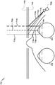
Referring now to fig. 7, an example of an outgoing beam output by a waveguide is shown. One waveguide is shown, but it is understood that other waveguides in waveguide assembly 1178 (fig. 6) may function similarly, where waveguide assembly 1178 includes a plurality of waveguides. The light 400 is injected into the waveguide 1182 at the input surface 1382 of the waveguide 1182 and propagates within the waveguide 1182 by TIR. At the point where the light 400 impinges on the DOE 282, a portion of the light exits the waveguide as an exit beam 402. The exit beam 402 is illustrated as being substantially parallel, but depending on the depth plane associated with the waveguide 1182, the exit beam 402 may also be redirected at an angle (e.g., to form a diverging exit beam) to propagate to the eye 4, as discussed herein. It will be appreciated that the substantially parallel outgoing light beams may be indicative of a waveguide having outcoupling optical elements that will couple out light to form an image that appears to be disposed on a depth plane at a large distance (e.g., optical infinity) from the eye 4. Other waveguides or other sets of outcoupling optical elements may output a more divergent exit beam pattern, which would require the eye 4 to adjust to a closer distance to focus it on the retina and would be interpreted by the brain as light from a distance closer to the eye 4 than optical infinity.
In some embodiments, a full color image may be formed at each depth plane by superimposing an image in each of the component colors (e.g., three or more component colors). Fig. 8 illustrates an example of a stacked waveguide assembly, wherein each depth plane includes images formed using a plurality of different component colors. The illustrated embodiment shows depth planes 14a-14f, but greater or lesser depths are also contemplated. Each depth plane may have three component color images associated with it: a first image of a first color G; a second image of a second color R; and a third image of a third color B. For diopters (dpt) after the letters G, R and B, different depth planes are indicated in the figure by different numbers. By way of example only, the numbers behind each of these letters represent diopters (1/m), or the inverse of the distance of the depth plane from the viewer, and each box in the figure represents a separate component color image. In some embodiments, the precise placement of the depth planes of the different component colors may vary in order to account for differences in the focus of the eye on light of different wavelengths. For example, different component color images for a given depth plane may be placed on the depth plane corresponding to different distances from the user. Such an arrangement may increase visual acuity and user comfort, and/or may reduce chromatic aberrations.
In some embodiments, each component color of light may be output by a single dedicated waveguide, and thus, each depth plane may have multiple waveguides associated therewith. In such embodiments, each box in the figure including the letter G, R or B may be understood to represent a separate waveguide, and each depth plane may provide three waveguides, with each depth plane providing three component color images. Although the waveguides associated with each depth plane are shown adjacent to each other in this figure for ease of description, it should be understood that in a physical device, the waveguides may all be arranged in a stacked fashion with one waveguide per level. In some other embodiments, multiple component colors may be output by the same waveguide, such that, for example, each depth plane may provide only a single waveguide.
With continued reference to fig. 8, in some embodiments, G is green, R is red, and B is blue. In some other embodiments, other colors associated with other wavelengths of light (including magenta and cyan) may be used in addition to or in place of one or more of red, green or blue. In some embodiments, the features 198, 196, 194, and 192 may be active or passive optical filters configured to block light from the ambient environment or selectively allow light from the ambient environment to reach the eyes of the viewer.
It should be understood that throughout this disclosure reference to light of a given color will be understood to include light of one or more wavelengths within a range of wavelengths that are perceived by a viewer as having light of that given color. For example, red light may include light at one or more wavelengths in the range of about 620-780nm, green light may include light at one or more wavelengths in the range of about 492-577nm, and blue light may include light at one or more wavelengths in the range of about 435-493 nm.
In some embodiments, the light source 2040 (fig. 6) may be configured to emit one or more wavelengths of light outside the visual perception range of the viewer, such as infrared and/or ultraviolet wavelengths of light. Furthermore, the incoupling, outcoupling and other light redirecting structures of the waveguide of the display 1000 may be configured to guide and exit this light from the display towards the eye 4 of the user, e.g. for imaging and/or user-stimulation applications.
Referring now to fig. 9A, in some embodiments, it may be desirable to redirect light impinging on the waveguide to couple the light into the waveguide. The light may be redirected and coupled into its corresponding waveguide using incoupling optics. Fig. 9A shows a cross-sectional side view of an example of a plurality or set of stacked waveguides 1200, each waveguide including an incoupling optical element. The waveguides may each be configured to output light of one or more different wavelengths, or one or more different wavelength ranges. It should be understood that the stack 1200 may correspond to the stack 1178 (fig. 6), and that the illustrated waveguides of the stack 1200 may correspond to portions of the plurality of waveguides 1182, 1184, 1186, 1188, 1190, except that light from one or more of the image injection devices 1200, 1202, 1204, 1206, 1208 is injected into the waveguides from locations where it is desired that the light be redirected to be coupled in.
The illustrated stacked waveguide set 1200 includes waveguides 1210, 1220, and 1230. Each waveguide includes an associated incoupling optical element (which may also be referred to as a light input region on the waveguide) where, for example, the incoupling optical element 1212 is disposed on a major surface (e.g., a top major surface) of the waveguide 1210, the incoupling optical element 1224 is disposed on a major surface (e.g., a top major surface) of the waveguide 1220, and the incoupling optical element 1232 is disposed on a major surface (e.g., a top major surface) of the waveguide 1230. In some embodiments, one or more of the incoupling optical elements 1212, 1222, 1232 may be disposed on the bottom major surface of the respective waveguide 1210, 1220, 1230 (particularly if one or more of the incoupling optical elements are reflective deflecting optical elements). As shown, incoupling optical elements 1212, 1222, 1232 may be disposed on the top major surface of their respective waveguides 1210, 1220, 1230 (or top of the next downstream waveguide), particularly where those incoupling optical elements are transmissive deflecting optical elements. In some embodiments, the incoupling optical elements 1212, 1222, 1232 may be disposed in the body of the respective waveguides 1210, 1220, 1230. In some embodiments, the incoupling optical elements 1212, 1222, 1232 are wavelength selective, such that they selectively redirect light of one or more wavelengths while transmitting light of other wavelengths, as discussed herein. Although shown on one side or corner of their respective waveguides 1210, 1220, 1230, it should be understood that in some embodiments the incoupling optical elements 1212, 1222, 1232 may be disposed in other regions of their respective waveguides 1210, 1220, 1230.
The incoupling optical elements 1212, 1222, 1232 may be laterally offset from one another as shown. In some embodiments, each incoupling optical element can be offset such that the incoupling optical element receives light without the light passing through another incoupling optical element. For example, as shown in fig. 6, each incoupling optical element 1212, 1222, 1232 can be configured to receive light from a different image injection device 1200, 1202, 1204, 1206, and 1208, and can be separated (e.g., laterally spaced) from other incoupling optical elements 1212, 1222, 1232 such that the incoupling optical element does not substantially receive light from other ones of the incoupling optical elements 1212, 1222, 1232.
Each waveguide further comprises an associated light distribution element, wherein, for example, light distribution element 1214 is disposed on a major surface (e.g., top major surface) of waveguide 1210, light distribution element 1224 is disposed on a major surface (e.g., top major surface) of waveguide 1220, and light distribution element 1234 is disposed on a major surface (e.g., top major surface) of waveguide 1230. In some other embodiments, the light distribution elements 1214, 1224, 1234 may be arranged on the bottom main surface of the associated waveguides 1210, 1220, 1230, respectively. In some other embodiments, light distribution elements 1214, 1224, 1234 may be arranged on the top and bottom major surfaces of the associated waveguides 1210, 1220, 1230, respectively; alternatively, the light distribution elements 1214, 1224, 1234 may be arranged on different ones of the top and bottom main surfaces in different associated waveguides 1210, 1220, 1230, respectively.
The waveguides 1210, 1220, 1230 may be spaced apart and separated by layers of, for example, gas, liquid, and/or solid material. For example, as shown, layer 1218a may separate waveguides 1210 and 1220; layer 1218b may separate waveguides 1220 and 1230. In some embodiments, layers 1218a and 1218b are formed of a low index material (i.e., a material having a lower index of refraction than the material forming one of the immediately adjacent waveguides 1210, 1220, 1230). Preferably, the refractive index of the materials forming layers 1218a, 1218b is 0.05 or more less, or 0.10 or more less, than the refractive index of the materials forming waveguides 1210, 1220, 1230. Advantageously, the lower index layers 1218a, 1218b can act as cladding layers that promote Total Internal Reflection (TIR) of light passing through the waveguides 1210, 1220, 1230 (e.g., TIR between the top and bottom major surfaces of each waveguide). In some embodiments, the layers 1218a, 1218b are formed of air. Although not shown, it is understood that the top and bottom of the illustrated waveguide set 1200 may include immediately adjacent cladding layers.
Preferably, the materials forming the waveguides 1210, 1220, 1230, and the materials forming the layers 1218a, 1218b are similar or identical, for ease of fabrication and for other considerations. In some embodiments, the material forming the waveguides 1210, 1220, 1230 may be different between one or more waveguides, and/or the material forming the layers 1218a, 1218b may be different while still maintaining the various refractive index relationships described above.
With continued reference to fig. 9A, light rays 1240, 1242, 1244 are incident on waveguide set 1200. It should be appreciated that the light rays 1240, 1242, 1244 may be injected into the waveguides 1210, 1220, 1230 by one or more image injection devices 1200, 1202, 1204, 1206, 1208 (FIG. 6).
In some embodiments, the light rays 1240, 1242, 1244 have different characteristics, e.g., different wavelengths or different wavelength ranges, which may correspond to different colors. The incoupling optical elements 1212, 122, 1232 each deflect incident light such that the light propagates through a respective one of the waveguides 1210, 1220, 1230 by TIR.
For example, the incoupling optical element 1212 may be configured to deflect light 1240 having a first wavelength or first wavelength range. Similarly, the transmitted light 1242 impinges on the incoupling optical element 1222 and is deflected by the incoupling optical element 1222, which incoupling optical element 1222 is configured to deflect light of a second wavelength or a second wavelength range. Likewise, the light 1244 is deflected by the incoupling optical elements 1232, the incoupling optical elements 1232 being configured to selectively deflect light of the third wavelength or the third wavelength range.
With continued reference to fig. 9A, the deflected light rays 1240, 1242, 1244 are deflected such that they propagate through the corresponding waveguides 1210, 1220, 1230; that is, the incoupling optical elements 1212, 1222, 1232 of each waveguide deflect light into the corresponding waveguide 1210, 1220, 1230 to couple light into the corresponding waveguide. The light rays 1240, 1242, 1244 are deflected at angles that cause the light to propagate through the respective waveguides 1210, 1220, 1230 by TIR. Light rays 1240, 1242, 1244 propagate through the respective waveguide 1210, 1220, 1230 by TIR until impinging on the waveguide's corresponding light distributing element 1214, 1224, 1234.
Referring now to fig. 9B, a perspective view of an example of the multiple stacked waveguides of fig. 9A is shown. As described above, the coupled-in light rays 1240, 1242, 1244 are deflected by the coupled-in optical elements 1212, 1222, 1232, respectively, and then propagate by TIR within the waveguides 1210, 1220, 1230, respectively. Light rays 1240, 1242, 1244 then impinge on light distribution elements 1214, 1224, 1234, respectively. Light distributing elements 1214, 1224, 1234 deflect light rays 1240, 1242, 1244 such that light rays 1240, 1242, 1244 propagate towards outcoupling optical elements 1250, 1252, 1254, respectively.
In some embodiments, the light distribution elements 1214, 1224, 1234 are Orthogonal Pupil Expanders (OPE). In some embodiments, the OPE both deflects or distributes light to the outcoupling optical elements 1250, 1252, 1254 and increases the beam or spot size of this light as it propagates towards the outcoupling optical elements. In some embodiments, for example, in embodiments where the beam size is already a desired size, the light distribution elements 1214, 1224, 1234 may be omitted and the incoupling optical elements 1212, 1222, 1232 may be configured to deflect light directly into the outcoupling optical elements 1250, 1252, 1254. For example, referring to fig. 9A, the light distribution elements 1214, 1224, 1234 may be replaced by out-coupling optical elements 1250, 1252, 1254, respectively. In some embodiments, the outcoupling optical element 1250, 1252, 1254 is an Exit Pupil (EP) or Exit Pupil Expander (EPE) that directs light into the eye 4 (fig. 7) of a viewer.
Thus, referring to fig. 9A and 9B, in some embodiments, waveguide set 1200 includes: waveguides 1210, 1220, 1230; coupling optical elements 1212, 1222, 1232; light distribution elements (e.g. OPE)1214, 1224, 1234; and out-coupling optical elements (e.g., EP)1250, 1252, 1254 for each component color. The waveguides 1210, 1220, 1230 may be stacked with an air gap/cladding between each waveguide. The incoupling optical elements 1212, 1222, 1232 redirect or deflect incident light (with different incoupling optical elements receiving light of different wavelengths) into their waveguides. The light then propagates at an angle that will result in TIR within the respective waveguide 1210, 1220, 1230. In the example shown, light 1240 (e.g., blue light) is deflected by the first incoupling optical element 1212 and then continues to bounce along the waveguide, interacting with light distribution elements (e.g., OPE)1214 and outcoupling optical elements (e.g., EP)1250, in the manner previously described. Light rays 1242 and 1244 (e.g., green and red, respectively) will be transmitted through the waveguide 1210, where the light ray 1242 impinges on the incoupling optical element 1222 and is deflected by the incoupling optical element 1222. Light ray 1242 then bounces via TIR along waveguide 1220, proceeds to its light distributing element (e.g., OPE)1224, and then proceeds to out-coupling optical element (e.g., EP) 1252. Finally, light 1244 (e.g., red light) is transmitted through the waveguide 1230 to impinge on the light incoupling elements 1232 of the waveguide 1230. The light incoupling optics 1232 deflect the light ray 1244 such that it propagates by TIR to the light distribution element (e.g. OPE)1234 and then by TIR to the outcoupling optics (e.g. EP) 1254. The out-coupling optical element 1254 then finally couples the light 1244 out to the viewer, who also receives the out-coupled light from the other waveguides 1210, 1220.
Fig. 9C illustrates a top plan view of an example of the multiple stacked waveguides of fig. 9A and 9B. As shown, the waveguides 1210, 1220, 1230 and the associated light distribution elements 1214, 1224, 1234 and the associated outcoupling optical elements 1250, 1252, 1254 of each waveguide may be vertically aligned. However, as discussed herein, the incoupling optical elements 1212, 1222, 1232 are not vertically aligned; in contrast, the incoupling optical elements are preferably non-overlapping (e.g., laterally spaced apart when viewed in plan view). As discussed further herein, this non-overlapping spatial arrangement facilitates one-to-one injection of light from different resources into different waveguides, thereby allowing a particular light source to be uniquely coupled to a particular waveguide. In some embodiments, arrangements comprising non-overlapping spatially separated incoupling optical elements may be referred to as shifted pupil systems, and the incoupling optical elements within these arrangements may correspond to sub-pupils.
Bragg reflection structure based on liquid crystal
In general, liquid crystals have physical properties intermediate between those of conventional fluids and solids. Although liquid crystals are fluid in some respects, unlike most fluids, the arrangement of molecules within a liquid crystal exhibits some structural order. Different types of liquid crystals include thermotropic liquid crystals, lyotropic liquid crystals, and polymeric liquid crystals. The thermotropic liquid crystals disclosed herein can be implemented in a variety of physical states, such as phases, including nematic, smectic, chiral nematic, or chiral smectic.
As described herein, liquid crystals in a nematic state or phase may have rod-like (calamitic) or discotic (discotic) organic molecules with a relatively small positional order and at the same time a long-range directional order with their long axes approximately parallel. Thus, organic molecules can flow freely with their centroid positions randomly distributed in the liquid while still maintaining their long range directional order. In some embodiments, the liquid crystal in the nematic phase may be uniaxial; that is, the liquid crystal has one longer preferential axis, while the other two axes are approximately equal. In other embodiments, the liquid crystal may be biaxial; that is, in addition to orienting its long axis, the liquid crystal may be oriented along the minor axis.
As described herein, a liquid crystal in a smectic state or phase may have organic molecules forming relatively well-defined layers that can slide one over the other. In some embodiments, liquid crystals in a smectic phase may be positionally ordered in one direction. In some embodiments, the long axes of the molecules may be aligned in a direction substantially perpendicular to the plane of the liquid crystal layer, while in other embodiments, the long axes of the molecules may be tilted with respect to the direction perpendicular to the plane of the layer.
In this and throughout the disclosure, nematic liquid crystals consist of rod-like molecules, where the long axes of adjacent molecules are approximately aligned with each other. To describe such an anisotropic structure, a dimensionless unit vector n called a director may be used to describe the direction of preferential alignment of liquid crystal molecules.
In this document and throughout the disclosure, the tilt or pretilt angle Φ may refer to an angle measured in a plane (e.g., x-z plane) perpendicular to a major surface (in an x-y plane) of a liquid crystal layer or a substrate and measured between an alignment direction and the major surface or a direction parallel to the major surface (e.g., x direction).
In this document and throughout the disclosure, the angle of rotation about a layer normal direction or axis perpendicular to a major surface of the liquid crystal layer is described using an azimuthal angle or angle of rotation measured in a plane parallel to the liquid crystal layer or major surface of the substrate (e.g., the x-y plane) and between an orientation direction (e.g., the direction of the elongation direction or director) and a direction parallel to the major surface (e.g., the y direction).
In this document and throughout the disclosure, when angles such as the rotation angle Φ or the pretilt angle Φ are mentioned as being substantially the same between different regions, it is understood that the average orientation angles may be, for example, within about 1%, about 5%, or about 10% of each other, although in some cases the average orientation may be greater.
In this context and throughout the description, duty cycle may for example refer to the ratio between a first lateral dimension of a first region (region) having liquid crystal molecules aligned in a first orientation direction and the grating period of the region (zone) containing the first region. Where applicable, the first region corresponds to a region in which the orientation of the liquid crystals is unchanged between different regions.
As described herein, nematic or smectic liquid crystals may also exhibit chirality. Such liquid crystals are said to be in a chiral phase or a cholesteric phase. In the chiral or cholesteric phase, the liquid crystal may exhibit a molecular twist perpendicular to the director, with the molecular axis parallel to the director. The limited twist angle between adjacent molecules is due to their asymmetric packing, which results in a longer range of chiral order.
As described herein, liquid crystals in a chiral smectic or phase may be configured such that the liquid crystal molecules have positional order in a layered structure, where the molecules are tilted at a finite angle relative to the layer normal. In addition, chirality may cause continuous azimuthal twist of liquid crystal molecules from one liquid crystal molecule in the direction of the layer normal to the next, relative to the direction perpendicular to the layer normal, resulting in helical twist of the molecular axis along the layer normal.
As described herein and throughout the disclosure, a chiral structure refers to a plurality of liquid crystal molecules in a cholesteric phase that extend, for example, in a direction perpendicular to the director (e.g., the depth of layer direction) and continuously rotate or twist in the direction of rotation (e.g., clockwise or counterclockwise). In one aspect, the director of the liquid crystal molecules in the chiral structure may be characterized as a helix with a helical pitch.
As described herein, liquid crystals in cholesteric phase that exhibit chirality can be described as having a chiral pitch or pitch (p) that corresponds to a length in the depth of layer direction that corresponds to the net rotation angle of one complete rotation of the liquid crystal molecules of the chiral structure in the first rotation direction. In other words, the pitch refers to the distance that the liquid crystal molecules undergo a full 360 ° twist. The pitch (p) may for example change upon a change in temperature or when other molecules are added to the liquid crystal host (if doped with a chiral material, an achiral liquid crystal host material may form a chiral phase), allowing the pitch (p) of a given material to be adjusted accordingly. In some liquid crystal systems, the pitch is of the same order as the wavelength of visible light. As described herein, liquid crystals exhibiting chirality may also be described as having a twist angle or rotation angle (Φ), which may refer to, for example, a relative azimuthal rotation between successive liquid crystal molecules in a layer normal direction, and as having a net twist angle or net rotation angle, which may refer to, for example, a relative azimuthal rotation between an uppermost liquid crystal molecule and a lowermost liquid crystal molecule across a specified length (e.g., a length of a chiral structure or a thickness of a liquid crystal layer).
According to various embodiments described herein, the above-described liquid crystals having various states or phases may be configured to provide various desired material properties, including, for example, birefringence, optical anisotropy, and manufacturability using thin film processes. For example, grating structures exhibiting spatially varying diffraction characteristics (e.g., gradient diffraction efficiency) can be made by varying the surface condition of the liquid crystal layer and/or mixing different liquid crystal materials.
As described herein, "polymerizable liquid crystal" may refer to a liquid crystal material that may be polymerized (e.g., in situ photopolymerized), which may also be described herein as a Reactive Mesogen (RM).
It will be appreciated that in some embodiments, the liquid crystal molecules may be polymerisable and, once polymerised, may form a large network with other liquid crystal molecules. For example, liquid crystal molecules may be linked to other liquid crystal molecules by chemical bonds or linking chemicals. Once bonded together, the liquid crystal molecules may form liquid crystal domains having substantially the same orientation and position as before being linked together. For convenience of description, the term "liquid crystal molecules" is used herein to refer to both liquid crystal molecules before polymerization and liquid crystal domains formed by these molecules after polymerization.
In accordance with certain embodiments described herein, photopolymerizable liquid crystal materials can be configured to form bragg reflective or diffractive structures, such as diffraction gratings, whose material properties (including birefringence, chirality, and ease of multiple coating) can be used to produce diffraction gratings having different material properties (e.g., birefringence, chirality, and thickness), which can result in different optical properties, such as diffraction efficiency, wavelength selectivity, and off-axis diffraction angle selectivity, to name a few.
It is to be understood that as described herein, a "transmissive" or "transparent" structure (e.g., a transparent substrate) can allow at least a portion (e.g., at least 20%, 30%, or 50%) of incident light to pass through it. Thus, in some embodiments, the transparent substrate may be a glass, sapphire, or polymer substrate. In contrast, a "reflective" structure (e.g., a reflective substrate) can reflect at least a portion (e.g., at least 20%, 30%, 50%, 70%, 90%, or more) of incident light to reflect therefrom.
The optical properties of the grating are determined by the physical structure of the grating (e.g., periodicity, depth, and duty cycle) and the material properties of the grating (e.g., refractive index, absorption, and birefringence). When liquid crystals are used, the optical properties of the grating can be controlled by controlling, for example, the molecular orientation or distribution of the liquid crystal material. For example, the grating may exhibit a graded diffraction efficiency by varying the molecular orientation or distribution of the liquid crystal material across the grating region. Such a method is described below with reference to the drawings.
Cholesteric liquid crystal diffraction grating (CLCG)
As described above with reference to fig. 6 and 7, display systems according to various embodiments described herein may include optical elements, such as incoupling optical elements, outcoupling optical elements, and light distribution elements, which may include diffraction gratings. For example, as described above with reference to fig. 7, light 400 injected into the waveguide 1182 at the input surface 1382 of the waveguide 1182 propagates within the waveguide 1182 via Total Internal Reflection (TIR). At the point where the light 400 impinges on the outcoupling optical element 1282, a portion of the light leaves the waveguide as an exit beam 402. In some implementations, any of optical elements 1182, 1282, or 1382 may be configured as diffraction gratings.
Efficient light coupling into (or out of) the waveguide 1182 can be a challenge when designing waveguide-based transparent (see-through) displays (e.g., for virtual/enhanced/hybrid display applications). For these and other applications, it is desirable for the diffraction grating to be formed from a material whose structure can be configured to optimize various optical properties, including diffraction properties. Desirable diffraction characteristics include polarization selectivity, spectral selectivity, angular selectivity, high spectral bandwidth, high diffraction efficiency, among others. To address these and other needs, in various embodiments disclosed herein, optical element 1282 is configured as a cholesteric liquid crystal diffraction grating (CLCG). As described below, the CLCG according to various embodiments may be configured to optimize polarization selectivity, bandwidth, phase profile, spatial variation of diffraction characteristics, spectral selectivity, high diffraction efficiency, and the like.
In the following, various embodiments of a CLCG configured as a reflective liquid crystal diffraction grating comprising Cholesteric Liquid Crystals (CLC) optimized for various optical properties are described. Typically, a diffraction grating has a periodic structure that splits and diffracts light into several beams that propagate in different directions. The direction of these light beams depends inter alia on the period of the periodic structure and the wavelength of the light. To optimize certain optical properties (e.g., diffraction efficiency), various material properties of the CLC may be optimized as described below for certain applications such as the out-coupling optical element 1282 (fig. 6, 7).
As described above, the liquid crystal molecules of the Cholesteric Liquid Crystal (CLC) layer in the chiral (nematic) phase or the cholesteric phase are characterized in that a plurality of liquid crystal molecules are arranged to have a continuous azimuthal twist of the director, which depends on the position of the film in the normal direction or the depth direction of the liquid crystal layer. As described herein, liquid crystal molecules arranged to have continuous azimuthal twist are collectively referred to herein as chiral structures. As described herein, the angle of azimuthal twist or rotation (Φ) is described as the angle between the directors of the liquid crystal molecules described above, relative to a direction parallel to the layer normal. The spatially varying director of the liquid crystal molecules of the chiral structure may be described as forming a helical pattern, wherein the pitch (p) is defined as the distance (e.g. in the layer normal direction of the liquid crystal layer) over which the director rotates 360 ° as described above. As described herein, the CLC layer configured as a diffraction grating has a lateral dimension by which a molecular structure of the liquid crystal is periodically repeated in a lateral direction perpendicular to the depth direction. This period in the lateral direction is called the grating period (Λ).
According to various embodiments described herein, a diffraction grating comprises a Cholesteric Liquid Crystal (CLC) layer comprising a plurality of chiral structures, wherein each chiral structure comprises a plurality of liquid crystal molecules extending at least one helical pitch in a depth direction of the layer and continuously rotating in a first rotational direction. The pitch is the length in the depth direction of the layer, which corresponds to the net rotation angle of one full rotation of the liquid crystal molecules of the chiral structure in the first rotation direction. The arrangement of the liquid crystal molecules of the chiral structure periodically changes in a lateral direction perpendicular to the layer depth direction.
FIG. 10 shows a cross-sectional side view of a Cholesteric Liquid Crystal (CLC) layer 1004 including a plurality of uniform chiral structures. CLC 1004 includes a CLC layer 1008, CLC layer 1008 including liquid crystal molecules arranged as a plurality of chiral structures 1012-1, 1012-2,. For example, the chiral structure 1012-1 includes a plurality of liquid crystal molecules 1012-1-1, 1012-1-2, a. The liquid crystal molecules of each chiral structure are continuously rotated in a first rotation direction. In the illustrated embodiment, the liquid crystal molecules are continuously rotated in a clockwise direction when viewed in the forward direction of the z-axis (e.g., the direction of the axis arrow) or the direction of propagation of the incident light beams 1016-L, 1016-R. For example, in the illustrated embodiment, the liquid crystal molecules 1012-1-1, 1012-1-2,. eta.1012-1-j of the chiral structure 1012-1 are continuously rotated, for example, by a rotation angle 1,2,. eta.j with respect to the positive x-direction. In the embodiment shown, for illustrative purposes, the plurality of liquid crystal molecules of each of the chiral structures 1012-1, 1012-2, and. Thus, the chiral structures 1012-1, 1012-2, were. However, embodiments are not so limited, and the chiral structures 1012-1, 1012-2,... 1012-i may have any number of complete rotations greater than or less than 1, have any suitable net rotation angle less than or greater than 360 °, and/or any suitable length L in the z-direction that is shorter or longer than the pitch p. For example, in various embodiments described herein, the complete number of rotations of a chiral structure can be between 1 and 3, between 2 and 4, between 3 and 5, between 4 and 6, between 5 and 7, between 6 and 8, between 7 and 9, or between 8 and 10, among other numbers of rotations.
Still referring to fig. 10, according to some embodiments, the successive rotation angles 1,2, between adjacent liquid crystal molecules in the z-direction may be the same, or according to some other embodiments, they may be different. Illustratively, in the embodiment shown, the length of the chiral structures 1012-1, 1012-2,... 1012-i is about p, and the net rotation angle is 360, such that adjacent liquid crystal molecules in the z-direction are rotated about 360/(m-1), where m is the number of liquid crystal molecules in the chiral structure. For example, to illustrate, each of the chiral structures 1012-1, 1012-2,.. 1012-i has 13 liquid crystal molecules such that adjacent liquid crystal molecules in the z-direction are rotated about 30 ° relative to each other. Of course, the chiral structures in various embodiments can have any suitable number of liquid crystal molecules.
Thus, still referring to fig. 10, adjacent chiral structures in the lateral direction (e.g., x-direction) have similarly arranged liquid crystal molecules. In the illustrated embodiment, the chiral structures 1012-1, 1012-2, the.
The CLC layer 1004 shown in fig. 10 is further described below in operation. As depicted, the CLC layer 1004 includes chiral structures 1012-1, 1012-2, a. In operation, when incident light having a combination of a left-handed circularly polarized light beam and a right-handed circularly polarized light beam is incident on surface 1004S of CLC layer 1008, light having one of the circular polarization handedness is reflected by CLC layer 1004 through bragg reflection, while light having the opposite polarization handedness is transmitted through CLC layer 1008 substantially without interference. As described herein and throughout the disclosure, handedness is defined as viewing in the direction of propagation. According to an embodiment, incident light is reflected when the polarization direction or handedness of the polarization of the light beam 1016-L, 1016-R is matched such that it has the same rotational direction as the liquid crystal molecules of the chiral structure 1012-1, 1012-2. As shown, incident on surface 1004S is light beam 1016-L having a left-hand circular polarization and light beam 1016-R having a right-hand circular polarization. In the illustrated embodiment, the liquid crystal molecules of chiral structures 1012-1, 1012-2, the. Thus, light beam 1016-R having a right-hand circular polarization is substantially reflected, while light beam 1016-L having a left-hand circular polarization is substantially transmitted through CLC layer 1004.
Without being bound by any theory, under bragg reflection conditions, the wavelength (λ) of the incident light may be proportional to the average or mean refractive index (n) and the pitch (p) of the CLC layer, and in some cases may be expressed as satisfying the following condition:

in addition, the bandwidth of the bragg reflection wavelength (Δ λ) may be proportional to the birefringence Δ n (e.g., the difference in refractive index between different light polarizations) and the pitch (p) of the CLC layer 1004, which may be expressed in some cases as satisfying the following condition:
Δλ=Δn·p [2]
in various embodiments described herein, the bandwidth Δ λ is about 60nm, about 80nm, or about 100 nm.
According to various embodiments, the peak reflected intensity in the visible wavelength range, e.g., between about 390nm and about 700nm, or in the near infrared wavelength range, e.g., between about 700nm and about 2500nm, may exceed about 60%, about 70%, about 80%, or about 90%. Additionally, according to various embodiments, the full width at half maximum (FWHM) may be less than about 100nm, less than about 70nm, less than about 50nm, or less than about 20 nm.
Fig. 11 shows a cross-sectional side view of a CLC grating (CLCG)1150 having differently arranged chiral structures in the lateral direction, e.g. chiral structures having varying twist angles in the lateral direction. Similar to the CLC layer 1004 of fig. 10, the diffraction grating 1150 includes a Cholesteric Liquid Crystal (CLC) layer 1158, the CLC layer 1158 including liquid crystal molecules arranged as a plurality of chiral structures 1162-1, 1162-2, a. For example, the chiral structure 1162-1 includes a plurality of liquid crystal molecules 1162-1-1, 1162-1-2. The liquid crystal molecules of each chiral structure are continuously rotated in the first rotation direction in a similar manner as described with reference to fig. 10. In addition, various other parameters of the chiral structure, including the length L, the number of complete rotations made by the liquid crystal molecules, and the number of liquid crystal molecules per chiral structure, are similar to the chiral structures described above with respect to FIG. 10.
However, in contrast to the embodiment shown in fig. 10, in the embodiment shown in fig. 11, the chiral structures adjacent in the lateral direction (e.g., x-direction) have liquid crystal molecules arranged differently. The chiral structures 1162-1, 1162-2,... 1162-i are configured differently in the x-direction such that liquid crystal molecules of different chiral structures at about the same depth have different rotation angles. For example, in the illustrated embodiment, the liquid crystal molecules 1162-1-1, 1162-2-1, 1162-1, the liquid crystal molecules 1162-1, 1162-2-1, the. In the illustrated embodiment, the net rotational angle of the liquid crystal molecules 1162-1-1, 1162-2-1,... 1162-i-1 that are closest to the incident surface 1158S across the lateral length Λ corresponding to the period of the diffraction grating 1150 is a rotational angle of about 180 °. In addition, the liquid crystal molecules of different chiral structures disposed at about the same depth level are rotated by about the same rotation angle with respect to the respective outermost liquid crystal molecules.
Still referring to FIG. 11, according to some embodiments, the continuous rotation angle φ of the liquid crystal molecules at the same depth level across the period Λ in the x-direction1、φ2、......φiMay be the same or, according to some other embodiments, may be different. In the illustrated embodiment, for the period Λ, when the net rotation angle is 360 ° as in the illustrated embodiment, adjacent liquid crystal molecules in the x-direction rotate by about 360 °/(m-1), where m is the periodThe number of liquid crystal molecules spanned by the period Λ in the x direction. For example, to illustrate, there are 7 liquid crystal molecules across the period Λ, such that adjacent liquid crystal molecules at the same vertical level (vertical level) in the x-direction are rotated by about 30 ° with respect to each other. Of course, the chiral structures in various embodiments can have any suitable number of liquid crystal molecules.
It should be understood that the CLC layer 1158 is shown with only one period Λ for purposes of illustration. Of course, embodiments are not so limited, and the CLC layer 1158 may have any suitable number of periods determined by the lateral dimension of the CLCG in the x-direction.
As shown by CLCG 1150, when chiral structures in a lateral direction (e.g., x-direction) are arranged differently (e.g., rotated continuously), the continuously rotated chiral structures cause a change in the relative phase of reflected light along the x-direction. This is illustrated for graph 1170, which plots 1170 rotation angle in the x-axis direction from within one period Λ The phase change phi caused by the continuously rotating chiral structure. Without being bound by any theory, the relative phase difference (Δ Φ) of the reflected light 1018 may be expressed as Δ Φ (x) ═ 2 π x/Λ, where x is the position along the lateral direction and Λ is the period. The bandwidth can be expressed as Δ λ ≈ Δ n · p.
Referring back to fig. 10-11 and equations [1] and [2], according to various embodiments, the bragg reflection wavelength may be changed by changing the pitch p of the chiral structure. In various embodiments, without being bound by any theory, the pitch p can be altered by increasing or decreasing the Helical Twisting Power (HTP), which refers to the ability of the chiral compound to induce the above-described rotation or twisting angle. The HTP can be varied by varying the amount of chiral compound relative to the amount of achiral compound. In various embodiments, by chemically and/or mechanically mixing chiral and achiral compounds (e.g., nematic compounds), the bragg reflection wavelength and color may be varied based on the relationship between the relative proportions of chiral compounds and the pitch. In various embodiments disclosed herein, the weight ratio of the amount of chiral compound to the amount of achiral compound can be about 20:1, 10:1, 5:1, 4:1, 3:1, 2:1, 1:2, 1:3, 1:4, 1:5, 1:10, or about 1: 20.
In the description above with respect to fig. 10 and 11, incident light beams 1016-L, 1016-R are shown to propagate in a direction parallel to the layer normal, e.g., in the z-direction. However, for various applications, for example, as described above with respect to fig. 6 and 7, light propagating within the waveguide 1182 (e.g., propagating via Total Internal Reflection (TIR)) impinges at an off-axis angle on the out-coupling optical elements 1282, 1284, 1286, 1288, 1290 (e.g., diffraction gratings). As described below, the diffraction gratings described herein may be configured to maximize the bandwidth and diffraction efficiency of such configurations.
In the above description with respect to fig. 10 and 11, the liquid crystal molecules are shown as not being pretilted. However, embodiments are not so limited, and the liquid crystal molecules may have a pretilt Φ between about +/-60 degrees and about +/-90 degrees, or between about +/-65 degrees and about +/-85 degrees, such as about +/-75 degrees, according to some embodiments, with respect to a direction parallel to the major surfaces of the CLCG (e.g., with respect to the x-y plane); between about +/-35 degrees and about +/-65 degrees or between about +/-40 degrees and about +/-60 degrees, such as about +/-50 degrees; between about +/-10 degrees and about +/-40 degrees or between about +/-15 degrees and about +/-35 degrees, such as about +/-25 degrees. According to some other embodiments, the pretilt angle Φ may be between about ± 15 degrees or between about ± 10 degrees or between about ± 5 degrees, e.g., 0 degrees.
CLCG configured for high bandwidth reflection at off-axis incidence angles
Fig. 12 shows a cross-sectional side view of a CLC layer 1158 configured for high bandwidth reflection at an off-axis angle of incidence. As described herein, an off-axis angle of incidence refers to the angle of incidence θ of the incident light beam 1216 relative to the layer normal direction (e.g., the z-direction in FIG. 12)incWhich has a non-zero value, resulting in a bragg reflected beam 1220 at the reflection angle theta. In some cases, the reflection angle can be varied to some extent by varying λ/Λ. Without being bound by any theory, in some cases, off-axis reflections can be described based on the following relationship:
n·sin(θ)=λ/Λ+sin(θinc) [3]
where θ inc is the angle of incidence with respect to the layer normal direction, θ is the angle of reflection with respect to the layer normal direction, and n is the reflectivity of the medium in which the reflected beam propagates. When the CLC layer 1158 is illuminated with the incident light beam 1216 at an off-axis angle, the reflection spectrum may shift toward shorter wavelengths. According to various embodiments disclosed herein, the ratio λ/Λ may have a value between 0.5 and 0.8, between 0.6 and 0.9, between 0.7 and 1.0, between 0.8 and 1.1, between 0.9 and 1.2, between 1.0 and 1.6, between 1.1 and 1.5, or between 1.2 and 1.4.
Without being bound by any theory, the off-axis angle at which the CLC layer 1158 is configured to bragg reflect with high efficiency may also depend on the pitch p of the chiral structure.
Fig. 13A and 13B show cross-sectional side views of a CLC layer configured to reflect at an off-axis incident angle. Referring to fig. 13A, a first Cholesteric Liquid Crystal (CLC) layer 1358A includes a first plurality of chiral structures having a first pitch (p 1). The first CLC layer 1358A has a first pitch p1 such that when the first incident light beam 1316A is at a first off-axis angle θinc,1When directed to the incident surface of the CLC layer 1358A, the bragg reflection is maximized, which results in a first reflected light beam 1320A at a first reflection angle θ 1. As shown, the CLC layer 1358A is also configured to have a first range of off-axis incident angles 1324A in which a relatively high diffraction efficiency may be obtained. The first range 1324A may correspond to an off-axis range of incident angles outside of which the intensity of the first reflected light beam 1320A drops off by more than, for example, 1/e. For example, the first range 1324A may have the following values: thetainc,1±3°、θinc,1±5°、θinc,1±7°、θinc,110 DEG or thetainc,1±20°。
Referring to fig. 13B, a second Cholesteric Liquid Crystal (CLC) layer 1358B, different from the first CLC layer 1358A, includes a second plurality of chiral structures having a second pitch (p) different from the first pitch p1 of the first CLC layer 1358A of fig. 13A2)。
As shown, the second CLC layer 1358B is configured such thatWhen the second incident beam 1316B is at a different angle than the first off-axis angle thetainc,1Second off-axis angle theta ofinc,2Is directed to the incident surface of the CLC layer 1358B, is generated to have an angle of reflection θ different from the first1Second reflection angle theta2The second reflected light beam 1320B. As shown, the CLC layer 1358B is also configured to have a second range 1324B of off-axis angles, which is similar to the first range 1324A described above with respect to fig. 13A.
Fig. 13C shows a cross-sectional side view of a CLCG 1358, the CLCG 1358 including a plurality of CLC layers having different pitches in a stacked configuration for bragg reflection at off-axis incident angles and a high diffraction bandwidth. The CLCG 1358 includes CLC layers 1358A, 1358B described above with respect to fig. 13A and 13B, respectively, with the CLC layers 1358A, 1358B being formed on top of one another, e.g., in a stacked configuration and/or in contact with one another. Various parameters of the multiple CLC layers 1358A, 1358B comprising different pitches may be refined or optimized such that the CLCG 1358 is configured to efficiently reflect at multiple off-axis angles of incidence and high diffraction efficiency over a wider range of off-axis angles than would be obtained using only one CLC. For example, in the illustrated embodiment, p may be selected1And p2Such that the resulting first and second ranges 1324A and 1324B at least partially overlap to provide high diffraction efficiency over a continuous range of wavelengths including the first and second ranges 1324A and 1324B. However, in other embodiments, p may be substituted1And p2Chosen so that the first and second ranges 1324A and 1324B do not overlap.
In operation, the first and second CLC layers 1358A, 1358B are formed on top of each other such that when the first and second incident light beams 1316A, 1316B are at first and second off-axis angles θinc1、θinc2When directed to an incident surface of the first CLC layer 1358A, a first incident light beam 1316A is substantially reflected by the first CLC layer 1358A at a first reflection angle θ1Reflects and the second incident light beam 1358B is substantially transmitted through the first CLC layer 1358A towards an incident surface of the second CLC layer 1358B and is substantially reflected by the second CLC layer 1358B at a second reflection angle θ2And (4) reflecting. It should be understood, although for clarity reasons the description is providedSee not shown, but the concepts described above can be extended to any suitable number of CLC layers.
As described herein and throughout the specification, a light beam "substantially transmitted" through a layer may refer to light that is retained by at least 20%, 30%, 50%, 70%, or 90% of the incident light intensity as the light exits the layer. Similarly, a light beam that is "substantially reflected" by a layer may refer to light that at least 20%, 30%, 50%, 70%, or 90% of the incident light intensity remains in the reflected light.
Still referring to fig. 13C, in various embodiments, the liquid crystal molecules of the first and second CLC layers 1358A, 1358B may include different amounts of the same chiral compound, such that the CLC layers 1358A, 1358B have different Helical Twisting Powers (HTPs), as described above. For example, second CLC layer 1358B may have a higher amount of the same chiral compound than first CLC layer 1358A. In some embodiments, the pitch p may be inversely proportional to the fraction (fraction) of chiral compound relative to the bulk liquid crystal compound comprising chiral and achiral compounds. However, the embodiment is not limited thereto, and the first and second CLC layers 1358A, 1358B may have different chiral compounds.
Additionally, in various embodiments, the liquid crystal molecules of the first and second CLC layers 1358A, 1358B may include the same or different chiral compounds, such that the CLC layers 1358A, 1358B have different ratios λ/Λ, respectively1And lambda/lambda2Such that the CLC layers 1358A, 1358B may be configured to achieve different angles of incidence θinc1、θinc2High diffraction efficiency, e.g. according to equation [3 ]]。
Still referring to fig. 13C, according to some embodiments, first and second CLC layers 1358A, 1358B may be fabricated directly on top of each other. For example, a first CLC layer 1358A may be deposited on an alignment layer (alignment layer) that provides an alignment condition for first CLC layer 1358A, and subsequently, a second CLC layer 1358B may be deposited on first CLC layer 1358B. Under these manufacturing conditions, the surface of first CLC layer 1358A may provide a directional condition for second CLC layer 1358B. In some other embodiments, each of the CLC layers 1358A, 1358B may be fabricated with a separate orientation layer. For example, a first CLC layer 1358A may be formed on the first orientation layer, a second orientation layer may be formed on the first CLC layer 1358A, and a second CLC layer 1358B may be formed on the second orientation layer. According to some embodiments, an isolation layer, such as a thin oxide layer, may be formed on first CLC layer 1358A prior to forming a second orientation layer and/or second CLC layer 1358B. In other embodiments, the two CLC layers 1358A, 1358B may be fabricated separately on different substrates and then stacked. In various embodiments, an intermediate layer may be formed between the two CLC layers 1358A, 1358B, for example to enhance adhesion.
The concepts described above with respect to a CLCG having multiple CLC layers optimized to achieve optimal diffraction efficiencies at different off-axis angles may be extended to other alternative embodiments. In particular, in some embodiments, instead of forming multiple layers, a single CLC layer may be configured to have different regions optimized to achieve optimal diffraction efficiency at different off-axis angles.
Fig. 14 shows a cross-sectional side view of a CLCG 1400 including a single CLC layer 1404 having vertical regions with different pitches in the depth direction for bragg reflection at different off-axis angles of incidence at the vertical regions and a high diffraction bandwidth. The CLC layer 1404 has a plurality of vertical regions having different parameters, e.g., different pitches, optimized such that high diffraction efficiency can be obtained over a wider range of off-axis angles than can be obtained using only one CLC layer (which has a uniform spacing in the depth direction). In the illustrated embodiment, the single CLC layer 1404 includes a plurality of vertical regions 1404A, 1404B, 1404C, and 1404D, which may each have a different pitch p1、p2、p3And p4. Similar to that described above with respect to FIG. 13C, the pitch p may be selected1、p2、p3And p4Such that the plurality of vertical regions 1404A, 1404B, 1404C, and 1404D are respectively configured to achieve the incident angle θincA、θincB、θincCAnd thetaincDOptimum diffraction efficiency, which results in corresponding reflection angles theta at different vertical depths, respectivelyA、θB、θCAnd thetaDTo reflect the light beam. Furthermore, as described above with respect to fig. 13C, the CLC layer 1404 is also configured to have a corresponding off-axis angular range within which relatively high diffraction efficiencies can be obtained. Of course, although four vertical regions are shown for clarity, any suitable number of regions may be included in the CLC layer 1404. Furthermore, the different variations described above with respect to CLCG 1358 having multiple CLC layers of fig. 13C may be applied to CLCG 1400.
In the embodiment shown in fig. 14, the pitch p1、p2、p3And p4Decreases with increasing depth from the incident surface 1404S, so that a gradually decreasing pitch gradient is generated in the depth direction (negative z direction). When the rate of decrease of pitch as a function of layer depth in the z-direction is uniform across the entire thickness of the CLC layer 1404, a graph 1408 representing a linear relationship between depth and pitch may be obtained. However, the embodiments are not limited thereto. For example, according to some other embodiments, the pitch p1、p2、p3And p4May increase or decrease at any depth and may change at different rates depending on the depth of layer.
The CLC layer 1404 having a pitch gradient can be fabricated by changing (e.g., increasing or decreasing) the helical twisting force (HTP) of the liquid crystal molecules at different depths of the CLC layer. By varying the relative amounts of the chiral compounds, the HTP can in turn be varied spatially. In various embodiments, by chemically and/or mechanically mixing chiral and achiral compounds (e.g., nematic compounds) at different vertical depths, the pitches of the vertical regions 1404A, 1404B, 1404C, and 1404D can be configured to achieve different angles of incidence θ, respectively, based on the inverse relationship between the relative fractions of the chiral compounds and the pitchesincA、θincB、θincCAnd thetaincDThe best diffraction efficiency. For example, a mixture of different chemical components (e.g., chiral bisacrylate monomers and nematic/achiral monoacrylate monomers) that undergo a polymerization process under UV radiation at different reaction rates can be used. Additionally or alternatively, by changing the CLCThe irradiation conditions of the UV radiation (including exposure intensity and/or exposure time) at different depths of the layer may cause the HTP to vary spatially. The HTP can also be varied spatially by varying the pre/post treatment of the UV polymerization process, including thermal treatment before, after and/or during UV irradiation. For example, when a UV absorbing dye is added to the mixture, an intensity gradient of UV light at different depths of the CLC layer may be generated. For example, due to the UV intensity gradient, polymerization near the surface can proceed at a faster rate than the bottom region of the CLC layer. For example, when the cholesteric component is a diacrylate, the likelihood of incorporation into the resulting polymer may be much higher, e.g., twice as high as the likelihood of a nematic monoacrylate being incorporated into the polymer. In some cases, if the overall polymerization rate is controlled, the consumption of the chiral bisacrylate near the surface region of the CLC layer results in a bisacrylate concentration gradient in the depth direction of the CLC layer. This in turn causes the bisacrylate to begin to diffuse towards the surface area of the CLC layer. The result after complete photopolymerisation may be that the surface region of the CLC layer contains more chiral material and therefore has a shorter pitch than the bottom region of the CLC layer (which contains a relatively large amount of achiral compound). In certain other cases, a heat treatment before/after or during UV radiation may be added to the polymerization process to control the pitch gradient. Thus, by controlling the ratio between two different liquid crystal monomers and/or the dose of UV radiation at different depths with or without a thermal treatment, a pitch gradient can be achieved in the depth direction of the CLC layer.
For some applications it may be desirable to have a diffraction grating with certain optical properties (such as off-angle diffraction efficiency, refractive index, wavelength selectivity, polarization selectivity, and phase selectivity, among other parameters) that vary along a lateral direction that is orthogonal to the layer normal direction. For example, when a grating is stacked with a waveguide (e.g., as described above with respect to fig. 6 and 7), lateral variation is desired such that light propagates in a lateral direction. However, in this configuration, the intensity of the light may be attenuated as it propagates within the waveguide (e.g., 1182 in fig. 7). For example, such a configuration may also be desirable to intentionally skew (skew) the light intensity across the grating (e.g., 1282 in fig. 7) to accommodate spatial and/or angular variations in sensing efficiency associated with the human eye to maximize the user experience. Therefore, there is a need for optical elements having spatially varying optical properties, such as diffraction gratings.
Fig. 15 shows a cross-sectional side view of a CLCG including a CLC layer with lateral regions having different pitches in the lateral direction for spatially varying bragg reflection. The CLC layer 1424 has a plurality of lateral regions with different liquid crystal material parameters (e.g., pitch) so that laterally varying characteristics, such as laterally varying off-axis incident angles for bragg reflection, can be obtained. In the illustrated embodiment, the CLC layer 1424 includes a plurality of lateral regions 1424A, 1424B, and 1424C, each having a period Λ and having a respective pitch p1、p2And p3. The pitch p of the thread can be selected1、p2And p3Such that the multiple vertical regions 1424A, 1424B, and 1404C are configured for different off-axis angles of incidence θincA、θincBAnd thetaincCOptimum diffraction efficiency of (A), which respectively result in corresponding reflection angles thetaA、θBAnd thetaCIs reflected light. Furthermore, as described above with respect to fig. 13C, the different lateral regions of CLC layer 1424 are also configured to have similar respective off-axis angular ranges in which relatively high diffraction efficiencies may be obtained. Of course, although three vertical regions are shown for clarity, any suitable number of regions may be included in the CLC layer 1424.
In the embodiment shown in fig. 15, the pitch p1、p2And p3May vary monotonically in the lateral direction, thereby creating a gradient in pitch. When the rate of change of pitch in the x-direction is uniform across the width or length of the CLC layer 1424, a linear relationship between the length or width and pitch can be obtained, as shown in the graph 1428 representing a. However, the embodiments are not limited thereto. For example, according to various other embodiments, the pitch p1、p2And p3May increase or decrease at any lateral position, and may be alongThe length or width changes at different rates in the x-direction.
According to various embodiments, a CLC layer may be fabricated with a diffractive property that varies laterally by, for example, spatially varying orientation properties or other material properties of the liquid crystal molecules. For example, in a similar manner as described above with respect to fig. 14, a transverse pitch gradient along the transverse dimension may be achieved, for example by controlling the ratio between two different liquid crystal monomers and/or the UV radiation dose in different transverse regions.
Waveguide coupling with CLCG to achieve wavelength selective optical coupling
As described above, for various applications including the coupling in and out of light, the waveguide arrangement may be configured to propagate light via Total Internal Reflection (TIR). Fig. 16 shows an example of an optical waveguide device 1600 that includes a waveguide 1604 coupled to CLCG 1150. The CLCG 1150 includes liquid crystal molecules arranged as a plurality of chiral structures in a manner similar to the chiral structures 1162-1, 1162-2. Waveguide 1604 is disposed over CLCG 1150 and optically coupled to CLCG 1150. When the elliptically/circularly polarized incident light 1016-R/L has a polarization handedness that matches the direction of rotation of the liquid crystal molecules of the chiral structure, the incident light 1016-R/L is Bragg reflected by the CLCG 1150 and coupled into the waveguide 1604 at an angle such that the coupled light propagates in the lateral direction (e.g., the x-direction) via Total Internal Reflection (TIR). Without being bound by any theory, when the diffraction angle θ is greater than the critical angle θ of the waveguideCThe TIR condition can be satisfied. In some cases, the TIR condition may be expressed as:
sin(θC)=1/nt [4]
wherein n istIs the refractive index of the waveguide 1604. According to various embodiments, ntMay be between about 1 and about 2, between about 1.4 and about 1.8, or between about 1.5 and about 1.7. For example, the waveguide may comprise a polymer, such as polycarbonate or glass.
FIG. 17A shows a first optical waveguide device 1700A that includes a first waveguide 1704A, the first waveguide 1704A being coupledIs incorporated into the first CLCG 1750A and is configured when theta>θc3Propagating via Total Internal Reflection (TIR) having a third wavelength λ3Of (2) is detected. The first CLCG 1750A has a first period Λ1And a first pitch p1. According to some embodiments, the first waveguide apparatus 1700A may be configured to propagate light within the visible spectrum (e.g., wavelengths between about 400nm and 700 nm) via TIR. According to some other embodiments, the first waveguide apparatus 1700A may be configured to propagate light via TIR in the infrared spectrum (e.g., the near infrared portion of the spectrum having wavelengths between about 700nm and 1400 nm). As described above with respect to FIGS. 10 and 11, Bragg reflection occurs from equation [1] above]At the wavelength indicated, and by equation [2] above]Within the bandwidth of the indicated wavelength Δ λ. For example, the first CLCG 1750A may be designed to couple the third incident light 1736 via TIR, the third incident light 1736 having one of blue (e.g., about 450nm), green (e.g., about 550nm), red (e.g., about 650nm), or a third wavelength λ in the infrared3. As shown, when Δ λ is about 60nm, about 80nm, or about 100nm, as described above, there are first and second wavelengths λ1、λ2Is substantially transmitted because equation [4 ] is not satisfied for these reasons]While colors not coupled into the first waveguide 1704 do not satisfy equation [1]]。
Fig. 17B shows a second optical waveguide device 1700B in combination with the first optical waveguide device 1700A shown above with respect to fig. 17A. The optical waveguide device 1700B is disposed behind the optical waveguide device 1700A in the optical path and includes a second waveguide 1704B, the second waveguide 1704B being coupled to a second CLCG 1750B and configured when θ>θc2While propagating via Total Internal Reflection (TIR) having a second wavelength λ 21726, respectively. The second CLCG 1750B has a second periodicity Λ2And a second pitch p2. As described above with respect to fig. 17A, having first and second wavelengths λ1、λ2Substantially transmits through the first optical waveguide device 1700A first and second light 1716 and 1726. Of the transmitted first and second light 1716 and 1726, second CLCG 1750B may be designed as θ> θc2While coupling via TIRA second incident light 1726, the second incident light 1726 having a second wavelength λ that is transmissive in one of blue (e.g., about 450nm), green (e.g., about 550nm), red (e.g., about 650nm), or infrared2. Thus, as shown, when Δ λ is about 60nm, about 80nm, or about 100nm, as described above, there is a first wavelength λ1Substantially further transmitted through the second waveguide arrangement 1700B.
FIG. 17C shows a third optical waveguide device 1700C in combination with the first and second optical waveguide devices 1700A and 1700B shown above with respect to FIG. 17B. A third optical waveguide device 1700C is disposed in the optical path after the first and second optical waveguide devices 1700A and 1700B and includes a third waveguide 1704C that is coupled to a third CLCG 1750C and configured when θ>θc1Propagating via Total Internal Reflection (TIR) having a first wavelength λ 21716. Third CLCG 1750C having third period Λ3And a third pitch p3. As described above with respect to fig. 17B, having a first wavelength λ1Substantially transmitted through the first and second waveguide arrangements 1700A and 1700B. The third CLCG 1750C may be designed when theta is larger>θc1The first incident light 1716 is coupled via TIR, the first incident light 1716 having a first wavelength λ transmitted in one of blue (e.g., about 450nm), green (e.g., about 550nm), red (e.g., about 650nm), or infrared1. Thus, as shown, when Δ λ is about 60nm, about 80nm, or about 100nm, as described above, because equation [4 ] is satisfied]Having a first wavelength λ1Is substantially coupled into the third waveguide 1704C.
Thus, as described above with respect to fig. 17A-17C, by placing one or more of the first, second, and third optical waveguide devices 1700A, 1700B, and 1700C in the same optical path, with different wavelengths λ1、λ2And λ3May be coupled to propagate via TIR in one of the first, second, and third waveguides 1704A, 1704B, and 1704C, respectively. Although in each of fig. 17A to 17C, the first to third lightsEach of the optical waveguide devices 1704A, 1704B, and 1704C has dedicated first to third waveguides 1704A, 1704B, and 1704C, respectively, and dedicated first to third CLCGs 1750A, 1750B, and 1750C, respectively, but the embodiment is not limited thereto. For example, a single waveguide may couple bragg reflected light from a stack of multiple CLCGs via TIR, as shown below with respect to fig. 18. Further, any suitable number of optical waveguide devices greater than three (or less than three) may be combined for further selective coupling by bragg reflection.
Fig. 18 shows an optical waveguide device 1800 that includes a common waveguide 1704 coupled to a plurality of CLCGs 1750. The plurality of CLCGs 1750 are configured as a stack including first through third CLCGs 1750A through 1750C and configured to propagate via Total Internal Reflection (TIR) having third, second, and first wavelengths λ, respectively3、λ2And λ 11736, 1726 and 1716. When one or more of the third, second, and first lights 1736, 1726, and 1716, respectively, satisfy the condition θ>θc3、θ>θc2And theta>θc1TIR occurs in a similar manner as described above with respect to fig. 17A-17C. Also in a similar manner, the first, second, and third CLCGs 1750A, 1750B, and 1750C are configured when θ is>θc3、θ>θc2And theta>θc1Selectively bragg reflecting the third, second and first light 1736, 1726 and 1716, respectively. Of course, any suitable number of CLCGs less than or greater than three (or less than three) may be stacked for further selective coupling by bragg reflection. Thus, a more compact waveguide arrangement 1800 may be obtained by employing a common waveguide 1704 as compared to the embodiments described above with respect to fig. 17B and 17C. Also, instead of three different CLCG layers (as shown in fig. 18), the stack of CLCG layers may be arranged with a pitch gradient (including from p1To p3Range(s) of a single (or multiple) layers.
As described above with respect to fig. 17A to 18, the first to third CLCGs 1750, 1750B, 1750C have the first to third periods Λ, respectively1、Λ2And Λ3And first toThird pitch p1、p2And p3. In various embodiments, each CLCG may be configured such that the wavelength/period ratio λ/Λ is between about 0.3 and 2.3, between about 0.8 and 1.8, or between about 1.1 and about 1.5, such as about 1.3. Alternatively, the period (Λ) may be configured to be smaller by an amplitude between about 1nm and 250nm, between about 50nm and 200nm, or between about 80nm and 170nm, as compared to a corresponding wavelength (λ) at which the CLCG is configured for bragg reflection. For example, when λ1、λ2And λ3In the visible range (e.g., about 620nm to about 780nm, e.g., about 650nm (red); about 492nm to about 577nm, e.g., 550nm (green), and about 435nm to about 493nm, e.g., about 450nm (blue), respectively), the corresponding period Λ is1、Λ2And Λ3May be about 450nm to about 550nm, such as about 500nm, respectively; about 373nm to about 473nm, for example about 423 nm; and about 296nm to about 396nm, e.g., about 346 nm. Or, when λ1、λ2And λ3In the infrared range (e.g., in the near infrared range between about 750nm and about 1400nm, such as about 850nm), the corresponding period Λ1、Λ2And Λ3And may be about 975nm to about 1820nm, such as about 1105 nm. Additionally, in various embodiments, each CLCG may be configured such that the wavelength/pitch ratio λ/p is between about 0.6 and 2.6, between about 1.1 and 2.1, or between about 1.4 and about 1.8, such as about 1.6. Alternatively, the pitch (p) may be configured to be smaller by an amplitude between about 50nm and 350nm, between about 100nm and 300nm, or between about 140nm and 280nm, as compared to the corresponding wavelength (λ) at which the CLCG is configured for bragg reflection. For example, when λ1、λ2And λ3From about 620nm to about 780nm, for example about 650nm (red), respectively; about 492nm to about 577nm, e.g., 550nm (green), and about 435nm to about 493nm, e.g., about 450nm (blue)), the corresponding pitch p1、p2And p3May be about 350nm to about 450nm, such as about 400nm, respectively; about 290nm to about 390nm, for example about 340 nm; and from about 230nm to about 330nm, for example about 280 nm. Or, when λ1、λ2And λ3In the infraredIn the range (e.g., in the near infrared range between about 750nm and about 1400nm, e.g., about 850nm), the corresponding period Λ1、Λ2And Λ3And may be about 1200nm to about 2240nm, for example about 1360 nm.
Waveguide coupling with CLCG and mirror to achieve wavelength selective optical coupling
Fig. 19 shows an optical waveguide device 1900 that includes a waveguide 1604 coupled to a CLCG 1150, which is similar to the optical waveguide device described above with respect to fig. 16. As described above with respect to fig. 10 and 11, in operation, the CLCG 1150 substantially reflects incident light when the polarization handedness of elliptically/circularly polarized incident light has the same rotational direction as the liquid crystal molecules of the chiral structure of the CLCG 1150. As shown, incident on surface 1050S is light beam 1016-L having a left-hand circular polarization and light beam 1016-R having a right-hand circular polarization. In the illustrated embodiment, when viewing the direction of propagation of incident light beams 1016-L, 1016-R (i.e., the negative z-direction), the liquid crystal molecules of the chiral structure are continuously rotated in a clockwise direction such that the direction of rotation of the liquid crystal molecules matches the handedness of light beam 1016-R with a right-handed circular polarization. Thus, light beam 1016-R having a right-hand circular polarization is substantially reflected by CLCG 1150, and light beam 1016-L having a left-hand circular polarization is substantially transmitted through CLCG 1150.
For some applications it may be desirable to flip the handedness of the elliptically or circularly polarized light before coupling into a waveguide similar to that described above with respect to fig. 19. This occurs: for example, the polarization handedness of incident elliptical or circularly polarized light does not match the direction of rotation of the chiral structure in the CLCG, such that the CLCG is not configured to bragg reflect light for coupling into the waveguide as described above. For some other applications, it may be desirable to recover light transmitted through the CLCG due to a lack of matching between the handedness of the polarization of incident elliptical or circularly polarized light and the direction of rotation of the chiral structure in the CLCG. To address these and other needs, various embodiments of waveguide devices that employ polarization converting reflectors to meet these needs are disclosed below.
Fig. 20 shows an optical waveguide device 2000 that includes a waveguide 1150 coupled to a CLCG 1604 and a polarization converting reflector 2004, wherein the CLCG 1604 is configured to receive incident light and the waveguide 1150 is configured to propagate light bragg reflected from the CLCG via Total Internal Reflection (TIR). The polarization converting reflector 2004 is configured such that: when incident elliptical or circularly polarized light is reflected from the polarization converting reflector 2004, the handedness of the incident elliptical or circularly polarized light is reversed to the opposite handedness (e.g., left-to-right, or right-to-left). The waveguide apparatus 2000 is similar to the waveguide apparatus 1900 described above with respect to fig. 19, but rather than being configured to first receive an incident light beam through the waveguide 1150, the waveguide apparatus 2000 is configured to first receive an incident light beam 2016-L having, for example, a left-handed circular polarization through the CLCG 1604. When viewed in the direction of propagation of the incident light beam 2016-L (the negative z-direction), the incident light beam 2016-L has a polarization handedness that is mismatched with the direction of rotation of the chiral structure in the CLCG 1604 such that it is not bragg reflected by the CLCG 1604. Thus, the incident light beam 2016-L is substantially transmitted through CLCG 1604 and subsequently reflected by polarization-converting reflector 2004. The reflected beam 2016-R, having, for example, a right-hand circular polarization, thus becomes an incident beam on the surface 1150S of the waveguide 1150. Due to the flipped handedness of polarization, the reflected light beam 2016-R now incident on the surface 1150S of the waveguide 1150 has a handedness of polarization that matches the direction of rotation of the chiral structure in the CLCG 1604 when viewed in the direction of propagation of the reflected light beam 2016-R (the positive z-direction), such that it is bragg reflected by the CLCG 1604. A reflected beam 2016-R, which is reflected as another reflected beam 2018 reflected at an angle θ > θ c relative to the layer normal direction (z-axis), couples to and propagates through the waveguide 1150 in the lateral direction (e.g., the x-direction).
Fig. 21A shows the optical waveguide device 2000 described above with respect to fig. 20 with the incident light beam 2116 being linearly polarized or unpolarized, wherein the incident light beam 2116 in each case can be considered to include both left-hand and right-hand circularly polarized components. In such cases, the incident light beam 2116 may be coupled into the waveguide in the opposite lateral direction via TIR. For example, similar to that described above with respect to fig. 20, a component of incident light beam 2116 having a polarization handedness that does not match the direction of rotation of the chiral structure in CLCG 1604 (e.g., left-handed) is substantially transmitted through CLCG 1604 and subsequently reflected by polarization-converting reflector 2004 to flip the polarization handedness, e.g., to right-handed, and is coupled into waveguide 1150 in a first lateral direction (e.g., positive x-direction) and propagates through waveguide 1150. On the other hand, similar to that described above with respect to fig. 19, a component of incident light beam 2116 having a polarization handedness (e.g., right-handed) matching the direction of rotation of the chiral structure in CLCG 1604 is substantially directly reflected by CLCG 1604 and subsequently coupled into waveguide 1150 in a second lateral direction (e.g., negative x-direction) opposite the first lateral direction and propagates through waveguide 1150.
Fig. 21B shows optical waveguide device 2000 described above with respect to fig. 21A with incident light polarized into two orthogonal elliptically or circularly polarized light beams (e.g., light beam 1016-L having a left-handed circular polarization and light beam 1016-R having a right-handed circular polarization). In such a case, incident light beams 1016-L, 1016-R may be coupled into a waveguide via TIR to propagate in opposite lateral directions, in a manner similar to that described above with respect to FIG. 21A. For example, a light beam 1016-L having a polarization handedness (e.g., left-handed) that does not match the direction of rotation of the chiral structure in the CLCG 1604 is substantially transmitted through the CLCG 1604 and then reflected by the polarization-converting reflector 2004 to flip the polarization handedness, e.g., to right-handed, and is coupled into the waveguide 1150 in a first lateral direction (e.g., positive x-direction) and propagates through the waveguide 1150. On the other hand, an incident light beam 1016-R having a polarization handedness (e.g., right-handed) that matches the direction of rotation of the chiral structure in the CLCG 1604 is substantially directly reflected by the CLCG 1604 and is subsequently coupled into the waveguide 1150 in a second lateral direction (e.g., negative x-direction) opposite the first lateral direction and propagates through the waveguide 1150.
Fig. 22A shows an optical waveguide device 2200 comprising a common waveguide 2204 coupled to a plurality of CLCGs, e.g. arranged as a stack comprising a first CLCG 2204 and a second CLCG 2208, the chiral structure of the first CLCG 2204 having a first rotational direction and the chiral structure of the second CLCG 2208 having a second rotational direction opposite to the first rotational direction. As described above with respect to various embodiments, in operation, incident light is reflected when the direction of the polarization direction of the incident light beam matches the direction of rotation of the liquid crystal molecules of the chiral structure of the CLCG. The optical waveguide device 2200 is shown in a state where the incident light beam 2116 is linearly polarized or unpolarized. In such a case, the incident light beam 2116 may be coupled into the waveguide via TIR in both opposite lateral directions (positive x-direction and negative x-direction). In the illustrated embodiment, the liquid crystal molecules of the chiral structure of the first CLCG 2204 continuously rotate in a clockwise direction while the liquid crystal molecules of the chiral structure of the second CLCG 2204 continuously rotate in an opposite counterclockwise direction when viewed in the direction in which the incident light 2116 propagates (i.e., the negative z-direction).
Still referring to fig. 22A, a component of an elliptical or circular incident light beam 2116 having a first polarization handedness matching the direction of rotation (e.g., clockwise) of the chiral structure of the first CLCG 2204 (e.g., a right-handed polarization component) is substantially reflected by the first CLCG 2204, thereby being at an angle θ with respect to the layer normal direction (z-axis)>θc1A first reflected light beam 2118A is generated and coupled to the common waveguide 2204 in a first lateral direction (e.g., the positive x-direction) and propagates through the common waveguide 2204.
Still referring to fig. 22A, on the other hand, a component of the elliptical or circular incident light beam 2116 having a second polarization handedness that does not match the direction of rotation of the chiral structure of the first CLCG 2204 (e.g., a left-handed polarization component) is substantially transmitted through the first CLCG 2204. After transmission through the first CLCG 2204, an elliptical or circular incident light beam 2116 having a second polarization handedness 2116 that does not match the direction of rotation (e.g., counter-clockwise) of the chiral structure of the second CLCG 2208 is substantially reflected by the second CLCG 2208, thereby being at an angle θ with respect to the layer normal direction (z-axis)> θc2A second reflected light beam 2118B is generated and coupled into the common waveguide 2204 in a second lateral direction (e.g., the negative x-direction)Propagating through the common waveguide 2204.
Fig. 22B shows optical waveguide device 2000 described above with respect to fig. 22A in another case where the incident light is polarized into two orthogonal elliptically or circularly polarized light beams (e.g., light beam 1016-L having, for example, a left-handed elliptical/circular polarization and light beam 1016-R having, for example, a right-handed elliptical/circular polarization). In such a case, incident light beams 1016-L, 1016-R can be coupled into common waveguide 2204 via TIR in opposite lateral directions in a manner similar to that described above with respect to fig. 22A for coupling incident light beams 1016-L, 1016-R having first and second polarization handedness (e.g., left-handed and right-handed).
The embodiments described above with respect to fig. 21B and 22B may be particularly advantageous in certain applications, for example, where different optical signals (e.g., images) are encoded with orthogonal circular polarizations. In this case, the light may be coupled into opposite directions (e.g., positive x-direction and negative x-direction) depending on polarization handedness.
Fig. 22C illustrates an optical waveguide device 2220 that includes a common waveguide 2250 that is coupled to multiple CLCGs, e.g., arranged in a stack that includes a first CLCG 2204 and a second CLCG 2208, the chiral structure of the first CLCG 2204 having a first rotational direction and the chiral structure of the second CLCG 2208 having a second rotational direction that is opposite the first rotational direction. Unlike the embodiment described with respect to fig. 22A and 22B, in the waveguide device 2220, a common waveguide 2250 is inserted between the first and second CLCG layers 2204, 2208. For purposes of illustration, the optical waveguide device 2220 is shown in a state where the incident light beam 2116 is linearly polarized or unpolarized. In such cases, incident light beam 2116 may be coupled into the waveguide via TIR in the opposite lateral direction. In the illustrated embodiment, when observing the direction in which the incident light 2116 propagates (i.e., the negative z-direction), the liquid crystal molecules of the chiral structure of the first CLCG 2204 are continuously rotated in a clockwise direction, while the liquid crystal molecules of the chiral structure of the second CLCG 2204 are continuously rotated in an opposite counterclockwise direction. Of course, the opposite arrangement is also possible.
Still referring to FIG. 22C, an ellipse or circleA component (e.g., right-handed polarized component) of the shaped incident light beam 2116 having a first polarization handedness matched to the direction of rotation (e.g., clockwise) of the chiral structure of the first CLCG 2204 is substantially reflected by the first CLCG 2204 at an angle θ with respect to the layer normal direction (z-axis)>θc1A first reflected light beam 2118A is generated, which first reflected light beam 2118A then reflects off the outer surface of the first CLCG 2204 and is then coupled into the common waveguide 2250 via TIR in a first lateral direction (e.g., the negative x-direction) and propagates through the common waveguide 2250.
Still referring to fig. 22C, on the other hand, a component (e.g., a left-hand polarization component) of the elliptical or circular incident light beam 2116 having a second polarization handedness that does not match the direction of rotation (e.g., clockwise) of the chiral structure of the first CLCG 2204 is substantially transmitted through the first CLCG 2204, further through the common waveguide 2204, and then substantially reflected by the second CLCG 2208 to be at an angle θ with respect to the layer normal direction (z-axis)>θc2A second reflected light beam 2218B is generated and coupled to common waveguide 2250 via TIR in a second lateral direction (e.g., the positive x-direction) and propagates through common waveguide 2250.
Cholesteric liquid crystal off-axis mirror
As described above with respect to various embodiments, the CLC layer may be configured as a bragg reflector by matching the polarization handedness of incident elliptically or circularly polarized light with the rotation direction of the liquid crystal molecules of the chiral structure of the CLC layer. Furthermore, one or more CLC layers having different pitches may be configured as wavelength selective bragg reflectors having a high bandwidth. Based on the concepts described herein with respect to various embodiments, a CLC layer may be configured as an off-axis mirror configured to selectively reflect a first range of wavelengths, e.g., infrared wavelengths (e.g., near-infrared wavelengths), while transmitting another range of wavelengths, e.g., visible wavelengths. In the following, applications of various embodiments of CLC off-axis mirrors implemented in an eye tracking system are disclosed.
Fig. 23 illustrates an example of an eye tracking system 2300 employing a Cholesteric Liquid Crystal Reflector (CLCR), e.g., a wavelength selective CLCR 1150 configured to image a viewer's eye 302, in accordance with various embodiments. Eye tracking may be a key feature in an interactive vision or control system that includes a wearable display, such as wearable display system 200 in fig. 2 or system 700 described in fig. 24A-24H, for virtual/augmented/mixed reality display applications, among other applications. To achieve good eye tracking, it may be desirable to obtain images of the eye 302 at low perspective angles, for which it may be desirable to position the eye tracking camera 702b near the center of the viewer's eye. However, such positioning of the camera 702b may interfere with the user's line of sight. Alternatively, the eye-tracking camera 702b may be disposed at a lower position or on one side. However, such positioning of the camera may increase the difficulty of obtaining robust and accurate eye tracking due to capturing eye images at steeper angles. By configuring the CLCR 1150 to selectively reflect Infrared (IR) light 2308 (e.g., having a wavelength of 850nm) from the eye 302 while transmitting visible light 2304 from the world (as shown in fig. 4), the camera 702b can be placed away from the user's line of sight while capturing an image of the eye at normal or low viewing angles. This configuration does not interfere with the user's line of sight since visible light is not reflected. As shown, the same CLCR 1150 may also be configured as an IR illumination source 2320. Low viewing angles of IR illuminators can result in less occlusion (occlusion), such as from the eyelashes, a configuration that allows for more robust detection of specular reflections, which can be a key feature in modern eye tracking systems.
Still referring to fig. 23, according to various embodiments, as described above, the CLCR 1150 includes one or more Cholesteric Liquid Crystal (CLC) layers, each CLC layer including a plurality of chiral structures, wherein each chiral structure includes a plurality of liquid crystal molecules extending in a depth-of-layer direction (e.g., the z-direction) and continuously rotating in a first rotational direction. The arrangement of the liquid crystal molecules of the chiral structure varies periodically in a lateral direction perpendicular to the layer depth direction such that the one or more CLC layers are configured to substantially Bragg reflect light having a first wavelength (λ ^ b)1) While substantially simultaneouslyThe upper transmission has a second wavelength (λ)2) Of the first incident light. As described elsewhere in this specification, each of the one or more CLC layers is configured to substantially bragg reflect elliptically or circularly polarized first and second incident light having a polarization handedness matching the first rotation direction when viewed in the layer depth direction, while being configured to substantially transmit elliptically or circularly polarized first and second incident light having a polarization handedness opposite the first rotation direction when viewed in the layer depth direction. According to an embodiment, the arrangement of liquid crystal molecules periodically varying in the lateral direction is arranged to have a period in the lateral direction such that a ratio between the first wavelength and the period is between about 0.5 and about 2.0. According to an embodiment, the first wavelength is in the near infrared range between about 600nm and about 1.4 μm, e.g. about 850nm, and the second wavelength is in the visible range with one or more colors as described elsewhere in this specification. According to an embodiment, the liquid crystal molecules of the chiral structure are pre-tilted with respect to a direction perpendicular to the layer depth direction. As configured, the one or more CLC layers are configured such that the first incident light is at an angle (θ) relative to a depth direction of the layer (z-direction)R) Reflection, based on equation [3 ] described above, for example]The angle is more than about 50 °, about 60 °, about 70 °, or about 80 ° with respect to the depth direction of the layer.
Referring back to fig. 2, the eye of a wearer of a Head Mounted Display (HMD) (e.g., wearable display system 200 in fig. 2) may be imaged using a reflective off-axis Diffractive Optical Element (DOE), which may be, for example, a Holographic Optical Element (HOE). The resulting images may be used to track one or both eyes, image the retina, reconstruct the shape of the eye in three dimensions, extract biological information from the eye (e.g., iris recognition), and so forth.
There are various reasons why Head Mounted Displays (HMDs) use information about the state of the wearer's eyes. For example, this information may be used to estimate the wearer's gaze direction or for biometric identification. However, this problem is challenging because the distance between the HMD and the wearer's eye is short. This problem is further complicated by the fact that gaze tracking requires a larger field of view, while biometric recognition requires a relatively large number of pixels on the target on the iris. For imaging systems that attempt to achieve these two goals, the requirements of these two tasks are largely inconsistent. Finally, occlusion of the eyelids and eyelashes further complicates both problems. Embodiments of the imaging system described herein address some or all of these issues. The various embodiments of the imaging system 700 described herein with respect to fig. 24A-24F may be used with an HMD (e.g., the wearable display system 200 shown in fig. 2 and/or the display system 1000 shown in fig. 6) that includes a display device described herein.
Fig. 24A schematically illustrates an example of an imaging system 700, the imaging system 700 including an imager 702b, the imager 702b being used to view the eye 304 and being mounted near the temple of the wearer (e.g., on the frame 64 of the wearable display system 200 in fig. 2, such as on an ear-tag). In other embodiments, a second imager is used for the other eye 302 of the wearer, such that each eye is imaged separately. The imager 702b may comprise an infrared digital camera sensitive to infrared radiation. The imager 702b is mounted to face forward (in the direction of the wearer's line of sight) rather than facing rearward and pointing toward the eye 304 (as used with the camera 500 shown in fig. 6). By positioning the imager 702b closer to the ear of the wearer, the weight of the imager 702b is also closer to the ear, and the HMD is easier to wear than an HMD in which the imager is facing backwards and positioned closer to the front of the HMD (e.g., near the display 62 in fig. 2). Additionally, by placing the forward-facing imager 702b near the wearer's temple, the distance from the wearer's eye 304 to the imager is approximately twice that of a rearward-facing imager disposed near the front of the HMD (e.g., as compared to the camera 500 shown in fig. 4). Since the depth of field of the image is approximately proportional to this distance, the depth of field of the forward imager 702b is approximately twice that of the backward imager. The greater depth of field of the imager 702b facilitates imaging eye regions of a wearer having a large or prominent nose, eyebrows, and the like.
The imager 702b is positioned to view the inner surface 704 of the other transparent optical element 706. The optical element 706 may be part of a display 708 (or a lens in a pair of glasses) of the HMD. The optical element 706 can transmit at least 10%, 20%, 30%, 40%, 50%, or more of visible light incident on the optical element. In other embodiments, the optical element 706 need not be transparent (e.g., in a virtual reality display). The optical element 706 may comprise a CLC off-axis mirror 708. CLC off-axis mirror 708 may be a surface that reflects a first range of wavelengths while substantially transmitting a second range of wavelengths (different from the first range of wavelengths). The first wavelength range may be in the infrared range and the second wavelength range may be in the visible range. For example, the CLC off-axis mirror 708 may comprise a hot mirror that reflects infrared light while transmitting visible light. In such embodiments, infrared light 710a, 712a, 714a from the wearer travels to optical element 706 and reflects from optical element 706, thereby producing reflected infrared light 710b, 712b, 714b that is imageable by imager 702 b. In some embodiments, imager 702b may be sensitive to or capable of capturing at least a subset (such as a non-empty subset and/or less than all of the subset) of the first range of wavelengths reflected by CLC off-axis mirror 708. For example, CLC off-axis mirror 708 may reflect infrared light in the range of 700nm to 1.5 μm, and imager 702b may be sensitive to or capable of capturing near infrared light having a wavelength of 700nm to 900 nm. As another example, CLC off-axis mirror 708 may reflect infrared light in the range of 700nm to 1.5 μm, and imager 702b may include a filter that filters out infrared light in the range of 900nm to 1.5 μm such that imager 702b may capture near-infrared light having a wavelength of 700nm to 900 nm.
Visible light from the outside world (1144 of fig. 6) is transmitted through the optical element 706 and may be perceived by the wearer. In effect, the imaging system 700 shown in fig. 24A appears to have a virtual imager 702c, the virtual imager 702c pointing back toward the wearer's eye 304. Virtual imager 702c may image virtual infrared light 710c, 712c, 714c (shown as dashed lines) propagating through optical element 706 from eye 704 of the wearer. Although a hot mirror (or other DOE described herein) may be disposed on the inner surface 704 of the optical element 706, it is not so limited. In other embodiments, the hot mirror or DOE may be disposed on an outer surface of the optical element 706 or within the optical element 706 (e.g., the volume HOE).
Fig. 24B schematically illustrates another example of an imaging system 700. In this embodiment, perspective distortion may be reduced or eliminated by using a perspective control lens assembly 716b (e.g., a shift lens assembly, a tilt lens assembly, or a tilt-shift lens assembly) with the imager 702 b. In some embodiments, the perspective control lens assembly 716b may be part of a lens of the imager 702 b. The perspective control lens 716b may be configured such that the normal of the imager 702b is substantially parallel to the normal of the region of the surface 704 that includes the DOE (or HOE) or hot mirror. In effect, the imaging system 700 shown in fig. 24B is as if there were a virtual imager 702c with a virtual perspective control lens assembly 716c pointing back towards the wearer's eye 304.
Additionally or alternatively, as schematically shown in fig. 24C, the CLC off-axis mirror 708 of the optical element 706 may have an off-axis holographic mirror (OAHM) on its surface 704 for reflecting light 710a, 712a, 714a to facilitate viewing of the eye 304 by the camera imager 702b capturing the reflected light 710a, 712a, 714 a. The OAHM 708 may also have an optical power (optical power), in which case it may be an off-axis volume diffractive optical element (OAVDOE), as shown schematically in fig. 24D. In the example shown in fig. 24D, the effective position of the virtual camera 702c is at infinity (and not shown in fig. 24D).
In some embodiments, the HOE (e.g., OAHM or OAVDOE) may be divided into a plurality of segments. Each of these segments may have different optical characteristics or features, including, for example, the angle of reflection or the optical power at which the segment reflects incident (infrared) light. The segments may be configured such that light is reflected from each segment toward the imager 702 b. Thus, the image acquired by imager 702b will also be divided into a corresponding number of segments, each segment effectively viewing the eye from a different angle. Fig. 24E schematically shows an example of a display system 700 with an OAHM having three sections 718a1, 718a2, 718a3, each serving as a respective virtual camera 702c1, 702c2, 702c3 that images the eye 304 at different angular positions.
Fig. 24F schematically illustrates another example of a display system 700 having an OAHM with three sections 718a1, 718a2, 718a3, each section having optical power (e.g., a segmented OAVDOE), each section generating a virtual camera at infinity, the virtual camera imaging the eye 304 at a different angular position. While three sections are schematically shown in fig. 24E and 24F, this is for illustration only and not for limitation. In other embodiments, two, four, five, six, seven, eight, nine, or more sections may be used. None, some, or all of these sections of the HOE may have optical power.
In fig. 24E and 24F, three segments 718a1, 718a2, 718a3 are shown spaced horizontally across the optical element 706. In other embodiments, the segments may be vertically spaced apart on the optical element 706. For example, fig. 24G schematically shows DOE 718 with two vertically spaced segments 718a1 and 718a2, segment 718a1 comprising a CLC off-axis mirror (which may be in the same generally horizontal plane as segment 718a 1) configured to reflect light back toward imager 702b, and segment 718a2 configured to reflect light upward toward imager 702 b. Similar to the bifocal lens, the arrangement shown in fig. 24G can be advantageous to allow the imaging system 700 to use reflectance images acquired by the imager 702b from the upper section 718a1 when the wearer looks forward through the upper portion of the HMD (schematically shown via the solid arrow lines), and from the lower section 718a2 when the wearer looks downward through the lower portion of the HMD (schematically shown via the dashed arrow lines).
A mixture of horizontally and vertically spaced sections may be used in other embodiments. For example, fig. 24H shows another example of HOE 718 with a3 x 3 array of segments, each segment comprising a CLC off-axis mirror. The imager 702b may acquire reflectance data from each of the nine segments representing light rays from different regions and angular directions of the eye region. Two example rays that travel from the eye region to the HOE 718 and reflect back to the imager 702b are shown as solid and dashed lines. The imaging system 700 (or the processing modules 224 or 228) may analyze the reflection data from the plurality of segments to compute a three-dimensional shape of the eye or a gaze direction of the eye (e.g., eye pose) multi-visually (multispically).
Embodiments of optical system 700 that utilize segments may have multiple benefits. For example, by selecting a particular segment that best suits a particular task, the segments may be used individually (invidually), or collectively, to multi-visually estimate the three-dimensional shape or pose of the eye. In the former case, the selectivity may be used, for example, to select an image of the wearer's iris that is minimally occluded by the eyelids or eyelashes. In the latter case, the three-dimensional reconstruction of the eye can be used to estimate orientation (by estimating, for example, the position of the corneal bulge) or the state of accommodation (by estimating, for example, the deformation caused by the lens at the apparent position of the pupil).
Polarization converter based on notch reflector
To implement a light field display, the focus of the virtual image should be adjusted to resolve the vergence adjustment conflict. A variable focus lens may be placed between the display and the user's eye to change the focus of the virtual image. However, most variable focus/switchable focus lenses are polarization sensitive, and the projected virtual image may not be well polarized. Such displays may require polarization insensitive lenses (typically a pair of lens sets) or polarizers (a > 50% reduction in brightness due to loss of light of the non-transmissive polarization). Efficient conversion of virtual image polarization is desirable to make compact/light efficient variable focus light field displays.
To generate virtual images in augmented reality displays, multiple narrow-band sources (e.g., red, green, blue (RBG) LEDs or lasers) are often used. Waveguide-based display systems may be constructed using diffractive optical elements to project an image into a user's eye. The projected image often does not retain polarization purity even when a well-defined polarization of the image is injected into the waveguide.
As described herein, a notch reflector generally refers to a light reflector that transmits most wavelengths of light substantially unchanged, but reflects light within a particular range of wavelengths with relatively high efficiency. The specific range of wavelengths in which light is reflected is called a "notch". Notch reflectors are sometimes also referred to as narrow band reflectors. The wavelength range in the notch may be, for example, <10nm, <50nm, <100nm, <250 nm, or a different range including a range defined by any two of these values. The notch reflector may be formed from multiple dielectric layers (multilayers), liquid crystals, metamaterials, superstructures, and the like. The notch reflector may comprise a diffractive optical element, a surface or volume hologram, or the like. The notch reflector may be laminated to a substrate material (e.g., polymer or glass). In many of the embodiments described herein, to reflect RGB light, the reflector includes a plurality of notch reflectors, where the notch in each notch reflector is tuned to one of the particular RGB colors (e.g., the reflector includes an R notch reflector, a G notch reflector, and a B notch reflector). Thus, the wavelength range of each notch may match the wavelength range of light injected into the display (e.g., the R notch matches the wavelength range of red light injected by a red LED or laser, and is similar for G and B notches).
Various embodiments described herein include notch reflectors that include a transmissive substrate, such as a polished glass or polymer substrate, on which one or more active layers have been formed. As described herein, the active layer comprises a layer or coating configured to provide one or more of the notch reflection properties described herein. The one or more active layers are configured to trap reflect light having a wavelength range Δ λ of about 50nm, about 70nm, about 100nm, about 150nm, or a range less than any of these values or a range defined by any two of these values, wherein the range concentrates in red light comprising light of one or more wavelengths in the range of about 620-780nm, green light comprising light of one or more wavelengths in the range of about 492-577nm, or blue light comprising light of one or more wavelengths in the range of about 435-493 nm. In some embodiments, the wavelength range Δ λ may substantially cover the red light range of about 620-780nm, the green light range of about 492-577nm, or the blue light range of about 435-493 nm.
Various embodiments described herein include a notch reflector configured as a polarization notch reflector. In the notch reflection range, the polarization notch reflector allows light having one polarity to substantially pass through while substantially reflecting light having the opposite polarity. For example, when light having left-hand circular polarization (LHCP) and right-hand circular polarization (RHCP) within the notch reflection range is incident on the polarization notch reflector, the notch reflector may substantially reflect light having one of RHCP and LHCP while substantially passing light having the opposite one of RHCP and LHCP. Similarly, when light having a Linear Vertical Polarization (LVP) and a Linear Horizontal Polarization (LHP) is incident on the polarization notch reflector, the notch reflector may substantially reflect light having one of the LVP and LHP while substantially passing light having the opposite one of the LVP and LHP.
Various embodiments described herein include a notch reflector configured as a non-polarizing notch reflector. In the notch reflection range, the unpolarized notch reflector substantially reflects light incident thereon regardless of its polarization. For example, when light having LHCP and RHCP within the notch reflection range is incident on the non-polarizing notch reflector, the notch reflector may substantially reflect light having RHCP and LHCP, and similarly, when light having LVP and LHP is incident on the polarizing notch filter, the notch filter may substantially reflect light having LVP and LHP.
In various embodiments described herein, a notch reflector configured as a polarizing or non-polarizing notch reflector may also be independently configured as a polarization converting notch reflector. In the notch reflection range, the polarization conversion notch reflector converts the polarization of the reflected light to the opposite polarity when light having the polarization is reflected. For example, when light having one of the LHCP and RHCP within the range of the notch reflection is incident on the polarization conversion notch reflector, the notch reflector converts the one of the RHCP and LHCP to the opposite one of the RHCP and LHCP. Similarly, when light having one of the LVP and LHP is incident on the polarization conversion notch reflector, the notch reflector converts the one of the LVP and LHP to the opposite one of the LVP and LHP.
As described herein, within a notch reflection range Δ λ, a notch reflector configured to reflect light having one or more polarizations may be configured to reflect substantially all light having one or more polarizations incident thereon. For example, when the notch reflector is configured to reflect light having one or both of RHCP and LHCP, the notch reflector may reflect, for example, greater than 80%, greater than 90%, greater than 95%, greater than 99%, greater than 99.99%, greater than 99.999%, or greater than 99.9999% of the light having one or both of RHCP and LHCP incident thereon. On the other hand, when the notch reflector is configured to reflect light having one of RHCP and LHCP but not the other, the notch reflector may reflect, for example, greater than 80%, greater than 90%, greater than 95%, greater than 99%, greater than 99.99%, greater than 99.999%, or greater than 99.9999% of the light having one of RHCP and LHCP but not the other incident thereon. In contrast, the notch reflector is configured such that unreflected light (e.g., light having a wavelength outside of the notch reflection range (Δ λ) or a polarization that the notch reflector is configured to not reflect) is substantially fully transmitted, e.g., greater than 80%, greater than 90%, greater than 95%, greater than 99%, greater than 99.99%, greater than 99.999%, or greater than 99.9999% of the light incident thereon may be transmitted.
In some display devices described herein, it may be desirable to recycle some of the light coupled out of the waveguide. For example, while the waveguide may couple out light having more than one polarization, optical elements configured to apply an optical function (e.g., optical power) to the coupled-out light before it is observed by a user, such as lenses, e.g., transmissive or reflective lenses, may be polarization selective. In some cases, light having a polarization for which the optical element is not configured to apply an optical function may be transmitted without being observed by a user. For example, due to the lack of matching between the handedness of polarization of incident elliptical or circularly polarized light and the direction of rotation of the chiral structure in CLCG, a lens coupled to the waveguide may be configured to apply optical power to light having one polarization (e.g., one of RHCP or LHCP) while transmitting through light having the other polarization (e.g., the other of RHCP or LHCP). In these cases, it may be desirable to recycle light with the other of RHCP or LHCP to deliver the viewing experience to the user at higher brightness. To address these and other needs, various embodiments of waveguide apparatus employing one or more polarization converting reflectors to meet these needs are disclosed below.
Exemplary circular polarization conversion display device
Fig. 25A shows a display device 2500A configured to output image information to a user. The display device 2500A includes a waveguide assembly 2504 (also referred to as an eyepiece) interposed between a non-polarization notch reflector 2508 and a polarization notch reflector 2512. In various embodiments, waveguide assembly 2504 may be configured in a similar manner to waveguide assembly 1178 described above with respect to fig. 6. Similar to the configuration described above with respect to fig. 6, in operation, the display device 2500A will be disposed between the world 1114 and the eye 4 such that the eye 4 receives light from the display device 2500A as well as from the world 1114.
In particular, in various embodiments described herein, waveguide assembly 2504 of display device 2500A includes one or more waveguides (e.g., 1182, 1184, 1186, 1188, 1190 in fig. 6), each configured to propagate light within each respective waveguide by Total Internal Reflection (TIR) in the x-direction. Light propagating generally in the x-direction may be output, for example, using outcoupling optical elements or light extraction optical elements (e.g., 1282, 1284, 1286, 1288, 1290 in fig. 6) configured to extract light from the waveguides by redirecting light propagating within each respective waveguide from the waveguides to output image information to the eye 4 in the z-direction. In various embodiments, although not shown for clarity, waveguide assembly 2504 may include any of the CLCGs formed from one or more CLC layers configured to couple out optical elements, as described above. Various other details of the waveguide assembly 2504 described above are omitted herein.
Still referring to FIG. 25A, the non-polarization notch reflector 2508 according to various embodiments described herein is configured such that the non-polarization notch reflector 2508 substantially reflects light incident thereon regardless of its polarization within the notch reflection range. Further, in the illustrated embodiment, the non-polarizing reflector is configured as a polarization conversion notch reflector such that, in the notch reflection range, when light having a polarization is reflected, the polarization conversion notch reflector converts the polarization of the reflected light to the opposite polarity. The non-polarizing notch reflector 2508 comprises a transmissive substrate, e.g., polished glass or polymer substrate, on which one or more active layers have been formed. In some embodiments of the notch reflectors described herein, one or more active layers formed on a substrate may include one or more dielectric coatings, the combination of which produces the various notch reflective characteristics described above.
Still referring to FIG. 25A, polarization notch reflector 2512 according to various embodiments described herein is configured such that the polarization notch reflector 2512 reflects light incident thereon in a substantially polarization selective manner over a notch reflection range. Further, in the illustrated embodiment, polarization reflector 2512 is configured such that unlike non-polarization notch reflector 2508, polarization notch reflector 2512 is not configured as a polarization conversion notch reflector such that when light having a polarization is reflected, polarization notch reflector 2512 does not convert the polarization of the reflected light to an opposite polarity. Polarization notch reflector 2512 comprises a transmissive substrate, such as a polished glass or polymer substrate, on which one or more active layers have been formed. In some embodiments of the notch reflectors described herein, the one or more active layers formed on the substrate can include one or more Cholesteric Liquid Crystal (CLC) layers. The one or more active layers formed on the substrate may include one or more Cholesteric Liquid Crystal (CLC) layers as described in accordance with the various embodiments described above.
Still referring to FIG. 25A, in the following, the display device 2500A is further described in operation. As described above, some of the light propagating in the x-direction within one or more waveguides within waveguide assembly 2504 may be redirected or outcoupled in the z-direction. In the illustrated embodiment, the light coupled out of waveguide assembly 2504 includes circularly polarized light beams 2516-L with LHCP and circularly polarized light beams 2516-R with RHCP. Light beam 2516-L with LHCP and light beam 2516-R with RHCP travel in the positive z-direction, for example, until the beams are incident on the surface of polarization notch reflector 2512.
The polarization notch reflector 2512 includes a CLC layer 1004 with a chiral structure similar to the chiral structure described above (e.g., the chiral structures 1012-1, 1012-2,.. 1012-i described above with respect to fig. 10). In operation, when incident light having a combination of a light beam with a left-hand circular polarization and a light beam with a right-hand circular polarization is incident on the surface of the polarization notch reflector 2512, light having one of the circular polarization handedness is reflected by the CLC layer 1004 by bragg reflection, while light having the opposite polarization handedness is transmitted through the CLC layer 1008 with substantially no interference. As described herein and throughout the disclosure, handedness is defined as viewing in the direction of propagation. According to an embodiment, incident light is reflected when the polarization direction or handedness of the polarization of the light beam 2516-L, 2516-R is matched such that it has the same rotational direction as the liquid crystal molecules of the chiral structure 1012-1, 1012-2. As shown, incident on the surface of CLC layer 1004 are light beam 2516-L having a left-hand circular polarization and light beam 2516-R having a right-hand circular polarization. In the illustrated embodiment, the liquid crystal molecules of the chiral structures 1012-1, 1012-2, the. Thus, light beam 2516-L having a left-hand circular polarization substantially reflects off polarization notch reflector 2512, while light beam 2516-R having a right-hand circular polarization substantially transmits through polarization notch reflector 2512.
Light beam 2516-L, coupled out of CLC layer 1004 and having LHCP, is reflected by polarization notch reflector 2512 as light beam 2520-L, which remains polarized the same as light beam 2516-L. The resulting light beams 2520-L propagate toward the non-polarizing notch reflector 2508 until the light beam 2520-L having the LHCP is reflected by the non-polarizing notch reflector 2508 substantially into a light beam 2520-R having the opposite polarization handedness (e.g., RHCP) due to the polarization conversion characteristics of the non-polarizing notch reflector 2508. The resulting light beam 2520-R with RHCP is substantially transmitted through the CLC layer 1004 and further through the polarization notch reflector 2512 to enter the eye 4. In summary and still referring to FIG. 25A, by disposing a polarization notch reflector 2512 (e.g., a Cholesteric Liquid Crystal (CLC) notch reflector) between the waveguide assembly 2504 and the user's eye 4, light beam 2516-R having one polarization (e.g., Right Hand Circular Polarization (RHCP)) is transmitted through the polarization notch reflector 2512 while light 2516-L having an orthogonal polarization (e.g., Left Hand Circular Polarization (LHCP)) is reflected as light beam 2520-L toward the world 1114. Another notch reflector, a non-polarizing notch reflector 2508 (e.g., a multi-layer notch reflector), is disposed between the world 1114 and the waveguide assembly 2504 and is configured to reflect the light beams 2520-L back toward the user's eye as light beams 2520-R. Since polarization notch reflector 2512 (e.g., a CLC notch reflector) does not convert the polarization of light reflected therefrom, whereas a non-polarization notch reflector (e.g., a multilayer reflector) converts the polarization of light reflected therefrom, light beam 2516-R may also be transmitted through polarization notch reflector 2512 as shown. It will be appreciated that the notch reflectors 2512, 2508 (e.g., CLC and multilayers) may be designed to reflect only the light sources for the virtual image to minimize the impact on the image of the world 1114.
Exemplary Linear polarization conversion display device
Fig. 25B shows a display device 2500B configured to output image information to a user. Similar to the display device 2500A shown above with respect to fig. 25A, the display device 2500B includes a waveguide assembly 2504 interposed between a non-polarization notch reflector 2508 and a polarization notch reflector 2514 (e.g., a linear polarization notch reflector). The waveguide assembly 2504 and the non-polarizing notch reflector 2508 are configured in a similar manner as described above with respect to fig. 25A, and thus are not described in greater detail herein.
Still referring to FIG. 25B, similar to polarization notch reflector 2512 described above with respect to FIG. 25A, polarization notch reflector 2514 in the illustrated embodiment is configured such that, within the notch reflection range, notch reflector 2514 substantially reflects light incident thereon in a polarization selective manner. Further, in the illustrated embodiment, polarizing reflector 2514 is configured such that polarizing reflector 2514 does not convert the polarization of the reflected light to an opposite polarity, unlike non-polarizing notch reflector 2508.
However, unlike the polarization notch reflector 2512 described above with respect to fig. 25A, the polarization notch reflector 2514 in the illustrated embodiment is configured such that the polarization notch reflector 2514 does not include a CLC layer. In contrast, polarization notch reflector 2514 comprises a transmissive substrate, such as a polished glass or polymer substrate, on which one or more active layers have been formed. In some embodiments of the notch reflectors described herein, one or more active layers formed on a substrate may include one or more dielectric coatings, the combination of which produces the various notch reflective characteristics described above.
Still referring to fig. 25B, the display device 2500B also includes a quarter wave plate 2510 interposed between the non-polarizing notch reflector 2508 and the waveguide assembly 2504.
Still referring to FIG. 25B, in the following, the display device 2500B is further described in operation. As described above, some of the light propagating in the x-direction within one or more waveguides within waveguide assembly 2504 may be redirected or outcoupled in the z-direction. In the illustrated embodiment, the light coupled out of the waveguide assembly 2504 includes a linearly polarized light beam 2516-V having an LVP and a linearly polarized light beam 2516-H having an LHP. Light beam 2516-V with LVP and light beam 2516-H with LHP travel in the positive z direction, for example, until the beams are incident on the surface of polarization notch reflector 2514. Thus, light beam 2516-V with LVP is substantially reflected off polarization notch reflector 2514, while light beam 2516-H with LHP is substantially transmitted through polarization notch reflector 2514.
Light beam 2516-V, coupled out of waveguide assembly 2504 and having a LVP, is reflected by polarization notch reflector 2514 as light beam 2520-V, which maintains the same polarization as light beam 2516-V. The resulting light beam 2520-V having the LVP propagates toward the quarter wave plate 2510 and is transmitted through the quarter wave plate 2510 to reflect off the non-polarizing notch reflector 2508 as a light beam 2520-H having the opposite polarization handedness (e.g., LHP) due to the polarization conversion characteristics of the non-polarizing notch reflector 2508 and further transmitted through the quarter wave plate 2510. The resulting light beam 2520-H, having an LHP, is substantially transmitted through the polarization notch reflector 2514.
In summary still referring to fig. 25B, by arranging one linear polarization (e.g., Linear Vertical Polarization (LVP)) polarization notch reflector 2514 that reflects a particular wavelength instead of the CLC-containing polarization notch reflector 512 (fig. 25A), and by further arranging a quarter-wave plate 2510 interposed between the non-polarization notch reflector 2508 and the waveguide assembly 2504, the polarization of the light reflected off the non-polarization notch reflector 2508 becomes orthogonal (e.g., Linear Horizontal Polarization (LHP)), as shown. Similar to the CLC-containing notch reflector described above with respect to fig. 25A, the polarization of the projected virtual image is converted to one linear polarization in an efficient manner (e.g., close to 100% efficiency).
Variable-focus virtual imaging system based on polarization converter
Exemplary Linear polarization variable focal lens
Fig. 26A and 26B illustrate display devices 2600A, 2600B configured to output image information to a user. Display devices 2600A and 2600B are structurally identical. Display device 2600A is used herein to describe outputting virtual images to a user, while display device 2600B is used herein to describe outputting real-world images to a user.
Referring to fig. 26A, display device 2600A is used herein to describe outputting a virtual image to a user. As described above with respect to fig. 25A, some of the light propagating in the x-direction within one or more waveguides within waveguide assembly 2504 may be redirected or outcoupled in the z-direction. In the illustrated embodiment, the light coupled out of waveguide assembly 2504 includes circularly polarized light beams 2516-L with LHCP and circularly polarized light beams 2516-R with RHCP. Light beam 2516-L with LHCP and light beam 2516-R with RHCP travel in the positive z-direction, for example, until the beams are incident on the surface of polarization notch reflector 2512. Due to the CLC layer 1004 included in the polarization notch reflector 2512, light beam 2516-L having a right-hand circular polarization substantially reflects off of polarization notch reflector 2512, while light beam 2516-R having a right-hand circular polarization substantially transmits through polarization notch reflector 2512.
Light beam 2516-L, coupled out of CLC layer 1004 and having LHCP, is reflected by polarization notch reflector 2512 as light beam 2520-L, which remains polarized the same as light beam 2516-L. The resulting light beams 2520-L propagate toward the non-polarizing notch reflector 2508 until the light beam 2520-L having the LHCP is reflected by the non-polarizing notch reflector 2508 substantially into a light beam 2520-R having the opposite polarization handedness (e.g., RHCP) due to the polarization conversion characteristics of the non-polarizing notch reflector 2508. The resulting light beam 2520-R with RHCP is substantially transmitted through the polarization notch reflector 2512 with the CLC layer 1004.
Upon exiting the polarization notch reflector 2512, the light beams 2516-R and 2520-R with RHCP are further transmitted through QWP 22608, which converts the circularly polarized light beams 2516-R and 2520-R into linearly polarized light beams 2520-H and 2516-H, respectively. Thereafter, upon exiting QWP 22608, light beams 2520-H and 2516-H are further transmitted through L22616. When activated, L22616 focuses or defocuses light beams 2520-H and 2516-H into a focused output beam 2620 before being observed by eye 4.
In summary, the illustrated embodiment of fig. 26A shows one example of a waveguide-based projection display having a variable focus/switchable lens configured to operate on light having a linear polarization (e.g., LHP in the illustrated embodiment). Thus, the polarization of the light of the virtual image is converted to have one of the circular polarizations (e.g., RHCP in fig. 26A) as the light passes through the polarization notch reflector 2512 (e.g., CLC notch reflector) and is further converted to one of the linear polarizations (e.g., LHP in fig. 26A) by the QWP 22608. The focus of the virtual image is controlled by L22616, as shown in fig. 26A.
Referring to fig. 26B, display device 2600B is used herein to describe outputting an image of the world 1114 to the user. As shown, incident light beams 2632-H and 2624-V having LHP and LVP, respectively, enter and are transmitted through the L12612. Upon exiting L12612, beams 2632-H and 2624-V pass through QWP 12604, which converts the respective beams into beams 2632-R and 2624-L having RHCP and LHCP, respectively. Beams 2632-R and 2624-L are then transmitted through non-polarization notch reflector 2508, waveguide assembly 2504, polarization notch reflector 2512, and QWP 22608, thereby re-converting the respective beams into beams 2636-H and 2628-V having LHP and LVP, respectively. Thereafter, beams 2636-H and 2628-V are transmitted through L22616 to output respective beams 2636 and 2628.
To output a real world image, lenses L12612 and L22616 are configured to operate on light having one of linear polarizations but not the other. Thus, in the illustrated embodiment, one of the incident light beams 2632-H and 2624-V (e.g., light beam 2632-H with LHP) is not affected by lenses L12612 and L22616.
L12612 and L22616 may be configured to have opposite lens effects or optical powers on light passing therethrough. For example, if L12612 is configured to have a focusing lens effect, L22616 may be configured to have a defocusing effect such that the opposing lens effects cancel each other out. Thus, the other of incident beams 2632-H and 2624-V (e.g., beam 2632-V with LVP) experiences a lens effect, e.g., is focused or defocused by L12612 as it passes therethrough. However, after being converted to beam 2624-L with LHCP and back to beam 2628-V with LVP, the lensing of L12612 is cancelled by L22616 with the opposite lensing. Thus, due to the presence of the two quarter wave plates QWP 12604, QWP 22608, whose optical retardation effects cancel each other out, and due to the presence of the two lenses L12612 and L22616, whose lens effects cancel each other out, the image of the world 1114 as viewed by the eye 4 may be substantially unaffected, whereas the virtual image as described above with respect to fig. 26B is affected by L22616.
As described above, similar to the polarization conversion performed using display device 2500A (fig. 25A) with polarization notch reflector 2512 including CLC layer 1004, the polarization conversion may also be performed using display device 2500B (fig. 25B) with polarization notch reflector 2514 without a CLC layer. Thus, fig. 26C and 26D illustrate display devices 2600C, 2600D configured to output image information to a user, where the display devices 2600C, 2600D have a polarization notch reflector 2514 that does not include a CLC layer. Display devices 2600C and 2600D are structurally identical. Display device 2600C is used herein to describe outputting virtual images to a user, while display device 2600D is used herein to describe outputting real-world images to a user.
Similar to the display device 2500B described above with respect to fig. 25B, the display device 2600C/2600D includes a waveguide assembly 2504 interposed between a non-polarization notch reflector 2508 and a polarization notch reflector 2514. The waveguide assembly 2504 and the non-polarizing notch reflector 2508 are configured in a similar manner as described above with respect to fig. 25A, and therefore are not described in further detail herein.
Still referring to FIG. 26C, in a similar manner as described above with respect to FIG. 25B, polarization notch reflector 2514 in the illustrated embodiment is configured such that, within the notch reflection range, notch reflector 2514 substantially reflects light incident thereon in a polarization-selective manner. Further, in the illustrated embodiment, polarizing reflector 2514 is configured such that polarizing reflector 2514 does not convert the polarization of the reflected light to an opposite polarity, unlike non-polarizing notch reflector 2508.
Still similar to that described above with respect to FIG. 25B, the polarization notch reflector 2514 of the display device 2600C/2600D in the illustrated embodiment is configured such that the polarization notch reflector 2514 does not include a CLC layer. In addition, the display apparatus 2600C/2600D also includes a second quarter wave plate QWP 12510 interposed between the non-polarizing notch reflector 2508 and the waveguide assembly 2504.
The display apparatus 2600C/2600D additionally includes a first quarter wave plate (QWP1) 2604 formed on the left side (side of the world 1114) of the non-polarization notch reflector 2508 (e.g., a multi-layer notch reflector), and further includes a first linear polarization lens (L1)2612 and a second linear polarization lens (L2)2616 formed outside the QWP 12504 and the polarization notch reflector 2514, respectively. In various embodiments, one or both of L1 and L2 may be switchable lenses, which may be switched by application of an electric field, voltage, or current. Further, one or both of L1 and L2 may have variable focal intensities or depths of focus, which may be controlled, for example, by application of an electric field, voltage, or current.
Referring to fig. 26C, display device 2600C is used herein to describe outputting a virtual image to a user. As described above with respect to fig. 25B, some of the light propagating in the x-direction within one or more waveguides within waveguide assembly 2504 may be redirected or outcoupled in the z-direction. In the illustrated embodiment, the light coupled out of the waveguide assembly 2504 includes a linearly polarized light beam 2516-V having an LVP and a linearly polarized light beam 2516-H having an LHP. Light beam 2516-V with LVP and light beam 2516-H with LHP travel in the positive z direction, for example, until the beams are incident on the surface of polarization notch reflector 2514. Thereupon, light beam 2516-V with LVP is substantially reflected off polarization notch reflector 2514, while light beam 2516-H with LHP is substantially transmitted through polarization notch reflector 2514.
Light beam 2516-V, coupled out of waveguide assembly 2504 and having a LVP, is reflected by polarization notch reflector 2514 as light beam 2520-V, which maintains the same polarization as light beam 2516-V. The resulting light beam 2520-V having an LVP propagates toward the QWP 22510 and is transmitted through the QWP 22510 to reflect off the non-polarization notch reflector 2508 as a light beam 2520H having the opposite polarization handedness (e.g., LHP) due to the polarization conversion characteristics of the non-polarization notch reflector 2508 and further transmitted through the quarter wave plate 2510. The resulting light beam 2520-H, having an LHP, is substantially transmitted through the polarization notch reflector 2514.
Upon exiting polarization notch reflector 2514, light beams 2516-V and 2516-H, having LHP, are further transmitted through L22616. When activated, L2 focuses or defocuses light beams 2520-H and 2516-H into a focused output light beam 2620 before being observed by eye 4.
Referring to fig. 26D, display device 2600D is used herein to describe outputting an image of the world 1114 to the user. As shown, incident light beams 2632-H and 2624-V having LHP and LVP, respectively, enter and are transmitted through the L12612. Upon exiting L12612, beams 2632-H and 2624-V pass through WQP 12604, which converts the respective beams into beams having RHCP and LHCP, respectively. Beams 2632-R and 2624-L are then transmitted through non-polarizing notch reflector 2508 and then through QWP 22510, which converts the beams with RHCP and LHCP back into beams 2636-H and 2628-V with LHP and LVP, respectively. Thereafter, light beams 2636-H and 2628-V are transmitted through waveguide assembly 2504, then through polarization notch reflector 2514, then through L22616, thereby outputting respective light beams 2636 and 2628, respectively.
Similar to the display device described above with respect to fig. 26A/26B, lenses L12612 and L22616 are configured to operate on light having one of linear polarizations but not the other. Thus, in the illustrated embodiment, one of the incident light beams 2632-H and 2624-V (e.g., light beam 2632-H with LHP) is not affected by lenses L12612 and L22616.
Also similar to the display device described above with respect to fig. 26A/26B, the image of the world 1114 as viewed by the eye 4 is substantially unaffected due to the presence of the two quarter wave plates QWP 12604, QWP 22608, whose optical retardation effects cancel each other out, and due to the presence of the two lenses L12612 and L22616, whose lens effects cancel each other out, whereas the virtual image as described above with respect to fig. 26C is affected by L22616.
In summary, the embodiments shown in fig. 26C and 26D, similar to polarization conversion achieved using display device 2600A/2600B with a polarization notch reflector including a CLC layer therein, polarization conversion may be achieved using a polarization notch reflector 2514 (e.g., a linear polarization notch reflector) instead of polarization notch reflector 2514 (fig. 26A/26B) with a CLC layer therein, as shown in fig. 26C and 26D. To convert the polarization of the virtual image, a QWP 22510 is disposed between the non-polarizing notch reflector 2508 and the waveguide assembly 2504. Since the polarization notch reflector 2514 (e.g., a linear polarization notch reflector) converts the virtual image polarization to a linear polarization (e.g., LHP), another quarter-wave plate QWP 12604 is disposed between the L12612 and the non-polarization notch reflector 2508 to compensate.
Exemplary circular polarization variable focus lens
Without being bound to any theory, it can derive the dynamic phase from the cumulative path length and from the geometric phase when the beam is taken along a closed loop in the space of the polarization state of the light. The dynamic phase obtained from the geometric phase is due to local changes in polarization. In contrast, some optical elements that form the desired phase front based on geometric phase may be referred to as Pancharatnam-Berry phase optical elements (PBOEs). The PBOE can be constructed from a waveplate element for which the orientation of the fast axis depends on the spatial position of the waveplate element. Applications of PBOE include diffraction gratings, such as blazed gratings, focusing lenses, and axicons, among various other applications.
In the following, a display device employing a switchable lens element or switchable lens assembly is described with respect to fig. 27A-27D, including for example a Pancharatnam-Barry Phase (PB) lens element, which can be dynamically switched by direct modulation of the PB lens or by modulation of an LC wave plate coupled to a static PB lens. When multiple PB-lens elements with different focal lengths are stacked, the overall focus of the lens stack can be switched in-between by modulating the PB-lens or an LC-plate placed in between. Advantageously, the PB lens may be configured to focus or defocus light having a circular polarization. Accordingly, the quarter wave plate(s) included as part of the display device (e.g., display devices 2600A, 2600B) may be omitted because the virtual image polarization is converted to circular polarization (e.g., RHCP) by the CLC reflector.
Fig. 27A and 27B show display devices 2700A, 2700B configured to output image information to a user. Display devices 2700A and 2700B are identical in structure. Display device 2700A is used herein to describe outputting virtual images to a user, while display device 2700B is used herein to describe outputting real-world images to a user.
Display devices 2700A/2700B include various components of display devices 2600A/2600B described above with respect to fig. 26A and 26B, and also include additional optical components for focusing and converting light output therefrom. Similar to the display devices 2600A/2600B described above with respect to FIGS. 26A and 26B, the display devices 2700A/2700B include a waveguide assembly 2504 interposed between a non-polarization notch reflector 2508 and a polarization notch reflector 2512. The waveguide assembly 2504, the non-polarization notch reflector 2508, and the polarization notch reflector 2512 are configured in a similar manner as described above with respect to fig. 26A and 26B, and therefore are not described in further detail herein.
However, unlike display devices 2600A/2600B, in display devices 2700A/2700B, quarter-wave plates formed outside of non-polarization notch reflector 2508 (e.g., a multi-layer notch reflector) and polarization notch reflector 2512 (e.g., a CLC notch reflector) are omitted. Further, unlike the display device 2600A/2600B, the display device 2700A/2700B includes, instead of the linear polarization lens, a first PB lens (PB L1)2712 and a second PB lens (PB L2)2716 formed outside the non-polarization notch reflector 2508 and the polarization notch reflector 2512, respectively. In various embodiments, one or both of PB L12712 and PB L22716 can be switchable lenses, which can be switched by application of an electric field, voltage, or current. Further, one or both of PB L12712 and PB L22716 may have a variable focal strength, optical power, or depth of focus, which may be controlled, for example, by applying an electric field, voltage, or current.
Referring to fig. 27A, a display device 2700A is used herein to describe outputting a virtual image to a user. In operation, as described above with respect to fig. 25A, some of the light propagating in the x-direction within one or more waveguides within the waveguide assembly 2504 may be redirected or outcoupled in the z-direction. The paths of the light beams coupled out of waveguide assembly 2504, which include circularly polarized light beam 2516-L with LHCP and circularly polarized light beam 2516-R with RHCP, are the same as those described above with respect to fig. 26A until light beams 2516-R and 2520-R with RHCP are transmitted through polarization notch reflector 2512 with CLC layer 1004. Upon exiting the polarization notch reflector 2512, beams 2516-R and 2520-R with RHCP are further transmitted through PB L22716. When activated, PB L2 focuses or defocuses beams 2520-H and 2516-H into a focused output beam 2620 before being viewed by eye 4.
Referring to fig. 27B, a display device 2700B is used herein to describe outputting an image of the world 1114 to the user. As shown, incident light beams 2632-R and 2624-L having RHCP and LHCP, respectively, are transmitted through PB L12712 as light beams 2636-R and 2628-L, which are then transmitted through the non-polarizing notch reflector 2508, the waveguide assembly 2504, the polarizing notch reflector 2512, and PB L22716. Unlike display device 2600B described above with respect to fig. 26B, the light beam remains a circularly polarized light beam throughout phase conversion and focusing because there is no quarter wave plate in display device 2700. Thereafter, beams 2636-R and 2628-L are transmitted through PB L22716 to output respective beams 2632 and 2628.
To output real world images, lenses PB L12712 and PB L22716 are configured to operate on light having one of the circular polarizations but not the other. Thus, in the illustrated embodiment, one of incident beams 2632-R and 2624-L (e.g., beam 2624-L with LHCP) is not affected by lenses PB L12712 and PB L22716.
PB L12712 and PB L22716 may be configured to have opposite lens effects on light passing therethrough. For example, if PB L12712 is configured to have a focusing lens effect, PB L22716 may be configured to have a defocusing effect such that the opposing lens effects cancel each other out. Thus, the image of the world 1114 as viewed by the eye 4 is substantially unaffected, while the virtual image as described above with respect to fig. 27A is affected by PB L22716.
As described above, similar to the polarization conversion performed using display device 2500A (fig. 25A) with polarization notch reflector 2512 including CLC layer 1004, the polarization conversion may also be performed using display device 2500B (fig. 25B) with polarization notch reflector 2514 without a CLC layer. Accordingly, fig. 27C and 27D illustrate display devices 2700C, 2700D configured to output image information to a user, where the display devices 2700C, 2700D have a polarization notch reflector 2514 that does not include a CLC layer. Display devices 2600C and 2600D are structurally identical. Display device 2700C is used herein to describe outputting virtual images to a user, while display device 2700D is used herein to describe outputting real-world images to a user.
Similar to the display device 2500B described above with respect to FIG. 25B, the display device 2700C/2700D includes a waveguide assembly 2504 interposed between a non-polarization notch reflector 2508 and a polarization notch reflector 2514. The waveguide assembly 2504 and the non-polarizing notch reflector 2508 are configured in a similar manner as described above with respect to fig. 25A, and thus are not described in further detail herein.
The display apparatus 2700C/2700D additionally includes a first quarter-wave plate (QWP1) 2604 formed between the non-polarization notch reflector 2508 (e.g., multi-layer notch reflector) and the waveguide assembly 2504, and a second quarter-wave plate (QWP2)2510 formed between the polarization notch reflector 2514 and the second PB lens (PB L2) 2616. The display device 2700C/2700D further includes a first PB lens (PB L1)2612 outside the non-polarization notch reflector 2508. Thus, display apparatus 2700C/2700D is similar to display apparatus 2600C/2600D described with respect to fig. 26C and 27D, except for the phase positions of QWP 12604 and QWP 2510 and the type of lens.
In various embodiments, one or both of PB L12612 and PB L22616 may be switchable lenses, which may be switched by application of an electric field, voltage, or current. Further, one or both of PB L12612 and PB L22616 may have a variable focal strength or depth of focus, which may be controlled, for example, by application of an electric field, voltage, or current.
Referring to fig. 27C, a display device 2700C is used herein to describe outputting a virtual image to a user. As described above with respect to fig. 25B, some of the light propagating in the x-direction within one or more waveguides within waveguide assembly 2504 may be redirected or outcoupled in the z-direction. The path of the light beams coupled out of the waveguide assembly 2504, including the linearly polarized light beam 2516-V with LVP and the linearly polarized light beam 2516-H with LHP, is the same as that described above with respect to FIG. 26C until the light beams 2516-V and 2520-V with LVP are transmitted through the polarization notch reflector 2514, e.g., a linear polarization notch reflector. Upon exiting polarization notch reflector 2514, light beams 2516-V and 2520-V are transmitted through QWP 22510 to be converted into light beams 2516-R and 2520-R with RHCP. Thereafter, beams 2516-R and 2520-R with RHCP are further transmitted through PB L22716. When activated, PB L2 focuses or defocuses beams 2520-R and 2516-R into a focused output beam 2620 before being viewed by eye 4.
Referring to fig. 27D, a display device 2700D is used herein to describe outputting an image of the world 1114 to the user. As shown, incident beams 2632-R and 2624-L having RHCP and LHCP, respectively, are transmitted through PB L12712, through non-polarizing notch reflector 2508, and through QWP 12604, whereupon the beams are converted to linearly polarized beams. The circularly polarized light beam is further transmitted through waveguide assembly 2504, polarization notch reflector 2514 (e.g., a linear polarization notch reflector) and through QWP 22510 whereupon the beam is converted back into circularly polarized light beams 2636-R and 2628-L having RHCP and LHCP, respectively. Thereafter, beams 2636-R and 2628-L are transmitted through PB L22716 to output respective beams 2632 and 2628.
To output real world images, lenses PB L12712 and PB L22716 are configured to operate on light having one of the circular polarizations but not the other. Thus, in the illustrated embodiment, one of incident beams 2632-R and 2624-L (e.g., beam 2624-L with LHCP) is not affected by lenses PB L12712 and PB L22716.
PB L12712 and PB L22716 may be configured to have opposite lens effects on light passing therethrough. For example, if PB L12712 is configured to have a focusing lens effect, PB L22716 may be configured to have a defocusing effect such that the opposing lens effects cancel each other out. Thus, the image of the world 1114 as viewed by the eye 4 is substantially unaffected, while the virtual image as described above with respect to fig. 27C is affected by PB L22716.
Example spatial offset compensator for polarization sensitive variable focus lens
When a polarization sensitive lens (such as a PB lens) is used, the two orthogonally polarized images undergo different optical pass lenses. For example, the PB lens may split the world image into two polarized images with different magnifications that may result in a double image with a spatial offset between them. This effect is illustrated in fig. 28A, which fig. 28A shows a display device 2800A configured similarly to the display devices 2700A/2700B of fig. 27A and 27B. As described above, although the two PB lenses may be configured to cancel each other's lens effect, the shift 2804 in the size of the two polarization images formed by the beam 2632 with LHCP and the beam 2628 with RHCP may be maintained, as shown in fig. 28A. For example, in FIG. 28A, PB L1 applies negative power to beam 2624-L with LHCP while applying positive power to beam 2632-R with RHCP. In the following, various arrangements are disclosed that are configured to compensate for the offset 2804.
Fig. 28B shows an offset compensator 2800B that includes a pair of lenses 2804, 2808 (e.g., a pair of PB lenses). The pair of lenses PB L32804 and PB L42808 are configured such that when an incident light beam having RHCP and LHCP is incident on PB L3, PB L3 applies positive refractive power to the light beam having LHCP while applying negative refractive power to the light beam having RHCP. Accordingly, the refractive powers of PB L32804 and P L42808 are opposite to the refractive powers of PB L12612 and PB L22716, respectively, such that there is a spatial offset 2812 between output beams 2632 and 2628 output from display device 2800A (fig. 28A) that is opposite in direction and substantially the same in magnitude as output beams 2632 and 2628 output from offset compensator 2800B. Thus, the spatial shift 2804 shown in fig. 28A can be compensated by placing a pair of lenses that produce a shift 2812 having the same magnitude in opposite directions, as shown in fig. 28B.
Fig. 28C shows a combination of a display device 2800A (fig. 28A) and an offset compensator 2800B (fig. 28B) stacked. The same type of variable focus lens as used in the optical device of figure 28A can be used to construct the offset compensator. When partial compensation is acceptable, a static lens may be used. As shown, the offset can be avoided by placing a polarizer in front of a notch filter (e.g., a linear polarizer for a linear LC lens or a circular polarizer for a PB lens) while sacrificing the brightness of the world image. Still, the virtual image is not affected. The offset compensator 2800B may be disposed on the world-facing side of the eyepiece (e.g., as shown in fig. 28C) or may be disposed on the eye-facing side of the eyepiece (e.g., to the right, where the user's eye is located). Multiple offset compensators may be used.
As described above with respect to various display devices, light that generally propagates in a propagation direction (e.g., the x-direction) within one or more waveguides (e.g., 1182, 1184, 1186, 1188, 1190 in fig. 6) in the waveguide assembly 2504 may be output from the waveguides using, for example, outcoupling optical elements or light extraction optical elements (e.g., 1282, 1284, 1286, 1288, 1290 in fig. 6) to output image information in an orthogonal direction (e.g., the z-direction). As described above, various embodiments of the outcoupling optical elements may include Cholesteric Liquid Crystal Gratings (CLCGs). As light propagates within one or more waveguides (e.g., 1182, 1184, 1186, 1188, 1190 in fig. 6), the CLCG (e.g., 1282, 1284, 1286, 1288, 1290 in fig. 6) couples light out of the one or more waveguides. In some configurations of the CLC layer of the CLCG, the outcoupled light may have a uniform polarization state in substantially a single direction (e.g., the z-direction). For example, the CLC layer(s) of the CLCG having a chiral structure (e.g., 1012-1, 1012-2,. 1012-i in FIG. 10) in which the liquid crystal molecules rotate in the same direction (e.g., clockwise or counterclockwise) may couple out light having a substantially uniform polarization (e.g., LHCP or RHCP). In these embodiments, a display device incorporating a waveguide assembly 2504 comprising CLCG may omit some of the optical elements described above for converting the polarization of the output light, since the waveguide assembly 2504 couples out light having a substantially uniform polarization.
Exemplary polarizing eyepiece with variable focus lens
In the following, eyepiece 1004 may preferably project light in a particular direction (e.g., to the right in fig. 29, toward the eye) as compared to other directions (e.g., to the left in fig. 29, toward the world). Referring to fig. 29, the display device 2900 includes a waveguide assembly 2904, wherein the waveguide assembly 2904 is interposed between the first and second PB lenses 2612 and 2616, respectively. Advantageously, in this example, since light beams 2636-R of the image output from waveguide assembly 2904 are already polarized (e.g., right hand circular polarization or RHCP), additional polarizers or polarization conversions may be omitted, as the light projected from eyepiece 1004 is already preferably in a polarization state (RHCP in this example) that is active through lens 2616. Thus, some of the light propagating under TIR in waveguide assembly 2904 may be coupled out by the DOE formed therein as, for example, circularly polarized beams 2636-R (or linearly polarized beams in other embodiments). The light beam 2636-R with RHCP travels in the positive z-direction, for example, until the beam is incident on PB L22616 before being viewed by the eye 4 without passing through the polarization notch reflector. The eyepiece 1004 may include a DOE, metamaterial, hologram designed to asymmetrically project light in a desired direction and (optionally) with a desired polarization state (e.g., to the right in the case of RHCP in fig. 29).
Exemplary Deformable mirror variable focal Length display
In some embodiments, a deformable mirror may be used to create a variable focus effect on the virtual image as it reflects from the mirror. Fig. 30 shows a display device 3000 configured to output image information to a user using a waveguide assembly 2904 and a deformable mirror 3004. Display device 3000 includes a waveguide assembly 2904, wherein waveguide assembly 2904 is interposed between a curved or deformable mirror 3004 (such that it has optical power) and an optional clean-up polarizer 3008. As described with reference to fig. 29, eyepiece 2904 may be configured to project light asymmetrically, in this example, to the left (to the world) rather than to the right (to the eye). Eyepiece 2904 may include DOEs, metamaterials, holograms, etc. that may preferably project light in a desired asymmetric direction and/or a desired polarization state (e.g., linear or circular). For example, as shown in fig. 34, eyepiece 2904 may include a CLC layer or CLCG.
In operation, as described above with respect to fig. 29, some of the light propagating in the x-direction within one or more waveguides within the waveguide assembly 2904 may be redirected or outcoupled in the z-direction as a light beam 3012 having a uniform circular polarization (e.g., RHCP). The waveguide assembly 2904 projects the light beams 3012 of the virtual image toward a curved or deformable mirror 3004 (opposite the side of the user's eye 4). In some embodiments, deformable mirror 3004 is coated with a polarizing reflective layer (e.g., a multilayer linear polarizing reflector or a broadband cholesteric liquid crystal wafer polarizing reflector) to reflect light having a specified polarization (e.g., light having the same polarization as the coupled-out polarization of CLCG) and allow light from real world 1114 to be transmitted toward eye 4. In some other embodiments, instead of a polarizing reflective layer, the deformable mirror 3004 is coated with a notch reflective layer or CLC reflective layer designed to reflect light within a narrow bandwidth Δ λ that matches the virtual image bandwidth of the outcoupled light from the waveguide assembly 2904. In some embodiments, clean-up polarizer 3008 may optionally be placed as shown in fig. 30 to eliminate any ghost images without passing through the deformable mirror.
Cholesteric liquid crystal lens
As described elsewhere herein (see, e.g., fig. 30 and 34), some display devices include an eyepiece (e.g., deformable mirror 3004 of fig. 30 or CLC lens of fig. 34) configured to project light asymmetrically toward the world (e.g., away from the user's eye 4 toward the world 1114), and then to reverse (e.g., by reflection or diffraction) the direction of the light back toward the user's eye 4.
Fig. 31A and 31B show a reflective diffractive lens 3100A that can be implemented as part of a display device, where the reflective diffractive lens 3100A is formed of a patterned CLC material used as a reflective polarizing mirror in a similar manner as a transmissive PB LC lens. Fig. 31A shows the local orientation of the liquid crystal director (arrow) on top of the binary fresnel lens pattern. Thus, the CLC lens 3100A may be configured to have an optical power (which may be adjustable, such as by application of an electric field). Embodiments of the CLC lens 3100A may be used as an alternative to the deformable mirror 3004 in the display of fig. 30 or may be used to provide additional reflectivity or optical power in the display of fig. 30 (e.g., by combining the CLC lens 3100A and the mirror 3004, e.g., via coating or laminating the CLC lens onto a surface of the mirror 3004).
Referring to fig. 31B, when the lens 3100A is illuminated with circularly polarized incident light 3012 having a circular polarization corresponding to the handedness of the CLC (e.g., RHCP) (e.g., having the same handedness as the handedness of the CLC), the reflected light 3016 exhibits a lens effect similar to a transmissive PB lens. On the other hand, light with orthogonal polarization (e.g., LHCP) is transmitted without interference. The lens 3100A can be configured to have a bandwidth of less than about 10nm, less than about 25nm, less than about 50nm, less than about 100nm, or some other range.
FIG. 31C shows a reflective diffractive lens 3100C including a plurality of reflective diffractive lenses 3100-R, 3100-G, and 3100-B. In the illustrated embodiment, the reflective diffractive lenses 3100-R, 3100-G, and 3100-B are in a stacked configuration and are configured to reflect light in a range of wavelengths Δ λ within the red, green, and blue spectrums, respectively. When lens 3100C is illuminated with circularly polarized incident light 3012 having a circular polarization corresponding to the handedness of the CLC (e.g., RHCP) and a wavelength in the range of wavelengths Δ λ within the red, green, and blue spectra, reflected light 3016 exhibits a lens effect similar to a transmissive PB lens. On the other hand, light with orthogonal polarization (e.g., LHCP) is transmitted without interference.
Since the focal length 3204 varies depending on the wavelength of light, diffractive lenses (e.g., fresnel lenses) often suffer from severe chromatic aberration. This is illustrated in fig. 32A relative to diffractive lens 3200A, which shows incident red, green and blue light focused at different distances from lens 3200A.
With the benefit of the medium bandwidth of the CLC material, the stack of lenses can be realized to have substantially the same focal length for different colors. FIG. 32B shows a reflective diffraction lens 3200B that includes a plurality of reflective diffraction lenses 3200-R, 3200-G and 3200-B in a stacked configuration similar to that described with respect to reflective diffraction lens 3100C shown in FIG. 31C. As shown in fig. 32B, three individual lenses 3200-R, 3200-G and 3200-B are designed to have substantially the same focal length or power for red, green and blue wavelengths, respectively. Since the bandwidth of the CLC material is about 50nm to 100nm in many embodiments, cross-talk between the three wavelengths may be reduced or minimized. Although 3 CLC layers are shown, a fewer or greater number of layers may be used corresponding to the color of light incident on the lens 3200B.
Dynamic switching of examples in CLC lenses
FIG. 33A shows a reflective diffractive lens assembly 3300 configured to dynamically switch between different focal lengths. Dynamic switching is achieved by stacking multiple reflective diffractive lens subassemblies 3300-1, 3300-2, and 3300-3 that include first, second, and third multilayer diffractive lenses, CLC L1, CLC L2, and CLC L3, wherein each of multilayer diffractive lens CLC L1, CLC L2, and CLC L3 includes multiple lenses 3100-R, 3100-G, and 3100-B. As configured, reflective diffractive lens sub-assemblies 3300-1, 3300-2, and 3300-3 are configured to have different focal lengths. The plurality of reflective diffractive lens sub-assemblies 3300-1, 3300-2, and 3300-3 include first, second, and third switchable half-wave plates HWP1, HWP2, and HWP3 (e.g., switchable LC half-wave plates). In the illustrated embodiment, the reflective diffractive lens subassemblies 3300-1, 3300-2, and 3300-3 are in a stacked configuration such that the multilayer diffractive lenses CLC L1, CLC L2, and CLC L3 of subassemblies 3300-1, 3300-2, and 3300-3 alternate with the switchable Half Wave Plates (HWPs) of subassemblies 3300-1, 3300-2, and 3300-3.
Fig. 33B and 33C illustrate an exemplary switching operation between two different reflective diffractive lens sub-assemblies 3300-1 and 3300-2 by modulating the HWP disposed in each. When the first HWP (HWP1) is in the OFF state (e.g., no delay), light is reflected by the first CLC lens (CLC L1) and the image focus is determined by the first CLC L1. When both HWP1 and HWP2 are in the ON state (e.g., half-wave retardation), light is not reflected from CLC L1 because its polarization becomes orthogonal (e.g., LHCP) to the operating polarization (e.g., RHCP). The polarization state is recovered by HWP2 and light is reflected from CLC L2). The image focus is now determined by CLC L2.
Similarly, three different focal lengths may be achieved by adding an additional pair of CLC lenses and HWPs as shown in fig. 33D. The light polarization is converted by HWP1 to an orthogonal polarization (e.g., LCHP) of the operating polarization (e.g., RHCP). Since HWP2 is in the OFF state, polarization is unaffected and light passes through CLC L2 without interference. After HWP3, the polarization flips again and becomes the operating polarization (e.g., RHCP) and the light is reflected by CLC L3. The image focus is now determined by CLC L3 as shown in fig. 33D.
In an embodiment, variable focus of the virtual image may be achieved by combining a waveguide assembly (and a CLC lens 3408 as shown in fig. 34). CLC lens 3408 may include any of the embodiments of CLC lenses 3100A, 3100C, 3200A, 3200B, 3300 described herein. Since the image projected from the waveguide assembly 3404 preferably propagates toward the CLC lens with uniform circular polarization (e.g., toward the world in a direction away from the user's eye), the image focus may be controlled by the CLC lens as described above. CLC lens 3408 may include multiple depth planes (e.g., DoF1-DoF3 shown in FIG. 33A) and may be dynamically switched, as described with reference to FIGS. 33B-33D. When a color sequential display is used to generate a virtual image, the waveplate in the CLC lens needs to be modulated in synchronization with the operating color projected by eyepiece 3404. As described above, CLC lens 3408 may be used alone or in combination with a deformable mirror (e.g., mirror 3004) to provide a variable focus display device for a virtual image.
Additional aspects
In an aspect 1, a display device includes a waveguide configured to propagate visible light under total internal reflection in a direction parallel to a major surface of the waveguide. An outcoupling element is formed on the waveguide and configured to outcouple a portion of the visible light in a direction perpendicular to the major surface of the waveguide. A polarization selective notch reflector is disposed on a first side of the waveguide and is configured to reflect visible light having a first polarization while transmitting visible light having a second polarization. A polarization independent notch reflector is disposed on a second side of the waveguide and is configured to reflect visible light having the first polarization and visible light having the second polarization, wherein the polarization independent notch reflector is configured to convert the polarization of visible light reflected therefrom.
In aspect 2, in the display apparatus of aspect 1, each of the polarization selective notch reflector and the polarization independent notch reflector is configured to reflect visible light having a wavelength within a wavelength range corresponding to one of red, green, and blue light while transmitting light having a wavelength outside the wavelength range.
In aspect 3, in the display device according to any one of aspects 1 to 2, the polarization selective notch reflector comprises one or more Cholesteric Liquid Crystal (CLC) layers.
In aspect 4, in the display device according to any one of aspects 1 to 3, each of the one or more CLC layers includes a plurality of chiral structures, wherein each of the chiral structures includes a plurality of liquid crystal molecules extending at least a helical pitch in a layer depth direction and continuously rotating in a first rotation direction. The pitch is the length in the depth direction of the layer, which corresponds to the net rotation angle of one full rotation of the liquid crystal molecules of the chiral structure in the first rotation direction. The arrangement of the liquid crystal molecules of the chiral structure varies periodically in a lateral direction perpendicular to the layer depth direction.
In aspect 5, in the display device according to any one of aspects 1 to 4, the first polarization is a first circular polarization, and the second polarization is a second circular polarization.
In aspect 6, in the display device of any one of aspects 1 to 5, the display device further comprises a first quarter waveplate and a second quarter waveplate, wherein the polarization-independent notch reflector is interposed between the first quarter waveplate and the waveguide, and wherein the polarization-selective notch reflector is interposed between the waveguide and the second quarter waveplate.
In aspect 7, in the display device according to aspect 6, the display device further comprises a first linear polarizing lens and a second linear polarizing lens, wherein the first quarter waveplate is interposed between the first linear polarizing lens and the polarization-independent notch reflector, and wherein the second quarter waveplate is interposed between the polarization-selective notch reflector and the second linear polarizing lens.
In aspect 8, in the display device according to any one of aspects 1 to 4, the display device further comprises a first and a second Pancharatnam-berry (pb) lens disposed outside the polarization-independent notch reflector and the polarization-selective notch reflector.
In aspect 9, in the display device according to any one of aspects 1 or 2, the display device further comprises a first quarter-wave plate interposed between the polarization-independent notch reflector and the waveguide.
In a 10 th aspect, in the display device according to the 9 th aspect, the display device further comprises a second quarter waveplate, wherein the polarization-independent notch reflector is interposed between the first quarter waveplate and the second quarter waveplate.
In an 11 th aspect, in the display device according to the 10 th aspect, the display device further comprises a first linear polarizing lens and a second linear polarizing lens, wherein the first quarter wave plate is interposed between the first linear polarizing lens and the polarization independent notch reflector, and wherein the polarization selective notch reflector is interposed between the waveguide and the second linear polarizing lens.
In aspect 12, in the display device according to aspect 9, the display device further comprises a first Pancharatnam-berry (PB) lens, a second Pancharatnam-berry (PB) lens disposed outside the polarization-independent notch reflector and the polarization-selective notch reflector, and a second quarter-waveplate interposed between the second PB lens and the polarization-selective notch reflector.
In a 13 th aspect, a display device comprises a waveguide arrangement interposed between a first switchable lens and a second switchable lens. The waveguide device comprises one or more Cholesteric Liquid Crystal (CLC) layers each comprising a plurality of chiral structures, wherein each chiral structure comprises a plurality of liquid crystal molecules extending in a layer depth direction and continuously rotating in a first rotation direction, wherein an arrangement of the liquid crystal molecules of the chiral structure varies periodically in a lateral direction perpendicular to the layer depth direction such that the one or more CLC layers are configured to bragg reflect incident light. One or more waveguides are formed on the one or more CLC layers and configured to propagate visible light under Total Internal Reflection (TIR) in a direction parallel to a major surface of the waveguide and to optically couple visible light to or from the one or more CLC layers.
In aspect 14, in the display device of aspect 13, the one or more waveguides are interposed between a polarization selective notch reflector and a polarization independent notch reflector, wherein the polarization selective notch reflector is configured to reflect visible light having a first polarization while transmitting visible light having a second polarization, and wherein the polarization independent notch reflector is configured to reflect visible light having the first polarization and visible light having the second polarization.
In aspect 15, in the display device according to aspect 13, the one or more CLC layers function as the polarization-selective notch reflector.
In aspect 16, in the display device according to aspect 13, the polarization selective notch reflector comprises one or more Cholesteric Liquid Crystal (CLC) layers.
In the 17 th aspect, in the display device according to the 16 th aspect, each of the one or more CLC layers includes a plurality of chiral structures, wherein each of the chiral structures includes a plurality of liquid crystal molecules extending at least a helical pitch in a layer depth direction and continuously rotating in a first rotation direction. The pitch is the length in the depth direction of the layer, which corresponds to the net rotation angle of one full rotation of the liquid crystal molecules of the chiral structure in the first rotation direction. The arrangement of the liquid crystal molecules of the chiral structure varies periodically in a lateral direction perpendicular to the layer depth direction.
In aspect 18, in the display device of any one of aspects 13 to 17, the polarization selective notch reflector is configured to preserve polarization of visible light reflected therefrom, and wherein the polarization independent notch reflector is configured to convert polarization of visible light reflected therefrom.
In aspect 19, in the display apparatus according to any one of aspects 13 to 18, the first switchable lens and the second switchable lens have optical powers having opposite signs when activated.
In aspect 20, in the display device according to any one of aspects 13 to 19, the first switchable lens comprises a Pancharatnam-berry (pb) lens and the second switchable lens comprises a second Pancharatnam-berry (pb) lens.
In aspect 21, in the display device according to any one of aspects 13 to 20, the display device further comprises a first quarter-wave plate interposed between the polarization-independent notch reflector and the waveguide.
In aspect 22, in the display device according to any one of aspects 13 to 21, the display device further comprises a second quarter-wave plate interposed between the second switchable lens and the polarization selective notch reflector.
In an eighth aspect, a display device configured to display an image to an eye of a user comprises an optical display comprising a front side and a back side, the back side being closer to the eye of the user than the front side, the optical display being configured to output light having a wavelength range towards the back side. A first notch reflector is disposed behind the optical display, the first notch reflector configured to reflect light having the wavelength range output from the optical display. A second notch reflector is disposed in front of the optical display, the second notch reflector configured to reflect light having the wavelength range. The first notch reflector is configured to substantially transmit light having a first polarization and to substantially reflect light having a second polarization different from the first polarization. The second notch reflector is configured to convert light having the second polarization incident on the rear face to the first polarization and redirect the light rearward.
In aspect 24, in the display apparatus according to aspect 23, the first notch reflector includes a Cholesteric Liquid Crystal (CLC) grating (CLCG).
In a 25 th aspect, in the display device according to the 23 th aspect, the first notch reflector includes a plurality of layers, and the second notch reflector includes a non-polarization notch reflector and a quarter-wave plate.
In the 26 th aspect, in the display device according to any one of the 23 th to 25 th aspects, the display device further includes: a first variable focus lens disposed behind the first notch reflector; and a second varifocal lens disposed in front of the second notch reflector, wherein the second optical characteristic of the second varifocal lens compensates for the first optical characteristic of the first varifocal lens.
In aspect 27, in the display apparatus of aspect 26, each of the first and second varifocal lenses comprises a linearly polarized lens.
In a 28 th aspect, in the display device of the 26 th aspect, each of the first and second varifocal lenses comprises a Pancharatnam-berry (pb) phase lens.
In aspect 29, in the display device according to aspect 28, the display device further comprises a spatial offset compensator configured to compensate for a spatial offset introduced by the PB phase lens.
In a 30 th aspect, a dynamic focus display system includes a display configured to output circularly polarized light in a first circular polarization state. The display is disposed along an optical axis and has a front side and a rear side, the rear side being closer to the user's eye than the front side, the optical display being configured to output light having a wavelength range towards the rear side. A first switchable optical element is disposed in front of the first CLC lens along the optical axis, the first switchable optical element being configured to change a circular polarization state of light transmitted through the first switchable optical element from the first circular polarization state to a second, different circular polarization state. A first Cholesteric Liquid Crystal (CLC) lens is disposed in front of the first switchable optical element along the optical axis. A second switchable optical element is disposed in front of the first CLC lens along the optical axis, the second switchable optical element being configured to change a circular polarization state of light transmitted through the second switchable optical element from the first circular polarization state to a second, different circular polarization state. A second CLC lens is disposed in front of the second switchable optical element along the optical axis. A controller is configured to electronically switch the states of the first and second switchable optical elements to dynamically select either the first CLC lens or the second CLC lens.
In aspect 31, in the dynamic focus display system according to aspect 30, the first switchable optical element is switched to allow transmission of light having the first polarization state in response to selection of the first CLC lens. In response to selection of the second CLC lens, the first switchable optical element is switched to change the polarization of the light from the first circular polarization state to the second circular polarization state, and the second switchable optical element is switched to change the polarization of the light from the second circular polarization state to the first circular polarization state.
In a 32 th aspect, in the dynamic focus display system according to the 30 th or 31 th aspect, the first switchable optical element and the second switchable optical element comprise half-wave plates.
In an 33 th aspect, a wearable augmented reality display system comprises the dynamic focus display system according to any one of the 30 th to 33 th aspects.
In an aspect 34, a wearable augmented reality head-mounted display system is configured to pass light from the world in front of a wearer wearing the head-mounted system into the wearer's eyes. The wearable augmented reality head-mounted display system includes: an optical display configured to output light to form an image; one or more waveguides disposed to receive the light from the display; a frame configured to position the waveguides in front of the eye such that the one or more waveguides have an anterior side and a posterior side, the posterior side being closer to the eye than the anterior side; a Cholesteric Liquid Crystal (CLC) reflector disposed on the front side of the one or more waveguides, the CLC reflector configured to have an optical power or depth of focus that is adjustable upon application of an electrical signal; and one or more outcoupling elements disposed relative to the one or more waveguides to extract light from the one or more waveguides and guide at least a portion of the light propagating within the waveguides to the CLC reflector, the light being guided from the CLC reflector back through the waveguides and into the eye to present an image from the display into the eye of the wearer.
In a 35 th aspect, a display device includes a waveguide configured to propagate visible light under total internal reflection in a direction parallel to a major surface of the waveguide and to couple out the visible light in a direction perpendicular to the major surface. A notch reflector is configured to reflect visible light having a first polarization, wherein the notch reflector comprises one or more Cholesteric Liquid Crystal (CLC) layers, wherein each of the CLC layers comprises a plurality of chiral structures, wherein each of the chiral structures comprises a plurality of liquid crystal molecules extending in a layer depth direction and continuously rotating in a first rotation direction, wherein an arrangement of the liquid crystal molecules of the chiral structures periodically varies in a lateral direction perpendicular to the layer depth direction such that the one or more CLC layers are configured to reflect incident light.
In aspect 36, in the display device according to aspect 35, the waveguide is configured to selectively couple out the visible light toward the notch reflector.
In a 37 th aspect, in the display device according to the 35 th or 36 th aspect, the notch reflector includes a deformable mirror having one or more CLC layers formed (or disposed) thereon.
In aspect 38, in the display device according to any one of aspects 35 to 37, different CLC layers of the one or more CLC layers are configured to reflect visible light having a wavelength within a wavelength range corresponding to a different color light of red, green, or blue light, while being configured to transmit light having a wavelength outside the wavelength range.
In aspect 39, in the display device of any one of aspects 35 to 38, each of the chiral structures of the CLC layers includes a plurality of liquid crystal molecules extending in a layer depth direction with at least a helical pitch, wherein different CLC layers of the one or more CLC layers have different helical pitches.
In aspect 40, in the display device according to aspect 38 or 39, different CLC layers of the one or more CLC layers have substantially the same optical power.
In aspect 41, in the display device according to any one of aspects 35 to 40, the display device comprises a plurality of notch reflectors, wherein each of the notch reflectors is configured to reflect visible light having a first polarization, wherein each of the notch reflectors comprises one or more Cholesteric Liquid Crystal (CLC) layers, wherein each of the CLC layers comprises a plurality of chiral structures, wherein each of the chiral structures comprises a plurality of liquid crystal molecules extending in a layer depth direction and continuously rotating in a first rotation direction, wherein an arrangement of the liquid crystal molecules of the chiral structures varies periodically in a lateral direction perpendicular to the layer depth direction such that the one or more CLC layers are configured to bragg reflect incident light.
In aspect 42, in the display apparatus according to any one of aspects 35 to 41, different ones of the notch reflectors have different optical powers.
In aspect 43, in the display apparatus according to aspect 41 or 42, the display apparatus further comprises a half-wave plate corresponding to each of the notch reflectors.
Other considerations
In the above embodiments, an augmented reality display system, more specifically a spatially varying diffraction grating, is described in connection with certain embodiments. However, it should be understood that the principles and advantages of the embodiments may be applied to any other system, apparatus or method requiring a spatially varying diffraction grating. In the foregoing, it should be understood that any feature of any embodiment may be combined with and/or substituted for any other feature of any other embodiment.
Unless the context clearly requires otherwise, throughout the description and the claims, the words "comprise", "comprising", "including", "containing", "including", and the like are to be construed in an inclusive sense as opposed to an exclusive or exclusive sense, that is, in the sense of "including but not limited to". As generally used herein, the term "coupled" refers to two or more elements that may be connected directly or through one or more intermediate elements. Likewise, the word "connected," as generally used herein, refers to two or more elements that may be connected directly or through one or more intermediate elements. Additionally, as used in this application, the words "herein," "above," "below," "above," and words of similar import shall refer to this application as a whole and not to any particular portions of this application. Words in the above detailed description using the singular or plural number may also include the plural or singular number, respectively, where the context permits. The word "or" in reference to a list of two or more items means that the word covers all of the following interpretations of the word: any one of the items in the list, all of the items in the list, and any combination of one or more of the items in the list. In addition, the articles "a," "an," and "the" as used in this application and the appended claims should be construed to mean "one or more" or "at least one" unless explicitly stated otherwise.
As used herein, a phrase referring to "at least one of" a list of items refers to any combination of those items, including a single member. For example, "at least one of A, B or C" is intended to encompass: a. B, C, A and B, A and C, B and C, and A, B and C. Unless specifically stated otherwise, conjunctive languages such as the phrase "X, Y and at least one of Z" are otherwise understood by the context of common usage to express that an item, term, etc. may be at least one of X, Y or Z. Thus, such conjunctive language is not generally intended to imply that certain embodiments require at least one of X, at least one of Y, and at least one of Z to each be present.
Furthermore, as used herein, conditional language, e.g., "may," "might," "perhaps," "for example," "such as," and the like, are generally intended to convey that certain embodiments include, while other embodiments do not include, certain features, elements, and/or states, unless expressly stated otherwise or otherwise understood within the context of use. Thus, such conditional language is not generally intended to imply that features, elements, and/or states are in any way required for one or more embodiments or that such features, elements, and/or states are included or are performed in any particular embodiment.
While certain embodiments have been described, these embodiments have been presented by way of example only, and are not intended to limit the scope of the present disclosure. Indeed, the novel apparatus, methods, and systems described herein may be embodied in various other forms; furthermore, various omissions, substitutions and changes in the form of the methods and systems described herein may be made without departing from the spirit of the disclosure. For example, while various blocks are presented in a given arrangement, alternative embodiments may perform similar functions by different components and/or circuit topologies, and some blocks may be deleted, moved, added, subdivided, combined, and/or modified. Each of these blocks may be implemented in a variety of different ways. Any suitable combination of the elements and acts of the various embodiments described above can be combined to provide further embodiments. The various features and processes described above may be implemented independently of one another or may be combined in various ways. No element or combination of elements is essential or essential to all embodiments. All suitable combinations and subcombinations of the features of the disclosure are intended to be within the scope of the disclosure.
Claims (19)
1. A display device, comprising:
a waveguide configured to propagate visible light under total internal reflection in a direction parallel to a major surface of the waveguide;
a coupling-out element formed on the waveguide and configured to couple out a part of the visible light in a direction perpendicular to the main surface of the waveguide;
a polarization selective notch reflector disposed on a first side of the waveguide such that the visible light outcoupled by the waveguide is incident on the polarization selective notch reflector and configured to reflect visible light having a first polarization toward the polarization independent notch reflector while transmitting visible light having a second polarization; and
the polarization independent notch reflector disposed on a second side of the waveguide and configured to reflect visible light having the first polarization and visible light having the second polarization, wherein the polarization independent notch reflector is configured to convert the first polarization of visible light reflected therefrom to a second polarization when visible light having the first polarization is reflected.
2. The display apparatus of claim 1, wherein each of the polarization selective notch reflector and the polarization independent notch reflector is configured to reflect visible light having a wavelength within a wavelength range corresponding to one of red, green, and blue light while transmitting light having a wavelength outside the wavelength range.
3. The display device of claim 1, wherein the polarization selective notch reflector comprises one or more Cholesteric Liquid Crystal (CLC) layers.
4. The display apparatus of claim 3, wherein each of the one or more Cholesteric Liquid Crystal (CLC) layers comprises a plurality of chiral structures,
wherein each of the chiral structures comprises a plurality of liquid crystal molecules extending in a layer depth direction by at least one pitch and continuously rotating in a first rotation direction,
wherein the pitch is the length in the depth direction of the layer, which corresponds to the net rotation angle of one full rotation of the liquid crystal molecules of the chiral structure in the first rotation direction, and
wherein an arrangement of the liquid crystal molecules of the chiral structure periodically varies in a lateral direction perpendicular to the layer depth direction.
5. The display device of claim 3, wherein the first polarization is a first circular polarization and the second polarization is a second circular polarization.
6. The display device of claim 1, further comprising a first quarter wave plate and a second quarter wave plate, wherein the polarization independent notch reflector is interposed between the first quarter wave plate and the waveguide, and wherein the polarization selective notch reflector is interposed between the waveguide and the second quarter wave plate.
7. The display device of claim 6, further comprising a first linear polarizing lens and a second linear polarizing lens, wherein the first quarter-wave plate is interposed between the first linear polarizing lens and the polarization-independent notch reflector, and wherein the second quarter-wave plate is interposed between the polarization-selective notch reflector and the second linear polarizing lens.
8. The display device of claim 1, further comprising a first and a second Pancharatnam-berry (pb) lens disposed on sides of the polarization-independent and polarization-selective notch reflectors, respectively, facing away from the waveguide.
9. The display device of claim 1, further comprising a first quarter wave plate interposed between the polarization independent notch reflector and the waveguide.
10. The display device of claim 9, further comprising a second quarter-wave plate, wherein the polarization independent notch reflector is interposed between the first quarter-wave plate and the second quarter-wave plate.
11. The display device of claim 10, further comprising a first linear polarizing lens and a second linear polarizing lens, wherein the first quarter wave plate is interposed between the first linear polarizing lens and the polarization independent notch reflector, and wherein the polarization selective notch reflector is interposed between the waveguide and the second linear polarizing lens.
12. The display device of claim 9, further comprising a first Pancharatnam-berry (pb) lens, a second Pancharatnam-berry (pb) lens, and a second quarter-wave plate interposed between the second Pancharatnam-berry (pb) lens and the polarization selective notch reflector disposed on sides of the polarization independent notch reflector and the polarization selective notch reflector, respectively, facing away from the waveguide.
13. A display device configured to display an image to an eye of a user, the display device comprising:
an optical display comprising a front side and a rear side, the rear side being closer to the eye of the user than the front side, the optical display being configured to output light having a range of wavelengths towards the rear side;
a first notch reflector disposed on the rear side of the optical display, the first notch reflector configured to reflect light output from the optical display having the wavelength range; and
a second notch reflector disposed at the front side of the optical display, the second notch reflector configured to reflect light having the wavelength range,
wherein the first notch reflector is configured to substantially transmit light having a first polarization and to substantially reflect light having a second polarization different from the first polarization,
wherein the second notch reflector is configured to convert light incident on a surface facing the back side and having the second polarization into the first polarization and redirect the light toward the back side.
14. The display device of claim 13, wherein the first notch reflector comprises a Cholesteric Liquid Crystal Grating (CLCG).
15. The display device of claim 13, wherein the first notch reflector comprises a plurality of layers and the second notch reflector comprises a non-polarizing notch reflector and a quarter-wave plate.
16. The display device according to claim 13, further comprising: a first variable focus lens disposed at the back side of the first notch reflector; and a second varifocal lens disposed on the front side of the second notch reflector, wherein a second optical characteristic of the second varifocal lens compensates for a first optical characteristic of the first varifocal lens.
17. The display apparatus of claim 16, wherein each of the first and second varifocal lenses comprises a linearly polarized lens.
18. The display device of claim 16, wherein each of the first and second varifocal lenses comprises a Pancharatnam-berry (pb) phase lens.
19. The display device of claim 18, further comprising a spatial offset compensator configured to compensate for spatial offsets introduced by the Pancharatnam-berry (pb) phase lens.
Priority Applications (1)
| Application Number | Priority Date | Filing Date | Title |
|---|---|---|---|
| CN202210368911.4A CN114690429A (en) | 2017-02-23 | 2018-02-22 | Variable-focus virtual image device based on polarization conversion |
Applications Claiming Priority (3)
| Application Number | Priority Date | Filing Date | Title |
|---|---|---|---|
| US201762462850P | 2017-02-23 | 2017-02-23 | |
| US62/462,850 | 2017-02-23 | ||
| PCT/US2018/019257 WO2018156784A1 (en) | 2017-02-23 | 2018-02-22 | Variable-focus virtual image devices based on polarization conversion |
Related Child Applications (1)
| Application Number | Title | Priority Date | Filing Date |
|---|---|---|---|
| CN202210368911.4A Division CN114690429A (en) | 2017-02-23 | 2018-02-22 | Variable-focus virtual image device based on polarization conversion |
Publications (2)
| Publication Number | Publication Date |
|---|---|
| CN110537122A CN110537122A (en) | 2019-12-03 |
| CN110537122B true CN110537122B (en) | 2022-04-29 |
Family
ID=63167138
Family Applications (4)
| Application Number | Title | Priority Date | Filing Date |
|---|---|---|---|
| CN202210598147.XA Pending CN114935863A (en) | 2017-02-23 | 2018-02-22 | Display system with variable power reflector |
| CN201880026217.6A Active CN110537122B (en) | 2017-02-23 | 2018-02-22 | Variable-focus virtual image device based on polarization conversion |
| CN201880026214.2A Active CN110546549B (en) | 2017-02-23 | 2018-02-22 | Display system with variable power reflector |
| CN202210368911.4A Pending CN114690429A (en) | 2017-02-23 | 2018-02-22 | Variable-focus virtual image device based on polarization conversion |
Family Applications Before (1)
| Application Number | Title | Priority Date | Filing Date |
|---|---|---|---|
| CN202210598147.XA Pending CN114935863A (en) | 2017-02-23 | 2018-02-22 | Display system with variable power reflector |
Family Applications After (2)
| Application Number | Title | Priority Date | Filing Date |
|---|---|---|---|
| CN201880026214.2A Active CN110546549B (en) | 2017-02-23 | 2018-02-22 | Display system with variable power reflector |
| CN202210368911.4A Pending CN114690429A (en) | 2017-02-23 | 2018-02-22 | Variable-focus virtual image device based on polarization conversion |
Country Status (9)
| Country | Link |
|---|---|
| US (7) | US10962855B2 (en) |
| EP (4) | EP4328865A3 (en) |
| JP (5) | JP7158395B2 (en) |
| KR (6) | KR102601052B1 (en) |
| CN (4) | CN114935863A (en) |
| AU (2) | AU2018225146A1 (en) |
| CA (2) | CA3053571A1 (en) |
| IL (5) | IL311431A (en) |
| WO (2) | WO2018156779A1 (en) |
Families Citing this family (123)
| Publication number | Priority date | Publication date | Assignee | Title |
|---|---|---|---|---|
| US9699433B2 (en) * | 2013-01-24 | 2017-07-04 | Yuchen Zhou | Method and apparatus to produce re-focusable vision with detecting re-focusing event from human eye |
| NZ773815A (en) | 2015-03-16 | 2022-07-01 | Magic Leap Inc | Methods and systems for diagnosing and treating health ailments |
| CN107924085B (en) | 2015-06-15 | 2022-09-02 | 奇跃公司 | Virtual and augmented reality systems and methods |
| FR3046850B1 (en) * | 2016-01-15 | 2018-01-26 | Universite De Strasbourg | IMPROVED OPTICAL GUIDE AND OPTICAL SYSTEM COMPRISING SUCH AN OPTICAL GUIDE |
| IL299497B2 (en) | 2016-04-08 | 2024-02-01 | Magic Leap Inc | Augmented reality systems and methods with variable focus lens elements |
| KR20180012057A (en) * | 2016-07-26 | 2018-02-05 | 삼성전자주식회사 | See-through type display apparatus |
| AU2017363081B2 (en) | 2016-11-18 | 2022-01-13 | Magic Leap, Inc. | Multilayer liquid crystal diffractive gratings for redirecting light of wide incident angle ranges |
| EP3542215B1 (en) | 2016-11-18 | 2022-11-02 | Magic Leap, Inc. | Spatially variable liquid crystal diffraction gratings |
| US11067860B2 (en) | 2016-11-18 | 2021-07-20 | Magic Leap, Inc. | Liquid crystal diffractive devices with nano-scale pattern and methods of manufacturing the same |
| CN110199220B (en) | 2016-11-18 | 2022-11-01 | 奇跃公司 | Waveguide optical multiplexer using crossed grating |
| CA3045663A1 (en) | 2016-12-08 | 2018-06-14 | Magic Leap, Inc. | Diffractive devices based on cholesteric liquid crystal |
| US10895784B2 (en) | 2016-12-14 | 2021-01-19 | Magic Leap, Inc. | Patterning of liquid crystals using soft-imprint replication of surface alignment patterns |
| IL307783A (en) | 2017-01-23 | 2023-12-01 | Magic Leap Inc | Eyepiece for virtual, augmented, or mixed reality systems |
| KR102601052B1 (en) | 2017-02-23 | 2023-11-09 | 매직 립, 인코포레이티드 | Display system with variable power reflector |
| US11221501B2 (en) * | 2017-03-17 | 2022-01-11 | Waveshift Llc | Using binocular rivalry for expanding color perception |
| KR20240064054A (en) | 2017-03-21 | 2024-05-10 | 매직 립, 인코포레이티드 | Eye-imaging apparatus using diffractive optical elements |
| WO2018175488A1 (en) | 2017-03-21 | 2018-09-27 | Magic Leap, Inc. | Stacked waveguides having different diffraction gratings for combined field of view |
| US11221538B2 (en) * | 2017-05-19 | 2022-01-11 | Kent State University | Achromatic liquid crystal lens with a chiral nematic liquid crystal |
| IL273397B1 (en) | 2017-09-21 | 2024-05-01 | Magic Leap Inc | Augmented reality display with waveguide configured to capture images of eye and/or environment |
| US10788677B2 (en) | 2017-10-03 | 2020-09-29 | Facebook Technologies, Llc | Fresnel assembly for light redirection in eye tracking systems |
| AU2018348229A1 (en) | 2017-10-11 | 2020-04-23 | Magic Leap, Inc. | Augmented reality display comprising eyepiece having a transparent emissive display |
| US10678116B1 (en) * | 2017-11-09 | 2020-06-09 | Facebook Technologies, Llc | Active multi-color PBP elements |
| CN111683584A (en) | 2017-12-15 | 2020-09-18 | 奇跃公司 | Eyepiece for augmented reality display system |
| US10845594B1 (en) | 2017-12-21 | 2020-11-24 | Facebook Technologies, Llc | Prism based light redirection system for eye tracking systems |
| US10598928B1 (en) * | 2017-12-21 | 2020-03-24 | Facebook Technologies, Llc | Light redirection structures for eye tracking systems |
| US20190230339A1 (en) * | 2018-01-22 | 2019-07-25 | Kuan-Yu Lu | Image sensor capable of enhancing image recognition and application of the same |
| US11846779B2 (en) | 2018-03-15 | 2023-12-19 | Meta Platforms Technologies, Llc | Display device with varifocal optical assembly |
| US11327306B2 (en) * | 2018-03-15 | 2022-05-10 | Facebook Technologies, Llc | Angular performance of apochromatic pancharatnam berry phase components using a C-plate |
| US11175507B2 (en) | 2018-03-15 | 2021-11-16 | Facebook Technologies, Llc | Polarization-sensitive components in optical systems for large pupil acceptance angles |
| US11175508B2 (en) | 2018-03-15 | 2021-11-16 | Facebook Technologies, Llc | Display device with varifocal optical assembly |
| US10606349B1 (en) * | 2018-06-22 | 2020-03-31 | Facebook Technologies, Llc | Infrared transparent backlight device for eye tracking applications |
| US20200018962A1 (en) * | 2018-07-11 | 2020-01-16 | Facebook Technologies, Llc | Adaptive lenses for near-eye displays |
| US10845598B1 (en) * | 2018-07-31 | 2020-11-24 | Facebook Technologies, Llc | Multilayer dichroic phase matching for Fresnel optics |
| US11092874B1 (en) | 2018-07-31 | 2021-08-17 | Facebook Technologies, Llc | Phase-shift matched Fresnel layers |
| US10852544B1 (en) | 2018-07-31 | 2020-12-01 | Facebook Technologies, Llc | Two-index selectively coated Fresnel |
| US11144010B2 (en) * | 2018-08-10 | 2021-10-12 | Samsung Electronics Co., Ltd. | Focus modulation optical system and holographic display device having the same |
| US10545348B1 (en) * | 2018-08-16 | 2020-01-28 | Facebook Technologies, Llc | Transmission improvement for flat lens based AR/VR glasses |
| US10852558B2 (en) * | 2018-08-24 | 2020-12-01 | Facebook Technologies, Llc | Near-eye display (NED) system and method using flexible reflector |
| TWI668471B (en) * | 2018-09-14 | 2019-08-11 | 量子光電股份有限公司 | Head mounted display and optical device thereof |
| CN110618529A (en) * | 2018-09-17 | 2019-12-27 | 武汉美讯半导体有限公司 | Light field display system for augmented reality and augmented reality device |
| EP3857294A4 (en) | 2018-09-26 | 2022-06-08 | Magic Leap, Inc. | Diffractive optical elements with optical power |
| WO2020075702A1 (en) * | 2018-10-12 | 2020-04-16 | 富士フイルム株式会社 | Optical element and image display device |
| US11347058B2 (en) * | 2018-10-16 | 2022-05-31 | Disney Enterprises, Inc. | Wide field of view occlusion capable augmented reality pancake optics head mounted display |
| JP7187987B2 (en) * | 2018-10-31 | 2022-12-13 | セイコーエプソン株式会社 | Display device |
| US10852619B1 (en) * | 2018-11-01 | 2020-12-01 | Facebook Technologies, Llc | Multifocal system using adaptive lenses |
| KR102155329B1 (en) * | 2018-11-09 | 2020-09-11 | 경북대학교 산학협력단 | Light field imaging system |
| US11269180B2 (en) | 2018-11-12 | 2022-03-08 | Magic Leap, Inc. | Multi-depth exit pupil expander |
| WO2020106824A1 (en) | 2018-11-20 | 2020-05-28 | Magic Leap, Inc. | Eyepieces for augmented reality display system |
| US11199721B1 (en) * | 2018-12-18 | 2021-12-14 | Facebook Technologies, Llc | Polarization volume hologram lens |
| US10634907B1 (en) * | 2018-12-19 | 2020-04-28 | Facebook Technologies, Llc | Eye tracking based on polarization volume grating |
| CN109856830B (en) * | 2019-01-03 | 2022-03-08 | 京东方科技集团股份有限公司 | Reflective display panel, manufacturing method and driving method thereof, and display device |
| WO2020146760A1 (en) | 2019-01-11 | 2020-07-16 | Magic Leap, Inc. | Time-multiplexed display of virtual content at various depths |
| DE102019102586A1 (en) * | 2019-02-01 | 2020-08-06 | tooz technologies GmbH | Light guide arrangement, imaging optics, head-mounted display and method for improving the imaging quality of an imaging optics |
| CN109613644B (en) * | 2019-02-14 | 2020-08-11 | 京东方科技集团股份有限公司 | Light guide device, manufacturing method thereof and display device |
| FR3093821B1 (en) | 2019-03-14 | 2021-04-16 | Horiba France Sas | Polarization splitter device, differential interferometer and differential contrast optical microscope comprising such a device |
| CN113841006A (en) | 2019-03-20 | 2021-12-24 | 奇跃公司 | System for providing illumination to an eye |
| JP7247324B2 (en) * | 2019-03-29 | 2023-03-28 | 富士フイルム株式会社 | Laminated glass and head-up displays |
| US11366425B2 (en) * | 2019-05-20 | 2022-06-21 | Facebook Technologies, Llc | Freeform polarization volume hologram |
| US11366260B1 (en) * | 2019-05-20 | 2022-06-21 | Facebook Technologies, Llc | Optical system with polarization volume hologram |
| US11048087B2 (en) | 2019-06-10 | 2021-06-29 | Facebook Technologies, Llc | Optical assemblies having polarization volume gratings for projecting augmented reality content |
| US11181815B1 (en) | 2019-06-11 | 2021-11-23 | Facebook Technologies, Llc | Optical devices including reflective spatial light modulators for projecting augmented reality content |
| US11650423B2 (en) | 2019-06-20 | 2023-05-16 | Magic Leap, Inc. | Eyepieces for augmented reality display system |
| TWI690745B (en) * | 2019-06-26 | 2020-04-11 | 點晶科技股份有限公司 | Multifunctional eyeglasses |
| US11561510B1 (en) * | 2019-07-19 | 2023-01-24 | Meta Platforms Technologies, Llc | Holographic near-eye display having pupil steering |
| EP3999884A4 (en) * | 2019-07-19 | 2023-08-30 | Magic Leap, Inc. | Display device having diffraction gratings with reduced polarization sensitivity |
| US11586024B1 (en) | 2019-08-05 | 2023-02-21 | Meta Platforms Technologies, Llc | Peripheral see-through pancake lens assembly and display device with same |
| US11579425B1 (en) | 2019-08-05 | 2023-02-14 | Meta Platforms Technologies, Llc | Narrow-band peripheral see-through pancake lens assembly and display device with same |
| JP7434336B2 (en) * | 2019-08-16 | 2024-02-20 | 富士フイルム株式会社 | Method for manufacturing an optically anisotropic layer, method for manufacturing a laminate, method for manufacturing an optically anisotropic layer with a polarizer, method for manufacturing a laminate with a polarizer, composition, optically anisotropic layer |
| CN114270229A (en) | 2019-08-21 | 2022-04-01 | 奇跃公司 | Flat spectral response grating using high refractive index materials |
| CN112444969B (en) * | 2019-08-30 | 2022-10-18 | 成都理想境界科技有限公司 | Large-view-field double-layer-depth AR waveguide |
| US11592608B2 (en) | 2019-09-10 | 2023-02-28 | Meta Platforms Technologies, Llc | Switchable polarization retarder array for active zonal illumination of display |
| US11391948B2 (en) | 2019-09-10 | 2022-07-19 | Facebook Technologies, Llc | Display illumination using a grating |
| US11726336B2 (en) | 2019-09-10 | 2023-08-15 | Meta Platforms Technologies, Llc | Active zonal display illumination using a chopped lightguide |
| US11073700B2 (en) | 2019-09-17 | 2021-07-27 | Facebook Technologies, Llc | Display device with switchable diffusive display and see-through lens assembly |
| KR20210035555A (en) * | 2019-09-24 | 2021-04-01 | 삼성전자주식회사 | Augmented reality device and wearable device including the same |
| US11240488B2 (en) * | 2019-09-24 | 2022-02-01 | Facebook Technologies, Llc | Volumetric display including liquid crystal-based lenses |
| WO2021106766A1 (en) | 2019-11-26 | 2021-06-03 | 富士フイルム株式会社 | Optical member and image display device |
| WO2021107720A1 (en) * | 2019-11-28 | 2021-06-03 | 삼성전자 주식회사 | Optical device, display apparatus including same, and method for extending length of optical path |
| TWI710805B (en) * | 2019-12-16 | 2020-11-21 | 宏碁股份有限公司 | Near eye display apparatus |
| US11474395B2 (en) * | 2019-12-18 | 2022-10-18 | Meta Platforms Technologies, Llc | Birefringent polymer based surface relief grating |
| WO2021132063A1 (en) * | 2019-12-27 | 2021-07-01 | 富士フイルム株式会社 | Image display apparatus and ar glass |
| JP2023509133A (en) * | 2019-12-30 | 2023-03-07 | イー-ビジョン スマート オプティックス, インク. | Fast electro-active lens switching system and method |
| US11360308B2 (en) | 2020-01-22 | 2022-06-14 | Facebook Technologies, Llc | Optical assembly with holographic optics for folded optical path |
| US11598964B2 (en) * | 2020-01-24 | 2023-03-07 | Meta Platforms Technologies, Llc | Freeform varifocal optical assembly |
| CN114787672A (en) * | 2020-02-06 | 2022-07-22 | 威尔乌集团 | Corrective polarization compensating optical component for display system |
| CN115104015A (en) * | 2020-02-11 | 2022-09-23 | 威尔乌集团 | Polarization measurement camera for high fidelity surface feature measurement |
| US11474358B2 (en) * | 2020-03-20 | 2022-10-18 | Magic Leap, Inc. | Systems and methods for retinal imaging and tracking |
| JP2023519198A (en) | 2020-03-25 | 2023-05-10 | マジック リープ, インコーポレイテッド | Optical device with one-way mirror |
| WO2021200228A1 (en) * | 2020-04-01 | 2021-10-07 | 富士フイルム株式会社 | Light guide element |
| CN115461670A (en) * | 2020-04-01 | 2022-12-09 | 富士胶片株式会社 | Optical element, image display unit, and head-mounted display |
| US11513362B2 (en) * | 2020-05-11 | 2022-11-29 | Meta Platforms Technologies, Llc | Illumination system |
| US11835728B2 (en) | 2020-05-11 | 2023-12-05 | Meta Platforms Technologies, Llc | Eye tracking system |
| US20210364808A1 (en) * | 2020-05-22 | 2021-11-25 | Facebook Technologies, Llc | Compact light source |
| CN111784604B (en) * | 2020-06-29 | 2022-02-18 | 北京字节跳动网络技术有限公司 | Image processing method, device, equipment and computer readable storage medium |
| CN111552097B (en) * | 2020-07-13 | 2020-10-16 | 南京微纳科技研究院有限公司 | Glasses, eye imaging method and device, electronic equipment and storage medium |
| WO2022024581A1 (en) * | 2020-07-31 | 2022-02-03 | 富士フイルム株式会社 | Optical element and light guide element |
| WO2022045707A1 (en) | 2020-08-25 | 2022-03-03 | Samsung Electronics Co., Ltd. | Augmented reality device based on waveguide with holographic diffractive grating structure and apparatus for recording the holographic diffractive grating structure |
| US11314093B2 (en) * | 2020-08-27 | 2022-04-26 | Facebook Technologies, Llc | Light guide display assembly for providing expanded field of view |
| US20230316692A1 (en) * | 2020-09-14 | 2023-10-05 | Hewlett-Packard Development Company, L.P. | Head Mounted Display with Reflective Surface |
| CN116235087A (en) * | 2020-09-30 | 2023-06-06 | 奇跃公司 | Bragg grating for augmented reality display system |
| WO2022085873A1 (en) * | 2020-10-21 | 2022-04-28 | 서울대학교산학협력단 | Thin, wide viewing angle, near-eye display device, and method for same |
| CN112711139B (en) * | 2021-01-04 | 2023-04-11 | 业成科技(成都)有限公司 | Near-to-eye display device and optical system thereof |
| CN112946895B (en) * | 2021-02-02 | 2022-09-20 | 业成科技(成都)有限公司 | Head-mounted display device |
| TWI774252B (en) * | 2021-03-02 | 2022-08-11 | 和碩聯合科技股份有限公司 | Near-eye display device and manufacturing method thereof |
| JPWO2022190643A1 (en) * | 2021-03-12 | 2022-09-15 | ||
| JPWO2022239859A1 (en) * | 2021-05-14 | 2022-11-17 | ||
| WO2022245614A1 (en) * | 2021-05-17 | 2022-11-24 | Meta Platforms Technologies, Llc | Apochromatic liquid crystal polarization hologram device |
| US20220365264A1 (en) * | 2021-05-17 | 2022-11-17 | Facebook Technologies, Llc | Apochromatic liquid crystal polarization hologram device |
| WO2022256444A1 (en) * | 2021-06-03 | 2022-12-08 | Magic Leap, Inc. | Method of making holograms using liquid crystal masters |
| KR102563215B1 (en) * | 2021-06-03 | 2023-08-03 | 주식회사 레티널 | Optical device for augmented reality having refractive space |
| US20230017964A1 (en) * | 2021-07-19 | 2023-01-19 | Meta Platforms Technologies, Llc | Balanced switchable configuration for a pancharatnam-berry phase (pbp) lens |
| CN115704958A (en) * | 2021-08-16 | 2023-02-17 | 华为技术有限公司 | Optical imaging system and control method |
| WO2023021847A1 (en) * | 2021-08-17 | 2023-02-23 | 株式会社ジャパンディスプレイ | Liquid crystal optical element |
| US11815746B1 (en) * | 2021-09-30 | 2023-11-14 | Amazon Technologies, Inc. | Method and apparatus for astigmatic correction in electronically tunable prescription glasses |
| CN114028726B (en) * | 2021-11-09 | 2024-03-08 | 固安翌光科技有限公司 | Light-emitting device and wearable phototherapy instrument |
| US20230176377A1 (en) | 2021-12-06 | 2023-06-08 | Facebook Technologies, Llc | Directional illuminator and display apparatus with switchable diffuser |
| CN114690287B (en) * | 2022-03-01 | 2023-12-12 | 南方科技大学 | Liquid crystal polarized lens group, preparation method and multi-focal-plane display system |
| EP4239394A1 (en) * | 2022-03-03 | 2023-09-06 | Nokia Technologies Oy | An apparatus for projecting images towards a user |
| GB2607672B (en) * | 2022-03-29 | 2023-06-28 | Envisics Ltd | Display system and light control film therefor |
| CN114839778B (en) * | 2022-05-24 | 2023-11-10 | 歌尔光学科技有限公司 | Optical waveguide structure and head-mounted display device |
| KR102524150B1 (en) * | 2022-05-31 | 2023-04-21 | 한국전자기술연구원 | Apparatus and method for providing a large-screen direct-view augmented reality image using a transparent display |
| US11796819B1 (en) | 2022-06-30 | 2023-10-24 | Meta Platforms, Inc. | Liquid crystal based metasurfaces for optical systems, methods, and devices |
| JP2024060544A (en) | 2022-10-19 | 2024-05-02 | 株式会社ミツトヨ | Small measuring device and method for using same |
Citations (15)
| Publication number | Priority date | Publication date | Assignee | Title |
|---|---|---|---|---|
| US4991924A (en) * | 1989-05-19 | 1991-02-12 | Cornell Research Foundation, Inc. | Optical switches using cholesteric or chiral nematic liquid crystals and method of using same |
| CN1165963A (en) * | 1995-12-29 | 1997-11-26 | 康帕克电脑公司 | Projecting images appts. |
| KR20030062763A (en) * | 2002-01-18 | 2003-07-28 | 엘지전자 주식회사 | Projector |
| TWM252023U (en) * | 2001-02-02 | 2004-12-01 | Koninkl Philips Electronics Nv | Head-mounted display |
| CN1645210A (en) * | 2004-01-23 | 2005-07-27 | 瓦智能Bvi有限公司 | Circular polariser arrangements for transmissive and transflective chiral nematic liquid crystal displays |
| CN1650197A (en) * | 2002-04-23 | 2005-08-03 | 日东电工株式会社 | Polarizing element, polarizing light source and picture display device using them |
| CN1748169A (en) * | 2003-02-05 | 2006-03-15 | 奥奎帝有限公司 | Switchable display apparatus |
| CN101681023A (en) * | 2007-06-01 | 2010-03-24 | 夏普株式会社 | Optical system and display |
| CN103135280A (en) * | 2012-11-15 | 2013-06-05 | 中航华东光电有限公司 | Liquid crystal barrier grid stereo display system |
| CN104656258A (en) * | 2015-02-05 | 2015-05-27 | 上海理湃光晶技术有限公司 | Diopter-adjustable curved surface waveguide near-to-eye optical display device |
| CN105264684A (en) * | 2013-06-06 | 2016-01-20 | 3M创新有限公司 | Antireflective OLED construction |
| CN105934902A (en) * | 2013-11-27 | 2016-09-07 | 奇跃公司 | Virtual and augmented reality systems and methods |
| CN106164746A (en) * | 2014-04-09 | 2016-11-23 | 3M创新有限公司 | The near-eye display system with thin film as combiner |
| WO2017003832A1 (en) * | 2015-06-29 | 2017-01-05 | Microsoft Technology Licensing, Llc | Holographic near-eye display |
| CN106575037A (en) * | 2014-08-13 | 2017-04-19 | 3M创新有限公司 | Head-mounted display system and components |
Family Cites Families (590)
| Publication number | Priority date | Publication date | Assignee | Title |
|---|---|---|---|---|
| US3309162A (en) | 1963-06-28 | 1967-03-14 | Ibm | Electro-optical high speed adjustable focusing zone plate |
| US3724938A (en) | 1969-11-28 | 1973-04-03 | D Nepela | Variable contrast image projection |
| US4065208A (en) | 1974-10-29 | 1977-12-27 | Currey Thomas A | Ophthalmoscope |
| JPS5576323A (en) | 1978-12-01 | 1980-06-09 | Seiko Epson Corp | Electronic spectacles |
| US4693544A (en) | 1982-12-14 | 1987-09-15 | Nippon Sheet Glass Co., Ltd. | Optical branching device with internal waveguide |
| GB8318863D0 (en) | 1983-07-12 | 1983-08-10 | Secr Defence | Thermochromic liquid crystal displays |
| US4573982A (en) | 1983-11-10 | 1986-03-04 | Merck & Co., Inc. | Eye frame ophthalmic drug delivery device |
| US4601545A (en) | 1984-05-16 | 1986-07-22 | Kern Seymour P | Variable power lens system |
| US4795248A (en) | 1984-08-31 | 1989-01-03 | Olympus Optical Company Ltd. | Liquid crystal eyeglass |
| US4669836A (en) | 1984-09-28 | 1987-06-02 | The United States Of America As Represented By The Administrator Of The National Aeronautics And Space Administration | Photorefractor ocular screening system |
| US4726667A (en) | 1984-10-19 | 1988-02-23 | Asahi Kogaku Kogyo Kabushiki Kaisha | Focusing method in optical lens system with variable focal length |
| US4756605A (en) | 1985-02-01 | 1988-07-12 | Olympus Optical Co., Ltd. | Liquid crystal spectacles |
| US4711512A (en) | 1985-07-12 | 1987-12-08 | Environmental Research Institute Of Michigan | Compact head-up display |
| IT1209106B (en) | 1985-11-05 | 1989-07-10 | Ivano Paolini | AUTOMATIC MACHINE FOR SHAPING THE EXTERNAL PROFILE OF LENSES FOR GLASSES |
| US4826308A (en) | 1985-12-31 | 1989-05-02 | University Of Southern California | Method and system for detecting, characterizing and monitoring optic nerve diseases |
| JPS62269174A (en) | 1986-05-18 | 1987-11-21 | Ricoh Co Ltd | Optical path splitting and color separating optical device in color copying machine |
| US4848898A (en) | 1987-06-30 | 1989-07-18 | Lkc Technologies, Inc. | Apparatus for testing color vision |
| US4981342A (en) | 1987-09-24 | 1991-01-01 | Allergan Inc. | Multifocal birefringent lens system |
| US5050966A (en) | 1988-07-06 | 1991-09-24 | Kaiser Aerospace & Electronics Corporation | Optical combiner collimating apparatus |
| US4968127A (en) | 1988-11-23 | 1990-11-06 | Russell James P | Controllable, variable transmissivity eyewear |
| US5082354A (en) | 1989-08-29 | 1992-01-21 | Kaiser Aerospace And Electronics Corporation | Optical switch and color selection assembly |
| JPH0384516A (en) | 1989-08-29 | 1991-04-10 | Fujitsu Ltd | Three-dimensional display device |
| GB2249387B (en) | 1990-10-11 | 1995-01-25 | Holtronic Technologies Ltd | Apparatus for and a method of transverse position measurement in proximity lithographic systems |
| US20040130783A1 (en) | 2002-12-02 | 2004-07-08 | Solomon Dennis J | Visual display with full accommodation |
| US20060033992A1 (en) | 2002-12-02 | 2006-02-16 | Solomon Dennis J | Advanced integrated scanning focal immersive visual display |
| US8730129B2 (en) | 1990-12-07 | 2014-05-20 | Dennis J Solomon | Advanced immersive visual display system |
| US5847798A (en) | 1991-05-02 | 1998-12-08 | Kent State University | Polymer stabilized black-white cholesteric reflective display |
| US6234966B1 (en) | 1991-08-31 | 2001-05-22 | Nidek Co., Ltd. | Noncontact type tonometer |
| US5166778A (en) | 1991-09-05 | 1992-11-24 | General Electric Company | Single-lens color video stereoscopic helmet mountable display |
| EP0549283B1 (en) | 1991-12-20 | 1997-07-23 | Fujitsu Limited | Liquid crystal display device with differing alignment domains |
| US5223971A (en) | 1991-12-31 | 1993-06-29 | Texas Instruments Incorporated | Light beam steering with deformable membrane device |
| US5583670A (en) | 1992-01-10 | 1996-12-10 | Dia Nippon Printing Co., Ltd. | Polymer dispersed liquid crystal information recording medium with information recording layer comprising acrylic or methacrylic resin having molecular weight of 25,000 to 100,000 and information recording and reproducing method |
| US5293187A (en) | 1992-02-05 | 1994-03-08 | Biocontrol Systems, Inc. | Method and apparatus for eye tracking for convergence and strabismus measurement |
| US6222525B1 (en) | 1992-03-05 | 2001-04-24 | Brad A. Armstrong | Image controllers with sheet connected sensors |
| US6219015B1 (en) | 1992-04-28 | 2001-04-17 | The Board Of Directors Of The Leland Stanford, Junior University | Method and apparatus for using an array of grating light valves to produce multicolor optical images |
| US5359444A (en) | 1992-12-24 | 1994-10-25 | Motorola, Inc. | Auto-focusing optical apparatus |
| CA2159076C (en) | 1993-04-07 | 2000-09-19 | Timothy Andrew Large | Switchable lens |
| FR2707781B1 (en) | 1993-07-16 | 1995-09-01 | Idmatic Sa | Flexible card equipped with a validity control device. |
| US5537162A (en) | 1993-12-17 | 1996-07-16 | Carl Zeiss, Inc. | Method and apparatus for optical coherence tomographic fundus imaging without vignetting |
| CA2187177A1 (en) * | 1994-04-06 | 1995-10-19 | Mark E. Gardiner | Polarized light sources |
| US5594563A (en) * | 1994-05-31 | 1997-01-14 | Honeywell Inc. | High resolution subtractive color projection system |
| DE4419239A1 (en) * | 1994-06-01 | 1995-12-07 | Consortium Elektrochem Ind | Optical elements with color and polarization selective reflection containing LC pigments and the production of these elements |
| US5544268A (en) | 1994-09-09 | 1996-08-06 | Deacon Research | Display panel with electrically-controlled waveguide-routing |
| US6015507A (en) | 1994-11-08 | 2000-01-18 | Minolta Co., Ltd. | Liquid crystal element having composite layer |
| JPH08154924A (en) | 1994-12-05 | 1996-06-18 | Konan:Kk | Retinal camera having measuring function |
| US5684497A (en) | 1994-12-21 | 1997-11-04 | Siliscape, Inc. | Twice folded compound magnified virtual image electronic display |
| US6437762B1 (en) | 1995-01-11 | 2002-08-20 | William A. Birdwell | Dynamic diffractive optical transform |
| EP0757806B1 (en) | 1995-02-28 | 2004-04-28 | Philips Electronics N.V. | Electro-optical device |
| US5825448A (en) | 1995-05-19 | 1998-10-20 | Kent State University | Reflective optically active diffractive device |
| US5670988A (en) | 1995-09-05 | 1997-09-23 | Interlink Electronics, Inc. | Trigger operated electronic device |
| US5654786A (en) | 1996-01-11 | 1997-08-05 | Robert C. Burlingame | Optical lens structure and control system for maintaining a selected constant level of transmitted light at a wearer's eyes |
| US6003991A (en) | 1996-02-17 | 1999-12-21 | Erik Scott Viirre | Eye examination apparatus and method for remote examination of a patient by a health professional |
| DE19781752T1 (en) | 1996-07-01 | 1999-09-02 | Merck Patent Gmbh | Chiral dopants |
| US6386706B1 (en) | 1996-07-31 | 2002-05-14 | Virtual-Eye.Com | Visual function testing with virtual retinal display |
| US6447119B1 (en) | 1996-08-12 | 2002-09-10 | Visionrx, Inc. | Apparatus for visualizing the eye's tear film |
| JP3649818B2 (en) | 1996-09-19 | 2005-05-18 | 富士通ディスプレイテクノロジーズ株式会社 | Liquid crystal display |
| US5915051A (en) | 1997-01-21 | 1999-06-22 | Massascusetts Institute Of Technology | Wavelength-selective optical add/drop switch |
| AU734743B2 (en) | 1997-04-07 | 2001-06-21 | Teri A. Lawton | Methods and apparatus for diagnosing and remediating reading disorders |
| US6888590B1 (en) | 1997-06-10 | 2005-05-03 | Olympus Optical Co., Ltd. | Optical elements (such as vari focal lens component, vari-focal diffractive optical element and variable declination prism) and electronic image pickup unit using optical elements |
| US5776068A (en) | 1997-06-19 | 1998-07-07 | Cornell Research Foundation | Ultrasonic scanning of the eye using a stationary transducer |
| US6181393B1 (en) | 1997-12-26 | 2001-01-30 | Kabushiki Kaisha Toshiba | Liquid crystal display device and method of manufacturing the same |
| US5997141A (en) | 1998-03-06 | 1999-12-07 | Odyssey Optical Systems, Llc | System for treating the fundus of an eye |
| DE69908232T2 (en) | 1998-03-31 | 2004-04-01 | Nidek Co., Ltd., Gamagori | Laser treatment device |
| US20040108971A1 (en) | 1998-04-09 | 2004-06-10 | Digilens, Inc. | Method of and apparatus for viewing an image |
| JP4081907B2 (en) | 1998-04-15 | 2008-04-30 | コニカミノルタホールディングス株式会社 | Liquid crystal display device and method for driving liquid crystal display element |
| US6251101B1 (en) | 1998-06-26 | 2001-06-26 | Visx, Incorporated | Surgical laser system microscope with separated ocular and objective lenses |
| US6151167A (en) | 1998-08-05 | 2000-11-21 | Microvision, Inc. | Scanned display with dual signal fiber transmission |
| US6188462B1 (en) | 1998-09-02 | 2001-02-13 | Kent State University | Diffraction grating with electrically controlled periodicity |
| US6785447B2 (en) | 1998-10-09 | 2004-08-31 | Fujitsu Limited | Single and multilayer waveguides and fabrication process |
| US6690845B1 (en) | 1998-10-09 | 2004-02-10 | Fujitsu Limited | Three-dimensional opto-electronic modules with electrical and optical interconnections and methods for making |
| US6271969B1 (en) * | 1998-12-11 | 2001-08-07 | Agilent Technolgoies, Inc. | Folded optical system having improved image isolation |
| JP3196844B2 (en) | 1998-12-17 | 2001-08-06 | 日本電気株式会社 | Phase adjustment circuit |
| US6334960B1 (en) | 1999-03-11 | 2002-01-01 | Board Of Regents, The University Of Texas System | Step and flash imprint lithography |
| US6305804B1 (en) | 1999-03-25 | 2001-10-23 | Fovioptics, Inc. | Non-invasive measurement of blood component using retinal imaging |
| US6857741B2 (en) | 2002-01-16 | 2005-02-22 | E-Vision, Llc | Electro-active multi-focal spectacle lens |
| US6986579B2 (en) | 1999-07-02 | 2006-01-17 | E-Vision, Llc | Method of manufacturing an electro-active lens |
| US6871951B2 (en) | 2000-06-23 | 2005-03-29 | E-Vision, Llc | Electro-optic lens with integrated components |
| US7023594B2 (en) | 2000-06-23 | 2006-04-04 | E-Vision, Llc | Electro-optic lens with integrated components |
| US6491394B1 (en) | 1999-07-02 | 2002-12-10 | E-Vision, Llc | Method for refracting and dispensing electro-active spectacles |
| US6619799B1 (en) * | 1999-07-02 | 2003-09-16 | E-Vision, Llc | Optical lens system with electro-active lens having alterably different focal lengths |
| US6733130B2 (en) | 1999-07-02 | 2004-05-11 | E-Vision, Llc | Method for refracting and dispensing electro-active spectacles |
| US6491391B1 (en) | 1999-07-02 | 2002-12-10 | E-Vision Llc | System, apparatus, and method for reducing birefringence |
| US6517203B1 (en) | 1999-07-02 | 2003-02-11 | E-Vision, Llc | System, apparatus, and method for correcting vision using electro-active spectacles |
| US6490319B1 (en) | 1999-06-22 | 2002-12-03 | Intel Corporation | Region of interest video coding |
| US7404636B2 (en) | 1999-07-02 | 2008-07-29 | E-Vision, Llc | Electro-active spectacle employing modal liquid crystal lenses |
| US7264354B2 (en) | 1999-07-02 | 2007-09-04 | E-Vision, Llc | Method and apparatus for correcting vision using an electro-active phoropter |
| US6851805B2 (en) | 1999-07-02 | 2005-02-08 | E-Vision, Llc | Stabilized electro-active contact lens |
| US6723396B1 (en) | 1999-08-17 | 2004-04-20 | Western Washington University | Liquid crystal imprinting |
| AU4022801A (en) | 1999-09-23 | 2001-04-24 | Richard G. Nadeau | Medical applications of orthogonal polarization spectral imaging |
| JP2001091715A (en) | 1999-09-27 | 2001-04-06 | Nippon Mitsubishi Oil Corp | Composite diffraction device |
| US6873087B1 (en) | 1999-10-29 | 2005-03-29 | Board Of Regents, The University Of Texas System | High precision orientation alignment and gap control stages for imprint lithography processes |
| US6579235B1 (en) | 1999-11-01 | 2003-06-17 | The Johns Hopkins University | Method for monitoring intraocular pressure using a passive intraocular pressure sensor and patient worn monitoring recorder |
| GB9928126D0 (en) | 1999-11-30 | 2000-01-26 | Secr Defence | Bistable nematic liquid crystal device |
| ATE261715T1 (en) | 1999-12-27 | 2004-04-15 | Neurovision Inc | DEVICE AND METHOD FOR IMPROVING PERCEPTION |
| US6307682B1 (en) | 2000-02-16 | 2001-10-23 | Silicon Valley Group, Inc. | Zoom illumination system for use in photolithography |
| US7460200B2 (en) | 2000-03-27 | 2008-12-02 | Helwett-Packard Development Company, L.P. | Liquid crystal alignment |
| US6769770B2 (en) | 2000-03-27 | 2004-08-03 | California Institute Of Technology | Computer-based 3D visual field testing with peripheral fixation points |
| JP4817582B2 (en) | 2000-04-17 | 2011-11-16 | ザ・ユニバーシティー・オブ・シドニー | Objective electrophysiological evaluation method and apparatus for visual function |
| US6975898B2 (en) | 2000-06-19 | 2005-12-13 | University Of Washington | Medical imaging, diagnosis, and therapy using a scanning single optical fiber system |
| CN1322359C (en) | 2000-07-05 | 2007-06-20 | 索尼株式会社 | Image display element, and image display device |
| IL137625A0 (en) | 2000-08-01 | 2001-10-31 | Sensis Ltd | Detector for an electrophoresis apparatus |
| DE10047237A1 (en) | 2000-09-23 | 2002-04-11 | Physoptics Opto Electronic Gmb | System for recording the retinal reflex image |
| US6897915B1 (en) | 2000-09-27 | 2005-05-24 | Kent State University | Non-lithographic photo-induced patterning of polymers from liquid crystal solvents with spatially modulated director fields |
| EP1405264A4 (en) | 2000-11-03 | 2005-08-17 | Actuality Systems Inc | Three-dimensional display systems |
| US6856712B2 (en) | 2000-11-27 | 2005-02-15 | University Of Washington | Micro-fabricated optical waveguide for use in scanning fiber displays and scanned fiber image acquisition |
| US6811091B2 (en) | 2000-12-29 | 2004-11-02 | Siemens Automotive Corporation | Modular fuel injector having an integral filter and dynamic adjustment assembly |
| US6795138B2 (en) | 2001-01-11 | 2004-09-21 | Sipix Imaging, Inc. | Transmissive or reflective liquid crystal display and novel process for its manufacture |
| WO2002057836A1 (en) * | 2001-01-17 | 2002-07-25 | E-Vision L.L.C. | Electro-optic lens with integrated components |
| EP1227347A1 (en) | 2001-01-29 | 2002-07-31 | Rolic AG | Optical device and method for manufacturing same |
| US20020124843A1 (en) | 2001-02-01 | 2002-09-12 | Skiba Jeffry B. | Eye medication delivery system |
| US20080124787A1 (en) | 2001-02-13 | 2008-05-29 | Avigenics, Inc. | Microinjection devices and methods of use |
| US7339090B2 (en) | 2001-02-13 | 2008-03-04 | Avigenics, Inc. | Microinjection devices and methods of use |
| WO2002065443A1 (en) | 2001-02-15 | 2002-08-22 | Tveye Inc. | Method and apparatus for low bandwidth transmission of data utilizing of the human eye anatomy |
| US6735224B2 (en) | 2001-03-01 | 2004-05-11 | Applied Optoelectronics, Inc. | Planar lightwave circuit for conditioning tunable laser output |
| GB2374081B (en) | 2001-04-06 | 2004-06-09 | Central Research Lab Ltd | A method of forming a liquid crystal polymer layer |
| KR100701442B1 (en) | 2001-05-10 | 2007-03-30 | 엘지.필립스 엘시디 주식회사 | Application Method of Liquid Crystal using ink jet system |
| US6963118B2 (en) | 2001-05-17 | 2005-11-08 | Sioptical, Inc. | Hybrid active and electronic circuit with evanescent coupling |
| WO2002095485A2 (en) * | 2001-05-23 | 2002-11-28 | E-Vision, L.L.C. | Focusing mirrors having variable reflective properties |
| US6609794B2 (en) | 2001-06-05 | 2003-08-26 | Adaptive Optics Associates, Inc. | Method of treating the human eye with a wavefront sensor-based ophthalmic instrument |
| US6669341B2 (en) | 2001-08-31 | 2003-12-30 | Metrologic Instruments, Inc. | Ophthalmic instrument having wavefront sensor with multiple imaging devices that simultaneously capture multiple images of an array of spots produced by a lenslet array |
| JP2003085269A (en) | 2001-09-12 | 2003-03-20 | Hitachi Ltd | Method and system for inviting/opening solution to problem |
| JP2003085289A (en) | 2001-09-13 | 2003-03-20 | Matsushita Electric Ind Co Ltd | Eating habit improvement supporting device |
| WO2003032066A1 (en) | 2001-10-05 | 2003-04-17 | E-Vision, Llc | Hybrid electro-active lens |
| US7019890B2 (en) | 2001-10-05 | 2006-03-28 | E-Vision, Llc | Hybrid electro-active lens |
| US6595636B2 (en) | 2001-10-29 | 2003-07-22 | Comprehensive Neuropsychological Services, Llc | Occluded contact lens with peripheral vision functionality |
| US6542671B1 (en) | 2001-12-12 | 2003-04-01 | Super Light Wave Corp. | Integrated 3-dimensional multi-layer thin-film optical couplers and attenuators |
| US6998196B2 (en) | 2001-12-28 | 2006-02-14 | Wavefront Technology | Diffractive optical element and method of manufacture |
| US20030210378A1 (en) | 2002-01-17 | 2003-11-13 | Riza Nabeel Agha | Optoelectronic eye examination system |
| GB0201132D0 (en) | 2002-01-18 | 2002-03-06 | Epigem Ltd | Method of making patterned retarder |
| JP3768901B2 (en) | 2002-02-28 | 2006-04-19 | 松下電器産業株式会社 | Manufacturing method of three-dimensional optical waveguide |
| US7027671B2 (en) * | 2002-03-18 | 2006-04-11 | Koninklijke Philips Electronics N.V. | Polarized-light-emitting waveguide, illumination arrangement and display device comprising such |
| US6902577B2 (en) | 2002-03-29 | 2005-06-07 | Isaac Lipshitz | Intraocular lens implant with mirror |
| US20040136570A1 (en) | 2002-04-30 | 2004-07-15 | Shimon Ullman | Method and apparatus for image enhancement for the visually impaired |
| US7598976B2 (en) | 2002-06-13 | 2009-10-06 | I See Tech Ltd. | Method and apparatus for a multisensor imaging and scene interpretation system to aid the visually impaired |
| GB0215153D0 (en) | 2002-07-01 | 2002-08-07 | Univ Hull | Luminescent compositions |
| US6900881B2 (en) | 2002-07-11 | 2005-05-31 | Molecular Imprints, Inc. | Step and repeat imprint lithography systems |
| US7070405B2 (en) | 2002-08-01 | 2006-07-04 | Molecular Imprints, Inc. | Alignment systems for imprint lithography |
| JP4104937B2 (en) | 2002-08-28 | 2008-06-18 | 富士フイルム株式会社 | Moving picture composition method, apparatus, and program |
| US7106509B2 (en) | 2002-09-06 | 2006-09-12 | Colorlink, Inc. | Filter for enhancing vision and/or protecting the eyes and method of making a filter |
| US20080091250A1 (en) | 2002-09-26 | 2008-04-17 | Lumiport, Llc | Light therapy desk lamp |
| US9153074B2 (en) | 2011-07-18 | 2015-10-06 | Dylan T X Zhou | Wearable augmented reality eyeglass communication device including mobile phone and mobile computing via virtual touch screen gesture control and neuron command |
| US6982818B2 (en) | 2002-10-10 | 2006-01-03 | Nuonics, Inc. | Electronically tunable optical filtering modules |
| AU2003278314A1 (en) | 2002-10-17 | 2004-05-04 | Zbd Displays Ltd. | Liquid crystal alignment layer |
| KR100484174B1 (en) | 2002-11-06 | 2005-04-18 | 삼성전자주식회사 | Head mounted display |
| JP3551187B2 (en) | 2002-11-28 | 2004-08-04 | セイコーエプソン株式会社 | Optical element, illumination device, and projection display device |
| WO2004062480A2 (en) | 2003-01-09 | 2004-07-29 | The Regents Of The University Of California | Implantable devices and methods for measuring intraocular, subconjunctival or subdermal pressure and/or analyte concentration |
| TW556031B (en) | 2003-01-17 | 2003-10-01 | Chunghwa Picture Tubes Ltd | Non-rubbing liquid crystal alignment method |
| WO2004068218A2 (en) | 2003-01-24 | 2004-08-12 | University Of Washington | Optical beam scanning system for compact image display or image acquisition |
| US7036931B2 (en) | 2003-01-29 | 2006-05-02 | Novartis Ag | Ophthalmic lenses |
| US6736510B1 (en) | 2003-02-04 | 2004-05-18 | Ware Tec Vision Systems, Inc. | Ophthalmic talbot-moire wavefront sensor |
| JP2004247947A (en) * | 2003-02-13 | 2004-09-02 | Olympus Corp | Optical apparatus |
| US7341348B2 (en) | 2003-03-25 | 2008-03-11 | Bausch & Lomb Incorporated | Moiré aberrometer |
| JP4153341B2 (en) | 2003-03-26 | 2008-09-24 | 三菱電線工業株式会社 | Optical fiber |
| JP2004294854A (en) | 2003-03-27 | 2004-10-21 | Canon Inc | Color separation optical system |
| KR100539836B1 (en) * | 2003-03-27 | 2005-12-28 | 엘지.필립스 엘시디 주식회사 | Liquid crystal display device |
| WO2004088616A1 (en) | 2003-03-28 | 2004-10-14 | Sharp Kabushiki Kaisha | Display device |
| TWM249027U (en) | 2003-06-06 | 2004-11-01 | Hon Hai Prec Ind Co Ltd | An aspherical lens |
| EP2290339A3 (en) | 2003-06-06 | 2012-11-28 | The General Hospital Corporation | Process and apparatus for a wavelength tuned light source |
| EP1639394A2 (en) * | 2003-06-10 | 2006-03-29 | Elop Electro-Optics Industries Ltd. | Method and system for displaying an informative image against a background image |
| JP5002118B2 (en) | 2003-06-18 | 2012-08-15 | コニカミノルタアドバンストレイヤー株式会社 | Optical element for optical pickup device and optical pickup device |
| US8128606B2 (en) | 2003-07-03 | 2012-03-06 | Hewlett-Packard Development Company, L.P. | Ophthalmic apparatus and method for administering agents to the eye |
| US7311723B2 (en) | 2003-07-11 | 2007-12-25 | University Of Washington | Scanning laser device and methods of use |
| US7195353B2 (en) | 2003-08-15 | 2007-03-27 | E-Vision, Llc | Enhanced electro-active lens system |
| US7400447B2 (en) | 2003-09-03 | 2008-07-15 | Canon Kabushiki Kaisha | Stereoscopic image display device |
| WO2005024469A2 (en) | 2003-09-04 | 2005-03-17 | Sioptical, Inc. | Interfacing multiple wavelength sources to thin optical waveguides utilizing evanescent coupling |
| JP2007508596A (en) | 2003-10-17 | 2007-04-05 | エクスプレイ リミテッド | Optical system and method for use in a projection system |
| US7122482B2 (en) | 2003-10-27 | 2006-10-17 | Molecular Imprints, Inc. | Methods for fabricating patterned features utilizing imprint lithography |
| US7425067B2 (en) | 2003-11-14 | 2008-09-16 | Ophthonix, Inc. | Ophthalmic diagnostic instrument |
| DE602004023641D1 (en) | 2003-11-27 | 2009-11-26 | Asahi Glass Co Ltd | OPTICAL ELEMENT WITH A LIQUID CRYSTAL WITH OPTICAL ISOTROPY |
| WO2005057252A2 (en) | 2003-12-02 | 2005-06-23 | Wavetec Vision Systems, Inc. | Interactive refractor incorporating wavefront sensing and adaptive optics |
| DE10357734B4 (en) | 2003-12-05 | 2009-10-01 | Imedos Gmbh | Universal ophthalmological examination device and ophthalmological examination method |
| US7430355B2 (en) | 2003-12-08 | 2008-09-30 | University Of Cincinnati | Light emissive signage devices based on lightwave coupling |
| US7385660B2 (en) | 2003-12-08 | 2008-06-10 | Sharp Kabushiki Kaisha | Liquid crystal display device for transflector having opening in a first electrode for forming a liquid crystal domain and openings at first and second corners of the domain on a second electrode |
| WO2005058136A2 (en) | 2003-12-12 | 2005-06-30 | Indiana University Research And Technology Corporation | System and method for optimizing clinical optic prescriptions |
| US7149063B2 (en) | 2004-01-20 | 2006-12-12 | Tyco Electronics Corporation | Apparatus, methods and articles of manufacture to minimize arcing in electrical connectors |
| US7706863B2 (en) | 2004-01-21 | 2010-04-27 | University Of Washington | Methods for assessing a physiological state of a mammalian retina |
| EP1716804A4 (en) | 2004-02-20 | 2009-06-24 | Riken | Retina function optical measuring method and instrument |
| US8076386B2 (en) | 2004-02-23 | 2011-12-13 | Molecular Imprints, Inc. | Materials for imprint lithography |
| GB2411735A (en) | 2004-03-06 | 2005-09-07 | Sharp Kk | Control of liquid crystal alignment in an optical device |
| TWI262330B (en) | 2004-03-11 | 2006-09-21 | Optimax Tech Corp | Method for polarizing plate classification |
| CN1930510A (en) * | 2004-03-12 | 2007-03-14 | 株式会社尼康 | Optical image display system and image display unit |
| JP4605152B2 (en) | 2004-03-12 | 2011-01-05 | 株式会社ニコン | Image display optical system and image display apparatus |
| CN101174028B (en) | 2004-03-29 | 2015-05-20 | 索尼株式会社 | Optical device and virtual image display device |
| US20050232530A1 (en) | 2004-04-01 | 2005-10-20 | Jason Kekas | Electronically controlled volume phase grating devices, systems and fabrication methods |
| EP1737372B1 (en) | 2004-04-20 | 2014-08-06 | WaveTec Vision Systems, Inc. | Integrated surgical microscope and wavefront sensor |
| US20060159395A1 (en) | 2004-04-20 | 2006-07-20 | Alan Hnatiw | Optical compensator array for dispersive element arrays |
| US20050237485A1 (en) | 2004-04-21 | 2005-10-27 | Blum Ronald D | Method and apparatus for correcting vision |
| US7140861B2 (en) | 2004-04-27 | 2006-11-28 | Molecular Imprints, Inc. | Compliant hard template for UV imprinting |
| JP2005316314A (en) | 2004-04-30 | 2005-11-10 | Casio Comput Co Ltd | Image pickup device |
| US20050242771A1 (en) | 2004-04-30 | 2005-11-03 | Blum Ronald D | Method and apparatus for recharging eyeglasses |
| US20050244463A1 (en) | 2004-04-30 | 2005-11-03 | Allergan, Inc. | Sustained release intraocular implants and methods for treating ocular vasculopathies |
| JP4631308B2 (en) | 2004-04-30 | 2011-02-16 | ソニー株式会社 | Image display device |
| US7724210B2 (en) | 2004-05-07 | 2010-05-25 | Microvision, Inc. | Scanned light display system using large numerical aperture light source, method of using same, and method of making scanning mirror assemblies |
| US20050270312A1 (en) | 2004-06-03 | 2005-12-08 | Molecular Imprints, Inc. | Fluid dispensing and drop-on-demand dispensing for nano-scale manufacturing |
| US7452080B2 (en) | 2004-06-10 | 2008-11-18 | Optimedica Corporation | Scanning ophthalmic fixation method and apparatus |
| US7387387B2 (en) | 2004-06-17 | 2008-06-17 | Amo Manufacturing Usa, Llc | Correction of presbyopia using adaptive optics and associated methods |
| USD514570S1 (en) | 2004-06-24 | 2006-02-07 | Microsoft Corporation | Region of a fingerprint scanning device with an illuminated ring |
| DE112005001545T5 (en) | 2004-06-25 | 2007-05-10 | Technion Research & Development Foundation Ltd., Technion City | Glasses for improved eyepiece view |
| WO2006012678A1 (en) | 2004-08-03 | 2006-02-09 | Silverbrook Research Pty Ltd | Walk-up printing |
| EP1784988A1 (en) | 2004-08-06 | 2007-05-16 | University of Washington | Variable fixation viewing distance scanned light displays |
| WO2006030658A1 (en) | 2004-09-15 | 2006-03-23 | Matsushita Electric Works, Ltd. | Diopsimeter |
| JPWO2006038662A1 (en) | 2004-10-07 | 2008-05-15 | 株式会社ウエアビジョン | Image display device and electronic glasses |
| WO2006043516A1 (en) | 2004-10-19 | 2006-04-27 | Asahi Glass Company, Limited | Liquid crystal diffractive lens element and optical head device |
| CA2586139C (en) | 2004-11-08 | 2015-07-07 | Optovue, Inc. | Optical apparatus and method for comprehensive eye diagnosis |
| US10413188B2 (en) | 2004-11-17 | 2019-09-17 | Lawrence Livermore National Security, Llc | Assessment of tissue or lesion depth using temporally resolved light scattering spectroscopy |
| US7192144B2 (en) | 2004-11-30 | 2007-03-20 | Northrop Grumman Corporation | Bi-directionally actuated thin membrane mirror |
| US9155483B2 (en) | 2004-12-03 | 2015-10-13 | The Invention Science Fund I, Llc | Vision modification with reflected image |
| US7594727B2 (en) | 2004-12-03 | 2009-09-29 | Searete Llc | Vision modification with reflected image |
| US7931373B2 (en) | 2004-12-03 | 2011-04-26 | The Invention Science Fund I, Llc | Vision modification with reflected image |
| JP4720424B2 (en) | 2004-12-03 | 2011-07-13 | コニカミノルタホールディングス株式会社 | Optical device manufacturing method |
| US7206107B2 (en) | 2004-12-13 | 2007-04-17 | Nokia Corporation | Method and system for beam expansion in a display device |
| WO2006064301A1 (en) | 2004-12-13 | 2006-06-22 | Nokia Corporation | System and method for beam expansion with near focus in a display device |
| US20060152525A1 (en) | 2005-01-13 | 2006-07-13 | Woog Kenneth M | Viewing screen color limiting device and method |
| US7585424B2 (en) | 2005-01-18 | 2009-09-08 | Hewlett-Packard Development Company, L.P. | Pattern reversal process for self aligned imprint lithography and device |
| US7189961B2 (en) | 2005-02-23 | 2007-03-13 | University Of Washington | Scanning beam device with detector assembly |
| EP1886171B1 (en) | 2005-03-01 | 2012-05-16 | Stichting Dutch Polymer Institute | Polarization gratings in mesogenic films |
| US8537310B2 (en) | 2005-03-01 | 2013-09-17 | North Carolina State University | Polarization-independent liquid crystal display devices including multiple polarization grating arrangements and related devices |
| US7573640B2 (en) | 2005-04-04 | 2009-08-11 | Mirage Innovations Ltd. | Multi-plane optical apparatus |
| US20070010748A1 (en) | 2005-07-06 | 2007-01-11 | Rauch Steven D | Ambulatory monitors |
| BRPI0614619B8 (en) | 2005-07-29 | 2021-06-22 | Alcon Refractive Horizons Inc | ophthalmic device positioning system and associated methods |
| WO2007026368A2 (en) | 2005-09-02 | 2007-03-08 | El-Vision Ltd. | Multi-functional optometric - ophthalmic system for testing, diagnosing, or treating, vision or eyes of a subject, and methodologies thereof |
| US20080043334A1 (en) | 2006-08-18 | 2008-02-21 | Mirage Innovations Ltd. | Diffractive optical relay and method for manufacturing the same |
| US11428937B2 (en) | 2005-10-07 | 2022-08-30 | Percept Technologies | Enhanced optical and perceptual digital eyewear |
| US8696113B2 (en) | 2005-10-07 | 2014-04-15 | Percept Technologies Inc. | Enhanced optical and perceptual digital eyewear |
| US20070081123A1 (en) | 2005-10-07 | 2007-04-12 | Lewis Scott W | Digital eyewear |
| US8956396B1 (en) | 2005-10-24 | 2015-02-17 | Lockheed Martin Corporation | Eye-tracking visual prosthetic and method |
| WO2007059292A2 (en) | 2005-11-16 | 2007-05-24 | Schachar Ronald A | Apparatus and method for measuring scleral curvature and velocity of tissues of the eye |
| US8919960B2 (en) | 2005-12-20 | 2014-12-30 | James Waller Lambuth Lewis | Adaptive infrared retinoscopic device for detecting ocular aberrations |
| AU2007249713A1 (en) | 2006-01-10 | 2007-11-22 | Zymogenetics, Inc. | Methods of treating pain and inflammation in neuronal tissue using IL-31Ra and OSMRb antagonists |
| US8668334B2 (en) | 2006-02-27 | 2014-03-11 | Vital Art And Science Incorporated | Vision measurement and training system and method of operation thereof |
| WO2007106075A2 (en) | 2006-03-03 | 2007-09-20 | University Of Washington | Multi-cladding optical fiber scanner |
| US9423397B2 (en) | 2006-03-10 | 2016-08-23 | Indx Lifecare, Inc. | Waveguide-based detection system with scanning light source |
| JP2007265581A (en) | 2006-03-30 | 2007-10-11 | Fujinon Sano Kk | Diffraction element |
| JP4864516B2 (en) | 2006-04-07 | 2012-02-01 | 株式会社トプコン | Ophthalmic equipment |
| ITTO20060303A1 (en) | 2006-04-26 | 2007-10-27 | Consiglio Nazionale Ricerche | LETTER OF ASSIGNMENT FOLLOWS |
| JP2009536545A (en) | 2006-05-11 | 2009-10-15 | エイラット、エラン | Ophthalmic dispensing device |
| US8968195B2 (en) | 2006-05-12 | 2015-03-03 | Bao Tran | Health monitoring appliance |
| EP1862110A1 (en) | 2006-05-29 | 2007-12-05 | Essilor International (Compagnie Generale D'optique) | Method for optimizing eyeglass lenses |
| US8519135B2 (en) | 2006-07-14 | 2013-08-27 | Chemocentryx, Inc. | Heteroaryl sulfonamides and CCR2/CCR9 |
| US20080043166A1 (en) | 2006-07-28 | 2008-02-21 | Hewlett-Packard Development Company Lp | Multi-level layer |
| US20080213904A1 (en) | 2006-08-24 | 2008-09-04 | Sliwa John W | Monitoring drug compliance, food-intake or toxin-intake using non-invasively-read labels |
| US7620147B2 (en) | 2006-12-13 | 2009-11-17 | Oraya Therapeutics, Inc. | Orthovoltage radiotherapy |
| EP2095171A4 (en) | 2006-12-14 | 2009-12-30 | Nokia Corp | Display device having two operating modes |
| JP2008166969A (en) | 2006-12-27 | 2008-07-17 | Toshiba Corp | Video signal processing circuit, video signal processing apparatus, and video signal processing method |
| US8160411B2 (en) | 2006-12-28 | 2012-04-17 | Nokia Corporation | Device for expanding an exit pupil in two dimensions |
| US20110002143A1 (en) | 2006-12-28 | 2011-01-06 | Nokia Corporation | Light guide plate and a method of manufacturing thereof |
| CN101222009A (en) | 2007-01-12 | 2008-07-16 | 清华大学 | Led |
| US7394841B1 (en) | 2007-01-18 | 2008-07-01 | Epicrystals Oy | Light emitting device for visual applications |
| EP2124718B1 (en) | 2007-03-20 | 2012-10-03 | Topcon Europe Medical B.V. | Apparatus for observing an eye, as well as oct-module |
| CN101688937B (en) | 2007-04-16 | 2013-10-30 | 北卡罗莱纳州立大学 | Low-twist chiral liquid crystal polarization gratings and related fabrication methods |
| EP2137559B1 (en) | 2007-04-16 | 2013-06-12 | North Carolina State University | Multi-layer achromatic liquid crystal polarization gratings and related fabrication methods |
| US7713730B2 (en) | 2007-04-24 | 2010-05-11 | Pbs Biotech, Inc. | Pneumatic bioreactor |
| US7568802B2 (en) | 2007-05-09 | 2009-08-04 | Honeywell International Inc. | Eye-safe near infra-red imaging illumination method and system |
| WO2008149341A2 (en) | 2007-06-08 | 2008-12-11 | Svip 4 Llc | Device for monitoring and modifying eating behavior |
| US7771051B2 (en) | 2007-06-13 | 2010-08-10 | Rahim Hirji | Near eye opthalmic device |
| US8314819B2 (en) | 2007-06-14 | 2012-11-20 | Nokia Corporation | Displays with integrated backlighting |
| JP2009028287A (en) | 2007-07-27 | 2009-02-12 | Topcon Corp | Noncontact type tonometer |
| US20090036955A1 (en) | 2007-08-03 | 2009-02-05 | Xiang Simon Han | Method, System and Apparatus For Guaranteeing Laser Shut-Down Time |
| US20140300695A1 (en) | 2007-08-11 | 2014-10-09 | Massachusetts Institute Of Technology | Full-Parallax Acousto-Optic/Electro-Optic Holographic Video Display |
| US7659972B2 (en) | 2007-08-22 | 2010-02-09 | Kld Labs, Inc. | Rail measurement system |
| US8380314B2 (en) | 2007-09-26 | 2013-02-19 | Medtronic, Inc. | Patient directed therapy control |
| EP2215513B1 (en) | 2007-10-18 | 2015-05-20 | BAE Systems PLC | Improvements in or relating to head mounted display systems |
| US8066372B2 (en) | 2007-10-23 | 2011-11-29 | Mcgill University | Binocular vision assessment and/or therapy |
| JP4557180B2 (en) | 2007-10-29 | 2010-10-06 | 信越化学工業株式会社 | Antifouling condensation-curing organopolysiloxane composition, method for producing the same, and underwater structure |
| US20100069775A1 (en) | 2007-11-13 | 2010-03-18 | Michael Milgramm | EEG-Related Methods |
| JP2009128565A (en) | 2007-11-22 | 2009-06-11 | Toshiba Corp | Display device, display method and head-up display |
| JP4395802B2 (en) | 2007-11-29 | 2010-01-13 | ソニー株式会社 | Image display device |
| WO2009077802A1 (en) | 2007-12-18 | 2009-06-25 | Nokia Corporation | Exit pupil expanders with wide field-of-view |
| JP5169253B2 (en) | 2008-01-29 | 2013-03-27 | ブラザー工業株式会社 | Image display device |
| ES2562063T3 (en) | 2008-02-14 | 2016-03-02 | Nokia Technologies Oy | Device and method to determine the direction of the gaze |
| US8664362B2 (en) | 2008-03-03 | 2014-03-04 | NovelMed Therapeutics | Humanized and chimeric anti-properdin antibodies |
| US7731364B2 (en) | 2008-03-11 | 2010-06-08 | Gholam A. Peyman | Ocular centration of visual axis and evaluation of retinal function |
| US8348429B2 (en) | 2008-03-27 | 2013-01-08 | Doheny Eye Institute | Optical coherence tomography device, method, and system |
| WO2009124271A1 (en) | 2008-04-03 | 2009-10-08 | Arcscan, Inc. | Procedures for an ultrasonic arc scanning apparatus |
| US20100149073A1 (en) | 2008-11-02 | 2010-06-17 | David Chaum | Near to Eye Display System and Appliance |
| US8079711B2 (en) | 2008-04-24 | 2011-12-20 | Carl Zeiss Meditec, Inc. | Method for finding the lateral position of the fovea in an SDOCT image volume |
| ES2327704B1 (en) | 2008-04-30 | 2010-08-30 | Universitat Politecnica De Catalunya | METHOD AND SYSTEM FOR THE OBJECTIVE MEASURE OF EYE ACCOMMODATION. |
| US8092018B2 (en) | 2008-05-03 | 2012-01-10 | Nidek Co., Ltd. | Non-contact ultrasonic tonometer |
| JP5410692B2 (en) | 2008-05-03 | 2014-02-05 | 株式会社ニデック | Non-contact ultrasonic tonometer |
| JP2009268778A (en) | 2008-05-09 | 2009-11-19 | Panasonic Corp | Image display apparatus, image display method, program and integrated circuit |
| US8757812B2 (en) | 2008-05-19 | 2014-06-24 | University of Washington UW TechTransfer—Invention Licensing | Scanning laser projection display devices and methods for projecting one or more images onto a surface with a light-scanning optical fiber |
| GB2461038A (en) | 2008-06-17 | 2009-12-23 | Royal Bank Scotland Plc | Financial Management System for Bank Accounts |
| EP2312994B1 (en) | 2008-07-18 | 2021-01-27 | Doheny Eye Institute | Optical coherence tomography - based ophthalmic testing systems |
| JPWO2010013592A1 (en) | 2008-07-28 | 2012-01-12 | 日本電気株式会社 | Optical unit, control method, and optical information recording / reproducing apparatus |
| US8406859B2 (en) | 2008-08-10 | 2013-03-26 | Board Of Regents, The University Of Texas System | Digital light processing hyperspectral imaging apparatus |
| CN101359098B (en) | 2008-09-09 | 2010-07-07 | 东南大学 | Imaging device of coherent light |
| JP5651595B2 (en) | 2008-10-09 | 2015-01-14 | ノース・キャロライナ・ステイト・ユニヴァーシティ | Polarization-independent liquid crystal display device having a plurality of polarization grating arrangements and related devices |
| US20100245765A1 (en) | 2008-10-28 | 2010-09-30 | Dyer Holdings, Llc | Video infrared ophthalmoscope |
| WO2010067114A1 (en) | 2008-12-12 | 2010-06-17 | Bae Systems Plc | Improvements in or relating to waveguides |
| US8896682B2 (en) | 2008-12-19 | 2014-11-25 | The Johns Hopkins University | System and method for automated detection of age related macular degeneration and other retinal abnormalities |
| US9700210B2 (en) | 2009-03-02 | 2017-07-11 | Canon Kabushiki Kaisha | Image processing apparatus and method for controlling the same |
| CA2758633C (en) | 2009-04-14 | 2017-09-26 | Bae Systems Plc | Optical waveguide and display device |
| ES2959392T3 (en) | 2009-05-09 | 2024-02-26 | Genentech Inc | Shape discrimination vision monitoring and evaluation system |
| JP2010271565A (en) | 2009-05-22 | 2010-12-02 | Seiko Epson Corp | Head-mounted display device |
| US8178011B2 (en) | 2009-07-29 | 2012-05-15 | Empire Technology Development Llc | Self-assembled nano-lithographic imprint masks |
| JP2011033400A (en) | 2009-07-30 | 2011-02-17 | Weather Service Co Ltd | Environmental information providing apparatus, system, method and program |
| AT508113B1 (en) | 2009-08-07 | 2010-11-15 | Levett Rene Dr | METHOD FOR ASSESSING THE HEALTH RISK OF A PROBAND |
| US20120133690A1 (en) | 2009-08-07 | 2012-05-31 | Takashi Katayama | Display element and electrical device |
| WO2011031486A1 (en) | 2009-08-25 | 2011-03-17 | Lasermax Roll Systems, Inc. | System and method for inline cutting and stacking of sheets for formation of books |
| JP2011071500A (en) | 2009-08-31 | 2011-04-07 | Fujifilm Corp | Pattern transfer apparatus and pattern forming method |
| US20110075257A1 (en) | 2009-09-14 | 2011-03-31 | The Arizona Board Of Regents On Behalf Of The University Of Arizona | 3-Dimensional electro-optical see-through displays |
| US8454165B2 (en) | 2009-09-16 | 2013-06-04 | Cerebral Assessment Systems, Inc. | Method and system for quantitative assessment of visual contrast sensitivity |
| US11320571B2 (en) | 2012-11-16 | 2022-05-03 | Rockwell Collins, Inc. | Transparent waveguide display providing upper and lower fields of view with uniform light extraction |
| US8233204B1 (en) | 2009-09-30 | 2012-07-31 | Rockwell Collins, Inc. | Optical displays |
| JP5059079B2 (en) | 2009-10-21 | 2012-10-24 | キヤノン株式会社 | Laminated diffractive optical element and optical system |
| EP2322123A1 (en) | 2009-11-13 | 2011-05-18 | Carl Zeiss Surgical GmbH | Surgical device |
| WO2011060275A2 (en) | 2009-11-13 | 2011-05-19 | Siegel Peter H | Systems and methods for diagnostics, control and treatment of neurological functions and disorders by exposure to electromagnetic waves |
| WO2011060525A1 (en) | 2009-11-19 | 2011-05-26 | Esight Corporation | Image magnification on a head mounted display |
| EP2329761A1 (en) | 2009-12-02 | 2011-06-08 | RetCorr AB | An apparatus and method for establishing and/or improving binocular vision |
| US20110267663A1 (en) | 2009-12-21 | 2011-11-03 | Olympus Corporation | Holographic image projection method and holographic image projection system |
| JP5937016B2 (en) | 2010-01-21 | 2016-06-22 | コーニンクレッカ フィリップス エヌ ヴェKoninklijke Philips N.V. | Control device, wearable device and illumination system for light therapy purpose |
| US8482859B2 (en) | 2010-02-28 | 2013-07-09 | Osterhout Group, Inc. | See-through near-eye display glasses wherein image light is transmitted to and reflected from an optically flat film |
| US8467133B2 (en) | 2010-02-28 | 2013-06-18 | Osterhout Group, Inc. | See-through display with an optical assembly including a wedge-shaped illumination system |
| US20120249797A1 (en) | 2010-02-28 | 2012-10-04 | Osterhout Group, Inc. | Head-worn adaptive display |
| US20110213664A1 (en) | 2010-02-28 | 2011-09-01 | Osterhout Group, Inc. | Local advertising content on an interactive head-mounted eyepiece |
| US20120206485A1 (en) | 2010-02-28 | 2012-08-16 | Osterhout Group, Inc. | Ar glasses with event and sensor triggered user movement control of ar eyepiece facilities |
| JP5631776B2 (en) | 2010-03-03 | 2014-11-26 | 株式会社東芝 | LIGHTING DEVICE AND LIQUID CRYSTAL DISPLAY DEVICE HAVING THE SAME |
| WO2011107831A1 (en) | 2010-03-04 | 2011-09-09 | Nokia Corporation | Optical apparatus and method for expanding an exit pupil |
| US20140186348A1 (en) | 2010-03-10 | 2014-07-03 | Novelmed Therapeutics, Inc. | Humanized and chimeric anti-properdin antibodies |
| US11657606B2 (en) | 2010-03-16 | 2023-05-23 | OMNIQ Corp. | Dynamic image capture and processing |
| DE102010012616A1 (en) | 2010-03-20 | 2011-09-22 | Carl Zeiss Meditec Ag | Ophthalmic laser treatment device and method of operation for such |
| US8721572B1 (en) | 2010-06-10 | 2014-05-13 | Eyedetec Medical, Inc. | Systems, devices, kits and methods for therapy of the eye |
| US8909327B1 (en) | 2010-06-23 | 2014-12-09 | Allergan, Inc. | Instrument and method for diagnosing dry eye in a patient |
| US20120019703A1 (en) | 2010-07-22 | 2012-01-26 | Thorn Karl Ola | Camera system and method of displaying photos |
| US8743023B2 (en) | 2010-07-23 | 2014-06-03 | Biological Illumination, Llc | System for generating non-homogenous biologically-adjusted light and associated methods |
| NL2006747A (en) | 2010-07-26 | 2012-01-30 | Asml Netherlands Bv | Imprint lithography alignment method and apparatus. |
| US8376548B2 (en) * | 2010-09-22 | 2013-02-19 | Vuzix Corporation | Near-eye display with on-axis symmetry |
| US8603014B2 (en) | 2010-10-05 | 2013-12-10 | Cerevast Therapeutics, Inc. | Hands-free operator-independent transcranial ultrasound apparatus and methods |
| US20120089413A1 (en) | 2010-10-06 | 2012-04-12 | Edward Balassanian | Health Tracking and Management |
| US8823856B2 (en) | 2010-10-12 | 2014-09-02 | Blackberry Limited | Convergence feedback indicator, provided when taking a picture in a camera application |
| GB201017637D0 (en) | 2010-10-20 | 2010-12-01 | Univ Dundee | Device for monitoring intraocular pressure |
| US9406166B2 (en) | 2010-11-08 | 2016-08-02 | Seereal Technologies S.A. | Display device, in particular a head-mounted display, based on temporal and spatial multiplexing of hologram tiles |
| US9292973B2 (en) * | 2010-11-08 | 2016-03-22 | Microsoft Technology Licensing, Llc | Automatic variable virtual focus for augmented reality displays |
| US20120147163A1 (en) | 2010-11-08 | 2012-06-14 | DAN KAMINSKY HOLDINGS LLC, a corporation of the State of Delaware | Methods and systems for creating augmented reality for color blindness |
| US9304319B2 (en) | 2010-11-18 | 2016-04-05 | Microsoft Technology Licensing, Llc | Automatic focus improvement for augmented reality displays |
| US8591031B2 (en) | 2010-11-19 | 2013-11-26 | Ziemer Ophthalmic Systems Ag | Device and method for determining the visual field |
| US8602555B2 (en) | 2010-11-22 | 2013-12-10 | The Research Foundation Of State University Of New York | Method and system for treating binocular anomalies |
| US8988463B2 (en) | 2010-12-08 | 2015-03-24 | Microsoft Technology Licensing, Llc | Sympathetic optic adaptation for see-through display |
| WO2012085045A1 (en) * | 2010-12-22 | 2012-06-28 | Seereal Technologies S.A. | Combined light modulation device for tracking users |
| CN107179607B (en) | 2010-12-24 | 2019-12-13 | 奇跃公司 | ergonomic head-mounted display device and optical system |
| US10156722B2 (en) | 2010-12-24 | 2018-12-18 | Magic Leap, Inc. | Methods and systems for displaying stereoscopy with a freeform optical system with addressable focus for virtual and augmented reality |
| EP2658489B1 (en) | 2010-12-30 | 2017-05-17 | Amo Wavefront Sciences, LLC | Improved treatment planning method and system for controlling laser refractive surgery |
| CN103328176B (en) | 2011-01-14 | 2015-07-29 | 吉坤日矿日石能源株式会社 | The manufacture method of fine pattern transfer printing mould and use the manufacture method of the diffraction grating of this mould and there is the manufacture method of organic EL element of this diffraction grating |
| US8646917B2 (en) | 2011-01-20 | 2014-02-11 | Disney Enterprises, Inc. | Three dimensional display with multiplane image display elements |
| JP2012155655A (en) | 2011-01-28 | 2012-08-16 | Sony Corp | Information processing device, notification method, and program |
| WO2012101644A2 (en) | 2011-01-28 | 2012-08-02 | Bar Ilan University | Method and system for non-invasively monitoring biological or biochemical parameters of individual |
| US8939579B2 (en) | 2011-01-28 | 2015-01-27 | Light Prescriptions Innovators, Llc | Autofocusing eyewear, especially for presbyopia correction |
| CN106125921B (en) | 2011-02-09 | 2019-01-15 | 苹果公司 | Gaze detection in 3D map environment |
| KR101764210B1 (en) | 2011-02-14 | 2017-08-14 | 삼성전자 주식회사 | Method and system for remote controlling of mobile terminal |
| WO2012111558A1 (en) | 2011-02-15 | 2012-08-23 | シャープ株式会社 | Liquid crystal display device |
| WO2012118573A1 (en) * | 2011-02-28 | 2012-09-07 | Osterhout Group, Inc. | Light control in head mounted displays |
| US8279544B1 (en) | 2011-03-18 | 2012-10-02 | Premier Systems USA, Inc | Selectively attachable and removable lenses for communication devices |
| EP2499960B1 (en) | 2011-03-18 | 2015-04-22 | SensoMotoric Instruments Gesellschaft für innovative Sensorik mbH | Method for determining at least one parameter of two eyes by setting data rates and optical measuring device |
| US9046729B2 (en) | 2011-03-24 | 2015-06-02 | The Hong Kong University Of Science And Technology | Cholesteric liquid crystal structure |
| US9033510B2 (en) | 2011-03-30 | 2015-05-19 | Carl Zeiss Meditec, Inc. | Systems and methods for efficiently obtaining measurements of the human eye using tracking |
| JP5958027B2 (en) | 2011-03-31 | 2016-07-27 | 株式会社ニデック | Ophthalmic laser treatment device |
| US20130245505A1 (en) | 2011-04-08 | 2013-09-19 | The Board of Trustees of the Leland Stanford Junior University | Noninvasive Ultrasound-Based Retinal Stimulator: Ultrasonic Eye |
| US9055892B2 (en) | 2011-04-27 | 2015-06-16 | Carl Zeiss Meditec, Inc. | Systems and methods for improved ophthalmic imaging |
| CA3035118C (en) | 2011-05-06 | 2022-01-04 | Magic Leap, Inc. | Massive simultaneous remote digital presence world |
| US8911087B2 (en) | 2011-05-20 | 2014-12-16 | Eyefluence, Inc. | Systems and methods for measuring reactions of head, eyes, eyelids and pupils |
| US8471967B2 (en) | 2011-07-15 | 2013-06-25 | Google Inc. | Eyepiece for near-to-eye display with multi-reflectors |
| US20150038869A1 (en) | 2011-07-16 | 2015-02-05 | Cerora, Inc. | Systems and methods for the physiological assessment of brain health and the remote quality control of eeg systems |
| US8439434B2 (en) | 2011-07-18 | 2013-05-14 | Honda Motor Co., Ltd. | Roof panels for an automotive vehicle |
| DE102011052002B4 (en) | 2011-07-20 | 2013-04-11 | Telesto GmbH | Laser therapy system with UVA and IR laser light for the directed generation of a dermal collagen matrix |
| CN107254539A (en) | 2011-07-29 | 2017-10-17 | 剑桥表现遗传学有限公司 | Method for detecting nucleotide modification |
| US8226228B2 (en) | 2011-08-16 | 2012-07-24 | Totada R Shantha | Cooling and heating eyeglasses |
| US8548290B2 (en) | 2011-08-23 | 2013-10-01 | Vuzix Corporation | Dynamic apertured waveguide for near-eye display |
| US9462262B1 (en) | 2011-08-29 | 2016-10-04 | Amazon Technologies, Inc. | Augmented reality environment with environmental condition control |
| US9013793B2 (en) | 2011-09-21 | 2015-04-21 | Google Inc. | Lightweight eyepiece for head mounted display |
| CN103946732B (en) | 2011-09-26 | 2019-06-14 | 微软技术许可有限责任公司 | Video based on the sensor input to perspective, near-eye display shows modification |
| US10795448B2 (en) | 2011-09-29 | 2020-10-06 | Magic Leap, Inc. | Tactile glove for human-computer interaction |
| GB201117029D0 (en) | 2011-10-04 | 2011-11-16 | Bae Systems Plc | Optical waveguide and display device |
| GB201117480D0 (en) | 2011-10-10 | 2011-11-23 | Palikaras George | Filter |
| US8885161B2 (en) | 2011-10-12 | 2014-11-11 | Spectroclick, Inc. | Energy dispersion device |
| WO2013059331A1 (en) | 2011-10-17 | 2013-04-25 | Digisight Technologies, Inc. | System and method for providing analysis of visual function using a mobile device with display |
| WO2013059812A1 (en) | 2011-10-21 | 2013-04-25 | Kent Tabor | Functional vision tester |
| JP5160680B1 (en) | 2011-10-26 | 2013-03-13 | 株式会社コナミデジタルエンタテインメント | Image processing apparatus, image processing apparatus control method, and program |
| AU2012348348B2 (en) | 2011-10-28 | 2017-03-30 | Magic Leap, Inc. | System and method for augmented and virtual reality |
| WO2013066306A1 (en) | 2011-10-31 | 2013-05-10 | Hewlett-Packard Development Company, L.P. | Luminescent stacked waveguide display |
| KR102227381B1 (en) | 2011-11-23 | 2021-03-11 | 매직 립, 인코포레이티드 | Three dimensional virtual and augmented reality display system |
| US9459457B2 (en) | 2011-12-01 | 2016-10-04 | Seebright Inc. | Head mounted display with remote control |
| US8824779B1 (en) | 2011-12-20 | 2014-09-02 | Christopher Charles Smyth | Apparatus and method for determining eye gaze from stereo-optic views |
| US9004683B2 (en) | 2011-12-29 | 2015-04-14 | Elwha Llc | Optical device with active user-based aberration correction |
| US9575366B2 (en) | 2011-12-29 | 2017-02-21 | The Hong Kong University Of Science And Technology | Fast switchable and high diffraction efficiency grating ferroelectric liquid crystal cell |
| US20130177883A1 (en) | 2012-01-11 | 2013-07-11 | Axio, Inc. | Systems and Methods for Directing Brain Activity |
| JP5551837B2 (en) | 2012-01-19 | 2014-07-16 | 三菱電機株式会社 | Image decoding apparatus, image encoding apparatus, image decoding method, and image encoding method |
| WO2013117999A1 (en) | 2012-02-06 | 2013-08-15 | Sony Ericsson Mobile Communications Ab | Gaze tracking with projector |
| US9060718B2 (en) | 2012-02-13 | 2015-06-23 | Massachusetts Institute Of Technology | Methods and apparatus for retinal imaging |
| EP2815264B1 (en) | 2012-02-16 | 2019-12-04 | University of Washington Through Its Center for Commercialization | Extended depth of focus for high-resolution image scanning |
| JP5957972B2 (en) | 2012-03-07 | 2016-07-27 | セイコーエプソン株式会社 | Virtual image display device |
| US9125724B2 (en) | 2012-03-09 | 2015-09-08 | John Berdahi | Intraocular pressure modification |
| US8970571B1 (en) | 2012-03-13 | 2015-03-03 | Google Inc. | Apparatus and method for display lighting adjustment |
| US8848289B2 (en) | 2012-03-15 | 2014-09-30 | Google Inc. | Near-to-eye display with diffractive lens |
| US8736963B2 (en) | 2012-03-21 | 2014-05-27 | Microsoft Corporation | Two-dimensional exit-pupil expansion |
| US8985803B2 (en) | 2012-03-21 | 2015-03-24 | Microsoft Technology Licensing, Llc | Freeform-prism eyepiece with illumination waveguide |
| US9274338B2 (en) | 2012-03-21 | 2016-03-01 | Microsoft Technology Licensing, Llc | Increasing field of view of reflective waveguide |
| JP2013200467A (en) * | 2012-03-26 | 2013-10-03 | Seiko Epson Corp | Virtual image display device |
| US9871948B2 (en) | 2012-03-29 | 2018-01-16 | Ecole polytechnique fédérale de Lausanne (EPFL) | Methods and apparatus for imaging with multimode optical fibers |
| US9851563B2 (en) | 2012-04-05 | 2017-12-26 | Magic Leap, Inc. | Wide-field of view (FOV) imaging devices with active foveation capability |
| WO2013163347A1 (en) | 2012-04-25 | 2013-10-31 | Rockwell Collins, Inc. | Holographic wide angle display |
| US20130286053A1 (en) | 2012-04-25 | 2013-10-31 | Rod G. Fleck | Direct view augmented reality eyeglass-type display |
| US20130285885A1 (en) | 2012-04-25 | 2013-10-31 | Andreas G. Nowatzyk | Head-mounted light-field display |
| US20140039309A1 (en) | 2012-04-26 | 2014-02-06 | Evena Medical, Inc. | Vein imaging systems and methods |
| US20140046291A1 (en) | 2012-04-26 | 2014-02-13 | Evena Medical, Inc. | Vein imaging systems and methods |
| CN102683803B (en) | 2012-04-28 | 2015-04-22 | 深圳光启高等理工研究院 | Commercial liquid crystal display screen based on metamaterial satellite antenna |
| WO2013166477A2 (en) | 2012-05-04 | 2013-11-07 | Tearscience, Inc. | Apparatuses and methods for determining tear film break-up time and/or for detecting lid margin contact and blink rates, particularly for diagnosing, measuring, and/or analyzing dry eye conditions and symptoms |
| WO2013170091A1 (en) | 2012-05-09 | 2013-11-14 | The Schepens Eye Research Institute, Inc. | Rapid measurement of visual sensitivity |
| US20130300635A1 (en) | 2012-05-09 | 2013-11-14 | Nokia Corporation | Method and apparatus for providing focus correction of displayed information |
| DE102012213856B4 (en) | 2012-05-10 | 2019-08-08 | Schaeffler Technologies AG & Co. KG | Spindle nut for a ball screw drive and electromechanical brake booster |
| US9456744B2 (en) | 2012-05-11 | 2016-10-04 | Digilens, Inc. | Apparatus for eye tracking |
| US10502876B2 (en) | 2012-05-22 | 2019-12-10 | Microsoft Technology Licensing, Llc | Waveguide optics focus elements |
| US20130314765A1 (en) | 2012-05-25 | 2013-11-28 | The Trustees Of Boston College | Metamaterial Devices with Environmentally Responsive Materials |
| US8989535B2 (en) | 2012-06-04 | 2015-03-24 | Microsoft Technology Licensing, Llc | Multiple waveguide imaging structure |
| NZ702897A (en) * | 2012-06-11 | 2017-03-31 | Magic Leap Inc | Multiple depth plane three-dimensional display using a wave guide reflector array projector |
| US9671566B2 (en) | 2012-06-11 | 2017-06-06 | Magic Leap, Inc. | Planar waveguide apparatus with diffraction element(s) and system employing same |
| US9841537B2 (en) | 2012-07-02 | 2017-12-12 | Nvidia Corporation | Near-eye microlens array displays |
| US9320427B2 (en) | 2012-07-09 | 2016-04-26 | Arcscan, Inc. | Combination optical and ultrasonic imaging of an eye |
| WO2014015378A1 (en) | 2012-07-24 | 2014-01-30 | Nexel Pty Ltd. | A mobile computing device, application server, computer readable storage medium and system for calculating a vitality indicia, detecting an environmental hazard, vision assistance and detecting disease |
| US10578946B2 (en) | 2012-07-27 | 2020-03-03 | Seereal Technologies S.A. | Polarization gratings for oblique incidence angles |
| US9250445B2 (en) | 2012-08-08 | 2016-02-02 | Carol Ann Tosaya | Multiple-pixel-beam retinal displays |
| WO2014031961A1 (en) | 2012-08-23 | 2014-02-27 | University Of Washington Through Its Center For Commercialization | Methods and systems for determining volumetric properties of a tissue |
| CA2882747A1 (en) | 2012-08-24 | 2014-02-27 | Ic Inside Ltd | Visual aid projector |
| US10155121B2 (en) | 2012-08-25 | 2018-12-18 | National Chiao Tung University | Stimuli generating methods, devices and control systems to induce visual evoked potentials using imperceptible flickering multi-color lights |
| US8911080B2 (en) | 2012-08-27 | 2014-12-16 | Johnson & Johnson Vision Care, Inc. | Usage compliance indicator for contact lenses |
| JP2014063151A (en) | 2012-08-29 | 2014-04-10 | Canon Inc | Microscope illumination optical system and microscope having the same |
| JP2014045868A (en) | 2012-08-30 | 2014-03-17 | Canon Inc | Interactive controller |
| US8885997B2 (en) | 2012-08-31 | 2014-11-11 | Microsoft Corporation | NED polarization system for wavelength pass-through |
| KR20140030735A (en) | 2012-09-03 | 2014-03-12 | 삼성전자주식회사 | Apparatus and method for display |
| US9810948B2 (en) | 2012-09-05 | 2017-11-07 | Sharp Kabushiki Kaisha | Spatial light modulator comprising a liquid crystal device having reduced stray light |
| AU2013315607A1 (en) | 2012-09-11 | 2015-04-02 | Magic Leap, Inc | Ergonomic head mounted display device and optical system |
| WO2014043142A1 (en) | 2012-09-11 | 2014-03-20 | Augmented Vision, Inc. | Compact eye imaging and eye tracking apparatus |
| US9108117B2 (en) | 2012-09-12 | 2015-08-18 | John R. Rinehart | Multi-functional mount |
| DE102012217573A1 (en) | 2012-09-27 | 2014-03-27 | Krones Ag | Operating system for a machine |
| EP3483648B1 (en) | 2012-09-30 | 2024-05-15 | Optica Amuka (A.A.) Ltd. | Lenses with electrically-tunable power and alignment |
| US9968252B2 (en) | 2012-10-02 | 2018-05-15 | University Hospitals Of Cleveland | Apparatus and methods for diagnosis of strabismus |
| US10025089B2 (en) | 2012-10-05 | 2018-07-17 | Microsoft Technology Licensing, Llc | Backlight for viewing three-dimensional images from a display from variable viewing angles |
| US9230062B2 (en) | 2012-11-06 | 2016-01-05 | 20/20 Vision Center, Llc | Systems and methods for enabling customers to obtain vision and eye health examinations |
| US9933684B2 (en) | 2012-11-16 | 2018-04-03 | Rockwell Collins, Inc. | Transparent waveguide display providing upper and lower fields of view having a specific light output aperture configuration |
| US9671538B2 (en) | 2012-11-19 | 2017-06-06 | The Arizona Board Of Regents On Behalf Of The University Of Arizona | Optical elements comprising cholesteric liquid crystal polymers |
| US9664824B2 (en) | 2012-12-10 | 2017-05-30 | Bae Systems Plc | Display comprising an optical waveguide and switchable diffraction gratings and method of producing the same |
| US20140194740A1 (en) | 2013-01-07 | 2014-07-10 | Cerebrosonics, Llc | Emboli detection in the brain using a transcranial doppler photoacoustic device capable of vasculature and perfusion measurement |
| US9395543B2 (en) | 2013-01-12 | 2016-07-19 | Microsoft Technology Licensing, Llc | Wearable behavior-based vision system |
| CA2898283C (en) | 2013-01-15 | 2021-05-11 | Magic Leap, Inc. | Ultra-high resolution scanning fiber display |
| US8873149B2 (en) | 2013-01-28 | 2014-10-28 | David D. Bohn | Projection optical system for coupling image light to a near-eye display |
| US20150262424A1 (en) | 2013-01-31 | 2015-09-17 | Google Inc. | Depth and Focus Discrimination for a Head-mountable device using a Light-Field Display System |
| JP6078370B2 (en) | 2013-02-14 | 2017-02-08 | 本田技研工業株式会社 | Saddle riding vehicle |
| KR102067759B1 (en) | 2013-02-15 | 2020-01-17 | 삼성전자주식회사 | Fiber scanning projector |
| US20140240842A1 (en) | 2013-02-22 | 2014-08-28 | Ian Nguyen | Alignment-insensitive image input coupling |
| KR102270699B1 (en) | 2013-03-11 | 2021-06-28 | 매직 립, 인코포레이티드 | System and method for augmented and virtual reality |
| US10386558B2 (en) | 2013-03-13 | 2019-08-20 | Imagineoptix Corporation | Polarization conversion systems with geometric phase holograms |
| US9226856B2 (en) | 2013-03-14 | 2016-01-05 | Envision Diagnostics, Inc. | Inflatable medical interfaces and other medical devices, systems, and methods |
| US9134326B2 (en) | 2013-03-14 | 2015-09-15 | Battelle Memorial Institute | Biomarkers for liver fibrosis |
| BR112015022043A2 (en) | 2013-03-14 | 2017-07-18 | Actuant Corp | pipe end seal assembly |
| US10772497B2 (en) | 2014-09-12 | 2020-09-15 | Envision Diagnostics, Inc. | Medical interfaces and other medical devices, systems, and methods for performing eye exams |
| WO2014144526A2 (en) | 2013-03-15 | 2014-09-18 | Magic Leap, Inc. | Display system and method |
| CN105142498B (en) | 2013-03-15 | 2022-10-11 | 感知技术有限公司 | Enhanced optical and perceptual digital eyewear |
| US9392129B2 (en) | 2013-03-15 | 2016-07-12 | John Castle Simmons | Light management for image and data control |
| CA2906300A1 (en) | 2013-03-15 | 2014-09-18 | Amo Groningen B.V. | Wavefront generation for ophthalmic applications |
| CN103207458B (en) | 2013-03-25 | 2015-04-01 | 李志扬 | Three-dimensional imaging method and device utilizing planar lightwave circuit |
| KR20150136601A (en) | 2013-03-25 | 2015-12-07 | 에꼴 뽈리떼끄닉 뻬데랄 드 로잔느 (으뻬에프엘) | Method for displaying an image projected from a head-worn display with multiple exit pupils |
| WO2014155602A1 (en) | 2013-03-28 | 2014-10-02 | 富士通株式会社 | Terminal device, position estimation method, position estimation system, and program |
| US9411210B2 (en) | 2013-03-28 | 2016-08-09 | Panasonic Intellectual Property Management Co., Ltd. | Image display device |
| US10335027B2 (en) | 2013-04-10 | 2019-07-02 | Eyenetra, Inc. | Methods and apparatus for assessment of refractive condition |
| US20150018781A1 (en) | 2013-04-10 | 2015-01-15 | California Institute Of Technology | Systems, devices, and methods for topical drug delivery to the eye |
| US9304594B2 (en) | 2013-04-12 | 2016-04-05 | Microsoft Technology Licensing, Llc | Near-plane segmentation using pulsed light source |
| US10150918B2 (en) | 2013-04-15 | 2018-12-11 | Kent State University | Patterned liquid crystal alignment using ink-jet printed nanoparticles and use thereof to produce patterned, electro-optically addressable devices; ink-jet printable compositions |
| US20160106591A1 (en) | 2013-04-19 | 2016-04-21 | Nexxtvision Llc | Methods for preventing or treating posterior capsular opacification |
| US9462945B1 (en) | 2013-04-22 | 2016-10-11 | VisionQuest Biomedical LLC | System and methods for automatic processing of digital retinal images in conjunction with an imaging device |
| WO2014182769A1 (en) | 2013-05-07 | 2014-11-13 | The Johns Hopkins University | Automated and non-mydriatic fundus-perimetry camera for irreversible eye diseases |
| WO2014179857A1 (en) | 2013-05-07 | 2014-11-13 | Ravenni Technology Inc. | Autofocus eyeglass system |
| JP2014224846A (en) | 2013-05-15 | 2014-12-04 | セイコーエプソン株式会社 | Display device |
| JP5915590B2 (en) | 2013-05-15 | 2016-05-11 | コニカミノルタ株式会社 | Image forming apparatus |
| US9519144B2 (en) | 2013-05-17 | 2016-12-13 | Nvidia Corporation | System, method, and computer program product to produce images for a near-eye light field display having a defect |
| DE102013105246B4 (en) | 2013-05-22 | 2017-03-23 | Leonhard Kurz Stiftung & Co. Kg | Optically variable element |
| CA3184173A1 (en) | 2013-06-06 | 2014-12-11 | Tricord Holdings, L.L.C. | Modular physiologic monitoring systems, kits, and methods |
| US10262462B2 (en) | 2014-04-18 | 2019-04-16 | Magic Leap, Inc. | Systems and methods for augmented and virtual reality |
| US9874749B2 (en) * | 2013-11-27 | 2018-01-23 | Magic Leap, Inc. | Virtual and augmented reality systems and methods |
| US9710130B2 (en) | 2013-06-12 | 2017-07-18 | Microsoft Technology Licensing, Llc | User focus controlled directional user input |
| US9498114B2 (en) | 2013-06-18 | 2016-11-22 | Avedro, Inc. | Systems and methods for determining biomechanical properties of the eye for applying treatment |
| US10228561B2 (en) | 2013-06-25 | 2019-03-12 | Microsoft Technology Licensing, Llc | Eye-tracking system using a freeform prism and gaze-detection light |
| US9664905B2 (en) | 2013-06-28 | 2017-05-30 | Microsoft Technology Licensing, Llc | Display efficiency optimization by color filtering |
| US9500165B2 (en) | 2013-07-01 | 2016-11-22 | Ford Global Technologies, Llc | Sealing cap using o-ring for vehicle intake manifold |
| US10228242B2 (en) | 2013-07-12 | 2019-03-12 | Magic Leap, Inc. | Method and system for determining user input based on gesture |
| EP3026484A4 (en) | 2013-07-26 | 2016-10-26 | Citizen Holdings Co Ltd | Light source device and projection device |
| US9001316B2 (en) | 2013-07-29 | 2015-04-07 | Bausch & Lomb Incorporated | Use of an optical system simulating behavior of human eye to generate retinal images and an image quality metric to evaluate same |
| US10345903B2 (en) | 2013-07-30 | 2019-07-09 | Microsoft Technology Licensing, Llc | Feedback for optic positioning in display devices |
| KR102089661B1 (en) | 2013-08-27 | 2020-03-17 | 삼성전자주식회사 | Wire grid polarizer and liquid crystal display panel and liquid crystal display device having the same |
| KR102309257B1 (en) | 2013-09-04 | 2021-10-06 | 에씰로 앙터나시오날 | Methods and systems for augmented reality |
| US10095833B2 (en) | 2013-09-22 | 2018-10-09 | Ricoh Co., Ltd. | Mobile information gateway for use by medical personnel |
| TWI549649B (en) | 2013-09-24 | 2016-09-21 | 廣達電腦股份有限公司 | Head mounted system |
| JP6479785B2 (en) | 2013-10-16 | 2019-03-06 | マジック リープ, インコーポレイテッドMagic Leap,Inc. | Virtual or augmented reality headset with adjustable interpupillary distance |
| US20150257735A1 (en) | 2013-10-24 | 2015-09-17 | Evena Medical, Inc. | Systems and methods for displaying medical images |
| KR102067229B1 (en) | 2013-11-27 | 2020-02-12 | 엘지디스플레이 주식회사 | Liquid crystal display apparatus and manufacturing method of the same |
| US10175478B2 (en) | 2014-05-30 | 2019-01-08 | Magic Leap, Inc. | Methods and systems for generating virtual content display with a virtual or augmented reality apparatus |
| US9857591B2 (en) | 2014-05-30 | 2018-01-02 | Magic Leap, Inc. | Methods and system for creating focal planes in virtual and augmented reality |
| EP3084509B1 (en) | 2013-12-19 | 2018-10-03 | BAE Systems PLC | Improvements in and relating to waveguides |
| DE112014005866B4 (en) | 2013-12-24 | 2018-08-02 | Lytro, Inc. | Improvement of plenoptic camera resolution |
| US9459451B2 (en) * | 2013-12-26 | 2016-10-04 | Microsoft Technology Licensing, Llc | Eye tracking apparatus, method and system |
| EP3086703B1 (en) | 2013-12-27 | 2021-03-10 | University Of Washington Through Its Center For Commercialization | Adaptive control of a fiber scanner with piezoelectric sensing |
| US9465237B2 (en) | 2013-12-27 | 2016-10-11 | Intel Corporation | Automatic focus prescription lens eyeglasses |
| JP6681334B2 (en) | 2013-12-31 | 2020-04-15 | メモリアル スローン ケタリング キャンサー センター | System, method, and apparatus for real-time fluorescence source multi-channel imaging |
| US9594246B2 (en) * | 2014-01-21 | 2017-03-14 | Osterhout Group, Inc. | See-through computer display systems |
| US9836122B2 (en) | 2014-01-21 | 2017-12-05 | Osterhout Group, Inc. | Eye glint imaging in see-through computer display systems |
| US10386636B2 (en) | 2014-01-31 | 2019-08-20 | Magic Leap, Inc. | Multi-focal display system and method |
| NZ722904A (en) | 2014-01-31 | 2020-05-29 | Magic Leap Inc | Multi-focal display system and method |
| US20150234188A1 (en) | 2014-02-18 | 2015-08-20 | Aliphcom | Control of adaptive optics |
| CA2941655C (en) | 2014-03-05 | 2021-03-09 | Arizona Board Of Regents On Behalf Of The University Of Arizona | Wearable 3d augmented reality display with variable focus and/or object recognition |
| US10203762B2 (en) * | 2014-03-11 | 2019-02-12 | Magic Leap, Inc. | Methods and systems for creating virtual and augmented reality |
| JP6201836B2 (en) * | 2014-03-14 | 2017-09-27 | ソニー株式会社 | Optical device and method for assembling the same, hologram diffraction grating, display device and alignment device |
| CN106104353B (en) * | 2014-03-18 | 2019-12-06 | 3M创新有限公司 | Low profile image combiner for near-eye displays |
| CN106572940B (en) | 2014-03-19 | 2019-12-06 | 科帕动物保健公司 | Sensory stimulation or monitoring device for the back of the neck |
| US9939628B2 (en) | 2014-03-20 | 2018-04-10 | CSEM Centre Suisse d'Electronique et de Microtechnique SA—Recherche et Développement | Imaging system |
| WO2015145119A1 (en) * | 2014-03-24 | 2015-10-01 | Wave Optics Ltd | Display system |
| US9971153B2 (en) | 2014-03-29 | 2018-05-15 | Frimory Technologies Ltd. | Method and apparatus for displaying video data |
| US20150313949A1 (en) | 2014-05-02 | 2015-11-05 | Infinity Health Advisors, LLC | Method for Metabolic Correction |
| AU2015297036B2 (en) | 2014-05-09 | 2017-09-28 | Google Llc | Systems and methods for discerning eye signals and continuous biometric identification |
| USD759657S1 (en) | 2014-05-19 | 2016-06-21 | Microsoft Corporation | Connector with illumination region |
| EP3149939A4 (en) | 2014-05-30 | 2018-02-21 | Magic Leap, Inc. | Methods and systems for displaying stereoscopy with a freeform optical system with addressable focus for virtual and augmented reality |
| USD752529S1 (en) | 2014-06-09 | 2016-03-29 | Comcast Cable Communications, Llc | Electronic housing with illuminated region |
| US9507066B2 (en) * | 2014-06-30 | 2016-11-29 | Microsoft Technology Licensing, Llc | Eyepiece for near eye display system |
| CN104090372B (en) | 2014-07-11 | 2017-04-05 | 北京理工大学 | Waveguide type integration imaging three-dimensional display system based on diffraction optical element |
| US9724239B2 (en) | 2014-07-14 | 2017-08-08 | Novartis Ag | Movable wide-angle ophthalmic surgical system |
| US9411105B2 (en) | 2014-07-14 | 2016-08-09 | Cisco Technology, Inc. | Multi-axis graded-index photonic coupling |
| JP6726110B2 (en) | 2014-07-31 | 2020-07-22 | イマジンオプティクス・コーポレイション | Optical element and diffractive optical element |
| US10746994B2 (en) | 2014-08-07 | 2020-08-18 | Microsoft Technology Licensing, Llc | Spherical mirror having a decoupled aspheric |
| KR102213662B1 (en) | 2014-08-22 | 2021-02-08 | 삼성전자주식회사 | Acousto-optic element array |
| US20160067087A1 (en) | 2014-09-09 | 2016-03-10 | LumiThera, Inc. | Wearable devices and methods for multi-wavelength photobiomodulation for ocular treatments |
| US20160077338A1 (en) | 2014-09-16 | 2016-03-17 | Steven John Robbins | Compact Projection Light Engine For A Diffractive Waveguide Display |
| US9494799B2 (en) | 2014-09-24 | 2016-11-15 | Microsoft Technology Licensing, Llc | Waveguide eye tracking employing switchable diffraction gratings |
| JP6456085B2 (en) | 2014-09-25 | 2019-01-23 | キヤノン株式会社 | Deformable mirror system, control method thereof, and ophthalmic apparatus |
| WO2016054092A1 (en) | 2014-09-29 | 2016-04-07 | Magic Leap, Inc. | Architectures and methods for outputting different wavelength light out of waveguides |
| US20160097930A1 (en) | 2014-10-06 | 2016-04-07 | Steven John Robbins | Microdisplay optical system having two microlens arrays |
| US9443488B2 (en) | 2014-10-14 | 2016-09-13 | Digital Vision Enhancement Inc | Image transforming vision enhancement device |
| EP3212073A4 (en) | 2014-11-02 | 2018-05-16 | Ngoggle Inc. | Smart audio headphone system |
| US10007333B2 (en) | 2014-11-07 | 2018-06-26 | Eye Labs, LLC | High resolution perception of content in a wide field of view of a head-mounted display |
| EP3224673B1 (en) | 2014-11-24 | 2021-04-28 | LensVector Inc. | Liquid crystal beam control device with improved zone transition and method of manufacture thereof |
| US9493112B2 (en) | 2014-12-08 | 2016-11-15 | The Boeing Company | Ambient lighting system to mitigate the impact of travel across time zones |
| US10571696B2 (en) | 2014-12-26 | 2020-02-25 | Cy Vision Inc. | Near-to-eye display device |
| WO2016113533A2 (en) | 2015-01-12 | 2016-07-21 | Milan Momcilo Popovich | Holographic waveguide light field displays |
| US10437064B2 (en) | 2015-01-12 | 2019-10-08 | Digilens Inc. | Environmentally isolated waveguide display |
| EP3062142B1 (en) | 2015-02-26 | 2018-10-03 | Nokia Technologies OY | Apparatus for a near-eye display |
| US20160256086A1 (en) | 2015-03-03 | 2016-09-08 | Co-Optical | Non-Invasive, Bioelectric Lifestyle Management Device |
| NZ773815A (en) | 2015-03-16 | 2022-07-01 | Magic Leap Inc | Methods and systems for diagnosing and treating health ailments |
| US9955862B2 (en) | 2015-03-17 | 2018-05-01 | Raytrx, Llc | System, method, and non-transitory computer-readable storage media related to correction of vision defects using a visual display |
| US10591869B2 (en) | 2015-03-24 | 2020-03-17 | Light Field Lab, Inc. | Tileable, coplanar, flat-panel 3-D display with tactile and audio interfaces |
| GB2536719B (en) | 2015-03-27 | 2018-12-05 | Vitec Group Plc | A Tripod leg |
| US10371951B2 (en) | 2015-04-02 | 2019-08-06 | University Of Rochester | Freeform nanostructured surface for virtual and augmented reality near eye display |
| US10251544B2 (en) | 2015-05-07 | 2019-04-09 | Kali Care, Inc. | Head-mounted display for performing ophthalmic examinations |
| WO2016182974A1 (en) | 2015-05-08 | 2016-11-17 | Ngoggle | Head-mounted display eeg device |
| USD758367S1 (en) | 2015-05-14 | 2016-06-07 | Magic Leap, Inc. | Virtual reality headset |
| CN107924085B (en) | 2015-06-15 | 2022-09-02 | 奇跃公司 | Virtual and augmented reality systems and methods |
| KR20160147636A (en) * | 2015-06-15 | 2016-12-23 | 삼성전자주식회사 | Head Mounted Display Apparatus |
| CN107924057B (en) * | 2015-07-03 | 2020-12-22 | 依视路国际公司 | Method and system for augmented reality |
| KR102390375B1 (en) | 2015-08-26 | 2022-04-25 | 삼성전자주식회사 | Backlight unit and 3D image display apparatus |
| EP3189359A1 (en) * | 2015-09-03 | 2017-07-12 | 3M Innovative Properties Company | Optical system |
| US11039741B2 (en) | 2015-09-17 | 2021-06-22 | Envision Diagnostics, Inc. | Medical interfaces and other medical devices, systems, and methods for performing eye exams |
| US10466478B2 (en) | 2015-09-23 | 2019-11-05 | Magic Leap, Inc. | Eye imaging with an off-axis imager |
| US10195076B2 (en) | 2015-10-23 | 2019-02-05 | Eye Labs, LLC | Head-mounted device providing diagnosis and treatment and multisensory experience |
| KR20240055844A (en) | 2015-11-04 | 2024-04-29 | 매직 립, 인코포레이티드 | Light field display metrology |
| KR102404944B1 (en) | 2015-11-06 | 2022-06-08 | 삼성디스플레이 주식회사 | Display substrate and liquid crystal display comprising the same |
| DE102015122055B4 (en) | 2015-12-17 | 2018-08-30 | Carl Zeiss Ag | Optical system and method for transmitting a source image |
| USD805734S1 (en) | 2016-03-04 | 2017-12-26 | Nike, Inc. | Shirt |
| USD794288S1 (en) | 2016-03-11 | 2017-08-15 | Nike, Inc. | Shoe with illuminable sole light sequence |
| IL299497B2 (en) | 2016-04-08 | 2024-02-01 | Magic Leap Inc | Augmented reality systems and methods with variable focus lens elements |
| US20170373459A1 (en) | 2016-06-27 | 2017-12-28 | University Of Central Florida Research Foundation, Inc. | Volume polarization grating, methods of making, and applications |
| JP2018004950A (en) | 2016-07-01 | 2018-01-11 | フォーブ インコーポレーテッド | Video display system, video display method, and video display program |
| CN105911697B (en) * | 2016-07-05 | 2018-07-13 | 苏州市齐科光学科技有限公司 | Intelligent glasses based on Pancharatnam-Berry phase liquid crystal lens |
| EP3488284B1 (en) | 2016-07-25 | 2023-06-28 | Magic Leap, Inc. | Light field processor system and method |
| US10551622B2 (en) | 2016-10-26 | 2020-02-04 | Microsoft Technology Licensing, Llc | Field of view tiling in waveguide-based near-eye displays |
| CN116153272A (en) | 2016-11-16 | 2023-05-23 | 奇跃公司 | Multi-resolution display assembly for head-mounted display system |
| US11067860B2 (en) | 2016-11-18 | 2021-07-20 | Magic Leap, Inc. | Liquid crystal diffractive devices with nano-scale pattern and methods of manufacturing the same |
| CN110199220B (en) | 2016-11-18 | 2022-11-01 | 奇跃公司 | Waveguide optical multiplexer using crossed grating |
| EP3542215B1 (en) | 2016-11-18 | 2022-11-02 | Magic Leap, Inc. | Spatially variable liquid crystal diffraction gratings |
| AU2017363081B2 (en) | 2016-11-18 | 2022-01-13 | Magic Leap, Inc. | Multilayer liquid crystal diffractive gratings for redirecting light of wide incident angle ranges |
| CA3045663A1 (en) | 2016-12-08 | 2018-06-14 | Magic Leap, Inc. | Diffractive devices based on cholesteric liquid crystal |
| EP4148402A1 (en) * | 2016-12-13 | 2023-03-15 | Magic Leap, Inc. | Augmented and virtual reality eyewear, systems, and methods for delivering polarized light and determining glucose levels |
| US10895784B2 (en) | 2016-12-14 | 2021-01-19 | Magic Leap, Inc. | Patterning of liquid crystals using soft-imprint replication of surface alignment patterns |
| JP6713062B2 (en) * | 2016-12-27 | 2020-06-24 | 富士フイルム株式会社 | Optical film and manufacturing method thereof |
| US10746999B2 (en) | 2016-12-28 | 2020-08-18 | Magic Leap, Inc. | Dual depth exit pupil expander |
| US10545346B2 (en) | 2017-01-05 | 2020-01-28 | Digilens Inc. | Wearable heads up displays |
| EP3574350A4 (en) | 2017-01-27 | 2020-12-09 | Magic Leap, Inc. | Antireflection coatings for metasurfaces |
| US11243450B2 (en) | 2017-01-30 | 2022-02-08 | The Charles Stark Draper Laboratory, Inc. | Saw modulator having optical power component for extended angular redirection of light |
| KR102601052B1 (en) * | 2017-02-23 | 2023-11-09 | 매직 립, 인코포레이티드 | Display system with variable power reflector |
| WO2018175488A1 (en) | 2017-03-21 | 2018-09-27 | Magic Leap, Inc. | Stacked waveguides having different diffraction gratings for combined field of view |
| KR20240064054A (en) | 2017-03-21 | 2024-05-10 | 매직 립, 인코포레이티드 | Eye-imaging apparatus using diffractive optical elements |
| IL273397B1 (en) * | 2017-09-21 | 2024-05-01 | Magic Leap Inc | Augmented reality display with waveguide configured to capture images of eye and/or environment |
| DE102017126908A1 (en) * | 2017-11-15 | 2019-05-16 | Carl Zeiss Ag | Optical fiber for an HMD, HMD and method for transmitting an image in an HMD |
| JP7109540B2 (en) | 2018-05-30 | 2022-07-29 | 株式会社ソニー・インタラクティブエンタテインメント | image display system |
| US10816804B2 (en) * | 2018-08-31 | 2020-10-27 | Google Llc | Near-eye display system with polarization-based optical path folding and variable focus catadioptric lens assembly |
| EP3857294A4 (en) | 2018-09-26 | 2022-06-08 | Magic Leap, Inc. | Diffractive optical elements with optical power |
-
2018
- 2018-02-22 KR KR1020237025437A patent/KR102601052B1/en active IP Right Grant
- 2018-02-22 CN CN202210598147.XA patent/CN114935863A/en active Pending
- 2018-02-22 CA CA3053571A patent/CA3053571A1/en active Pending
- 2018-02-22 CN CN201880026217.6A patent/CN110537122B/en active Active
- 2018-02-22 AU AU2018225146A patent/AU2018225146A1/en not_active Abandoned
- 2018-02-22 WO PCT/US2018/019250 patent/WO2018156779A1/en unknown
- 2018-02-22 CN CN201880026214.2A patent/CN110546549B/en active Active
- 2018-02-22 KR KR1020197027121A patent/KR102483970B1/en active IP Right Grant
- 2018-02-22 US US15/902,814 patent/US10962855B2/en active Active
- 2018-02-22 US US15/902,927 patent/US11036109B2/en active Active
- 2018-02-22 KR KR1020237038248A patent/KR20230157533A/en active Application Filing
- 2018-02-22 EP EP24150809.2A patent/EP4328865A3/en active Pending
- 2018-02-22 IL IL311431A patent/IL311431A/en unknown
- 2018-02-22 EP EP23220457.8A patent/EP4345762A2/en active Pending
- 2018-02-22 KR KR1020237029530A patent/KR20230130760A/en active Application Filing
- 2018-02-22 IL IL268630A patent/IL268630B2/en unknown
- 2018-02-22 CN CN202210368911.4A patent/CN114690429A/en active Pending
- 2018-02-22 CA CA3052831A patent/CA3052831A1/en active Pending
- 2018-02-22 EP EP18757396.9A patent/EP3586187B1/en active Active
- 2018-02-22 JP JP2019543946A patent/JP7158395B2/en active Active
- 2018-02-22 WO PCT/US2018/019257 patent/WO2018156784A1/en unknown
- 2018-02-22 JP JP2019544610A patent/JP7158396B2/en active Active
- 2018-02-22 KR KR1020227046194A patent/KR102574219B1/en active IP Right Grant
- 2018-02-22 IL IL301881A patent/IL301881B1/en unknown
- 2018-02-22 EP EP18757992.5A patent/EP3586176B1/en active Active
- 2018-02-22 AU AU2018224118A patent/AU2018224118A1/en not_active Abandoned
- 2018-02-22 KR KR1020197027120A patent/KR102561183B1/en active IP Right Grant
- 2018-02-22 IL IL268427A patent/IL268427B2/en unknown
- 2018-02-22 IL IL307602A patent/IL307602A/en unknown
-
2020
- 2020-08-05 US US16/986,106 patent/US11215895B2/en active Active
-
2021
- 2021-02-12 US US17/175,566 patent/US11300844B2/en active Active
- 2021-12-27 US US17/646,094 patent/US11714326B2/en active Active
-
2022
- 2022-03-31 US US17/710,674 patent/US11774823B2/en active Active
- 2022-07-28 JP JP2022120353A patent/JP2022140589A/en active Pending
- 2022-08-29 JP JP2022135739A patent/JP7389871B2/en active Active
-
2023
- 2023-06-08 US US18/207,607 patent/US11982916B2/en active Active
- 2023-11-17 JP JP2023195873A patent/JP2024023330A/en active Pending
Patent Citations (15)
| Publication number | Priority date | Publication date | Assignee | Title |
|---|---|---|---|---|
| US4991924A (en) * | 1989-05-19 | 1991-02-12 | Cornell Research Foundation, Inc. | Optical switches using cholesteric or chiral nematic liquid crystals and method of using same |
| CN1165963A (en) * | 1995-12-29 | 1997-11-26 | 康帕克电脑公司 | Projecting images appts. |
| TWM252023U (en) * | 2001-02-02 | 2004-12-01 | Koninkl Philips Electronics Nv | Head-mounted display |
| KR20030062763A (en) * | 2002-01-18 | 2003-07-28 | 엘지전자 주식회사 | Projector |
| CN1650197A (en) * | 2002-04-23 | 2005-08-03 | 日东电工株式会社 | Polarizing element, polarizing light source and picture display device using them |
| CN1748169A (en) * | 2003-02-05 | 2006-03-15 | 奥奎帝有限公司 | Switchable display apparatus |
| CN1645210A (en) * | 2004-01-23 | 2005-07-27 | 瓦智能Bvi有限公司 | Circular polariser arrangements for transmissive and transflective chiral nematic liquid crystal displays |
| CN101681023A (en) * | 2007-06-01 | 2010-03-24 | 夏普株式会社 | Optical system and display |
| CN103135280A (en) * | 2012-11-15 | 2013-06-05 | 中航华东光电有限公司 | Liquid crystal barrier grid stereo display system |
| CN105264684A (en) * | 2013-06-06 | 2016-01-20 | 3M创新有限公司 | Antireflective OLED construction |
| CN105934902A (en) * | 2013-11-27 | 2016-09-07 | 奇跃公司 | Virtual and augmented reality systems and methods |
| CN106164746A (en) * | 2014-04-09 | 2016-11-23 | 3M创新有限公司 | The near-eye display system with thin film as combiner |
| CN106575037A (en) * | 2014-08-13 | 2017-04-19 | 3M创新有限公司 | Head-mounted display system and components |
| CN104656258A (en) * | 2015-02-05 | 2015-05-27 | 上海理湃光晶技术有限公司 | Diopter-adjustable curved surface waveguide near-to-eye optical display device |
| WO2017003832A1 (en) * | 2015-06-29 | 2017-01-05 | Microsoft Technology Licensing, Llc | Holographic near-eye display |
Also Published As
Similar Documents
| Publication | Publication Date | Title |
|---|---|---|
| CN110537122B (en) | Variable-focus virtual image device based on polarization conversion | |
| CN110249256B (en) | Diffraction device based on cholesteric liquid crystals | |
| CN110462487B (en) | Stacked waveguides with different diffraction gratings for combined fields of view | |
| US11977236B2 (en) | Adaptive lens assemblies including polarization-selective lens stacks for augmented reality display |
Legal Events
| Date | Code | Title | Description |
|---|---|---|---|
| PB01 | Publication | ||
| PB01 | Publication | ||
| SE01 | Entry into force of request for substantive examination | ||
| SE01 | Entry into force of request for substantive examination | ||
| GR01 | Patent grant | ||
| GR01 | Patent grant |